
Exciton hybridization in a WS2/MoS2 heterobilayer mediated by a surface wave via strong photon–exciton coupling
-
Junxuan Yi
 ,
Shimei Liu
,
Shulei Li
,
Shimei Liu
,
Shulei Li


Abstract
The hybridization of multiple excitons in a heterobilayer composed of two transition metal dichalcogenides (TMDCs) based on strong light–matter interaction is interesting from the viewpoint of both fundamental research and practical application. Here, we investigate numerically and experimentally the hybridization of three excitons in a heterobilayer mediated by the surface plasmon polaritons (SPPs) excited on a thin Au film and the transverse-electric (TE) polarized waves excited on a Si3N4/Ag heterostructure via photon–exciton coupling. Relying on numerical simulation, we observe anticrossing behaviors in the angle-resolved reflection spectra calculated for MoS2/WS2/Au and WS2/MoS2/Si3N4/Ag heterostructures, which reveal the coupling between the surface wave (SPPs or TE waves) and the multiple excitons in the heterobilayer. In experiments, we employ the oligomers of polystyrene (PS) nanospheres as scatters to transfer the surface waves into far-field radiations. Similarly, we observe anticrossing behaviors in the angle-resolved scattering spectra measured for the oligomers of PS nanospheres. Relying on the coupled oscillator model, we observe Rabi splitting energies of ΩSPP ∼206.79 meV for the SPPs and ΩTE ∼237.60 meV for the TE waves. Based on the calculated current density distributions and Hopfield coefficients, we demonstrate the hybridization of the three excitons in the WS2/MoS2 heterobilayer mediated by the TE waves. Our findings open new horizons for manipulating light–matter interaction in TMDC heterobilayers and suggest the potential applications of exciton hybridization in energy transfer.
1 Introduction
Light–matter interaction has always been a hot topic in fundamental research. Because of its potential applications in quantum information processing, optical sensing, and low threshold lasers, strong coupling between photons and excitons has attracted extensive attention [1], [2]. As the energy exchange rate between photons and excitons exceeds their average dissipation rate, strong exciton–photon coupling is achieved, forming the so-called exciton-polaritons with the feature of part light and part matter [3], [4]. Exciton-polarons are bosonic quasiparticles, which are of great importance in Bose–Einstein condensation [5], superfluids [6], and polariton lasing [7].
Transition metal dichalcogenide (TMDC) monolayer is considered as an ideal material for studying strong coupling due to large exciton binding energy (0.3−0.9 eV), large exciton transition dipole moment (56 D), and strong optical absorption (∼15 %) [8], [9]. So far, many studies have been devoted to the strong coupling between the excitons in a TMDC monolayer and the surface plasmon resonances excited in different nanocavities, such as single nanoparticles [10], [11], [12], [13], Fabry–Pérot cavities [14], nanoparticle-on-mirror systems [15], etc. In such plasmonic systems, a Rabi splitting energy as large as ∼240 meV has been demonstrated [16]. Apart from localized surface plasmons, strong exciton–plasmon coupling can also be realized between the propagating surface plasmon polaritons (SPPs) excited on a metal film and a TMDC monolayer. For example, the strong coupling between the SPPs excited on a thin Au film and exciton in a WS2 monolayer attached on the Au film leads to a Rabi splitting energy of ∼120 meV [17]. In addition, it was shown that the strong coupling between the transverse-electric (TE) polarized waves supported by a Si3N4/Ag heterostructure and the two excitons (A- and B-excitons) in a WS2 monolayer can create exciton–photon polaritons propagating on the WS2/Si3N4/Ag heterostructure [18].
Basically, the coupling between an optical cavity mode and multiple exciton resonances may lead to the hybridization of multiple excitons, achieving the energy exchange between the multiple excitons in the middle polariton branch. Such hybridization exhibits potential applications in energy capture, transfer, exchange, and storage [19]. Therefore, studying the hybridization of multiple excitons mediated by an optical mode is important to understand the energy transfer processes between semiconductors [20], [21]. In addition, the hybridization of multiple excitons may contribute to the development of new applications, such as an electrically injected polariton laser at room temperature. The concept of polariton condensation has been demonstrated by the cavity-mediated hybridization of GaAs and J-aggregate excitons [22]. It has been reported that the polariton-mediated coupling and energy transfer between excitonic states can be modulated by applying a magnetic field [23]. Moreover, energy transfer over mesoscopic (micron-length) distances by using the hybrid polariton states has the potential applications in solar cells and microfluidic devices [24]. So far, the strong coupling between the multiple excitons in a TMDC monolayer and plasmons has been demonstrated in different systems. For example, plasmon–exciton–trion polaritons have been revealed in a WS2 monolayer coupled to a plasmonic nanoantenna at low temperatures [25]. In addition, the A- and B-excitons in a few-layer MoS2 can be bridged by coupling with SPPs [26]. Recently, the strong coupling between the three excitons (neutral exciton, trion, and charged biexciton) in a WS2 monolayer and the plasmons in Ag nanocavities was demonstrated at low temperatures, forming plasmon–exciton–trion–charged biexciton hybrid states [27]. Apart from the hybridization of multiple excitons in the same material, it seems important to study the hybridization of multiple excitons in different materials, which may result in the energy exchange between different materials. Some initial studies have been carried out by using J-aggregates, quantum dots, and dye molecules [28], [29]. Recently, the strong coupling between the plasmons and excitons in J-aggregates and WS2 monolayer was observed, leading to a large double Rabi splitting (∼137 meV and ∼124 meV). In addition, the coherent energy exchange between the two excitons mediated by the plasmonic nanocavity was proved theoretically [30].
In recent years, a heterobilayer created by stacking two TMDC monolayers has attracted extensive attention due to its potential application in studying many rich physical phenomena in two-dimensional systems, such as interlayer excitons [31], Moiré patterns [32], [33], [34], [35], and valleytronics [36]. An enhancement factor of ∼15 was observed for the photoluminescence (PL) from the interlayer excitons in a WS2/MoS2 heterobilayer by using a nanocavity composed of an Ag cube and an Au film [37]. In addition, it was shown that the coupling between the excitons in a WS2/MoS2 heterobilayer and the Mie resonances supported by a Si nanoparticle can be employed to modify the emission of interlayer excitons [38]. However, most studies focus on the observation of interlayer excitons and enhanced PL from the heterobilayer and less attention has been paid to the coupling between plasmons and intralayer excitons in the heterobilayer.
Basically, the coupling strength between the plasmons supported by a nanocavity and the excitons in a two-dimensional material can be expressed as follows [39]:
where μ is the dipole moment of the excitons, E and N represent the vacuum electric field in the nanocavity and the number of excitons involved in the coupling. So far, many studies have been carried out on the achievement of strong plasmon–exciton coupling by enhancing the electric field in the nanocavity or by increasing the number of excitons involved in the coupling. On the other hand, the coupling strength can also be enhanced by increasing the dipole moment or oscillator strength of the excitons via laser excitation or gate voltage [10], [40].
In this article, we constructed a heterobilayer (MoS2/WS2 or WS2/MoS2) on a thin Au film or a Si3N4/Ag heterostructure and investigated numerically and experimentally the coupling between the surface wave (SPPs or TE waves) and the three excitons (A-exciton in WS2, A- and B-excitons in MoS2) in the heterobilayer. We observed anticrossing behaviors in the angle-resolved reflection (or the scattering) spectrum, and large Rabi splitting energies of ∼206.79 meV and ∼237.60 meV in the two coupling systems. We showed that the reduced damping rate and enhanced in-plane electric field of the TE wave lead to the strong coupling between the TE wave and the three excitons and the realization of exciton hybridization in the heterobilayer.
2 Results and discussion
In Figure 1a, we show schematically the coupling between the SPPs excited on a thin Au film (or an Au/SiO2 substrate) and the three excitons in a MoS2/WS2 heterobilayer attached on the Au/SiO2 substrate. The SPPs are generated by using p-polarized light in the Kretschmann–Raether (K–R) configuration. Similarly, one can excite TE waves on a Si3N4/Ag heterostructure by using s-polarized light and investigate the coupling between the TE waves and the three excitons in a WS2/MoS2 heterobilayer, as schematically shown in Figure 1b. In both cases, the coupling between the surface waves (SPPs or TE waves) and the excitons are reflected in the angle-resolved reflection or scattering spectra. Basically, the electromagnetic field distribution of a TE wave is different from that of a SPP. It has been revealed that the electric field and magnetic fields of the TE wave are localized on the upper surface of the Si3N4 layer and the interface between the Si3N4 layer and the Ag film, respectively [41]. In comparison, electric and magnetic fields of the SPP, which is a transverse magnetic (TM) wave, are localized on the surface of the metal film. It has been known that the separation of electric and magnetic fields in a photonic crystal will lead to the strong localization of electromagnetic wave (or a small group velocity) [42], [43]. Therefore, the spatial separation of electric and magnetic fields in the TE wave results in a small radiation loss (or a narrow linewidth) of the TE wave. In addition, the in-plane electric field (E y) of the TE wave is enhanced as compared with the corresponding TM wave (E x). These features of the TE wave are beneficial for realizing strong coupling between the TE wave and the three excitons in the heterobilayer. Since the resonant energies of the SPP and TE wave are closely related to the angle of the incident light, one can easily tune the resonant energies of the two surface waves in the range of 1.75–2.25 eV by simply adjusting the incident angle. This feature offers us an opportunity for examining the coupling between the surface waves and various excitons in the heterobilayer. Therefore, we numerically and experimentally compared the coupling of TE and TM waves (SPP) with the three excitons in a heterobilayer, respectively. Since the size of the WS2/MoS2 heterobilayer (∼20 μm) is much smaller than that of incident light beam, it remains a big challenge to measure the reflection spectrum of the heterobilayer on the Au/SiO2 substrate or the Si3N4/Ag heterostructure. In experiments, we intentionally introduce oligomers of PS nanospheres on the heterobilayer as the scatters to transfer the surface wave (SPP or TE wave) into a far-field radiation. The information of the coupling between the surface wave and the excitons in the heterobilayer can be extracted from the scattering spectra of oligomers of PS nanospheres, as schematically shown in Figure 1a and b. Based on numerical calculation, it was found that the ordering of MoS2 and WS2 monolayer in the heterobilayer has negligible influence on the coupling between the surface wave and the excitons (see Supplementary Note 1). Therefore, we investigated the coupling between the surface wave and the three excitons in the heterobilayer by measuring the scattering spectra of the existing samples (PS/MoS2/WS2/Au and PS/WS2/MoS2/Si3N4/Ag).

The coupling between the surface wave (SPP or TE wave) and three excitons in a heterobilayer (a) Schematic showing the coupling between the three excitons in a MoS2/WS2 heterobilayer and the SPP excited on the surface of an Au film by using p-polarized white light. (b) Schematic showing the coupling between the three excitons in WS2/MoS2 heterobilayer and the TE wave excited on the Si3N4/Ag heterostructure by using the s-polarized white light. In both cases, the surface waves (SPP or TE wave) are transferred into far-field radiations by using an oligomer of PS nanospheres and collected by the objective of a microscope. The SEM image of the oligomer of PS nanospheres is shown in the inset. (c–e) Electric field distributions (E x) of the SPP at the resonant energies of the three excitons in the heterobilayer. (f–h) Electric field distributions (E y) of the TE wave at the resonant energies of the three excitons in the heterobilayer.
In this work, the excitons in the heterobilayer involved in the coupling with surface waves include A-exciton (XA1) in WS2 monolayer (∼2.016 eV), A- (XA2) (∼1.879 eV) and B-excitons (XB) (∼2.043 eV) in MoS2 monolayer. The oscillator strength of the exciton is proportional to the integrated area of the imaginary part of the dielectric function [44]. It is reported that the imaginary part of XA1 in WS2 monolayer is stronger than that of XA2 in MoS2 monolayer [44]. Therefore, the oscillator strength of XA1 is larger than that of XA2. Since the coupling strength g is proportional to the electric field in the optical cavity and the excitons in TMDC monolayer are mainly oriented in the XY plane, we examined only the in-plane electric field components of the two surface waves, which can interact effectively with the excitons. Therefore, we calculated the x component of the electric field (E
x) for the SPP and the y component of the electric field (E
y) for the TE wave. Since the SPP and TE wave are generated by p- and s-polarized light, respectively, we calculated the x component of the electric field (E
x) for the SPP and the y component of the electric field (E
y) for the TE wave. In Figure 1c–e, we present the electric field distribution (E
x) of the SPP at the resonant energies of the three excitons. It can be seen that the electric field of the SPP is located on the upper surface of the Au film, which facilitates the coupling between the SPP and the excitons in the heterobilayer. The amplitude of electric field for the SPP at the three exciton resonances is estimated to be ∼2.4 (see also Supplementary Note 2). In Figure 1f–h, we present the electric field distributions (E
y) calculated for the TE wave at three exciton resonances. The enhancement factors for the electric field on the surface of the Si3N4 layer at the three exciton resonances are found to be ∼6.4 (see also Supplementary Note 3). These values are larger than those observed for the SPP, implying that the coupling strength between TE wave and three excitons is greater than that of the SPP. In addition, the coupling strength is inversely proportional to the square root of the mode volume (V) (i.e.,
In Figure S5, one can see that the linewidth of the TE wave extracted from the reflection spectrum is much narrower as compared with that of the SPP. This feature indicates that the strong coupling criterion is easier to be fulfilled for the coupling between the TE wave and the three excitons. As shown in Figure 2a, we show the reflection spectra calculated for MoS2/WS2/Au excited by using p-polarized light with different incident angles. One can see three dips (marked by solid lines) and two peaks (marked by dashed lines) in the reflection spectra. Since the energy of XA1 is very close to that of XB, it is difficult to distinguish the Rabi splitting resulting from the coupling of these two excitons in the reflection spectrum. Here, the two reflection peaks correspond to the three exciton resonances while the two valleys originate from hybrid states generated by the coupling between the SPP and the excitons. It can be seen that the resonant energy of the SPP is blueshifted with increasing incident angle (see Supplementary Note 6) and the reflection spectra exhibit anticrossing behaviors at the resonant energies of XA1 and XA2. It is noticed that the Rabi splitting resulting from the coupling between the SPP and XA1 exciton is more pronounced than that between the SPP and XA2 exciton. It is because that the oscillator strength of XA1 is larger than that of XA2 [27], [45]. Figure 2b shows the reflection spectra calculated for the WS2/MoS2/Si3N4/Ag structure excited by using s-polarized light with different incident angles. Similar to the SPP, the resonant energy of the TE wave is blueshifted with increasing incident angle (see Supplementary Note 7). In addition, Rabi splitting is observed at the three exciton resonances. As compared with the SPP, the Rabi splitting originating from the coupling between the TE wave and the exciton is more pronounced due to the larger enhancement in the electric field (see Figure 1f–h).
Reflection spectra calculated for a heterobilayer (MoS2/WS2 or WS2/MoS2) attached on an Au film (a) and a Si3N4/Ag heterostructure (b) at different incident angles. The resonant energies of the three excitons are indicated by the dashed lines. (c, d) Dispersion relations (solid symbols) of the hybrid states extracted from the reflection spectra shown in (a) and (b). Also shown are the fitting results of the dispersion relations based on the Hamiltonian (solid lines). The resonant energies of the surface waves and the three excitons are indicated by dashed lines.
Based on the coupled oscillator model, the coupling between the surface wave (SPP or TE wave) and the three excitons can be described by using a 4 × 4 Hamiltonian expressed as follows [27]:
where E cav (cav = SPP, TE), E Xi (i = A1, A2, B) represent the uncoupled resonant energies of the surface wave and three excitons, γ cav, γ Xi represent the dissipation rates of the surface wave and the three excitons, and g cav-Xi represent the coupling strengths between the surface wave and the three excitons, respectively. The resonant energies and linewidths of the surface waves and two excitons can be obtained from numerical simulations and previous literatures [16], [18]. The diagonalization of Hamiltonian yields the eigenenergies of the four hybrid states. The corresponding Hopfield coefficients indicate the contributions of the surface wave and the three excitons. Basically, the resonant energies of the hybrid states, which are referred to as the upper, two middle, and lower polaritons branches (UPB, MPB1, MBP2, and LPB), can be extracted from the reflection dips (or scattering peaks) observed in the reflection (or scattering) spectrum of the coupled system. In Figure 2c, we present the two-dimensional reflection spectra calculated for the MoS2/WS2/Au, which is excited by using p-polarized light with different incident angles (corresponding to the SPPs with different energies). In Figure 2c, the dispersion relations extracted from the reflection spectra are represented by solid symbols while the fitting results based on the Hamiltonian are represented by solid curves. One can clearly identify two anticrossing behaviors at the energies of XA1 and XA2, which give the dispersion relations of the hybrid states formed by the coupling between the SPP and the three exciton resonances. Although MPB1 can be derived from the Hamiltonian (cyan curve), it cannot be extracted from the reflection and scattering spectra (cyan symbols) because the energy of XA1 (∼2.02 eV) is very close to that of XB (∼2.04 eV). In this case, the Rabi splitting energy is derived to be ∼198.05 meV. In Figure 2d, we present the two-dimensional reflection spectra calculated for the WS2/MoS2/Si3N4/Ag structure, which is excited by using s-polarized light with different incident angles (corresponding to the TEs with different energies). Similarly, the couplings between the TE waves and the three exciton resonances are manifested as two anticrossing behaviors in the angle-resolved reflection spectra. It can be seen that the dispersion relations extracted from the reflection spectra (solid symbols) are well fitted by the calculation results based on the Hamiltonian (solid curves). In this case, a larger Rabi splitting energy of ∼234.85 meV is observed for the TE wave.
In order to validate the simulation results, we investigated experimentally the two coupling systems by measuring the scattering spectra of PS oligomers. As discussed above, we introduced oligomers of PS nanospheres as scatters to transfer the surface wave (SPP or TE wave) into a far-field radiation. In Figure 3a and b, we present the scanning electron microscope (SEM) and bright-field microscope images of a MoS2/WS2 heterobilayer. The WS2 and MoS2 monolayers were grown by chemical vapor deposition (CVD) and subsequently transferred onto a substrate (Au/SiO2 or Si3N4/Ag/SiO2) by using a wet-transfer approach (see the Materials for the details). Figure 3c shows the Raman spectra measured for the WS2 monolayer, MoS2 monolayer, and WS2/MoS2 heterobilayer. The four peaks observed at 350, 380, 405, and 415 cm−1 are attributed to the out-of-plane E′ and in-plane A1′ modes of WS2 and MoS2 monolayer. It indicates that the heterobilayer is composed of WS2 and MoS2 monolayers [46]. In Figure 3d, we show the PL spectra measured for the WS2 monolayer, MoS2 monolayer, and WS2/MoS2 heterobilayer. Due to interlayer charge transfer, the PL intensity of the MoS2/WS2 heterobilayer is dramatically reduced as compared with that of the WS2 monolayer [47]. Since the PL intensity of MoS2 monolayer is lower by an order of magnitude than that of WS2 monolayer, the PL peak of MoS2 monolayer is not observed [48]. In Figure 3e, we show the bright-field microscope image of an oligomer of PS nanospheres located on the WS2/MoS2 heterobilayer. Based on the SEM image (see the inset), it is a dimer of PS nanospheres. In Figure 3f, we present the forward scattering spectrum measured for the oligomer of PS nanospheres. It appears as a broadband without any resonances in the visible light spectrum. Thus, it has no influence on the coupling between the surface wave and the excitons in the heterobilayer. The two dips observed in scattering spectrum correspond to XA1 and XA2 in WS2 and MoS2 monolayer (also see Supplementary Note 8).

SEM (a) and bright-field microscope (b) images of a typical MoS2/WS2 heterobilayer. (c) Raman scattering spectra measured for the WS2/MoS2 heterobilayer (black curve), the WS2 monolayer (red curve), and MoS2 monolayer (green curve). (d) PL spectra measured for the MoS2/WS2 heterobilayer (black curve), the WS2 monolayer (red curve), and MoS2 monolayer (green curve). (e) Bright-field microscope image of the dimer of PS nanospheres located on the WS2/MoS2 heterobilayer. The corresponding SEM image of the dimer of PS nanospheres is shown in the inset. (f) Forward scattering spectrum measured for the oligomer of PS nanospheres located on the WS2/MoS2/Si3N4/Ag structure.
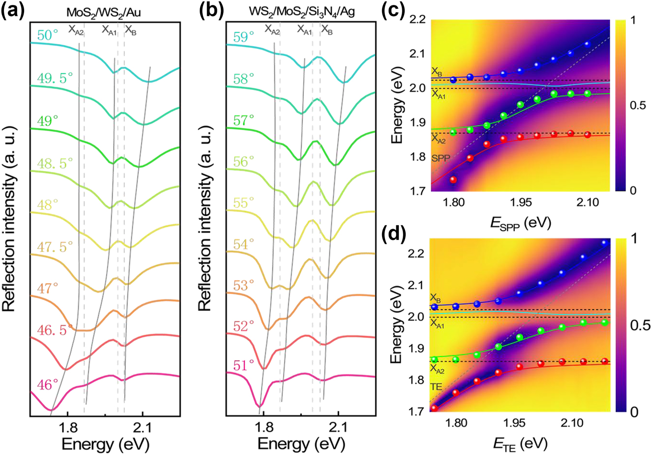
In Figure 4a, we present the scattering spectra of an oligomer of PS nanospheres located on a MoS2/WS2/Au structure, which is excited by using p-polarized light with different incident angles (see also Supplementary Note 9, 10). In all cases, one can identify three scattering peaks (marked by solid lines) in the scattering spectra, corresponding to the hybrid states formed by the coupling between the SPP and the three exciton resonances. The three exciton resonances appear as scattering dips (marked by dashed lines) in the scattering spectrum. At small incident angles, the two dips are relatively shallow and LPB is dominant because the SPP is located on the low-energy side of the exciton resonance. With increasing incident angle, the SPP is gradually shifted to high energies and the scattering spectrum becomes eventually dominated by UPB. In Figure 4c, we plot the two-dimensional scattering spectra measured for the oligomer of PS nanospheres located on the MoS2/WS2/Au structure at different incident angles, corresponding to the SPPs with different energies (E SPP). The dispersion relations of the hybrid states extracted from the scattering spectra (see Figure 4a) are represented by solid symbols while the fitting results based on Hamiltonian are represented by solid curves. It can be seen that the dispersion relations extracted from the scattering spectra (solid symbols) are well fitted by the calculation results (solid curves). In this case, a Rabi splitting energy (ΩSPP) of ∼206.79 meV is observed. In order to find out whether the coupling between the SPP and the three excitons enters the strong coupling regime, we derived the three coupling strengths g SPP-Xi = 69, 52, 35 meV from the fitting results. The dissipation rates of the SPP (γ SPP) and the three exciton resonances (γ i ) are found to be ∼220, ∼33, ∼98, ∼132 meV, respectively. It was found that the strong coupling criterion (g SPP-Xi > (γ SPP + γ Xi )/4) is not satisfied for XA2 and XB due to the large dissipation rates of the SPP and two excitons in MoS2 monolayer [27]. In this case, only the coupling between the SPP and XA1 enters the strong coupling regime owing to the large oscillator strength and small dissipation rate of XA1 in WS2 monolayer. In comparison, the coupling between SPP and two excitons in MoS2 monolayer only reaches intermediate coupling (i.e., g SPP-Xi > (γ SPP − γ Xi )/4). In order to enhance the coupling strength between the SPP and the three excitons, we tried to increase the number of excitons involved in the coupling by using a MoS2/WS2 heterostructure composed of few-layer MoS2 and WS2. In this way, the Rabi splitting energy (ΩSPP) is increased to ∼261.20 meV and the coupling strengths are further enhanced to g SPP-Xi = 88, 57, 50 meV (see Supplementary Note 11). Unfortunately, the strong coupling is still not achieved by using the MoS2/WS2 heterostructure composed of few-layer MoS2 and WS2.

Scattering spectra measured for an oligomer of PS nanospheres placed on a heterobilayer attached on an Au film (a) and a Si3N4/Ag heterostructure (b) at different incident angles. The resonant energies of the three excitons are indicated by the dashed lines. (c, d) Dispersion relations (solid symbols) of the hybrid states extracted from the scattering spectra shown in (a) and (b). Also shown are the fitting results of the dispersion relations based on the Hamiltonian (solid lines). The resonant energies of the surface waves and the three excitons are indicated by dashed lines.
In Figure 4b, we present the scattering spectra of an oligomer of PS nanospheres located on a WS2/MoS2/Si3N4/Ag structure, which is excited by using s-polarized light with different incident angles (see also Supplementary Note 9, 12). Similarly, one can observe three scattering peaks and two scattering dips in all scattering spectra, which originate from the coupling between the TE wave and the three excitons. As compared with the coupling between the SPP and the three excitons, the scattering peaks representing the hybrid states and the scattering dips corresponding to the exciton resonances become more pronounced. In Figure 4d, we plot the two-dimensional scattering spectra measured for the oligomer of PS nanospheres located on the WS2/MoS2/Si3N4/Ag structure at different incident angles, corresponding to the TE waves with different energies (E TE). The dispersion relations of the hybrid states extracted from the scattering spectra (see Figure 4b) are represented by solid symbols while the fitting results are also provided by solid curves. In this case, the Rabi splitting energy is found to be ΩTE ∼237.60 meV and the coupling strengths are derived to be g TE-Xi = 57, 66, 50 meV. The Rabi splitting energy observed for the TE wave is larger than that for the SPP. On the other hand, the dissipation rate of the TE wave (∼64 meV) is much smaller than that of the SPP (∼220 meV). Therefore, the coupling strengths between TE wave and the three exciton resonances satisfy the criterion of strong coupling (i.e., g TE-Xi > (γ TE + γ Xi )/4).
When strong coupling occurs, the hybridization of multiple excitons mediated by the optical mode may result in the efficient energy transfer between them [49]. Apparently, the hybridization of multiple excitons is reflected in the contributions of the excitons in MPB. In Figure S13, we show the current density distribution in a Si3N4/Ag structure calculated for the TE wave at two incident angles. One can see that the current densities are mainly distributed in the Si3N4 layer in both cases. In Figure 5a, we present the current density distribution calculated for a WS2/MoS2/Si3N4/Ag structure at an incident angle of 56°, corresponding to the energy of XA1. Interestingly, it is found that the current density becomes concentrated in the WS2 monolayer, implying the energy transfer from the Si3N4 layer to the WS2 monolayer [50]. Similarly, the current density is concentrated in the MoS2 monolayer when the TE wave is resonant with XA2 at an incident angle of 54°, as shown in Figure 5b. Additionally, the energy transfer is also reflected in the reduced electric field distribution in the Si3N4/Ag structure after the introduction of the WS2/MoS2 heterobilayer (see Supplementary Note 3). Therefore, one can manipulate the energy transfer from the Si3N4 layer to the WS2 or MoS2 monolayer by simply adjusting the incident angle. Based on eq. (2), we also calculated the contributions of the surface wave (SPP or TE wave) and three excitons in each hybrid state, which are reflected in the Hopfield coefficients as a function of the energy of the surface wave, as shown in Figure 5c and d. In both cases, LPBs are mainly composed of the surface wave and XA2. As the energy of the surface wave increases, the fraction of the surface wave decreases while that of XA2 increases. In comparison, UPBs are mainly composed of the surface wave and two excitons (XA1 and XB). With increasing the energy of the surface wave, the fraction of the surface wave increases while that of XB decreases. When the fractions of the surface wave and XB become equal, the fraction of XA1 reaches its maximum, implying the hybridization of XA1 and XB. In MPB1, the fraction of XA2 is quite small (∼3.21 % in Figure 5c and ∼2.67 % in Figure 5d) because its energy is far away from MPB1. In contrast, it can be seen that MBP1 is dominated by XA1 and XB with similar contributions while the contribution of the surface wave is small. In addition, the optical absorption of the excitons usually leads to dips in the scattering spectrum (see Figure 3f). This is the reason why MPB1 cannot be revealed in the reflection or scattering spectrum and only a Rabi splitting energy is observed. In MBP2, XA1 and XA2 have the equal contributions (∼34.07 %) while the fractions of the SPP and XB are ∼28.38 % and ∼3.48 % at E SPP = 1.94 eV, respectively. In comparison, TE wave, XA1, and XA2 have the similar contributions (∼31.89 %, ∼29.48 %, ∼29.48 %) while the fraction of XB is ∼9.28 % at E TE = 1.96 eV. It implies that the TE wave can effectively mediate the hybridization of the three excitons, which suggests the possibility of the energy transfer between the three excitons in MPB.

The hybridization of three excitons in a heterobilayer mediated by the surface waves (a) Current density distribution in a WS2/MoS2 heterobilayer on the Si3N4/Ag heterostructure calculated at the energy of XA1 (2.02 eV) and the incident angle of 56°. (b) Current density distribution in a WS2/MoS2 heterobilayer on the Si3N4/Ag heterostructure calculated at the energy of XA2 (1.88 eV) and the incident angle of 54°. (c, d) Hopfield coefficients derived for the surface wave (SPP or TE wave) and three excitons in UPB, MPB1, MPB2, and LPB as a function of the energy of the surface wave (SPP or TE wave).
3 Conclusions
In summary, we have systematically investigated the coupling between the surface wave (SPP or TE wave) and three excitons (XA1, XA2, XB) in a MoS2/WS2 (or WS2/MoS2) heterobilayer by using two coupling systems (MoS2/WS2/Au and WS2/MoS2/Si3N4/Ag structures). We found that the coupling between the surface wave and three excitons is revealed as anticrossing behaviors in the angle-resolved reflection and scattering spectra. We observed a Rabi splitting energy of ΩSPP ∼206.79 meV for the SPP and an enhanced Rabi splitting energy of ΩTE ∼237.60 meV for the TE wave due to its reduced dissipation rate and enhanced electric field. The similar contributions of the TE wave, XA1, and XA2 in MPB2 indicate clearly the hybridization of the three excitons mediated by the TE wave. The exciton hybridization resulting from the strong coupling between the TE wave and three excitons in a heterobilayer demonstrated in this work suggests the potential applications of energy transfer between the multiple excitons in TMDC heterobilayer in the development of novel photonic devices.
4 Methods
4.1 Sample preparation
In this work, the thicknesses of the Au film, Ag film, and Si3N4 film were designed to be ∼50 nm, ∼50 nm, and ∼100 nm, respectively. The WS2 and MoS2 monolayers used in this work were purchased from SixCarbon Technology Shenzhen. The WS2 and MoS2 monolayers grown by CVD on a SiO2/Si substrate were transferred onto an Au/SiO2 and a Si3N4/Ag/SiO2 substrate by using the following procedure. First, a thin film of poly (methyl methacrylate) (PMMA) was spin-coated onto a WS2 monolayer. Then, the PMMA/WS2 film was separated from the SiO2/Si substrate by etching with KOH (2 mol L−1) at 80 °C. After that, the residual KOH was removed by deionized water, and the PMMA/WS2 film was transferred onto an Au/SiO2. Finally, the PMMA was dissolved by acetone. By using the same method, a MoS2 monolayer was transferred onto the WS2 monolayer, creating a MoS2/WS2 on the Au/SiO2 substrate. Similarly, a WS2/MoS2 heterobilayer was formed on the Si3N4/Ag/SiO2 substrate. The aqueous solution of polystyrene (PS) nanospheres was dropped and dried onto the heterobilayer, forming oligomers of PS nanospheres.
4.2 Optical characterization
In this work, SPP and TE wave can be generated on the surface of an Au film or a Si3N4/Ag heterostructure by using the K–R configuration, as shown in Figure 1a and b. A prism made of SiO2 (K9 glass) was used to couple the p- and s-polarized white light into the optical system through total internal reflection. An inverted microscope (Axio Observer A1, Zeiss), a spectrometer (SR-500i-B1, Andor), and a color charge-coupled device (CCD) (DS-Ri2, Nikon) were used to obtain the scattering spectra and dark-field images of the PS nanospheres.
4.3 Numerical simulations
In this work, the numerical simulations were performed by using the finite-difference time-domain (FDTD) technique. The dielectric constants of Ag and Au were taken from Johnson and Christy [51]. The dielectric constants of MoS2 and WS2 monolayers were obtained from literature [44]. The refractive index of the surrounding media was chosen to be 1.0. In the calculation, the thickness of the MoS2 and WS2 monolayers was chosen to be 1.0 nm. A mesh size as small as 0.5 nm was used to ensure the convergence of numerical simulations and the achievement of accurate results.
Funding source: National Natural Science Foundation of China
Award Identifier / Grant number: 12174123
Award Identifier / Grant number: 12374347
Award Identifier / Grant number: 2022A1515010747
-
Research funding: This work was financially supported by the National Natural Science Foundation of China (Grant Nos. 12174123 and 12374347) and the Guangdong Basic and Applied Basic Research Foundation (Grant No. 2022A1515010747). This work was financially supported by the Scientific Research Innovation Project of Graduate School of South China Normal University.
-
Author contributions: SLa, SLiu, and JY conceived the idea. JY, SLiu, and ZC carried out the sample preparation. JY, SLiu, and SLi carried out optical measurements. JY, SLiu, and WH performed the numerical simulations. SLa, SLi, and JY analyzed the data and wrote the manuscript. SLa supervised the project. All authors have accepted responsibility for the entire content of this manuscript and consented to its submission to the journal, reviewed all the results and approved the final version of the manuscript.
-
Conflict of interest: Authors state no conflict of interest.
-
Data availability: The datasets generated and/or analyzed during the current study are available from the corresponding author upon reasonable request.
References
[1] P. Peng, et al.., “Enhancing coherent light-matter interactions through microcavity-engineered plasmonic resonances,” Phys. Rev. Lett., vol. 119, no. 23, p. 6, 2017, https://doi.org/10.1103/physrevlett.119.233901.Search in Google Scholar
[2] P. Vasa, et al.., “Real-time observation of ultrafast rabi oscillations between excitons and plasmons in metal nanostructures with j-aggregates,” Nat. Photonics, vol. 7, no. 2, pp. 128–132, 2013, https://doi.org/10.1038/nphoton.2012.340.Search in Google Scholar
[3] E. Cao, W. H. Lin, M. T. Sun, W. J. Liang, and Y. Z. Song, “Exciton-plasmon coupling interactions: from principle to applications,” Nanophotonics, vol. 7, no. 1, pp. 145–167, 2018, https://doi.org/10.1515/nanoph-2017-0059.Search in Google Scholar
[4] A. F. Kockum, A. Miranowicz, S. De Liberato, S. Savasta, and F. Nori, “Ultrastrong coupling between light and matter,” Nat. Rev. Phys., vol. 1, no. 1, pp. 19–40, 2019, https://doi.org/10.1038/s42254-018-0006-2.Search in Google Scholar
[5] H. Deng, H. Haug, and Y. Yamamoto, “Exciton-polariton bose-einstein condensation,” Rev. Mod. Phys., vol. 82, no. 2, pp. 1489–1537, 2010, https://doi.org/10.1103/revmodphys.82.1489.Search in Google Scholar
[6] A. Amo, et al.., “Superfluidity of polaritons in semiconductor microcavities,” Nat. Phys., vol. 5, no. 11, pp. 805–810, 2009, https://doi.org/10.1038/nphys1364.Search in Google Scholar
[7] M. D. Fraser, S. Höfling, and Y. Yamamoto, “Physics and applications of exciton-polariton lasers,” Nat. Mater., vol. 15, no. 10, pp. 1049–1052, 2016, https://doi.org/10.1038/nmat4762.Search in Google Scholar PubMed
[8] E. J. Sie, J. McIver, Y. H. Lee, L. Fu, J. Kong, and N. Gedik, “Valley-selective optical Stark effect in monolayer WS2,” Nat. Mater., vol. 14, no. 3, pp. 290–294, 2015, https://doi.org/10.1038/nmat4156.Search in Google Scholar PubMed
[9] A. Ramasubramaniam, “Large excitonic effects in monolayers of molybdenum and tungsten dichalcogenides,” Phys. Rev. B, vol. 86, no. 11, p. 6, 2012, https://doi.org/10.1103/physrevb.86.115409.Search in Google Scholar
[10] B. Munkhbat, et al.., “Electrical control of hybrid monolayer tungsten disulfide-plasmonic nanoantenna light-matter states at cryogenic and room temperatures,” ACS Nano, vol. 14, no. 1, pp. 1196–1206, 2020, https://doi.org/10.1021/acsnano.9b09684.Search in Google Scholar PubMed
[11] Y. Z. Jiang, H. Wang, S. Y. Wen, H. J. Chen, and S. Z. Deng, “Resonance coupling in an individual gold nanorod-monolayer WS2 heterostructure: photoluminescence enhancement with spectral broadening,” ACS Nano, vol. 14, no. 10, pp. 13841–13851, 2020, https://doi.org/10.1021/acsnano.0c06220.Search in Google Scholar PubMed
[12] S. S. Li, et al.., “Routing the exciton emissions of WS2 monolayer with the high-order plasmon modes of Ag nanorods,” Nano Lett., vol. 23, no. 10, pp. 4183–4190, 2023, https://doi.org/10.1021/acs.nanolett.3c00054.Search in Google Scholar PubMed PubMed Central
[13] R. G. Du, H. T. Hu, T. Fu, Z. Shi, S. Zhang, and H. Xu, “How to obtain the correct rabi splitting in a subwavelength interacting system,” Nano Lett., vol. 23, no. 2, pp. 444–450, 2023, https://doi.org/10.1021/acs.nanolett.2c03385.Search in Google Scholar PubMed
[14] S. J. Wang, et al.., “Coherent coupling of WS2 monolayers with metallic photonic nanostructures at room temperature,” Nano Lett., vol. 16, no. 7, pp. 4368–4374, 2016, https://doi.org/10.1021/acs.nanolett.6b01475.Search in Google Scholar PubMed
[15] J. Qin, et al.., “Revealing strong plasmon-exciton coupling between nanogap resonators and two-dimensional semiconductors at ambient conditions,” Phys. Rev. Lett., vol. 124, no. 6, p. 6, 2020, https://doi.org/10.1103/physrevlett.124.063902.Search in Google Scholar
[16] F. Deng, et al.., “Greatly enhanced plasmon-exciton coupling in Si/WS2/Au nanocavities,” Nano Lett., vol. 22, no. 1, pp. 220–228, 2022, https://doi.org/10.1021/acs.nanolett.1c03576.Search in Google Scholar PubMed
[17] H. X. Huang, F. Deng, J. Xiang, S. L. Li, and S. Lan, “Plasmon-exciton coupling in dielectric-metal hybrid nanocavities with an embedded two-dimensional material,” Appl. Surf. Sci., vol. 542, p. 10, 2021, https://doi.org/10.1016/j.apsusc.2020.148660.Search in Google Scholar
[18] S. L. Li, et al.., “Transverse-electric-polarized polaritons propagating in a WS2/Si3N4/Ag heterostructure,” Laser Photon. Rev., vol. 16, no. 12, p. 9, 2022, https://doi.org/10.1002/lpor.202100457.Search in Google Scholar
[19] W. C. He, et al.., “Hybridization of the A- and B-exciton in a WS2 monolayer mediated by the transverse electric polarized wave supported by a Si3N4/Ag heterostructure,” ACS Appl. Nano Mater., vol. 7, no. 16, pp. 19089–19100, 2024. https://doi.org/10.1021/acsanm.4c02981.Search in Google Scholar
[20] V. M. Agranovich, D. M. Basko, G. C. La Rocca, and F. Bassani, “Excitons and optical nonlinearities in hybrid organic-inorganic nanostructures,” J. Phys.-Condes. Matter, vol. 10, no. 42, pp. 9369–9400, 1998, https://doi.org/10.1088/0953-8984/10/42/005.Search in Google Scholar
[21] V. Agranovich, H. Benisty, and C. Weisbuch, “Organic and inorganic quantum wells in a microcavity: frenkel-Wannier-Mott excitons hybridization and energy transformation,” Solid State Commun., vol. 102, no. 8, pp. 631–636, 1997, https://doi.org/10.1016/s0038-1098(96)00433-4.Search in Google Scholar
[22] G. G. Paschos, et al.., “Hybrid organic-inorganic polariton laser,” Sci. Rep., vol. 8, p. 6425, 2017, https://doi.org/10.1038/s41598-018-24599-2.Search in Google Scholar PubMed PubMed Central
[23] M. Sciesiek, et al.., “Long-distance coupling and energy transfer between exciton states in magnetically controlled microcavities,” Commun. Mater., vol. 1, p. 78, 2020, https://doi.org/10.1038/s43246-020-00079-x.Search in Google Scholar
[24] K. Georgiou, R. Jayaprakash, A. Othonos, and D. G. Lidzey, “Ultralong-range polariton-assisted energy transfer in organic microcavities,” Angew. Chem.-Int. Edit., vol. 60, no. 30, pp. 16661–16667, 2021, https://doi.org/10.1002/anie.202105442.Search in Google Scholar PubMed PubMed Central
[25] J. Cuadra, D. G. Baranov, M. Wersäll, R. Verre, T. J. Antosiewicz, and T. Shegai, “Observation of tunable charged exciton polaritons in hybrid monolayer WS2-plasmonic nanoantenna system,” Nano Lett., vol. 18, no. 3, pp. 1777–1785, 2018, https://doi.org/10.1021/acs.nanolett.7b04965.Search in Google Scholar PubMed
[26] A. Rose, J. R. Dunklin, H. Y. Zhang, J. M. Merlo, and J. van de Lagemaat, “Plasmon-mediated coherent superposition of discrete excitons under strong exciton-plasmon coupling in few-layer MoS2 at room temperature,” ACS Photonics, vol. 7, no. 5, pp. 1129–1134, 2020, https://doi.org/10.1021/acsphotonics.0c00233.Search in Google Scholar
[27] K. Wei, Q. R. Liu, Y. X. Tang, Y. Ye, Z. Xu, and T. Jiang, “Charged biexciton polaritons sustaining strong nonlinearity in 2D semiconductor-based nanocavities,” Nat. Commun., vol. 14, no. 1, p. 8, 2023, https://doi.org/10.1038/s41467-023-41079-y.Search in Google Scholar PubMed PubMed Central
[28] D. M. Coles, et al.., “Polariton-mediated energy transfer between organic dyes in a strongly coupled optical microcavity,” Nat. Mater., vol. 13, no. 7, pp. 712–719, 2014, https://doi.org/10.1038/nmat3950.Search in Google Scholar PubMed
[29] K. Georgiou, P. Michetti, L. Z. Gai, M. Cavazzini, Z. Shen, and D. G. Lidzey, “Control over energy transfer between fluorescent BODIPY dyes in a strongly coupled microcavity,” ACS Photonics, vol. 5, no. 1, pp. 258–266, 2018, https://doi.org/10.1021/acsphotonics.7b01002.Search in Google Scholar
[30] W. B. Zhang, et al.., “Steering room-temperature plexcitonic strong coupling: a diexcitonic perspective,” Nano Lett., vol. 21, no. 21, pp. 8979–8986, 2021, https://doi.org/10.1021/acs.nanolett.1c02248.Search in Google Scholar PubMed
[31] B. Miller, et al.., “Long-lived direct and indirect interlayer excitons in van der Waals heterostructures,” Nano Lett., vol. 17, no. 9, pp. 5229–5237, 2017, https://doi.org/10.1021/acs.nanolett.7b01304.Search in Google Scholar PubMed
[32] L. Xie, L. Wang, W. Zhao, S. Liu, W. Huang, and Q. Zhao, “WS2 moire superlattices derived from mechanical flexibility for hydrogen evolution reaction,” Nat. Commun., vol. 12, no. 1, p. 5070, 2021, https://doi.org/10.1038/s41467-021-25381-1.Search in Google Scholar PubMed PubMed Central
[33] L. Zhang, et al.., “Twist-angle dependence of moire excitons in WS2/MoSe2 heterobilayers,” Nat. Commun., vol. 11, no. 1, p. 5888, 2020, https://doi.org/10.1038/s41467-020-19466-6.Search in Google Scholar PubMed PubMed Central
[34] C. Jin, et al.., “Observation of moire excitons in WSe2/WS2 heterostructure superlattices,” Nature, vol. 567, no. 7746, pp. 76–80, 2019, https://doi.org/10.1038/s41586-019-0976-y.Search in Google Scholar PubMed
[35] D. Huang, J. Choi, C. K. Shih, and X. Li, “Excitons in semiconductor moire superlattices,” Nat. Nanotechnol., vol. 17, no. 3, pp. 227–238, 2022, https://doi.org/10.1038/s41565-021-01068-y.Search in Google Scholar PubMed
[36] K. L. Seyler, et al.., “Signatures of moire-trapped valley excitons in MoSe2/WSe2 heterobilayers,” Nature, vol. 567, no. 7746, pp. 66–70, 2019, https://doi.org/10.1038/s41586-019-0957-1.Search in Google Scholar PubMed
[37] T. N. Tran, et al.., “’Enhanced emission from interlayer excitons coupled to plasmonic gap cavities,” Small, vol. 17, no. 45, p. 7, 2021, https://doi.org/10.1002/smll.202103994.Search in Google Scholar PubMed
[38] J. H. Yan, C. R. Ma, Y. C. Huang, and G. W. Yang, “Tunable control of interlayer excitons in WS2/MoS2 heterostructures via strong coupling with enhanced mie resonances,” Adv. Sci., vol. 6, no. 11, p. 9, 2019, https://doi.org/10.1002/advs.201802092.Search in Google Scholar PubMed PubMed Central
[39] G. Zengin, M. Wersäll, S. Nilsson, T. J. Antosiewicz, M. Käll, and T. Shegai, “Realizing strong light-matter interactions between single-nanoparticle plasmons and molecular excitons at ambient conditions,” Phys. Rev. Lett., vol. 114, no. 15, p. 6, 2015, https://doi.org/10.1103/physrevlett.114.157401.Search in Google Scholar PubMed
[40] S. M. Liu, et al.., “Optical introduction and manipulation of plasmon-exciton-trion coupling in a Si/WS2/Au nanocavity,” ACS Nano, vol. 16, pp. 14390–14401, 2022, https://doi.org/10.1021/acsnano.2c04721.Search in Google Scholar PubMed
[41] S. L. Li, L. D. Zhou, M. C. Panmai, J. Xiang, and S. Lan, “Magnetic plasmons induced in a dielectric-metal heterostructure by optical magnetism,” Nanophotonics, vol. 10, no. 10, pp. 2639–2649, 2021, https://doi.org/10.1515/nanoph-2021-0146.Search in Google Scholar
[42] S. Lan, S. Nishikawa, and O. Wada, “Leveraging deep photonic band gaps in photonic crystal impurity bands,” Appl. Phys. Lett., vol. 78, no. 15, pp. 2101–2103, 2001, https://doi.org/10.1063/1.1362328.Search in Google Scholar
[43] T. F. Krauss, “Slow light in photonic crystal waveguides,” J. Phys. D Appl. Phys., vol. 40, no. 9, pp. 2666–2670, 2007, https://doi.org/10.1088/0022-3727/40/9/s07.Search in Google Scholar
[44] Y. Li, et al.., “Measurement of the optical dielectric function of monolayer transition-metal dichalcogenides: MoS2, MoSe2, WS2, and WSe2,” Phys. Rev. B, vol. 90, no. 20, p. 205422, 2014.10.1007/978-3-319-25376-3_5Search in Google Scholar
[45] J. W. Sun, et al.., “Light-emitting plexciton: exploiting plasmon-exciton interaction in the intermediate coupling regime,” ACS Nano, vol. 12, no. 10, pp. 10393–10402, 2018, https://doi.org/10.1021/acsnano.8b05880.Search in Google Scholar PubMed
[46] Y. J. Gong, et al.., “Vertical and in-plane heterostructures from WS2/MoS2 monolayers,” Nat. Mater., vol. 13, no. 12, pp. 1135–1142, 2014, https://doi.org/10.1038/nmat4091.Search in Google Scholar PubMed
[47] X. P. Hong, et al.., “Ultrafast charge transfer in atomically thin MoS2/WS2 heterostructures,” Nat. Nanotechnol., vol. 9, no. 9, pp. 682–686, 2014, https://doi.org/10.1038/nnano.2014.167.Search in Google Scholar PubMed
[48] S. M. Liu, et al.., “Manipulating the exciton dynamics in a MoS2/WS2 heterobilayer with a Si/Au nanocavity,” Laser Photon. Rev., vol. 18, no. 2, p. 11, 2024, https://doi.org/10.1002/lpor.202300850.Search in Google Scholar
[49] K. S. Menghrajani, H. A. Fernandez, G. R. Nash, and W. L. Barnes, “Hybridization of multiple vibrational modes via strong coupling using confined light fields,” Adv. Opt. Mater., vol. 7, no. 18, p. 7, 2019, https://doi.org/10.1002/adom.201900403.Search in Google Scholar
[50] H. Wang, et al.., “Resonance coupling in heterostructures composed of silicon nanosphere and monolayer WS2: a magnetic-dipole-mediated energy transfer process,” ACS Nano, vol. 13, no. 2, pp. 1739–1750, 2019, https://doi.org/10.1021/acsnano.8b07826.Search in Google Scholar PubMed
[51] P. B. Johnson and R. W. Christy, “Optical constants of the noble metals,” Phys. Rev. B, vol. 6, no. 12, pp. 4370–4379, 1972, https://doi.org/10.1103/physrevb.6.4370.Search in Google Scholar
Supplementary Material
This article contains supplementary material (https://doi.org/10.1515/nanoph-2024-0737).
© 2025 the author(s), published by De Gruyter, Berlin/Boston
This work is licensed under the Creative Commons Attribution 4.0 International License.
Articles in the same Issue
- Frontmatter
- Research Articles
- 3D-architected gratings for polarization-sensitive, nature-inspired structural color
- Optical chirality of all dielectric q-BIC metasurface with symmetry breaking
- Waveguide grating couplers with bandwidth beyond 200 nm
- Dual-wavelength multiplexed metasurface holography based on two-photon polymerization lithography
- Centimeter-size achromatic metalens in long-wave infrared
- Exciton hybridization in a WS2/MoS2 heterobilayer mediated by a surface wave via strong photon–exciton coupling
- Wavefront correction with image-based interferometric focus sensing in two-photon microscopy
- Optical transparent metamaterial emitter with multiband compatible camouflage based on femtosecond laser processing
- Exploiting the combined dynamic and geometric phases for optical vortex beam generation using metasurfaces
- Multifunctional metasurface coding for visible vortex beam generation, deflection and focusing