Metalens formed by structured arrays of atomic emitters
-
Francesco Andreoli

 ,
Charlie-Ray Mann
,
Charlie-Ray Mann

Abstract
Arrays of atomic emitters have proven to be a promising platform to manipulate and engineer optical properties, due to their efficient cooperative response to near-resonant light. Here, we theoretically investigate their use as an efficient metalens. We show that, by spatially tailoring the (subwavelength) lattice constants of three consecutive two-dimensional arrays of identical atomic emitters, one can realize a large transmission coefficient with arbitrary position-dependent phase shift, whose robustness against losses is enhanced by the collective response. To characterize the efficiency of this atomic metalens, we perform large-scale numerical simulations involving a substantial number of atoms (N ∼ 5 × 10⁵) that is considerably larger than comparable works. Our results suggest that low-loss, robust optical devices with complex functionalities, ranging from metasurfaces to computer-generated holograms, could be potentially assembled from properly engineered arrays of atomic emitters.
1 Introduction
Light-mediated dipole–dipole interactions in dense ensembles of atom-like emitters, and the wave interference encoded in them, can lead to a cooperative response that is markedly different from that of an isolated emitter [1], [2]. This resource is most effectively harnessed in ordered arrays of emitters with subwavelength lattice constants, where the collective behavior leads to nontrivial phenomena, including an efficient, directional coupling to light. Capitalizing on these properties, many works have explored classical and quantum optical applications of atomic arrays [3], [4], [5], [6], [7], [8], [9], [10], [11], [12], [13], [14], [15], [16], [17], [18], [19], [20], [21], [22], such as the realization of an atomically thin mirror [23], [24], [25]. Perhaps most relevant to the theme of this paper, these arrays have been proposed to implement various classical optical functionalities, including nonreciprocity [26], optical magnetism [27], [28], [29], wavefront engineering [28], [29], [30], polarization control [31], [32], and chiral sensing [33]. Here, we explore a distinct route toward their application as an optical metalens, which only requires the ability to design the positions of identical emitters.
Metalenses have recently emerged as a promising alternative to traditional bulk optics, enabling complex optical operations while retaining subwavelength thicknesses [34], [35]. Their functionality demands simultaneous control over both transmission intensity and phase pattern. In conventional metasurfaces, this is achieved by spatially varying the size, shape, and orientation of individual nanoscatterers, which generally support both electric and magnetic modes. In contrast, the optical response of atom-like quantum emitters is usually dominated by electric dipole transitions, and it offers limited control over their radiative properties. On the other hand, atomic emitters represent an excellent playground to engineer collective effects, as their electronic transition can provide a low-loss, near-resonant optical resonance, with a large scattering cross section
With one eye on integrated photonic devices, here we propose a different mechanism to realize an efficient metalens, which only requires a suitable choice of the positions of solid-state, atom-like emitters. Specifically, we demonstrate that one can achieve full control of the transmission phase in a bi-layer, rectangular array, while maintaining unit transmittance, by simply varying lattice constants and layer spacing. Moreover, by adding a third layer, we show that these transmission properties can be robustly maintained even in the presence of nonradiative losses or other imperfections, owing to the enhanced collective response. Finally, we demonstrate that these structures can be used as building blocks of an efficient metalens, which we verify through large-scale numerical simulations involving a substantial number of emitters (up to N ∼ 5 × 10⁵), which is considerably higher than comparable works [38], [39], [40], [41], [42], [43], [44], [45], [46], [47], [48], [49]. The corresponding code is available for public use at Ref. [50], provided with a broader, user-friendly toolbox to simulate the linear optical response of an arbitrary set of two-level, quantum emitters.
The rest of the paper is structured as follows. First, in Section 2, we review the concept of metalenses, and we introduce the physical system under analysis and its theoretical model. Then, in Section 3, we show how arrays of atomic emitters can be engineered to guarantee unit transmission and tunable phase shift. In Section 4, we use these elements to design an illustrative metalens composed of atomic arrays, and in Section 4.1, we test its behavior through extensive numerics, while optimizing its free parameters via a global particle-swarm algorithm [50]. Finally, in Section 4.2, we probe the resistance of that design against different sources of losses or imperfections.
2 Overview of metalens concept and presentation of our system
Conventional refractive lenses rely on local variations of the optical path inside the lens (where light experiences a higher, positive refractive index) to induce a spatially dependent phase shift. Thereby, the wavefront is shaped in such a way that the output beam focuses at a designed distance, as pictorially represented in Figure 1a. In the past couple of decades, however, the novel idea of developing flat metalenses with much smaller footprints has emerged [51], [52], [53], [54], [55]. These metalenses rely on the electromagnetic response of tailored nanostructures to locally impress abrupt phase shifts on the transmitted light [35], [56], [57], [58], while maintaining a thickness on the order of the wavelength or less [34], [35].
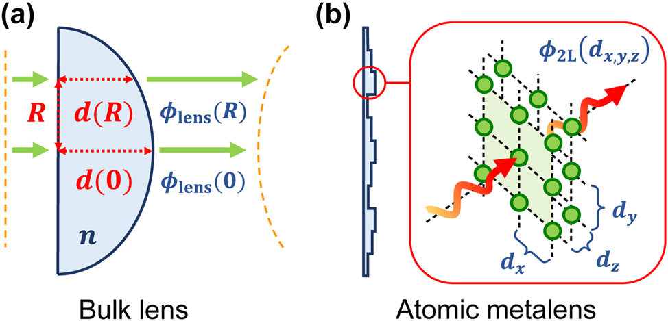
Pictorial comparison between a textbook bulk lens and an atomic metalens. (a) Bulk lens of refractive index n, whose spatially variable optical path d(R) induces a phase delay ϕ lens(R), which curves the incident wavefront, to make it focus at the target distance. (b) Schematic structure of an atomic metalens. Its building blocks consist of at least two atomic arrays in series, whose subwavelength lattice constants d x,y,z < λ 0 can be engineered to ideally ensure a fully directional transmission, with an arbitrary phase shift. For a realistic, lossy system, three atomic layers are required to enhance the robustness to losses.
Regardless of physical implementation, the function of a simple ideal lens of focal length f on a monochromatic input beam of light with wavevector
upon transmission. This phase is defined modulo 2π, and here we adopt the convention −π ≤ ϕ
lens ≤ π. Moreover, we define the transverse coordinate
Although the theory that we present will be rather general, from an experimental perspective color centers in diamond can offer a promising framework for its implementation, as they stand out for their excellent optical properties [60]. Specifically, they behave as atom-like emitters with well-defined selection rules and a dipolar response aligned along one of the four possible tetrahedral directions of the diamond lattice [60], [61], [62], [63], [64], [65]. Current fabrication technologies, moreover, offer good control over their spatial position [66], up to
More specifically, we focus on the case of Silicon Vacancy (SiV) centers, which we model as idealized two-level emitters with resonant frequency 2πc/ω
0 ≈ 737 nm. In this model, we assume that the fabrication process permits to preferentially discriminate over the four possible orientations, so that all the emitters have the same dipole matrix element
3 Global control of transmission
We now introduce the theoretical framework to capture the linear optical response of a collection of N quantum emitters in response to a monochromatic classical field, allowing for arbitrary positions. For intensities below the saturation threshold, the nonlinear behavior of a quantum emitter is negligible, and each SiV linearly responds to near-resonant light with a characteristic polarizability
The total field at any point in space consists of the sum between the incident field E in(r) and the field rescattered by the atomic emitters, reading
where the dyadic Green’s tensor
defines the scattering pattern of each atomic dipole
The dipole moments of the emitters are linearly driven by the total field at their position, leading to the self-consistent coupled-dipole equations [81]
which account for the process of multiple light scattering in a nonperturbative fashion. Here, we defined the parameter
3.1 Transmission of M arrays in series
Our goal is to show how the transverse lattice constants d
x,y
and distances d
z
of a stack of M ≥ 2, 2D rectangular arrays of atomic emitters can be chosen to impress an arbitrary phase shift, while preserving unit transmission. To do so, it is useful to define the atomic dipoles as p
mj
, whose double indices identify the positions as
We first review the cooperative behavior of a single, rectangular 2D array, placed at z = z
m
. For simplicity, we assume that the input light is a
Once excited, the field coherently scattered by each array can be calculated via Eq. (2). Due to the discrete translational symmetry, the array can add a reciprocal lattice vector
where Ω0 = Ωin(0, 0), while the terms
1D, cooperative model for a 3D atomic array, illuminated at normal incidence. We consider a stack of M subwavelength, rectangular 2D arrays of atomic emitters with constant d
x,y
, separated by a longitudinal distance d
z
. The emitters are identical two-level systems, with a resonant frequency ω
0 and spontaneous emission rate Γ0, which identify the polarizability α
0(Δ = ω − ω
0, Γ0). The layers are illuminated at normal incidence and can scatter light only in this direction (red, wavy arrows), since the other diffraction orders are evanescent (blue, shaded, wavy arrows). Within each 2D array, the optical response is characterized by a single-mode, collective transition, with cooperative resonant frequency ω
coop and decay rate
After solving the set of collective coupled-dipole equations Eq. (5), one can use Eq. (2) to reconstruct the field. Since each array can only selectively radiate into the same mode of the input light, it is straightforward to define the far-field transmission and reflection coefficients [16]
We notice that these equations can be solved without fixing any value of Ω0, due to the linearity of the optical response p
m
∝ Ω0. Similarly, Eq. (5) can be directly solved for the dimensionless ratios
To conclude, for the following calculations, we find it favorable to restrict to a regime where the evanescent fields
3.2 Phase control
A metalens is typically composed of nanostructures as wide as ≲λ 0, which transmit the majority of light and impress a tunable phase shift. We now show how the lattice constants of a stack of atomic arrays can be similarly engineered, aiming to use them as the building blocks of an atomic metalens. Hereafter, we define the phase of transmission as ϕ ML = arg t ML ∈ (−π, π], and we explicitly focus on the resonant case Δ = 0, although the same method can be extended to near-resonant light.
We begin by considering the simplest scenario, corresponding to a single atomic layer in the lossless regime of Γ′ = 0. The complex value of t
1L depends on the difference between the collective resonance frequency ω
coop(d
x,y
) and the frequency of the incoming light, which we fixed to the resonance frequency of a single emitter (i.e., Δ = 0). In principle, this means that the transmission phase ϕ
1L = arg t
1L is itself tunable via the choice of lattice constants d
x,y
. Nonetheless, using Eqs. (5) and (6), it is easy to show that high transmission and arbitrary phase cannot be achieved with one layer of atoms, as the conditions of reciprocity
For an ideal system, we can achieve perfect transmission with arbitrary phase by considering a bi-layer (M = 2) array. As long as
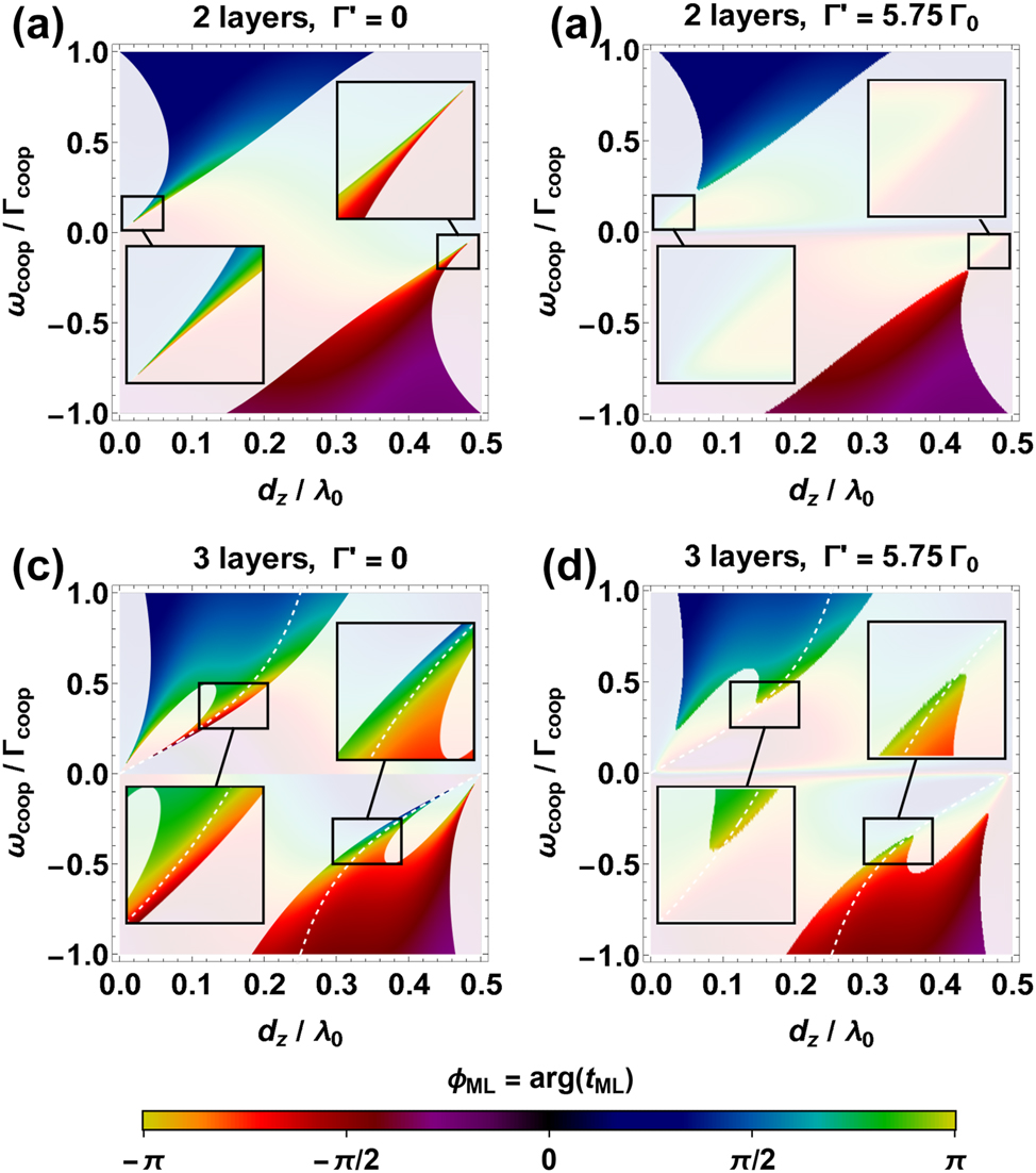
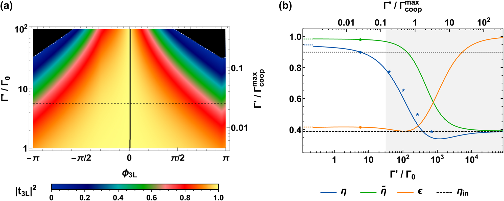
Transmission of a multilayer atomic array, as a function of ω coop(d x,y )/Γcoop(d x,y ) and d z . (a, b) Colorbar representation of the phase shift ϕ 2L = arg t 2L of two atomic layers, given either Γ′ = 0 (a) or Γ′ = 5.75Γ0 (b). The transverse lattice constants are varied within the range λ 0 > d x,y ≥ d min = 0.03λ 0, which means that Γ′/Γcoop(d x,y ) ≳ 0.03. When different choices of d x and d y are associated to the same value of ω coop(d x,y )/Γcoop(d x,y ), the pair with the highest cooperative decay is selected. The region where |t 2L|2 < 0.5 is represented by a white shaded area, while the insets show the relevant case of ϕ 2L ≡ arg t 2L ∼ ±π and |t 2L|2 ≥ 0.5. (c, d) Same structure of subfigures (a) and (b), but for the three-layer case. The white dashed lines represent the chosen branch d z (d x,y ) that maximizes the transmittance. Along this path, the insets show that both the phase ϕ 3L = ±π and the transmission |t 3L|2 ≥ 0.5 can be simultaneously obtained over a much broader bandwidth (c), becoming more resistant to the losses (d).
However, the phase range contracts as
In general, M − 1 transparency conditions d
z
(d
x,y
) similar to that of a Fabry–Perot cavity can be found for arbitrary values of M [89], and the addition of more atomic layers M > 2 is important to restore the resistance to losses around |ϕ
ML| ∼ π. This can be intuitively understood for even number of layers M, as a proper choice of d
z
(d
x,y
) can make the system act as M/2 cascaded cavities, so that
To define the proper relations d z (d x,y ) between the longitudinal and transverse lattice constants, we introduce a closed-form solution of Eq. (6), which reads [90]
where the function u M (k, d z ) = sin(Mkd z )/sin(kd z ) relates the finite-size behavior to the dispersion relation k(d x,y,z ) = k(ω coop(d x,y )/Γcoop(d x,y ), d z ) of an infinite chain [16]. In the lossless regime of Γ′ = 0, the unit transmission t ML = (−1) a exp(iMk 0 d z ) is ensured by fixing d z (d x,y ) to fulfill k(d x,y,z ) = aπ/(Md z ), where the natural number a = 1, …, M − 1 identifies the M − 1 possible solutions within the first Brillouin zone. With this choice, the field acquires a total phase shift of ϕ ML(d x,y ) = Mk 0 d z (d x,y ) + aπ with respect to propagation in the bulk environment.
In our M = 3 case, we choose the branch of d
z
(d
x,y
) with a = 2, as represented in Figure 3c and 3d by a dashed, white line. When spanning d
x,y
, this is associated to high transmittance and complete phase control, in both the lossless (Figure 3c) and lossy Γ′ = 5.75Γ0 (Figure 3d) regimes. More specifically, we scan the transverse lattice constants d
x,y
along the two straight lines (d
x
= d
min) ∪ (d
min ≤ d
y
< λ
0) and (d
min ≤ d
x
< λ
0) ∪ (d
y
= d
min), which allows to associate a unique set of spacings d
x,y,z
to any value of ϕ
3L(d
x,y
) = arg t
3L(d
x,y
, d
z
(d
x,y
)). This correspondence is represented in Figure 4a, showing that only a limited set of distances λ
0/6 ≤ d
z
≤ λ
0/3 is required, thus implying a maximum thickness of
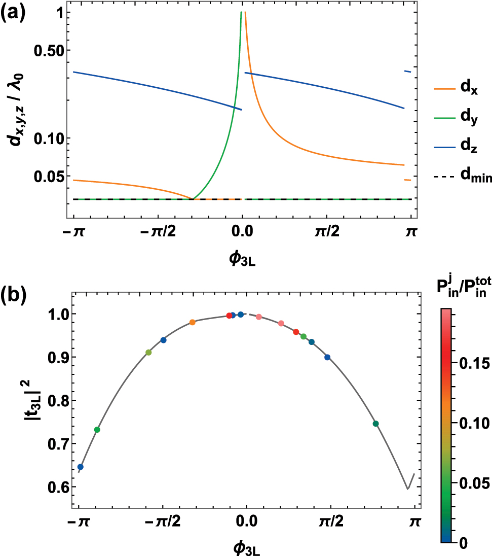
Lattice constants d
x,y,z
and transmittance |t
3L|2 as a function of phase ϕ
3L, given Γ′ = 5.75Γ0. (a) We scan the transverse lattice constants along the two straight lines (d
x
= d
min) ∪ (d
min ≤ d
y
< λ
0) and (d
min ≤ d
x
< λ
0) ∪ (d
y
= d
min), with d
min = 0.03λ
0 (black, dashed line). At the same time, the choice of d
z
(d
x,y
) that maximizes the transmittance allows to associate a unique set of lattice constants (colored lines) to any phase ϕ
3L = arg t
3L(d
x,y
, d
z
(d
x,y
)) (horizontal axis). (b) Transmittance |t
3L|2 as a function of the phase ϕ
3L (gray line). The colored points are associated to the rings composing the illustrative atomic metalens discussed in Section 4. Their colors are associated to the relative power of the input light over their area, i.e.,
We notice that those phases within the interval of 0 ≲ ϕ 3L ≲ 0.01π cannot be engineered, due to the limited value of max ω coop ≈ 28Γcoop for d min ≤ d x,y ≤ λ 0. Nonetheless, for practical applications such as a metalens, this range can be approximated with exactly ϕ 3L = 0 (i.e., no emitters), as its span is negligible compared to typical discretization scales.
4 Atomic metalens
To design an atomic metalens out of three-layer atomic arrays, one needs to spatially tune the lattice constants d
x,y
, to make the phase shift ϕ
3L(d
x,y
) match that of an ideal lens, i.e., the value ϕ
lens(R) specified in Eq. (1). To define a concrete recipe, we divide the transverse plane into concentric rings j = 1, 2… of radius R
j
= jΔR (see Figure 5a), and we associate to each ring the central phase shift ϕ
j
≡ ϕ
lens(R
j−1/2 + R
j
/2), by using Eq. (1). Here, we recall that the initial phase ϕ
0 is a free parameter. At this point, we impose
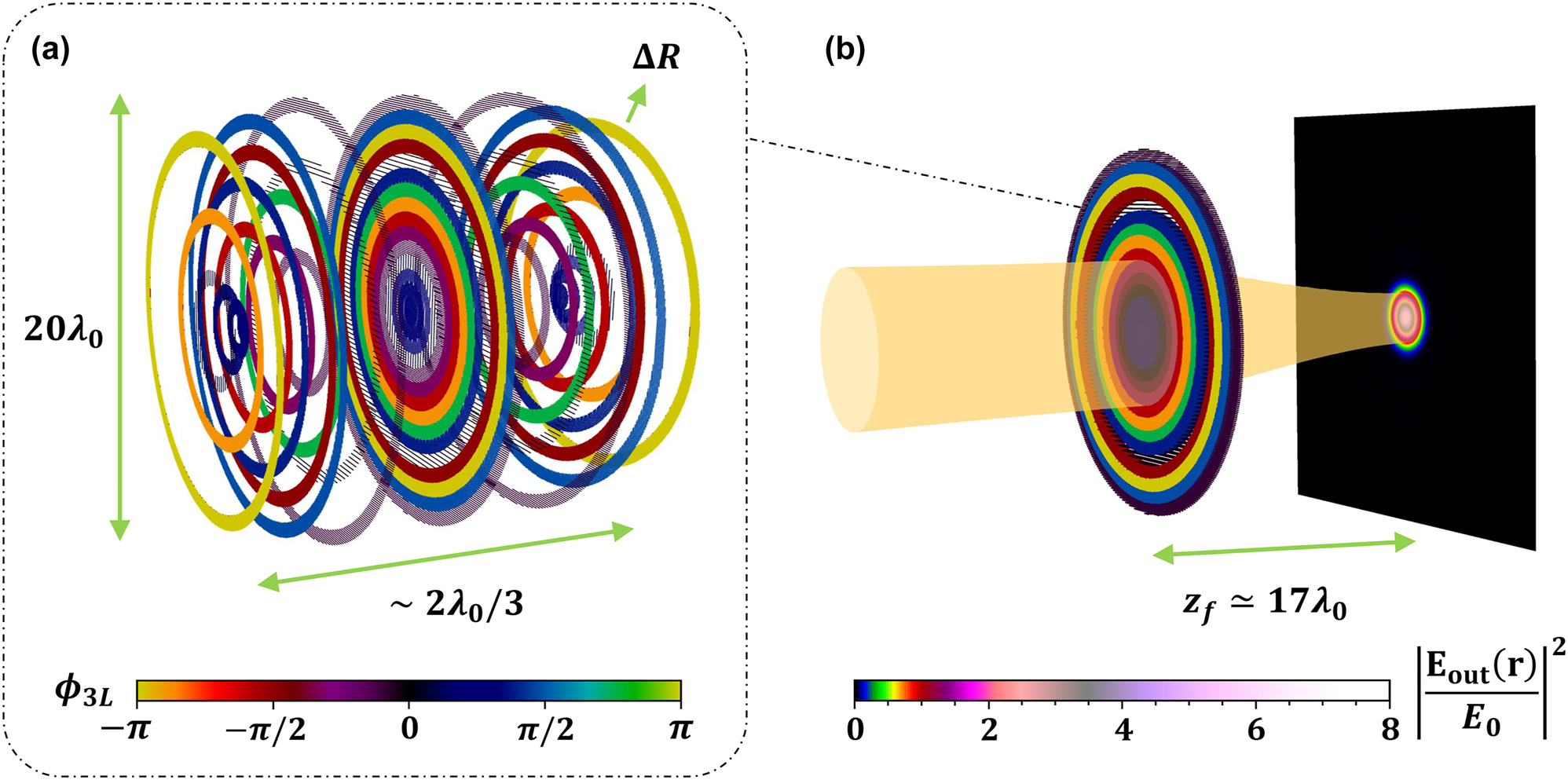
Structure of an atomic metalens, with focal length f = 20λ
0 and radius R
lens = 10λ
0. (a) 3D representation of the atomic metalens, where each point depicts the position of one atom. This atomic metalens is composed of 15 concentric rings of thickness ΔR ≈ 2λ
0/3, with a buffer-zone parameter α ≈ 0.2. The lens has a width of Δz ≈ 2λ
0/3, much thinner than the total diameter of 20λ
0. The atoms belonging to the j-th ring have the same lattice constants
At the interface between the finite rings, the abrupt change of lattice constants can potentially scatter light into unwanted diffraction modes. To soften these detrimental effects, in the
To conclude, we remark that for each target focal length f, our atomic metalens is defined up to three free parameters, which are an overall phase shift −π < ϕ 0 ≤ π, the ring thickness d min ≪ ΔR ≲ λ 0, and the buffer fraction 0 ≤ α ≤ 1/2.
4.1 Numerical simulations
To check our design, we want to estimate the efficiency of an atomic metalens with focal length f and centered around z = 0. To this aim, we fix the atomic positions, and we illuminate the system at normal incidence with a
To characterize the metalens performance, we quantify the fraction η = P
η
/P
in of power P
η
that is correctly transmitted into the target, ideal Gaussian mode E
f
, divided by the total input power P
in [91]. Operatively, this efficiency can be obtained by analytically projecting E
out into the target mode E
f
, namely η = |⟨E
f
|E
out⟩|2. This projection has a simple, closed-form expression, which is detailed in Appendix D. Another quantity of interest is the overlap between the transmitted field and the input field ϵ = |⟨E
in|E
out⟩|2. Obviously, one would aim to operate in a regime where η ∼ 1, while ϵ ≪ 1, with the latter inequality signifying that the lens performs some non-negligible transformation. Finally, we notice that, for certain applications, the main requirement is the identification of the focal spot over the background of transmitted light. In view of that, we define the signal-to-background ratio
To show the potential of our scheme, we can now discuss an illustrative full-scale simulation of a metalens with focal length f = 20λ
0 and radius R
lens = 10λ
0, illuminated by an input Gaussian beam of waist w
0 = 4λ
0. In this illustrative scenario, the ideal magnification would read
The numerical results are shown in Figure 6, where we plot the relative intensity of the total field |E out(R, z)/E 0|2, calculated on the horizontal plane y = 0 (top row) and at the expected focal plane z = z f ≃ 17λ 0 (bottom row). The column on the left (Figure 6a and 6d) shows the ideal values that one would expect for a textbook, ideal lens, i.e., E f (R, z). This is compared to the numerical simulations of the atomic metalens, calculated for the lossy case Γ′ = 5.75Γ0 (right column, Figure 6b and 6e). Very similar plots are obtained when studying the lossless case Γ′ = 0, or when plotting the intensity on the plane x = 0.
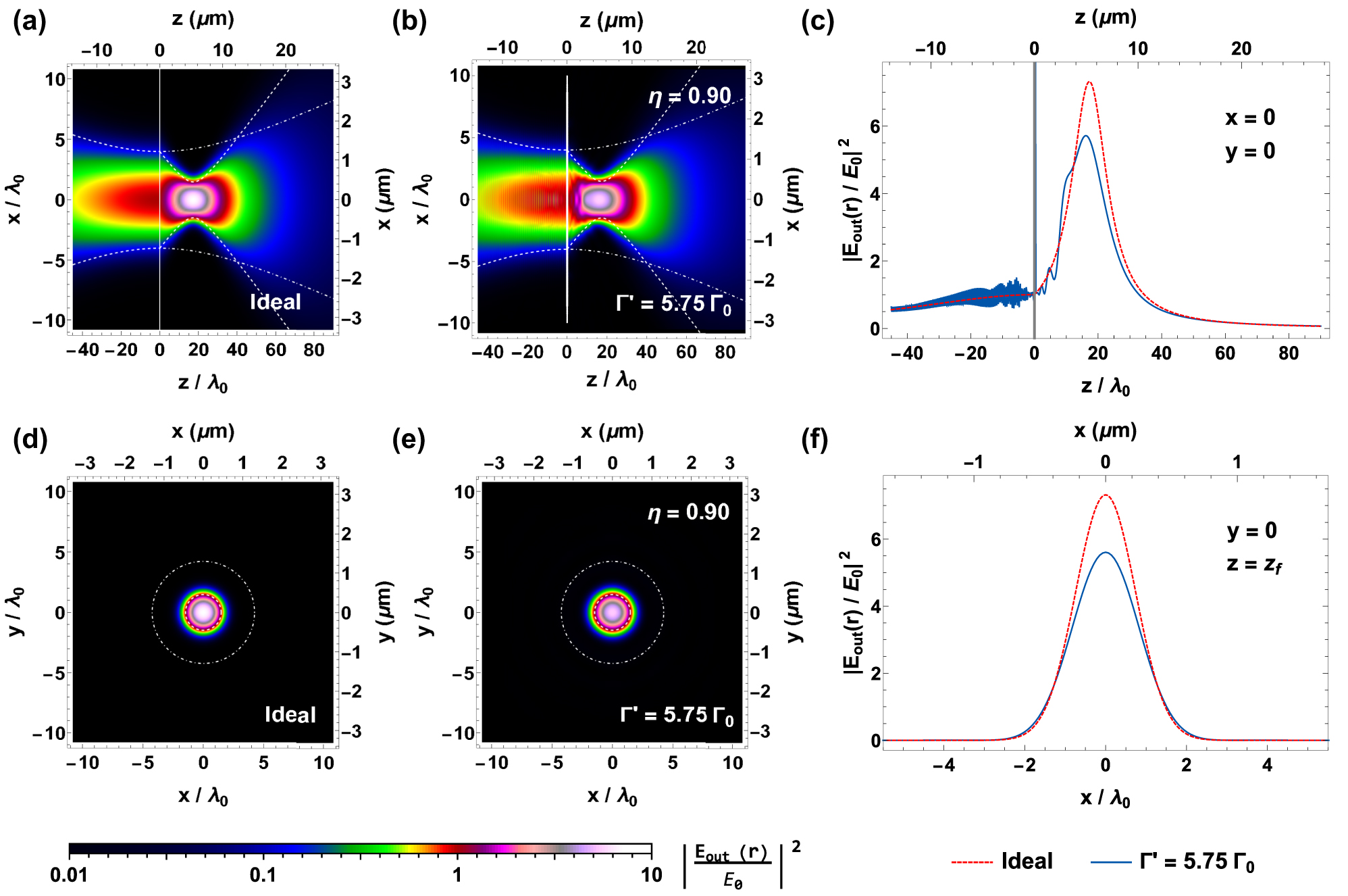
Illustrative case of an atomic metalens with focal length f = 20λ
0, radius R
lens = 10λ
0, and parameters ΔR ≈ 2λ
0/3, ϕ
0 ≈ −2.06, and α ≈ 0.2, illuminated by a resonant Gaussian beam with waist w
0 = 4λ
0. The figures show the relative intensity of the total field |E
out(R, z)/E
0|2, calculated on the planes y = 0 (top row, subfigures a, b) and z = z
f
≃ 17λ
0 (bottom row, subfigures d, e). The subplots (a, d) represent the ideal case of a textbook lens, while the subplots (b, e) show the results of the numerical simulations with Γ′ = 5.75Γ0. The dashed, white lines represent the ideal value of the beam waist w(z), while the dot-dashed, white lines show the waist of the input beam if no lens were present. The efficiency of the lossy Γ′ = 5.75Γ0 case, estimated from the simulations, reads η ≃ 0.90, while the signal-to-background ratio reads
We benchmark the optical response of the atomic metalens from our simulations, finding an efficiency η ≃ 0.95 and an intensity enhancement at the focal point of |E
out(0, z
f
)/E
0|2 ≃ 6.03, in the lossless regime of Γ′ = 0. Similarly, in the lossy case of Γ′ = 5.75Γ0, we obtain the values η ≃ 0.90 and |E
out(0, z
f
)/E
0|2 ≃ 5.60. This value can be appreciated in Figure 6c and 6f, where we compare the ideal (red, dashed line) and numerical (blue, solid line) field intensity along, respectively, either the z axis (in the x = y = 0 plane) or the x axis (at the focal plane). These high efficiencies stand out when considering the much lower overlap ϵ ≃ 0.42 between the output field and the input beam, which means that the atomic metalens is nontrivially acting on the input beam. Finally, both the lossy and the lossless cases exhibit a high signal-to-background ratio, reading
Although the atomic metalens was designed to operate for resonant light at Δ = 0, a similar reasoning allows to qualitatively predict the spectral bandwidth where the efficiency remains high. To show this, we calculate the cooperative decay rates
To conclude, it is interesting to investigate how the response is modified when increasing the focusing ability of the lens, as quantified by the magnification
![Figure 7:
Efficiency of an atomic metalens as a function of the magnification, given Γ′ = 5.75Γ0. We fix both the waist of the input beam to w
0 = 4λ
0, and the radius of the lens R
lens = 10λ
0, while showing the efficiency η (blue points), signal-to-background ratio
η
̃
$\tilde {\eta }$
(green points), and input-field overlap ϵ (orange points) as a function of the magnification
1
≤
M
≲
w
0
/
λ
0
=
4
$1\le \mathcal{M}< sim {w}_{0}/{\lambda }_{0}=4$
. For each point, we perform a particle-swarm optimization of the free parameters ϕ
0, α, and ΔR to maximize the efficiency η [50]. By fitting the data, we infer the empirical scalings
η
≈
1.06
−
0.06
M
$\eta \approx 1.06-0.06\mathcal{M}$
,
η
̃
≈
1.05
−
0.03
M
$\tilde {\eta }\approx 1.05-0.03\mathcal{M}$
and
ϵ
≈
−
0.04
+
1.23
/
M
${\epsilon}\approx -0.04+1.23/\mathcal{M}$
(colored, dashed lines). The black, dotted line shows the reference value of 0.8.](/document/doi/10.1515/nanoph-2024-0603/asset/graphic/j_nanoph-2024-0603_fig_007.jpg)
Efficiency of an atomic metalens as a function of the magnification, given Γ′ = 5.75Γ0. We fix both the waist of the input beam to w
0 = 4λ
0, and the radius of the lens R
lens = 10λ
0, while showing the efficiency η (blue points), signal-to-background ratio
4.2 Losses and imperfections
Up to now, the presence of experimental losses and imperfections has been modeled by the addition of a detrimental broadening Γ′ ≈ 5.75Γ0, whose value was chosen to qualitatively capture some key properties of state-of-the-art experiments with color centers in diamond. While our studies up to now represent an optimistic scenario, here we investigate the performance of the metalens as the broadening rate Γ′ increases, or when the atoms are subject to increasing spatial disorder.
First, we study the resistance to increasing levels of broadening Γ′, which we compare with the maximum cooperative decay rate
Resistance to nonradiative losses. (a) Transmission of a three-layer array, given increasing levels of Γ′. Similarly to Figure 4b, we use our definition of d
x,y,y
to associate a unique transmittance |t
3L|2 (color scheme) to any target phase ϕ
3L (horizontal axis). We then vary Γ′ (vertical axis) to track the change in the transmittance. We notice that an almost identical plot is obtained when numerically optimizing the choices of d
x,y,z
≥ d
min = 0.03λ
0 to maximize transmittance, proving the validity of our scheme. The black, dashed line highlights the particular case Γ′ = 5.75Γ0. The black areas (bounded by dotted, white lines) identify regions of the parameter space that cannot be obtained with any choice of d
x,y,z
. (b) Efficiency as a function of Γ′, given an atomic metalens with focal length f = 20λ
0, radius R
lens = 10λ
0, and construction parameters ΔR ≈ 2λ
0/3, ϕ
0 ≈ −2.06, and α ≈ 0.2, illuminated by a Gaussian beam with w
0 = 4λ
0. The lines show the efficiency η (blue), signal-to-background ratio
To get further insights, it is instructive to explicitly focus on the illustrative atomic metalens of Figure 6, with focal length f = 20λ
0, radius R
lens = 10λ
0, and parameters ΔR ≈ 2λ
0/3, ϕ
0 ≃ −2.06, and α ≈ 0.2. In Figure 8b, we discuss the overall response of this metalens, for broadening levels up to
Finally, we discuss the effect of disorder in the atomic positions, defined by randomly displacing each atomic emitter inside a 3D sphere of radius δd, with a uniform distribution. In Figure 9, we represent with colored points the same quantities of Figure 8b, as a function of increasing disorder δd. As intuitively expected, when the displacement is comparable to d
min, then the efficiency is strongly undermined, with η ∼ 0. In that regime, the transmitted light is so randomly altered, that it does not overlap anymore with the input field either, and one gets ϵ ∼ 0. Nonetheless, we notice that the signal-to-background ratio exhibits more robust properties, with
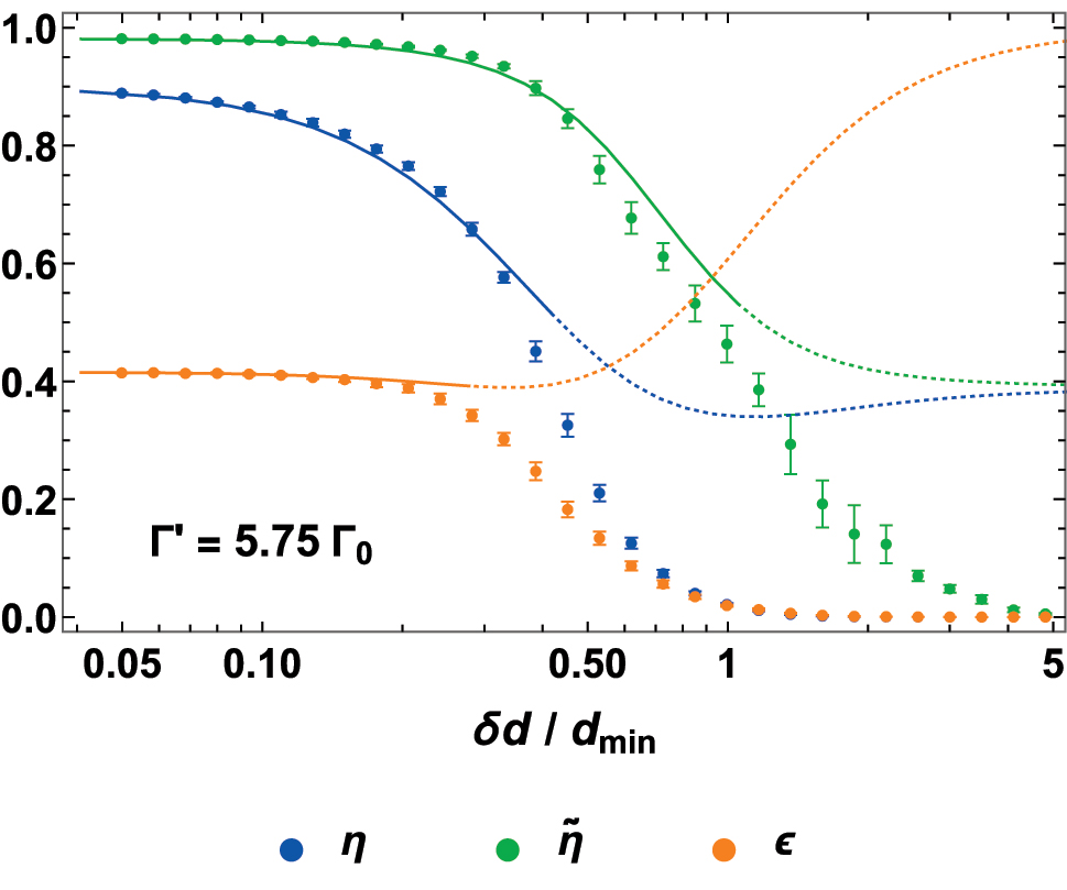
Resistance to additional position disorder. The data are calculated for the atomic metalens with focal length f = 20λ
0, radius R
lens ≃ 9λ
0, and construction parameters ΔR ≈ 2λ
0/3, ϕ
0 ≈ −2.06, and α ≈ 0.2, illuminated by a Gaussian beam with w
0 = 4λ
0. The horizontal axis represents the random displacement radius δd in units of the minimum lattice constant d
min. The points represent the average efficiency (η, blue), signal-to-background ratio (
As detailed in Appendix A.2, small displacements in a 2D array (or in a stack of arrays) can be well described by a supplementary broadening
5 Discussion
Complete wavefront shaping requires the simultaneous achievement of high transmittance and full phase control. Usually, metamaterials achieve these requirements by engineering the local properties of the individual scatterers, such as, for example, the shape of nanoresonators. Solid-state, atom-like emitters, however, do not provide the same manufacturing flexibility, and theoretical proposals of atom-based metasurfaces rely on external drives with subwavelength intensity profiles to locally change the emitter properties [28], [29], [30], [37]. Still, the possibility of engineering a complex optical response by solely implanting atomic-scale scatterers in a solid-state environment represents an interesting perspective on device integration and miniaturizability [95], especially when considering the thick substrate that is usually required by standard metasurfaces (typically
In this work, we showed that stacks of two or more consecutive arrays of solid-state emitters can be engineered to fulfill the necessary requirements of transmittance and phase control, by only choosing proper lattice constants that ensure their correct collective response. Via large-scale numerical simulations [50], we argued that these elements can be combined as the building blocks of a metalens, whose efficiency is robust to losses and other imperfections, due to the collective enhancement of the optical response. This is achieved within a maximum thickness of
The core design of our atomic metalens is based on an analytic map between any discretized phase pattern and the corresponding set of lattice constants. Although this scheme is intrinsically scalable, the design is complete only up to three macroscopic free variables, given by the overall phase shift ϕ 0 of the metalens, the discretization size of the rings ΔR, and the fraction α of “buffer zones”. The scalability of this optimization step is not trivial, as it involves large-scale coupled-dipole simulations. To facilitate it, one possible strategy would consist of investigating whether each ring made of discrete atoms could be modeled by smooth, flat mirrors, with proper transmission and reflection coefficients. This would enable simulation via optical commercial software, with a computational complexity decoupled from the number of dipoles [97], [98], [99], [100], [101]. Alternatively, it would be interesting to explore if a target, collective optical response could be obtained with far fewer emitters, by inverse-designing their positions through proper optimization algorithms [102]. Some preliminary numerical simulations suggest that adjoint methods might be a promising path in this direction [103].
With our scheme, the total efficiency is protected by the collective response, even if the losses of the individual scatterers are non-negligible Γ′ ≫ Γ0. Similar considerations apply beyond the case of atom-like emitters, to any set of optical scatterers with a well-defined resonant, dipolar response, and a ratio between scattering and total cross section equating
Finally, it is interesting to mention some specific features of color centers in diamond, whose two-level nature provides nontrivial properties both at the classical and at the quantum level. For example, an atomic metalens based on SiVs would be extremely narrowband and polarization sensitive, finding possible applications in terms of spectral filtering [106], [107], [108], tunability [109], or polarization control [110], [111]. Furthermore, color centers are highly saturable objects, due to their intrinsic nonlinearity, and this behavior would automatically limit the metalens response up to a threshold intensity of light.
At the quantum level, it is known that color centers can be embedded inside a metasurface to enhance some of their functionalities, for example as single-photon sources [112]. It would be interesting to explore if enhanced, collective properties of an ensemble of color centers could be more easily designed by engineering the emitters to act as a nonlocal metasurface. Some evidence exist, for example, that stacks of two atomic arrays can exhibit enhanced nonlinear correlations [86]. More generally, a metasurface based on color centers could provide a possible playground for the emerging contexts of quantum metasurfaces [113] and quantum holography [114], [115].
Methods: We numerically simulate the optical response of the system by solving the coupled-dipole equations of Eqs. (2) and (4), whose computational time scales as ∼N
3, where N is the number of atomic dipoles. The input Gaussian beam must have a waist w
0 much smaller than the radius R
lens of the atomic metalens, to avoid scattering from the edges or a non-negligible fraction of light passing outside the lens. Due to the paraxial approximation, however, this imposes the constraint λ
0 ≪ w
0 ≪ R
lens. Furthermore, to counteract the effects of the broadening Γ′, one must work with small lattice constants down to d
min ≈ 0.03λ0, thus explaining the necessity of simulating up to N ∼ 5 × 10⁵ atomic dipoles. To accomplish this task, we exploit the fact that the system is symmetric for
Funding source: HORIZON EUROPE Marie Sklodowska-Curie Actions
Award Identifier / Grant number: 101068503
Funding source: Generalitat de Catalunya
Award Identifier / Grant number: 2021 SGR 01442
Award Identifier / Grant number: CERCA
Funding source: Horizon 2020 Framework Programme
Award Identifier / Grant number: 101017733
Funding source: European Research Council
Award Identifier / Grant number: 101002107
Funding source: Government of Spain
Award Identifier / Grant number: CEX2019- 000910-S
Award Identifier / Grant number: NextGenerationEU/PRTR PCI2022-132945
Funding source: HORIZON EUROPE European Innovation Council
Award Identifier / Grant number: 101115420
Award Identifier / Grant number: 899275
Funding source: H2020 Marie Skłodowska-Curie Actions
Award Identifier / Grant number: 713729
-
Research funding: ICFOstepstone – PhD Programme funded by the European Union’s Horizon 2020 research and innovation programme under the Marie Sklodowska-Curie grant agreement No. 713729. Marie Sklodowska-Curie Actions Postdoctoral Fellowship ATOMAG (grant agreement No. 101068503). European Research Council grant agreement No. 101002107 (NEWSPIN), FET-Open grant agreement No 899275 (DAALI), EIC Pathfinder Grant No. 101115420 (PANDA). Severo Ochoa Grant CEX2019-000910-S [MCIN/AEI/10.13039/501100011033]. QuantERA II project QuSiED, co-funded by the European Union Horizon 2020 research and innovation programme (No. 101017733) and the Government of Spain (European Union NextGenerationEU/PRTR PCI2022-132945 funded by MCIN/AEI/10.13039/501100011033). Generalitat de Catalunya (CERCA program and AGAUR Project No. 2021 SGR 01442), Fundacio Cellex, and Fundacio Mir-Puig.
-
Author contributions: All authors have accepted responsibility for the entire content of this manuscript and approved its submission.
-
Conflict of interest: Authors state no conflicts of interest.
-
Data availability: No experimental datasets were generated or analyzed during the current study. All codes used to perform the numerical simulations are available upon request.
Appendix A: Coherent scattering by silicon vacancy centers
In this appendix, we explain more in detail our model of SiV centers in diamond as two-level, dipole emitters. We stress that similar considerations apply to other group IV color centers [60]. The Zero-Phonon-Line (ZPL) of a SiV is centered around 2πc/ω
0 ≈ 737 nm and is composed of four resonances, associated to the spin–orbit splitting into two ground
In view of all these considerations, we model the system by considering that the lifetime τ of the excited state
For each emitter, the quantity
A.1 Inhomogeneous broadening
To model the presence of inhomogeneous broadening, we assume that each atom of the array has a shifted resonance frequency
where we defined
In Figure A.1, we numerically check the soundness of this assumption by evaluating the spectrum of transmission |t(Δ)|2 of a 2D square array of size L = 6.4λ
0 and lattice constant d
x,y
= 0.2λ
0, illuminated by a Gaussian beam of waist w
0 = L/4. Here, t(Δ) is calculated by projecting the output field of Eq. (2) onto the same mode as the input beam [80], as also detailed in Appendix D. We compare the analytic model of Γ′ = Γinhom = 5Γ0 (red line), with the numerical results obtained by considering a Lorentzian distribution of resonant frequencies with σ
Lorentz = 2.5Γ0 (blue points), observing a remarkable agreement. As a reference, the green points show the case of resonances
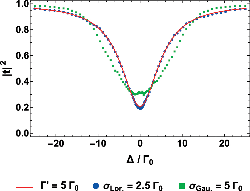
Effects of inhomogeneous broadening on a 2D atomic array. Transmission spectrum of a finite 2D square lattice with transverse size L = 6.4λ
0 and lattice constants d
x,y
= 0.2λ
0, illuminated by a Gaussian beam of waist w
0 = L/4. The blue points (green squares) are calculated by solving the inhomogeneous version of the coupled-dipole equations Eq. (4) with randomly shifted polarizabilities
Rather than an exact model of a specific set of experimental data, we aim to capture a reasonable, qualitative description of the effects of inhomogeneous broadening. To this aim, we consider the results of Ref. [120], where they observe a set of 14 SiVs with the same polarization, which exhibit frequencies spanning an interval of Δω ≈ 9.5Γ0. Assuming that these resonances are uniformly distributed within that bandwidth, we consider a Gaussian distribution with the same standard deviation, which leads to the rough estimation of
A.2 Position disorder
Here, we discuss how small random displacements in the positions of the atomic emitters can affect the optical response. To this aim, we focus on a 2D, square array of constant d xy , and we uniformly sample the displacement within small spheres of radius δd.
Specifically, we aim to define an effective broadening
In Figure A.2, we thus consider a finite, square array of size L and subwavelength lattice constants d xy < λ 0, illuminated by an input Gaussian beam of waist λ 0 ≪ w 0 ≪ L, and we numerically compute the reflection r by projecting onto the same Gaussian mode as the input [80]. For each value of d xy , we randomly displace the positions uniformly within a sphere of radius δd, and define the average reflection ⟨r⟩.
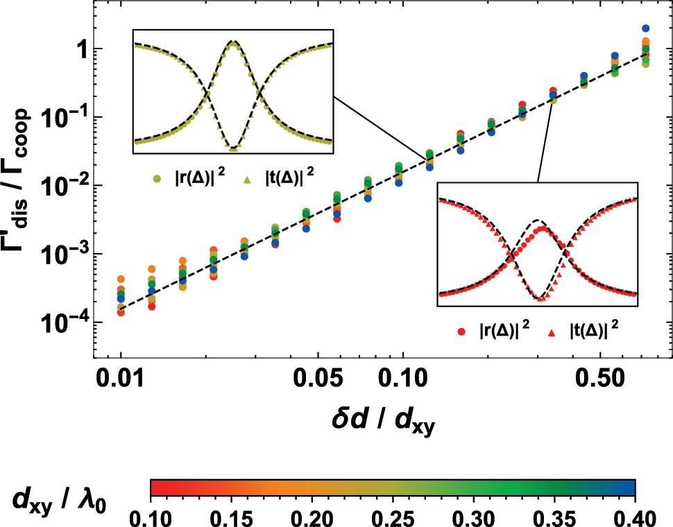
Average inelastic scattering due to the disorder in the atomic positions. For each value of the lattice constant d
x
= d
y
= d
xy
of a square, 2D array, we randomly displace the atomic positions within a sphere of radius δd. We then compute the average resonant reflection ⟨r⟩ at Δ = ω
coop, upon illumination by an input Gaussian beam of waist w
0 = L/4 ≥ λ
0, where L is the size of the array. Each point is obtained by averaging over 50 random sets of displaced positions. The value of L varied to keep the number of atomic emitters to N = 500. For each configuration, we define the inelastic rate from Eq. (A.2), as
Using Eq. (A.2) as an operative definition, we are able to estimate the value of
which is represented by a black, dashed line. The numerics confirm our intuition, proving that Eq. (A.3) describes well the reflection properties, at least as long as δd ≲ 0.7d
xy
and δd ≪ λ
0. From a similar analysis, we found that this prediction can capture the spectral behavior of both the reflection ⟨r(Δ)⟩ and the transmission ⟨t(Δ)⟩ coefficients as a function of the detuning (e.g., see the insets of Figure A.2, for the case with either d
xy
= 0.025λ
0 and δd ≈ 0.12d
xy
or d
xy
= 0.1λ
0 and δd ≈ 0.34d
xy
). The result in Eq. (A.3) should in principle be extendable to the case of rectangular arrays with d
x
≠ d
y
, by using the substitution rule
Appendix B: Evanescent interaction
In this appendix, we further investigate the role of evanescent interactions between 2D atomic arrays, with the goal of justifying the assumption that they are negligible in our regime of interest. We recall that we deal with rectangular, 2D arrays of constants d
x,y
≤ λ
0, placed at a distance of d
z
, and that the dipole matrix elements of the emitters are
where the diffraction orders are labeled by the integer numbers (a, b), which identify the corresponding wavevector
The evanescent interaction is stronger for nearest neighbor layers, so we focus on
Going beyond this rough estimate, in Figure A.3, we numerically calculate the ratio of evanescent to radiative interaction strength
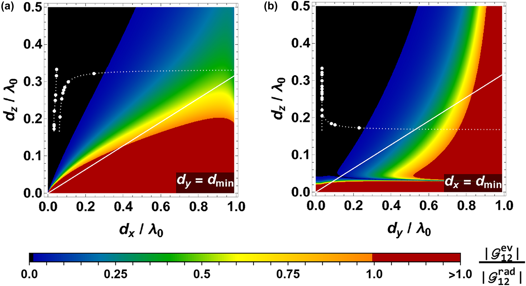
Strength of the evanescent interaction between two nearest neighbor layers of atoms. The color legend identifies the relative magnitude
These conclusions apply for all sets of lattice constants, excluding the limit of d y → λ 0. In that specific case, indeed, the diffraction order with (a, b) = (0, 1) would give rise, in Eq. (A.4), to a nominally infinite evanescent contribution arising from the constructive interference between an infinite number of atoms in each 2D layer, associated with an infinite range ξ 01 → ∞ of interaction.
Appendix C: Buffer zones
Here, we describe in detail our definition of the buffer zone between consecutive rings of an atomic metalens. This scheme explicitly takes advantage of the fact that, in our approach, often one of the two lattice constants d x,y does not change between two consecutive rings. The full algorithm is described below.
Given each ring j, its first 0 ≤ α < 1 fraction is reserved as a buffer zone (green and orange regions of Figure A.4), aimed to connect the array inside the j-th ring with the previous, in a smoother way. Hereafter, we describe how a generic j-th buffer (separating the (j − 1)-th and the j-th ring) is constructed.
First, the system checks if either
Let us assume that one has
In this regime, the lattices are organized in columns spaced by either
At this point, the algorithm counts the number of columns in either the j-th or the (j − 1)-th ring, satisfying the condition 0 ≤ x j,j−1 ≤ x max. Then, it identifies which of the two rings has less columns. For the sake of simplicity, we will assume it to be the j-th ring, but the algorithm deals with the opposite case in a similar manner. For each column i of this ring, the code searches the horizontally nearest column k among the ones of the (j − 1)-th ring, i.e., the one minimizing the quantity
Given this pair of columns, the algorithm connects them by drawing a straight line, and then placing atoms with a vertical spacing
For what concerns the
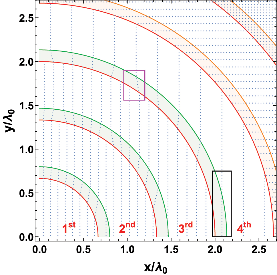
Example of “buffer zones” between two consecutive rings, in the
Appendix D: Definition of the efficiency
In our simulations of an atomic metalens, we consider a finite ensemble of N,
where
where one has
and
Here,
where we have
Here, we recall that
Appendix E: Spectral behavior of the metalens
We described a method to engineer an atomic metalens, designed to optimally focus resonant light Δ = ω − ω 0 = 0. Nonetheless, it is interesting to explore the bandwidth where the efficiency remains high. To address this question, we consider the illustrative example of the main text, corresponding to a metalens with focal length f = 20λ 0, radius R lens = 10λ 0, and constitutive parameters ΔR ≈ 2λ 0/3, ϕ 0 ≃ −2.06, and α ≈ 0.2, which acts on an input beam of waist w 0 = 4λ 0.
Intuitively, we expect the largest bandwidth of nonvanishing optical response to be of the same order of the maximum cooperative decay rate allowed in our system, i.e.,
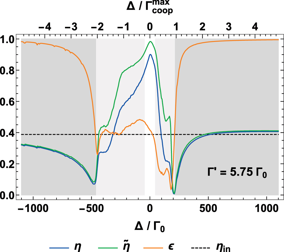
Spectral response of the atomic metalens, with focal length f = 20λ
0, radius R
lens = 10λ
0, and parameters ΔR ≈ 2λ
0/3, ϕ
0 ≃ −2.06, and α ≈ 0.2. The curves represent the efficiency η (blue), signal-to-background ratio
On the contrary, the behavior inside the light-gray area is irregular, but we can identify a bandwidth (white area) of
References
[1] M. Gross and S. Haroche, “Superradiance: an essay on the theory of collective spontaneous emission,” Phys. Rep., vol. 93, no. 5, pp. 301–396, 1982. https://doi.org/10.1016/0370-1573(82)90102-8.Search in Google Scholar
[2] A. S. Sheremet, et al.., “Waveguide quantum electrodynamics: collective radiance and photon-photon correlations,” Rev. Mod. Phys., vol. 95, no. 1, p. 015002, 2023. https://doi.org/10.1103/revmodphys.95.015002.Search in Google Scholar
[3] S. D. Jenkins and J. Ruostekoski, “Controlled manipulation of light by cooperative response of atoms in an optical lattice,” Phys. Rev. A, vol. 86, no. 3, p. 031602, 2012. https://doi.org/10.1103/physreva.86.031602.Search in Google Scholar
[4] G. Facchinetti, S. D. Jenkins, and J. Ruostekoski, “Storing light with subradiant correlations in arrays of atoms,” Phys. Rev. Lett., vol. 117, no. 24, p. 243601, 2016. https://doi.org/10.1103/physrevlett.117.243601.Search in Google Scholar PubMed
[5] A. Asenjo-Garcia, et al.., “Exponential improvement in photon storage fidelities using subradiance and “selective radiance” in atomic arrays,” Phys. Rev. X, vol. 7, no. 3, p. 31024, 2017. https://doi.org/10.1103/physrevx.7.031024.Search in Google Scholar
[6] J. Perczel, et al.., “Photonic band structure of two-dimensional atomic lattices,” Phys. Rev. A, vol. 96, no. 6, p. 063801, 2017. https://doi.org/10.1103/physreva.96.063801.Search in Google Scholar
[7] M. T. Manzoni, et al.., “Optimization of photon storage fidelity in ordered atomic arrays,” New J. Phys., vol. 20, no. 8, p. 83048, 2018. https://doi.org/10.1088/1367-2630/aadb74.Search in Google Scholar PubMed PubMed Central
[8] P. O. Guimond, et al.., “Subradiant bell states in distant atomic arrays,” Phys. Rev. Lett., vol. 122, no. 9, p. 093601, 2019. https://doi.org/10.1103/physrevlett.122.093601.Search in Google Scholar
[9] R. J. Bettles, et al.., “Quantum and nonlinear effects in light transmitted through planar atomic arrays,” Commun. Phys., vol. 3, no. 141, pp. 1–9, 2020. https://doi.org/10.1038/s42005-020-00404-3.Search in Google Scholar
[10] K. Brechtelsbauer and D. Malz, “Quantum simulation with fully coherent dipole-dipole interactions mediated by three-dimensional subwavelength atomic arrays,” Phys. Rev. A, vol. 104, no. 1, p. 013701, 2021. https://doi.org/10.1103/physreva.104.013701.Search in Google Scholar
[11] Z. Y. Wei, et al.., “Generation of photonic matrix product states with Rydberg atomic arrays,” Phys. Rev. Res., vol. 3, no. 2, p. 023021, 2021. https://doi.org/10.1103/physrevresearch.3.023021.Search in Google Scholar
[12] C. C. Rusconi, T. Shi, and J. I. Cirac, “Exploiting the photonic nonlinearity of free-space subwavelength arrays of atoms,” Phys. Rev. A, vol. 104, no. 3, p. 033718, 2021. https://doi.org/10.1103/physreva.104.033718.Search in Google Scholar
[13] T. L. Patti, et al.., “Controlling interactions between quantum emitters using atom arrays,” Phys. Rev. Lett., vol. 126, no. 22, p. 223602, 2021. https://doi.org/10.1103/physrevlett.126.223602.Search in Google Scholar
[14] E. Sierra, S. J. Masson, and A. Asenjo-Garcia, “Dicke superradiance in ordered lattices: dimensionality matters,” Phys. Rev. Res., vol. 4, no. 2, p. 023207, 2022. https://doi.org/10.1103/physrevresearch.4.023207.Search in Google Scholar
[15] S. J. Masson and A. Asenjo-Garcia, “Universality of Dicke superradiance in arrays of quantum emitters,” Nat. Commun., vol. 13, no. 2285, pp. 1–7, 2022. https://doi.org/10.1038/s41467-022-29805-4.Search in Google Scholar PubMed PubMed Central
[16] F. Andreoli, et al.., “The maximum refractive index of an atomic crystal – from quantum optics to quantum chemistry,” arXiv:2303.10998, 2023.Search in Google Scholar
[17] Y. Solomons, R. Ben-Maimon, and E. Shahmoon, “Universal approach for quantum interfaces with atomic arrays,” PRX Quantum, vol. 5, no. 2, p. 020329, 2024.10.1103/PRXQuantum.5.020329Search in Google Scholar
[18] M. Moreno-Cardoner, D. Goncalves, and D. Chang, “Quantum nonlinear optics based on two-dimensional rydberg atom arrays,” Phys. Rev. Lett., vol. 127, no. 26, p. 263602, 2021. https://doi.org/10.1103/physrevlett.127.263602.Search in Google Scholar PubMed
[19] O. Rubies-Bigorda, et al.., “Photon control and coherent interactions via lattice dark states in atomic arrays,” Phys. Rev. Res., vol. 4, no. 1, p. 013110, 2022. https://doi.org/10.1103/physrevresearch.4.013110.Search in Google Scholar
[20] K. E. Ballantine and J. Ruostekoski, “Subradiance-protected excitation spreading in the generation of collimated photon emission from an atomic array,” Phys. Rev. Res., vol. 2, no. 2, p. 023086, 2020. https://doi.org/10.1103/physrevresearch.2.023086.Search in Google Scholar
[21] K. E. Ballantine and J. Ruostekoski, “Quantum single-photon control, storage, and entanglement generation with planar atomic arrays,” PRX Quantum, vol. 2, no. 4, p. 040362, 2021. https://doi.org/10.1103/prxquantum.2.040362.Search in Google Scholar
[22] J. Ruostekoski, “Cooperative quantum-optical planar arrays of atoms,” Phys. Rev. A, vol. 108, no. 3, p. 030101, 2023. https://doi.org/10.1103/physreva.108.030101.Search in Google Scholar
[23] R. J. Bettles, S. A. Gardiner, and C. S. Adams, “Enhanced optical cross section via collective coupling of atomic dipoles in a 2D array,” Phys. Rev. Lett., vol. 116, no. 10, p. 103602, 2016. https://doi.org/10.1103/physrevlett.116.103602.Search in Google Scholar
[24] E. Shahmoon, et al.., “Cooperative resonances in light scattering from two-dimensional atomic arrays,” Phys. Rev. Lett., vol. 118, no. 11, p. 113601, 2017. https://doi.org/10.1103/physrevlett.118.113601.Search in Google Scholar
[25] J. Rui, et al.., “A subradiant optical mirror formed by a single structured atomic layer,” Nature, vol. 583, no. 7816, pp. 369–374, 2020. https://doi.org/10.1038/s41586-020-2463-x.Search in Google Scholar PubMed
[26] N. Nefedkin, M. Cotrufo, and A. Alù, “Nonreciprocal total cross section of quantum metasurfaces,” Nanophotonics, vol. 12, no. 3, pp. 589–606, 2023. https://doi.org/10.1515/nanoph-2022-0596.Search in Google Scholar PubMed PubMed Central
[27] R. Alaee, et al.., “Quantum metamaterials with magnetic response at optical frequencies,” Phys. Rev. Lett., vol. 125, no. 6, p. 063601, 2020. https://doi.org/10.1103/physrevlett.125.063601.Search in Google Scholar PubMed
[28] K. E. Ballantine and J. Ruostekoski, “Optical magnetism and huygens’ surfaces in arrays of atoms induced by cooperative responses,” Phys. Rev. Lett., vol. 125, no. 14, p. 143604, 2020. https://doi.org/10.1103/physrevlett.125.143604.Search in Google Scholar PubMed
[29] K. E. Ballantine, D. Wilkowski, and J. Ruostekoski, “Optical magnetism and wavefront control by arrays of strontium atoms,” Phys. Rev. Res., vol. 4, no. 3, p. 033242, 2022. https://doi.org/10.1103/physrevresearch.4.033242.Search in Google Scholar
[30] K. E. Ballantine and J. Ruostekoski, “Cooperative optical wavefront engineering with atomic arrays,” Nanophotonics, vol. 10, no. 7, pp. 1901–1909, 2021. https://doi.org/10.1515/nanoph-2021-0059.Search in Google Scholar
[31] B. X. Wang, et al.., “Design of metasurface polarizers based on two-dimensional cold atomic arrays,” Opt. Express, vol. 25, no. 16, pp. 18760–18773, 2017. https://doi.org/10.1364/oe.25.018760.Search in Google Scholar PubMed
[32] N. S. Baßler, et al.., “Linear optical elements based on cooperative subwavelength emitter arrays,” Opt. Express, vol. 31, no. 4, pp. 6003–6026, 2023. https://doi.org/10.1364/oe.476830.Search in Google Scholar
[33] N. S. Baßler, et al.., “Metasurface-based hybrid optical cavities for chiral sensing,” Phys. Rev. Lett., vol. 132, no. 4, p. 043602, 2024. https://doi.org/10.1103/physrevlett.132.043602.Search in Google Scholar
[34] J. Engelberg and U. Levy, “The advantages of metalenses over diffractive lenses,” Nat. Commun., vol. 11, no. 1991, 2020. https://doi.org/10.1038/s41467-020-15972-9.Search in Google Scholar PubMed PubMed Central
[35] W. T. Chen, A. Y. Zhu, and F. Capasso, “Flat optics with dispersion-engineered metasurfaces,” Nat. Rev. Mater., vol. 5, no. 8, pp. 604–620, 2020. https://doi.org/10.1038/s41578-020-0203-3.Search in Google Scholar
[36] Z. Li, et al.., “Atomic optical antennas in solids,” Nat. Photonics, vol. 18, no. 10, pp. 1113–1120, 2024. https://doi.org/10.1038/s41566-024-01456-5.Search in Google Scholar
[37] M. Zhou, et al.., “Optical metasurface based on the resonant scattering in electronic transitions,” ACS Photonics, vol. 4, no. 5, pp. 1279–1285, 2017. https://doi.org/10.1021/acsphotonics.7b00219.Search in Google Scholar
[38] L. Chomaz, et al.., “Absorption imaging of a quasi-two-dimensional gas: a multiple scattering analysis,” New J. Phys., vol. 14, no. 5, p. 055001, 2012. https://doi.org/10.1088/1367-2630/14/5/055001.Search in Google Scholar
[39] J. Javanainen, et al.., “Shifts of a resonance line in a dense atomic sample,” Phys. Rev. Lett., vol. 112, no. 11, 2014. https://doi.org/10.1103/physrevlett.112.113603.Search in Google Scholar
[40] J. Javanainen and J. Ruostekoski, “Light propagation beyond the mean-field theory of standard optics,” Opt. Express, vol. 24, no. 2, p. 993, 2016. https://doi.org/10.1364/oe.24.000993.Search in Google Scholar PubMed
[41] B. Zhu, et al.., “Light scattering from dense cold atomic media,” Phys. Rev. A, vol. 94, no. 2, p. 023612, 2016. https://doi.org/10.1103/physreva.94.023612.Search in Google Scholar
[42] N. J. Schilder, et al.., “Polaritonic modes in a dense cloud of cold atoms,” Phys. Rev. A, vol. 93, no. 6, p. 063835, 2016. https://doi.org/10.1103/physreva.93.063835.Search in Google Scholar
[43] N. J. Schilder, et al.., “Homogenization of an ensemble of interacting resonant scatterers,” Phys. Rev. A, vol. 96, no. 1, p. 013825, 2017. https://doi.org/10.1103/physreva.96.013825.Search in Google Scholar
[44] N. Schilder, et al.., “Near-resonant light scattering by a subwavelength ensemble of identical atoms,” Phys. Rev. Lett., vol. 124, no. 7, p. 073403, 2020. https://doi.org/10.1103/physrevlett.124.073403.Search in Google Scholar
[45] S. Jennewein, et al.., “Propagation of light through small clouds of cold interacting atoms,” Phys. Rev. A, vol. 94, no. 5, 2016, https://doi.org/10.1103/physreva.94.053828.Search in Google Scholar
[46] S. Jennewein, et al.., “Coherent scattering of near-resonant light by a dense, microscopic cloud of cold two-level atoms: experiment versus theory,” Phys. Rev. A, vol. 97, no. 5, 2018. https://doi.org/10.1103/physreva.97.053816.Search in Google Scholar
[47] L. Corman, et al.., “Transmission of near-resonant light through a dense slab of cold atoms,” Phys. Rev. A, vol. 96, no. 5, p. 53629, 2017. https://doi.org/10.1103/physreva.96.053629.Search in Google Scholar
[48] S. D. Jenkins, et al.., “Collective resonance fluorescence in small and dense atom clouds: comparison between theory and experiment,” Phys. Rev. A, vol. 94, no. 2, p. 023842, 2016. https://doi.org/10.1103/physreva.94.023842.Search in Google Scholar
[49] H. Dobbertin, R. Löw, and S. Scheel, “Collective dipole-dipole interactions in planar nanocavities,” Phys. Rev. A, vol. 102, no. 3, p. 031701, 2020. https://doi.org/10.1103/physreva.102.031701.Search in Google Scholar
[50] The codes are available at the Github repositories: https://github.com/frandreoli/atoms_optical_response (optical simulations) and https://github.com/frandreoli/optimization_atoms_metalens (metalens efficiency optimization). The optical simulations allow to reconstruct the field at any point in space and calculate reflection, transmission and optical efficiencies, for a set of atomic emitters at arbitrary positions, including those of an atomic metalens. The optimization toolbox can implement many different algorithms, with the particle swarm empirically outperforming the others.Search in Google Scholar
[51] D. Fattal, et al.., “Flat dielectric grating reflectors with focusing abilities,” Nat. Photonics, vol. 4, no. 7, pp. 466–470, 2010. https://doi.org/10.1038/nphoton.2010.116.Search in Google Scholar
[52] A. B. Klemm, et al.., “Experimental high numerical aperture focusing with high contrast gratings,” Opt. Lett., vol. 38, no. 17, p. 3410, 2013. https://doi.org/10.1364/ol.38.003410.Search in Google Scholar PubMed
[53] M. Khorasaninejad, et al.., “Metalenses at visible wavelengths: diffraction-limited focusing and subwavelength resolution imaging,” Science, vol. 352, no. 6290, pp. 1190–1194, 2016. https://doi.org/10.1126/science.aaf6644.Search in Google Scholar PubMed
[54] Z. Zhou, et al.., “Efficient silicon metasurfaces for visible light,” ACS Photonics, vol. 4, no. 3, pp. 544–551, 2017. https://doi.org/10.1021/acsphotonics.6b00740.Search in Google Scholar
[55] H. Liang, et al.., “Ultrahigh numerical aperture metalens at visible wavelengths,” Nano Lett., vol. 18, no. 7, pp. 4460–4466, 2018. https://doi.org/10.1021/acs.nanolett.8b01570.Search in Google Scholar PubMed
[56] A. V. Kildishev, A. Boltasseva, and V. M. Shalaev, “Planar photonics with metasurfaces,” Science, vol. 339, no. 6125, pp. 12320091–12320096, 2013. https://doi.org/10.1126/science.1232009.Search in Google Scholar PubMed
[57] N. Yu and F. Capasso, “Flat optics with designer metasurfaces,” Nat. Mater., vol. 13, no. 2, pp. 139–150, 2014. https://doi.org/10.1038/nmat3839.Search in Google Scholar PubMed
[58] W. T. Chen and F. Capasso, “Will flat optics appear in everyday life anytime soon?,” Appl. Phys. Lett., vol. 118, no. 10, p. 100503, 2021. https://doi.org/10.1063/5.0039885.Search in Google Scholar
[59] S. Shrestha, et al.., “Broadband achromatic dielectric metalenses,” Light Sci. Appl., vol. 7, no. 85, 2018. https://doi.org/10.1038/s41377-018-0078-x.Search in Google Scholar PubMed PubMed Central
[60] C. Bradac, et al.., “Quantum nanophotonics with group IV defects in diamond,” Nat. Commun., vol. 10, no. 5625, pp. 1–13, 2019. https://doi.org/10.1038/s41467-019-13332-w.Search in Google Scholar PubMed PubMed Central
[61] V. M. Acosta, et al.., “Diamonds with a high density of nitrogen-vacancy centers for magnetometry applications,” Phys. Rev. B, vol. 80, no. 11, 2009. https://doi.org/10.1103/physrevb.80.115202.Search in Google Scholar
[62] C. Hepp, et al.., “Electronic structure of the silicon vacancy color center in diamond,” Phys. Rev. Lett., vol. 112, no. 3, p. 036405, 2014. https://doi.org/10.1103/physrevlett.112.036405.Search in Google Scholar
[63] T. Müller, et al.., “Optical signatures of silicon-vacancy spins in diamond,” Nat. Commun., vol. 5, no. 3328, pp. 1–7, 2014. https://doi.org/10.1038/ncomms4328.Search in Google Scholar PubMed
[64] T. Iwasaki, et al.., “Tin-vacancy quantum emitters in diamond,” Phys. Rev. Lett., vol. 119, no. 25, p. 253601, 2017. https://doi.org/10.1103/physrevlett.119.253601.Search in Google Scholar PubMed
[65] M. E. Trusheim, et al.., “Lead-related quantum emitters in diamond,” Phys. Rev. B, vol. 99, no. 7, p. 075430, 2019. https://doi.org/10.1103/physrevb.99.075430.Search in Google Scholar
[66] J. M. Smith, et al.., “Colour centre generation in diamond for quantum technologies,” Nanophotonics, vol. 8, no. 11, pp. 1889–1906, 2019. https://doi.org/10.1515/nanoph-2019-0196.Search in Google Scholar
[67] K. Ohno, et al.., “Three-dimensional localization of spins in diamond using 12C implantation,” Appl. Phys. Lett., vol. 105, no. 5, p. 52406, 2014. https://doi.org/10.1063/1.4890613.Search in Google Scholar
[68] T. Y. Hwang, et al.., “Sub-10 nm precision engineering of solid-state defects via nanoscale aperture array mask,” Nano Lett., vol. 22, no. 4, pp. 1672–1679, 2022. https://doi.org/10.1021/acs.nanolett.1c04699.Search in Google Scholar PubMed
[69] J. Michl, et al.., “Perfect alignment and preferential orientation of nitrogen-vacancy centers during chemical vapor deposition diamond growth on (111) surfaces,” Appl. Phys. Lett., vol. 104, no. 10, p. 102407, 2014. https://doi.org/10.1063/1.4868128.Search in Google Scholar
[70] M. Lesik, et al.., “Perfect preferential orientation of nitrogen-vacancy defects in a synthetic diamond sample,” Appl. Phys. Lett., vol. 104, no. 11, p. 113107, 2014. https://doi.org/10.1063/1.4869103.Search in Google Scholar
[71] T. Fukui, et al.., “Perfect selective alignment of nitrogen-vacancy centers in diamond,” Appl. Phys. Express, vol. 7, no. 5, p. 055201, 2014. https://doi.org/10.7567/apex.7.055201.Search in Google Scholar
[72] H. Ozawa, et al.., “Formation of perfectly aligned nitrogen-vacancy-center ensembles in chemical-vapor-deposition-grown diamond (111),” Appl. Phys. Express, vol. 10, no. 4, p. 045501, 2017. https://doi.org/10.7567/apex.10.045501.Search in Google Scholar
[73] J. L. Pacheco, et al.., “Ion implantation for deterministic single atom devices,” Rev. Sci. Instrum., vol. 88, no. 12, 2017. https://doi.org/10.1063/1.5001520.Search in Google Scholar PubMed
[74] Y.-C. Chen, et al.., “Laser writing of individual nitrogen-vacancy defects in diamond with near-unity yield,” Optica, vol. 6, no. 5, pp. 662–667, 2019. https://doi.org/10.1364/optica.6.000662.Search in Google Scholar
[75] Y. Zhou, et al.., “Direct writing of single germanium vacancy center arrays in diamond,” New J. Phys., vol. 20, no. 12, p. 125004, 2018. https://doi.org/10.1088/1367-2630/aaf2ac.Search in Google Scholar
[76] D. Scarabelli, et al.., “Nanoscale engineering of closely-spaced electronic spins in diamond,” Nano Lett., vol. 16, no. 8, pp. 4982–4990, 2016. https://doi.org/10.1021/acs.nanolett.6b01692.Search in Google Scholar PubMed
[77] C. J. Stephen, et al.., “Deep three-dimensional solid-state qubit arrays with long-lived spin coherence,” Phys. Rev. Appl., vol. 12, no. 6, p. 064005, 2019. https://doi.org/10.1103/physrevapplied.12.064005.Search in Google Scholar
[78] X. Guo, et al.., “Tunable and transferable diamond membranes for integrated quantum technologies,” Nano Lett., vol. 21, no. 24, pp. 10392–10399, 2021. https://doi.org/10.1021/acs.nanolett.1c03703.Search in Google Scholar PubMed PubMed Central
[79] J. Ren, et al.., “Three-dimensional superlattice engineering with block copolymer epitaxy,” Sci. Adv., vol. 6, no. 24, 2020. https://doi.org/10.1126/sciadv.aaz0002.Search in Google Scholar PubMed PubMed Central
[80] F. Andreoli, et al.., “Maximum refractive index of an atomic medium,” Phys. Rev. X, vol. 11, no. 1, p. 011026, 2021. https://doi.org/10.1103/physrevx.11.011026.Search in Google Scholar
[81] L. Novotny and B. Hecht, Principles of Nano-Optics, Cambridge, Cambridge University Press, 2009.Search in Google Scholar
[82] M. Antezza and Y. Castin, “Spectrum of light in a quantum fluctuating periodic structure,” Phys. Rev. Lett., vol. 103, no. 12, p. 123903, 2009. https://doi.org/10.1103/physrevlett.103.123903.Search in Google Scholar PubMed
[83] M. Antezza and Y. Castin, “Fano-Hopfield model and photonic band gaps for an arbitrary atomic lattice,” Phys. Rev. A, vol. 80, no. 1, p. 013816, 2009. https://doi.org/10.1103/physreva.80.013816.Search in Google Scholar
[84] C.-R. Mann, et al.., “Selective radiance in super-wavelength atomic arrays,” arXiv:2402.06439, 2024.Search in Google Scholar
[85] R. Ben-Maimon, et al.., “Quantum interfaces with multilayered superwavelength atomic arrays,” arXiv:2402.06839, 2024.Search in Google Scholar
[86] S. P. Pedersen, L. Zhang, and T. Pohl, “Quantum nonlinear metasurfaces from dual arrays of ultracold atoms,” Phys. Rev. Res., vol. 5, no. 1, p. L012047, 2023. https://doi.org/10.1103/physrevresearch.5.l012047.Search in Google Scholar
[87] B. E. A. Saleh and M. C. Teich, Fundamentals of Photonics, New York, John Wiley & Sons, Inc., 1991.10.1002/0471213748Search in Google Scholar
[88] H. Zheng and H. U. Baranger, “Persistent quantum beats and long-distance entanglement from waveguide-mediated interactions,” Phys. Rev. Lett., vol. 110, no. 11, p. 113601, 2013. https://doi.org/10.1103/physrevlett.110.113601.Search in Google Scholar
[89] H. van de Stadt and J. M. Muller, “Multimirror Fabry–Perot interferometers,” JOSA A, vol. 2, no. 8, p. 1363, 1985. https://doi.org/10.1364/josaa.2.001363.Search in Google Scholar
[90] I. H. Deutsch, et al.., “Photonic band gaps in optical lattices,” Phys. Rev. A, vol. 52, no. 2, pp. 1394–1410, 1995. https://doi.org/10.1103/physreva.52.1394.Search in Google Scholar PubMed
[91] R. Menon and B. Sensale-Rodriguez, “Inconsistencies of metalens performance and comparison with conventional diffractive optics,” Nat. Photonics, vol. 17, no. 11, pp. 923–924, 2023. https://doi.org/10.1038/s41566-023-01306-w.Search in Google Scholar
[92] J. Bezanson, et al.., “Julia: a fresh approach to numerical computing,” SIAM Rev., vol. 59, no. 1, pp. 65–98, 2017. https://doi.org/10.1137/141000671.Search in Google Scholar
[93] R. E. Evans, et al.., “Narrow-linewidth homogeneous optical emitters in diamond nanostructures via silicon ion implantation,” Phys. Rev. Appl., vol. 5, no. 4, p. 044010, 2016. https://doi.org/10.1103/physrevapplied.5.044010.Search in Google Scholar
[94] T. Schröder, et al.., “Scalable focused ion beam creation of nearly lifetime-limited single quantum emitters in diamond nanostructures,” Nat. Commun., vol. 8, no. 15376, pp. 1–7, 2017. https://doi.org/10.1038/ncomms15376.Search in Google Scholar PubMed PubMed Central
[95] M. Pan, et al.., “Dielectric metalens for miniaturized imaging systems: progress and challenges,” Light Sci. Appl., vol. 11, no. 195, pp. 1–32, 2022. https://doi.org/10.1038/s41377-022-00885-7.Search in Google Scholar PubMed PubMed Central
[96] L. Huang, S. Zhang, and T. Zentgraf, “Metasurface holography: from fundamentals to applications,” Nanophotonics, vol. 7, no. 6, pp. 1169–1190, 2018. https://doi.org/10.1515/nanoph-2017-0118.Search in Google Scholar
[97] C. M. Lalau-Keraly, et al.., “Adjoint shape optimization applied to electromagnetic design,” Opt. Express, vol. 21, no. 18, pp. 21693–21701, 2013. https://doi.org/10.1364/oe.21.021693.Search in Google Scholar PubMed
[98] R. Paniagua-Domínguez, et al.., “A metalens with a near-unity numerical aperture,” Nano Lett., vol. 18, no. 3, pp. 2124–2132, 2018. https://doi.org/10.1021/acs.nanolett.8b00368.Search in Google Scholar PubMed
[99] R. E. Christiansen, et al.., “Inverse design of nanoparticles for enhanced Raman scattering,” Opt. Express, vol. 28, no. 4, pp. 4444–4462, 2020. https://doi.org/10.1364/oe.28.004444.Search in Google Scholar PubMed
[100] H. Chung and O. D. Miller, “High-NA achromatic metalenses by inverse design,” Opt. Express, vol. 28, no. 5, pp. 6945–6965, 2020. https://doi.org/10.1364/oe.385440.Search in Google Scholar
[101] O. A. Abdelraouf, et al.., “Recent advances in tunable metasurfaces: materials, design, and applications,” ACS Nano, vol. 16, no. 9, pp. 13339–13369, 2022. https://doi.org/10.1021/acsnano.2c04628.Search in Google Scholar PubMed
[102] I. Volkov, et al.., “Non-radiative configurations of a few quantum emitters ensembles: evolutionary optimization approach,” Appl. Phys. Lett., vol. 124, no. 8, 2024. https://doi.org/10.1063/5.0189405.Search in Google Scholar
[103] O. D. Miller, “Photonic design: from fundamental solar cell physics to computational inverse design,” arXiv:1308.0212, 2013.Search in Google Scholar
[104] M. S. Bin-Alam, et al.., “Ultra-high-Q resonances in plasmonic metasurfaces,” Nat. Commun., vol. 12, no. 974, pp. 1–8, 2021. https://doi.org/10.1038/s41467-021-21196-2.Search in Google Scholar PubMed PubMed Central
[105] K. Shastri and F. Monticone, “Nonlocal flat optics,” Nat. Photonics, vol. 17, no. 1, pp. 36–47, 2022. https://doi.org/10.1038/s41566-022-01098-5.Search in Google Scholar
[106] C. Chen, et al.., “Spectral tomographic imaging with aplanatic metalens,” Light Sci. Appl., vol. 8, no. 1, pp. 1–8, 2019. https://doi.org/10.1038/s41377-019-0208-0.Search in Google Scholar PubMed PubMed Central
[107] A. Arbabi, et al.., “Subwavelength-thick lenses with high numerical apertures and large efficiency based on high-contrast transmitarrays,” Nat. Commun., vol. 6, no. 1, pp. 1–6, 2015. https://doi.org/10.1038/ncomms8069.Search in Google Scholar PubMed
[108] A. McClung, et al.., “Snapshot spectral imaging with parallel metasystems,” Sci. Adv., vol. 6, no. 38, pp. 7646–7664, 2020. https://doi.org/10.1126/sciadv.abc7646.Search in Google Scholar PubMed PubMed Central
[109] J. van de Groep, et al.., “Exciton resonance tuning of an atomically thin lens,” Nat. Photonics, vol. 14, no. 7, pp. 426–430, 2020. https://doi.org/10.1038/s41566-020-0624-y.Search in Google Scholar
[110] K. Ou, et al.., “Mid-infrared polarization-controlled broadband achromatic metadevice,” Sci. Adv., vol. 6, no. 37, pp. 711–722, 2020. https://doi.org/10.1126/sciadv.abc0711.Search in Google Scholar PubMed PubMed Central
[111] S. Gao, et al.., “Twofold polarization-selective all-dielectric trifoci metalens for linearly polarized visible light,” Adv. Opt. Mater., vol. 7, no. 21, p. 1900883, 2019. https://doi.org/10.1002/adom.201900883.Search in Google Scholar
[112] J. Ma, et al.., “Engineering quantum light sources with flat optics,” Adv. Mater., p. 2313589, 2024, https://doi.org/10.1002/adma.202313589.Search in Google Scholar PubMed
[113] A. S. Solntsev, G. S. Agarwal, and Y. Y. Kivshar, “Metasurfaces for quantum photonics,” Nat. Photonics, vol. 15, no. 5, pp. 327–336, 2021. https://doi.org/10.1038/s41566-021-00793-z.Search in Google Scholar
[114] J.-Z. Yang, et al.., “Quantum metasurface holography,” Photonics Res., vol. 10, no. 11, pp. 2607–2613, 2022. https://doi.org/10.1364/prj.470537.Search in Google Scholar
[115] Q. Y. Wu, et al.., “Quantum process tomography on holographic metasurfaces,” Npj Quantum Inf., vol. 8, no. 46, pp. 1–6, 2022. https://doi.org/10.1038/s41534-022-00561-z.Search in Google Scholar
[116] L. J. Rogers, et al.., “Electronic structure of the negatively charged silicon-vacancy center in diamond,” Phys. Rev. B, vol. 89, no. 23, p. 235101, 2014. https://doi.org/10.1103/physrevb.89.235101.Search in Google Scholar
[117] K. D. Jahnke, et al.., “Electron-phonon processes of the silicon-vacancy centre in diamond,” New J. Phys., vol. 17, no. 4, p. 043011, 2015. https://doi.org/10.1088/1367-2630/17/4/043011.Search in Google Scholar
[118] D. D. Sukachev, et al.., “Silicon-vacancy spin qubit in diamond: a quantum memory exceeding 10 ms with single-shot state readout,” Phys. Rev. Lett., vol. 119, no. 22, p. 223602, 2017. https://doi.org/10.1103/physrevlett.119.223602.Search in Google Scholar PubMed
[119] A. Sipahigil, et al.., “Indistinguishable photons from separated silicon-vacancy centers in diamond,” Phys. Rev. Lett., vol. 113, no. 11, p. 113602, 2014. https://doi.org/10.1103/physrevlett.113.113602.Search in Google Scholar
[120] L. J. Rogers, et al.., “Multiple intrinsically identical single-photon emitters in the solid state,” Nat. Commun., vol. 5, 2014, https://doi.org/10.1038/ncomms5739.Search in Google Scholar PubMed
[121] P. Wang, et al.., “Transform-limited photon emission from a lead-vacancy center in diamond above 10 K,” Phys. Rev. Lett., vol. 132, no. 7, p. 073601, 2024. https://doi.org/10.1103/physrevlett.132.073601.Search in Google Scholar PubMed
[122] L. Novotny and N. Van Hulst, “Antennas for light,” Nat. Photonics, vol. 5, no. 2, pp. 83–90, 2011. https://doi.org/10.1038/nphoton.2010.237.Search in Google Scholar
© 2025 the author(s), published by De Gruyter, Berlin/Boston
This work is licensed under the Creative Commons Attribution 4.0 International License.
Articles in the same Issue
- Frontmatter
- Review
- Dielectric metasurface-assisted terahertz sensing: mechanism, fabrication, and multiscenario applications
- Research Articles
- General design flow for waveguide Bragg gratings
- High-efficiency radiation beyond the critical angle via phase-gradient antireflection metasurfaces
- Collision of high-resolution wide FOV metalens cameras and vision tasks
- Waveguide-integrated spatial mode filters with PtSe2 nanoribbons
- Nanoscale resolved mapping of the dipole emission of hBN color centers with a scattering-type scanning near-field optical microscope
- Dynamically tunable robust ultrahigh-Q merging bound states in the continuum in phase-change materials metasurface
- Ultrafast pulse propagation time-domain dynamics in dispersive one-dimensional photonic waveguides
- A programmable platform for photonic topological insulators
- Metalens formed by structured arrays of atomic emitters
- Realizing electronically reconfigurable intrinsic chirality: from no absorption to maximal absorption of any desirable spin
- A general model for designing the chirality of exciton-polaritons
- Simultaneous control of three degrees of freedom in perfect vector vortex beams based on metasurfaces