Overcoming stress limitations in SiN nonlinear photonics via a bilayer waveguide
-
Karl J. McNulty

 ,
Shriddha Chaitanya
,
Swarnava Sanyal
,
Andres Gil-Molina
,
Mateus Corato-Zanarella
,
Yoshitomo Okawachi
,
Alexander L. Gaeta
und
Michal Lipson
,
Shriddha Chaitanya
,
Swarnava Sanyal
,
Andres Gil-Molina
,
Mateus Corato-Zanarella
,
Yoshitomo Okawachi
,
Alexander L. Gaeta
und
Michal Lipson

Abstract
Silicon nitride (SiN) formed via low pressure chemical vapor deposition (LPCVD) is an ideal material platform for on-chip nonlinear photonics owing to its low propagation loss and competitive nonlinear index. Despite this, LPCVD SiN is restricted in its scalability due to the film stress when high thicknesses, required for nonlinear dispersion engineering, are deposited. This stress in turn leads to film cracking and makes integrating such films in silicon foundries challenging. To overcome this limitation, we propose a bilayer waveguide scheme comprised of a thin LPCVD SiN layer underneath a low-stress and low-index PECVD SiN layer. We show group velocity dispersion tuning at 1,550 nm without concern for film-cracking while enabling low loss resonators with intrinsic quality factors above 1 million. Finally, we demonstrate a locked, normal dispersion Kerr frequency comb with our bilayer waveguide resonators spanning 120 nm in the c-band with an on-chip pump power of 350 mW.
1 Introduction
Low pressure chemical vapor deposition (LPCVD) silicon nitride (SiN) films have emerged as an ideal candidate for optical non-linear applications, owing to SiN’s low optical loss and high n 2 value [1]. Despite the desirable characteristics, LPCVD SiN waveguides often require thick films (>400 nm) to satisfy the group velocity dispersion (GVD) requirements for nonlinear processes in the telecom range. Such thick SiN films are plagued by high tensile stress and subsequent film cracking, thereby lowering the photonic device yield and limiting their applicability in large-scale systems. Figure 1a shows the simulated GVD for an LPCVD SiN waveguide with a 1.5 μm width and various heights. As an example of dispersion needed for nonlinear processes, we highlight the dispersion range that facilitates comb formation in the telecom wavelength range [2], [3], [4], [5], [6], [7], [8], [9], [10], [11]. As Figure 1a indicates, the waveguide GVD in the c-band only reaches the target normal and anomalous GVD range when the waveguide thickness is beyond 500 nm, above the typical thickness limit of 400 nm in foundries [12]. Figure 1b shows an example of the extreme cracking in 700 nm SiN film which forms at the edge of a 100 mm wafer (right) and propagates to the center of the wafer (left). Such cracking is almost unavoidable in LPCVD SiN films above the thickness threshold of 400 nm and is a key limiting factor of wider integration of SiN based nonlinear photonics.
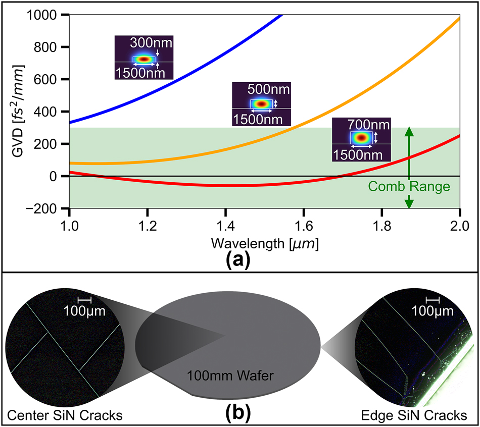
Thickness dependent waveguide dispersion and film cracking in SiN. (a) Dispersion comparison of a 1.5 μm wide LPCVD SiN waveguide with various thicknesses. The green shaded area indicates a general GVD range which has been shown to generate microcombs. (b) Visible film cracking seen under a dark field microscope of a 730 nm thick LPCVD SiN film on a 100 mm wafer. Cracks propagate from the edge of a wafer (right) and pass through the center of the wafer (left).
To mitigate the material stress limitation, fabrication approaches consist of stress relief trenches prior to SiN deposition [13], [14], [15], [16], [17], [18] or the use of chemical mechanical planarization (CMP) for a photonic damascene process [19], [20], [21]. Stress relief trenches take up valuable wafer area leading to potential compromises in device density. High film stress at large thicknesses can also cause cracking to occur at the trench locations, making such trenches not always reliable against cracking (see Supplementary material). Although the damascene process has been scaled to 200 mm wafer sizes, it is hindered by variation in height from CMP and variation in width from thermal reflow processing steps. As such, waveguide dimensions and coupling gap sizes may be difficult to control leading to inaccurate waveguide dispersion and coupling [22]. Thermal cycling throughout deposition may also be employed to overcome cracking once LPCVD films surpass 400 nm in thickness. However, this has only recently been scaled to 150 mm wafers [14], and the cycled anneal steps lead to intermediate layers within the LPCVD SiN. Circumventing LPCVD SiN through the use of sputtered SiN [23], [24], [25], PECVD SiN [26], and deuterated PECVD SiN [27], [28], [29], [30] for stress-free, nonlinear devices has also been shown. In particular, deuterated PECVD SiN is a promising new platform for SiN based nonlinear technology as it provides a path towards low-loss resonators with low temperature depositions. The tools and gases required for deuterated PECVD SiN are expensive though, making deuterated PECVD films far less available compared to normal PECVD SiN. Additionally, deuterated SiN resonators, and all other high confinement methods, have not reached the lowest levels of loss achieved via LPCVD SiN processes [22], [31], [32].
Thin LPCVD SiN films below 400 nm, in contrast to thick LPCVD SiN films, do not suffer from stress and are readily available in foundries. Nonlinear processes may be realized with such thin films via mode crossing techniques [33], [34], [35]. However, devices based on thinner nitride films lack high modal confinement and the ability for broadband dispersion engineering [36].
Here we endow a foundry compatible, thin film LPCVD SiN with the desired GVD via a stress-free bilayer waveguide configuration. Shown in Figure 2b, we deposit a low index PECVD SiN (index of 1.78 at 1,550 nm) on a thin film of LPCVD SiN. The low index SiN layer enables stress free tuning of the overall dispersion of the composite waveguide, while maintaining low loss for the whole composite waveguide. It also ensures high modal overlap with the bottom LPCVD SiN to utilize its higher nonlinearity as the low index SiN is less dense and, therefore, has a lower relative n 2 [37] (see Supplementary material for film details). As our fabrication is subtractive and the film cracking is addressed via a bilayer film stack, our design offers the simplest approach to fabrication of dispersion engineered SiN waveguides. There is no concern for dishing or waveguide dimension variations from CMP and thermal reflow, nor need for stress-relief trenches which can limit device density and may not completely prevent cracking. Moreover, although we select a top film with a large index contrast to demonstrate the robustness of the approach, our method is adaptable to other variants of SiN films for the top layer including deuterated PECVD SiN. As an example of application, we use our bilayer waveguides to construct dual resonators, depicted in Figure 2a, which are commonly used for comb generation [10]. We choose a waveguide width of 1700 nm for our design, an LPCVD SiN layer of 340 nm in thickness, and a low index SiN layer of 400 nm in thickness. As Figure 2c shows, our design allows significant control over the waveguide GVD compared to the unaided thin LPCVD SiN waveguide of the same width. From dispersion simulations, the bilayer waveguide exhibits a GVD within the c-band sufficiently low to where normal GVD SiN microcombs have been demonstrated [2], [4], [5], [6], [7], [10]. In contrast we see that the 340 nm thick LPCVD SiN waveguide exhibits very high normal GVD and fails to reach the generally required dispersion for microcomb generation.

Bilayer waveguide design and dispersion. (a) 3D rendering of the bilayer design consisting of dual ring resonators and on-chip heaters for resonance detuning control. (b) Cross-section of the 1700 nm × 740 nm waveguide along with an overlay of the optical mode. (c) Waveguide GVD comparison of an unaided 1700 nm × 340 nm LPCVD SiN waveguide with that of the bilayer design. The addition of the low index SiN layer brings the dispersion down within the range of demonstrated combs without the tradeoff of high film stress.
2 Results and discussion
We experimentally validate that our waveguide design enables low loss resonators comparable to the loss levels of single-core LPCVD SiN resonators. To directly compare device loss, we fabricate identical single ring resonators with (a) standard 730 nm thick LPCVD SiN waveguides, (b) our bilayer waveguides with the thicknesses specified earlier, and (c) 730 nm thick low index SiN only waveguides. To fabricate the 730 nm thick LPCVD waveguides for comparison, we follow the trench and thermal annealing techniques detailed in [16]. We choose the ring radius to be 150 μm and the waveguide width to be 2000 nm for all devices tested. To minimize difference in performance attributed to process variation, these waveguides receive the same process steps and are fabricated in parallel with each other. For loss characterization, we selected one undercoupled ring for each waveguide type and measured roughly 50 resonances across a spectrum of 1,500 nm–1,600 nm. We then employ a coupled mode model with backscattering [38] to fit each individual resonance and extract the intrinsic quality factor as a measurement of cavity loss. Figure 3 shows a histogram of the fitted intrinsic quality factors for each device spectrum. Despite being composed of films of considerably different indices, our bilayer waveguides exhibit only a slight drop in loss compared to LPCVD SiN waveguides and retain intrinsic quality factors well above 1 million across the c-band. This is in stark comparison to the single-core, low index SiN waveguide which has much lower intrinsic quality factors in the range of 100 k - 600 k. Thus, our dispersion tuning design maintains low optical loss while not suffering from film stress.

Intrinsic quality factors for resonators of each waveguide type. (a) Histogram of the fitted intrinsic quality factors measured across a spectrum of 1,500 nm–1,600 nm for three separate ring resonator devices (0.2 million bin width). All three rings are 150 μm in radius and have cross-sections of 2000 nm × 730 nm. From left to right; the average intrinsic quality factors are 425 thousand, 2.23 million, and 3.04 million, corresponding to average loss rates of approximately 72.7 dB/m, 14.8 dB/m, and 11.1 dB/m, respectively. (b) Sample resonance fits for each of the different rings.
To demonstrate the practicality of our bilayer approach for nonlinear photonic applications, we demonstrate a low-noise, Kerr frequency comb spanning approximately 120 nm with 350 mW of on-chip pump power. As our bilayer waveguide has GVD shown in Figure 2b, we employ the dual ring configuration, as mentioned above, to enable comb generation in the normal dispersion regime. For our comb device, we choose a width of 1700 nm for our bilayer waveguide with a main ring of radius 120 μm and an auxiliary ring of radius 117 μm (as shown in Figure 2a). Pumping around 1,557 nm and following [10], we utilize our fully integrated, on-chip microheaters to tune the main ring and auxiliary ring frequency detunings and navigate to a low noise comb state. Figure 4 shows both the unlocked state (top) prior to tuning the microheater currents, and the low-noise, locked state (bottom) of the comb after tuning the microheater currents. Once locked, we observe the characteristic low RF frequency noise associated with such a locked state [39], in contrast to the high RF frequency noise seen in the unlocked state.

Low noise frequency comb generation in a bilayer waveguide resonator. (a) Optical spectrum analyzer (OSA) spectrum of the unlocked (top) and locked (bottom) comb states of our bilayer waveguide resonator (normalized to the pump line). (b) Associated RF frequency noise measured via an electrical spectrum analyzer (ESA).
3 Conclusions
Our approach to dispersion engineering provides a solution to the film stress plaguing SiN technology. By decoupling the waveguide dispersion from the thickness of a single LPCVD SiN layer, we enable dispersion engineered devices with low optical loss and without large film stress during fabrication. We generate coherent, low-noise combs using our new waveguide design and show that our approach is compatible with mode crossing techniques previously used for microcomb generation. Moreover, this approach is adaptable to other materials, as various PECVD Si x N y films or possibly TiO2 could be utilized as the dispersion tuning top layer.
4 Fabrication methods
We fabricate our devices starting from 100 mm wafers with 4 μm of wet thermal oxide. We then deposit the 340 nm of bottom SiN via LPCVD and follow this by depositing the 400 nm layer of low index SiN via PECVD. The LPCVD SiN film is deposited at 800 °C using a mixture of NH3 and DCS (SiH2Cl2). The PECVD top film is deposited at 350 °C, and we select an appropriate gas mixture of NH3, SiH4, and N2 which yields our low index film. We utilize an oxide hardmask alongside electron beam lithography to define our waveguides and etch them with a plasma dry etch. The waveguides are then annealed in an argon environment for 3 h and subsequently clad with a high temperature silicon dioxide. The platinum heaters are defined on the cladding oxide through a lift off process, and we perform a final deep silicon etch prior to dicing to enable low loss edge couplers. More details of our fabrication can be found in [40].
Funding source: Defense Advanced Research Projects Agency
Award Identifier / Grant number: HR00112420368
Funding source: Air Force Office of Scientific Research
Award Identifier / Grant number: FA9550-20-1-0297
Acknowledgement
The photonic chip fabrication was done in part at the Columbia Nano Initiative (CNI) Shared Lab Facilities at Columbia University, and in part at the Cornell NanoScale Facility, a member of the National Nanotechnology Coordinated Infrastructure (NNCI), which is supported by the National Science Foundation (Grant NNCI-2025233). The authors also acknowledge the use of the Nanofabrication Facility at the Advanced Science Research Center at The Graduate Center of City University of New York.
-
Research funding: The authors acknowledge the financial support of the Air Force Office of Scientific Research under grant FA9550-20-1-0297 and the Defense Advanced Research Projects Agency (DARPA) under grant HR00112420368.
-
Author contributions: KJM, YO, ALG, and ML conceived the idea. KJM did the planning and execution of the experiment including design, simulations, fabrication, testing, and data analysis. SC aided in film deposition. SS, AGM, and MCZ aided in device testing. KJM and ML wrote the manuscript. Edits were provided by all authors. All authors have accepted responsibility for the entire content of this manuscript and approved its submission.
-
Conflict of interest: Authors state no conflict of interest.
-
Data availability: Data underlying the results are presented throughout the paper and its Supplemental Information, and additional data may be obtained from the authors upon reasonable request.
References
[1] C. J. Krückel, A. Fülöp, Z. Ye, P. A. Andrekson, and V. Torres-Company, “Optical bandgap engineering in nonlinear silicon nitride waveguides,” Opt. Express, vol. 25, no. 13, pp. 15370–15380, 2017, https://doi.org/10.1364/oe.25.015370.Suche in Google Scholar
[2] Y. Okawachi, B. Y. Kim, J. K. Jang, X. Ji, M. Lipson, and A. L. Gaeta, “Broadband dual-pumped normal-GVD Kerr combs,” in 2021 Conference on Lasers and Electro-Optics (CLEO), 2021, pp. 1–2.10.1364/CLEO_SI.2021.SW4A.4Suche in Google Scholar
[3] T. J. Kippenberg, A. L. Gaeta, M. Lipson, and M. L. Gorodetsky, “Dissipative Kerr solitons in optical microresonators,” Science, vol. 361, no. 6402, p. eaan8083, 2018, https://doi.org/10.1126/science.aan8083.Suche in Google Scholar PubMed
[4] Y. Zhang, S. Zhang, T. Bi, and P. Del’Haye, “Geometry optimization for dark soliton combs in thin multimode silicon nitride microresonators,” Opt. Express, vol. 31, no. 25, pp. 41420–41427, 2023, https://doi.org/10.1364/oe.503637.Suche in Google Scholar PubMed
[5] Y. Liu, et al.., “Investigation of mode coupling in normal-dispersion silicon nitride microresonators for Kerr frequency comb generation,” Optica, vol. 1, no. 3, pp. 137–144, 2014, https://doi.org/10.1364/optica.1.000137.Suche in Google Scholar
[6] X. Xue, et al.., “Mode-locked dark pulse Kerr combs in normal-dispersion microresonators,” Nat. Photonics, vol. 9, no. 9, pp. 594–600, 2015, https://doi.org/10.1038/nphoton.2015.137.Suche in Google Scholar
[7] X. Xue, M. Qi, and A. M. Weiner, “Normal-dispersion microresonator Kerr frequency combs,” Nanophotonics, vol. 5, no. 2, pp. 244–262, 2016, https://doi.org/10.1515/nanoph-2016-0016.Suche in Google Scholar
[8] Y. Okawachi, K. Saha, J. S. Levy, Y. H. Wen, M. Lipson, and A. L. Gaeta, “Octave-spanning frequency comb generation in a silicon nitride chip,” Opt. Lett., vol. 36, no. 17, pp. 3398–3400, 2011, https://doi.org/10.1364/ol.36.003398.Suche in Google Scholar
[9] A. L. Gaeta, M. Lipson, and T. J. Kippenberg, “Photonic-chip-based frequency combs,” Nat. Photonics, vol. 13, no. 3, pp. 158–169, 2019, https://doi.org/10.1038/s41566-019-0358-x.Suche in Google Scholar
[10] B. Y. Kim, et al.., “Turn-key, high-efficiency Kerr comb source,” Opt. Lett., vol. 44, no. 18, pp. 4475–4478, 2019, https://doi.org/10.1364/ol.44.004475.Suche in Google Scholar
[11] T. Herr, et al.., “Universal formation dynamics and noise of Kerr-frequency combs in microresonators,” Nat. Photonics, vol. 6, no. 7, pp. 480–487, 2012, https://doi.org/10.1038/nphoton.2012.127.Suche in Google Scholar
[12] C. G. H. Roeloffzen, et al.., “Low-loss Si3N4 TriPleX optical waveguides: technology and applications overview,” IEEE J. Sel. Top. Quantum Electron., vol. 24, no. 4, pp. 1–21, 2018, https://doi.org/10.1109/jstqe.2018.2793945.Suche in Google Scholar
[13] R. M. Grootes, M. Dijkstra, Y. Klaver, D. Marpaung, and H. L. Offerhaus, “Crack barriers for thick SiN using dicing,” Opt. Express, vol. 30, no. 10, pp. 16725–16733, 2022, https://doi.org/10.1364/oe.456834.Suche in Google Scholar
[14] Z. Ye, et al.., “Foundry manufacturing of tight-confinement, dispersion-engineered, ultralow-loss silicon nitride photonic integrated circuits,” Photon. Res., vol. 11, no. 4, pp. 558–568, 2023, https://doi.org/10.1364/prj.486379.Suche in Google Scholar
[15] A. Gondarenko, J. S. Levy, and M. Lipson, “High confinement micron-scale silicon nitride high Q ring resonator,” Opt. Express, vol. 17, no. 14, pp. 11366–11370, 2009, https://doi.org/10.1364/oe.17.011366.Suche in Google Scholar PubMed
[16] K. Luke, A. Dutt, C. B. Poitras, and M. Lipson, “Overcoming Si3N4 film stress limitations for high quality factor ring resonators,” Opt. Express, vol. 21, no. 19, pp. 22829–22833, 2013, https://doi.org/10.1364/oe.21.022829.Suche in Google Scholar
[17] K. Wu and A. W. Poon, “Stress-released Si3N4 fabrication process for dispersion-engineered integrated silicon photonics,” Opt. Express, vol. 28, no. 12, pp. 17708–17722, 2020, https://doi.org/10.1364/oe.390171.Suche in Google Scholar PubMed
[18] H. E. Dirani, et al.., “Ultralow-loss tightly confining Si3N4 waveguides and high-Q microresonators,” Opt. Express, vol. 27, no. 21, pp. 30726–30740, 2019, https://doi.org/10.1364/oe.27.030726.Suche in Google Scholar
[19] M. H. P. Pfeiffer, et al.., “Photonic Damascene process for integrated high-Q microresonator based nonlinear photonics,” Optica, vol. 3, no. 1, pp. 20–25, 2016, https://doi.org/10.1364/optica.3.000020.Suche in Google Scholar
[20] M. H. P. Pfeiffer, J. Liu, A. S. Raja, T. Morais, B. Ghadiani, and T. J. Kippenberg, “Ultra-smooth silicon nitride waveguides based on the Damascene reflow process: fabrication and loss origins,” Optica, vol. 5, no. 7, pp. 884–892, 2018, https://doi.org/10.1364/optica.5.000884.Suche in Google Scholar
[21] J. Liu, et al.., “High-yield, wafer-scale fabrication of ultralow-loss, dispersion-engineered silicon nitride photonic circuits,” Nat. Commun., vol. 12, no. 1, p. 2236, 2021, https://doi.org/10.1038/s41467-021-21973-z.Suche in Google Scholar PubMed PubMed Central
[22] X. Ji, R. Ning Wang, Y. Liu, J. Riemensberger, Z. Qiu, and T. J. Kippenberg, “Efficient mass manufacturing of high-density, ultra-low-loss Si3N4 photonic integrated circuits,” Optica, vol. 11, no. 10, pp. 1397–1407, 2024, https://doi.org/10.1364/optica.529673.Suche in Google Scholar
[23] S. Zhang, et al.., “Low-temperature sputtered ultralow-loss silicon nitride for hybrid photonic integration,” Laser Photon. Rev., p. 2300642, 2024, [Online]. Available from: https://onlinelibrary.wiley.com/doi/abs/10.1002/lpor.202300642.10.1002/lpor.202300642Suche in Google Scholar
[24] S. Zhang, et al.., “Room-temperature sputtered ultralow-loss silicon nitride,” in 2023 Conference on Lasers and Electro-Optics Europe & European Quantum Electronics Conference (CLEO/Europe-EQEC), 2023, p. 1. [Online]. Available from: https://ieeexplore.ieee.org/abstract/document/10232644.10.1109/CLEO/Europe-EQEC57999.2023.10232644Suche in Google Scholar
[25] A. Frigg, et al.., “Optical frequency comb generation with low temperature reactive sputtered silicon nitride waveguides,” APL Photonics, vol. 5, no. 1, p. 011302, 2020. https://doi.org/10.1063/1.5136270.Suche in Google Scholar
[26] X. Ji, et al.., “Ultra-low-loss silicon nitride photonics based on deposited films compatible with foundries,” Laser Photon. Rev., vol. 17, no. 3, p. 2200544, 2023, https://doi.org/10.1002/lpor.202200544.Suche in Google Scholar
[27] J. Chiles, et al.., “Deuterated silicon nitride photonic devices for broadband optical frequency comb generation,” Opt. Lett., vol. 43, no. 7, pp. 1527–1530, 2018, https://doi.org/10.1364/ol.43.001527.Suche in Google Scholar
[28] Z. Wu, et al.., “Low-noise Kerr frequency comb generation with low temperature deuterated silicon nitride waveguides,” Opt. Express, vol. 29, no. 18, pp. 29557–29566, 2021, https://doi.org/10.1364/oe.438436.Suche in Google Scholar PubMed
[29] X. X. Chia, et al.., “Optical characterization of deuterated silicon-rich nitride waveguides,” Sci. Rep., vol. 12, no. 1, p. 12697, 2022, https://doi.org/10.1038/s41598-022-16889-7.Suche in Google Scholar PubMed PubMed Central
[30] D. Bose, et al.., “Anneal-free ultra-low loss silicon nitride integrated photonics,” Light: Sci. Appl., vol. 13, no. 1, p. 156, 2024, https://doi.org/10.1038/s41377-024-01503-4.Suche in Google Scholar PubMed PubMed Central
[31] Y. Xuan, et al.., “High-Q silicon nitride microresonators exhibiting low-power frequency comb initiation,” Optica, vol. 3, no. 11, p. 1171, 2016, https://doi.org/10.1364/optica.3.001171.Suche in Google Scholar
[32] X. Ji, et al.., “Ultra-low-loss on-chip resonators with sub-milliwatt parametric oscillation threshold,” Optica, vol. 4, no. 6, pp. 619–624, 2017, https://doi.org/10.1364/optica.4.000619.Suche in Google Scholar
[33] S. Kim, et al.., “Dispersion engineering and frequency comb generation in thin silicon nitride concentric microresonators,” Nat. Commun., vol. 8, no. 1, p. 372, 2017, https://doi.org/10.1038/s41467-017-00491-x.Suche in Google Scholar PubMed PubMed Central
[34] Z. Yuan, et al.., “Soliton pulse pairs at multiple colours in normal dispersion microresonators,” Nat. Photonics, vol. 17, no. 11, pp. 977–983, 2023, https://doi.org/10.1038/s41566-023-01257-2.Suche in Google Scholar
[35] S. A. Miller, et al.., “Tunable frequency combs based on dual microring resonators,” Opt. Express, vol. 23, no. 16, pp. 21527–21540, 2015, https://doi.org/10.1364/oe.23.021527.Suche in Google Scholar
[36] Y. Okawachi, et al.., “Bandwidth shaping of microresonator-based frequency combs via dispersion engineering,” Opt. Lett., vol. 39, no. 12, pp. 3535–3538, 2014, https://doi.org/10.1364/ol.39.003535.Suche in Google Scholar
[37] R. W. Boyd, Nonlinear Optics, 3rd ed., USA, Academic Press, Inc., 2008.Suche in Google Scholar
[38] M. L. Gorodetsky, A. D. Pryamikov, and V. S. Ilchenko, “Rayleigh scattering in high-Q microspheres,” JOSA B, vol. 17, no. 6, pp. 1051–1057, 2000, https://doi.org/10.1364/josab.17.001051.Suche in Google Scholar
[39] C. Joshi, et al.., “Thermally controlled comb generation and soliton modelocking in microresonators,” Opt. Lett., vol. 41, no. 11, pp. 2565–2568, 2016, https://doi.org/10.1364/ol.41.002565.Suche in Google Scholar
[40] X. Ji, S. Roberts, M. Corato-Zanarella, and M. Lipson, “Methods to achieve ultra-high quality factor silicon nitride resonators,” APL Photonics, vol. 6, no. 7, p. 071101, 2021. https://doi.org/10.1063/5.0057881.Suche in Google Scholar
Supplementary Material
This article contains supplementary material (https://doi.org/10.1515/nanoph-2024-0457).
© 2025 the author(s), published by De Gruyter, Berlin/Boston
This work is licensed under the Creative Commons Attribution 4.0 International License.
Artikel in diesem Heft
- Frontmatter
- Editorial
- In honor of Federico Capasso, a visionary in nanophotonics, on the occasion of his 75th birthday
- Reviews
- Flat nonlinear optics with intersubband polaritonic metasurfaces
- Polaritonic quantum matter
- Machine-learning-assisted photonic device development: a multiscale approach from theory to characterization
- Perspectives
- Towards field-resolved visible microscopy of 2D materials
- Perspective on tailoring longitudinal structured beam and its applications
- Tunable holographic metasurfaces for augmented and virtual reality
- Polarization-sensitive diffractive optics and metasurfaces: “Past is Prologue”
- Compound meta-optics: there is plenty of room at the top
- Nonlocal metasurfaces: universal modal maps governed by a nonlocal generalized Snell’s law
- Resonant metasurface-enabled quantum light sources for single-photon emission and entangled photon-pair generation
- Active metasurface designs for lensless and detector-limited imaging
- Letter
- Real-time tuning of plasmonic nanogap cavity resonances through solvent environments
- Research Articles
- On the generalized Snell–Descartes laws, shock waves, water wakes, and Cherenkov radiation
- Silicon rich nitride: a platform for controllable structural colors
- Overcoming stress limitations in SiN nonlinear photonics via a bilayer waveguide
- High-harmonic generation from subwavelength silicon films
- Space-time wedges
- XUV yield optimization of two-color high-order harmonic generation in gases
- Skyrmion bag robustness in plasmonic bilayer and trilayer moiré superlattices
- Quantum-enhanced detection of viral cDNA via luminescence resonance energy transfer using upconversion and gold nanoparticles
- Deep neural networks for inverse design of multimode integrated gratings with simultaneous amplitude and phase control
- Topological chiral-gain in a Berry dipole material
- Diagnostic oriented discrimination of different Shiga toxins via PCA-assisted SERS-based plasmonic metasurface
- Quantum emitter interacting with a dispersive dielectric object: a model based on the modified Langevin noise formalism
- 3D-printed mirror-less helicity preserving metasurface “mirror” for THz applications
- Supershift properties for nonanalytic signals
- Enhancing radiative heat transfer with meta-atomic displacement
- Quasi-bound states in the continuum in finite waveguide grating couplers
- Long lived surface plasmons on the interface of a metal and a photonic time-crystal
- Tailoring propagation-invariant topology of optical skyrmions with dielectric metasurfaces
- Experimental generation of optimally chiral azimuthally-radially polarized beams
- Tailoring optical response of MXene thin films
- Nonlinear analog processing with anisotropic nonlinear films
- Optical levitation of Janus particles within focused cylindrical vector beams
- Large tuning of the optical properties of nanoscale NdNiO3 via electron doping
- Combining quantum cascade lasers and plasmonic metasurfaces to monitor de novo lipogenesis with vibrational contrast microscopy
- Monoclinic nonlinear metasurfaces for resonant engineering of polarization states
- Non-linear bistability in pulsed optical traps
- Tutorial: Hong–Ou–Mandel interference with structured photons
- Inhomogeneous broadening in the time domain
- MoS2 based 2D material photodetector array with high pixel density
- Temporal interface in dispersive hyperbolic media
- Measurement of the cavity dispersion in quantum cascade lasers using subthreshold luminescence
- Designing the response-spectra of microwave metasurfaces: theory and experiments
- Exciton–polariton condensation in MAPbI3 films from bound states in the continuum metasurfaces
- Experimental analysis of the thermal management and internal quantum efficiency of terahertz quantum cascade laser harmonic frequency combs
- Energy-efficient thermally smart windows with tunable properties across the near- and mid-infrared ranges