Spatio-spectral control of coherent nanophotonics
-
June Sang Lee
 und
Harish Bhaskaran
und
Harish Bhaskaran


Abstract
Fast modulation of optical signals that carry multidimensional information in the form of wavelength, phase or polarization has fueled an explosion of interest in integrated photonics. This interest however masks a significant challenge which is that independent modulation of multi-wavelength carrier signals in a single waveguide is not trivial. Such challenge is attributed to the longitudinal direction of guided-mode propagation, limiting the spatial separation and modulation of electric-field. Here, we overcome this using a single photonic element that utilizes active coherent (near) perfect absorption. We make use of standing wave patterns to exploit the spatial-degrees-of-freedom of in-plane modes and individually address elements according to their mode number. By combining the concept of coherent absorption in spatio-spectral domain with active phase-change nanoantennas, we engineer and test an integrated, reconfigurable and multi-spectral modulator operating within a single element. Our approach demonstrates for the first time, a non-volatile, wavelength-addressable element, providing a pathway for exploring the tunable capabilities in both spatial and spectral domains of coherent nanophotonics.
1 Introduction
Photonic integrated circuits (PICs) [1] can carry dense information by separating optical signals in space, wavelength and polarization. The enhanced bandwidth of photonics enables the efficient and compact realization of photonic cores [2], [3], neuromorphic network arrays [4], [5], [6], [7], broadband photodetection [8] and optical switches [9], [10]. Whilst photonic accelerators [11] have demonstrated a breadth of functions which can be achieved passively, reconfiguration remains a bottleneck. Active photonic circuits exploiting thermo-optic [12], electro-optic [13], [14] and electro-mechanical [15] mechanisms, have been implemented to reconfigure photonic circuits. However, due to the longitudinal propagation of guided modes in a waveguide, it continues to be challenging to select and separate multiple optical signals travelling within a photonic structure (see Figure 1A). Furthermore, the integration of active electronic circuitry thus far depends on the relatively weak optical response induced by thermo-optic and electro-optic mechanisms. This inevitably increases the overall device footprint and energy consumption. Importantly, such devices require long interaction lengths which annihilates wavelength or phase selectivity. There is thus a pressing need for techniques capable of producing a strong optical response within a sub-wavelength spatial domain to provide a pathway towards compact and selective modulation.

PSR in a single waveguide. (A) While conventional PICs (left) can carry the multiple optical signals at a single waveguide, the modulation (w 1 and w 2) of such signals is non-selective. However, standing-wave PICs (right) can bring the additional capability of selectively modulating wavelength-multiplexed signals without requiring extra waveguides or electro-modulators. This is enabled by photonic spatio-spectral reconfiguration (PSR) of active elements within the standing-wave cavities. (B) Schematic and electric-field distribution of an enlarged view for a single Si waveguide when wavelength-selective standing waves are formed due to interference of counter-propagating light (λ 1 (1538 nm) – λ 2 (1578 nm)). The active nanoantenna of 25 nm thickness, 100 nm width, and 250 nm length is placed on the waveguide. Spatial positions (x 1 – x 2) of standing waves are shifted at different spectral positions (λ 1 – λ 2), and such spatio-spectral modulation allows the light to pass through the nanoantenna undisturbed at one wavelength (λ 1) but interacts with it at the other wavelength (λ 2). Note that the field profile is an enlarged view from the full-field distribution in Supplementary Figure 1. Scale bar is 500 nm. (C) Wavelength-selectively reconfigurable optical transmission (i.e. absorption) is achieved at λ 2 upon switching the nanoantenna between on (amorphous) and off (crystalline) states, while the absorption at λ 1 is suppressed. Inset shows a cross-section of normalized absorption profile for a Si waveguide with the active nanoantenna, which exhibits wavelength-selective absorption. Scale bar is 200 nm.
Standing waves are formed when counter-propagating light interferes in a cavity medium [16], where each standing wave is wavelength-decoupled. By modulating the spectral parameters (i.e. wavelength or phase), the spatial positions of the standing waves can be shifted so that the intensity contrast between two wavelengths is maximized at a specific position along the optical axis. Once the cavity is filled with an absorptive medium, wavelength-selective absorption, so-called coherent perfect absorption (CPA) [16], [17], [18], can be realized, enabling applications such as time-reversed lasing [19], [20] and optical switches [21], [22]. However, the properties of absorptive media have been static thus far, limiting the operation in passive mode. By employing active phase-change nanomaterials [23], [24] with standing-wave photonics, we demonstrate active CPA, and therefore spatio-spectral modulation of photonic devices. This concept enables independent modulation of wavelength-multiplexed optical signals travelling in a single waveguide (Figure 1A).
Here, we design on-chip photonic structures that can wavelength-selectively reconfigure the device states using two counter propagating waves through a weakly absorptive medium [16]. This operation relies on the formation of a standing wave when coherent light of nearly equal intensity is coupled to a waveguide or microring resonator from opposite directions. The mode number of the standing wave pattern defines the spatial distribution of nodes which can be addressed by wavelength or phase. By combining this effect with active phase-change nanoantennas [25], [26] opportunely positioned along the optical path, all-optical wavelength-selective modulation of the coherent absorption can be engineered, enabling so-called photonic spatio-spectral reconfiguration (PSR). We demonstrate this novel mechanism by demonstrating an intensity-reconfigurable, multi-wavelength all-optical modulator operating within a single element.
2 Results and discussion
The concept of on-chip PSR can be realized by exploiting the guided mode in a waveguide system with an active nanoantenna (Figure 1B and Supplementary Figure 1). We simulated a Si waveguide (finite-difference time-domain (FDTD), Lumerical) when light with two wavelengths (λ 1 and λ 2) propagates in opposite directions and the active phase-change nanoanntena (e.g., Ge2Sb2Te5 (GST) [23]) is placed on the waveguide. The field profile is obtained at a distance of 4 µm away from the centre of the waveguide along the propagation axis (Supplementary Figure 1). One can observe that the guided mode at each wavelength generates standing wave patterns, but with slightly different spatial periodicity. This causes an offset in positions (x 1 and x 2) of the standing wave maxima and minima (i.e. nodes) along the propagation axis of the waves. This arrangement forms the basis for a wavelength-selective system that the standing wave at λ 2 is evanescently coupled with the nanoantenna while the other standing wave at λ 1 passes through the nanoantenna unperturbed. The wavelength-selectivity can be uniquely combined with non-volatile tunability of our phase-change nanoantenna. As demonstrated in Figure 1C, the nanoantenna is fully reversible via non-linear threshold switching between on (amorphous; low k) and off (crystalline; high k) states [23], [27], [28], therefore we can reconfigure and store the optical states of the system selectively at the wavelength of interest (e.g., λ 2).
We now extend the concept of PSR from a waveguide to a resonant structure where the oscillation of the standing waves in the resonant cavity is employed to enhance the spectral and spatial resolution of the wavelength-selectivity. As shown in Figure 2A–C, we simulated the electric-field profiles at resonance modes of a microring resonator (variational-FDTD (varFDTD), Lumerical) when the incoming light is guided in opposite directions. The optical confinement of the standing waves is now enhanced by the multimode oscillations of whispering gallery modes (WGMs) in the microring resonator, where the periodic position (P) of standing wave is determined by the mode number of such resonances as shown below:
where λ is the resonant wavelength, l is the position index along the microring resonator and n eff is the effective refractive index of the waveguide. The mode numbers are mainly divided in two photonic modes of WGM resonances; odd- and even-modes which are manifested at resonant wavelengths in alternating order [17]. Because these modes exhibit out-of-phase standing waves at the midpoint of a microring resonator, the spatial overlap between the nanoantenna and one of the photonic modes determines the wavelength-selective coupling (Figure 2B). As shown in Figure 2C, we observe high absorption at the even-mode resonance (λ 2), suggesting that the even-mode interacts with the nanoantenna while the odd-mode (λ 1) propagates through the microring unaffected. This selectivity is an additional functionality that is unique to microring resonators with standing wave oscillations (Supplementary Figure 2).
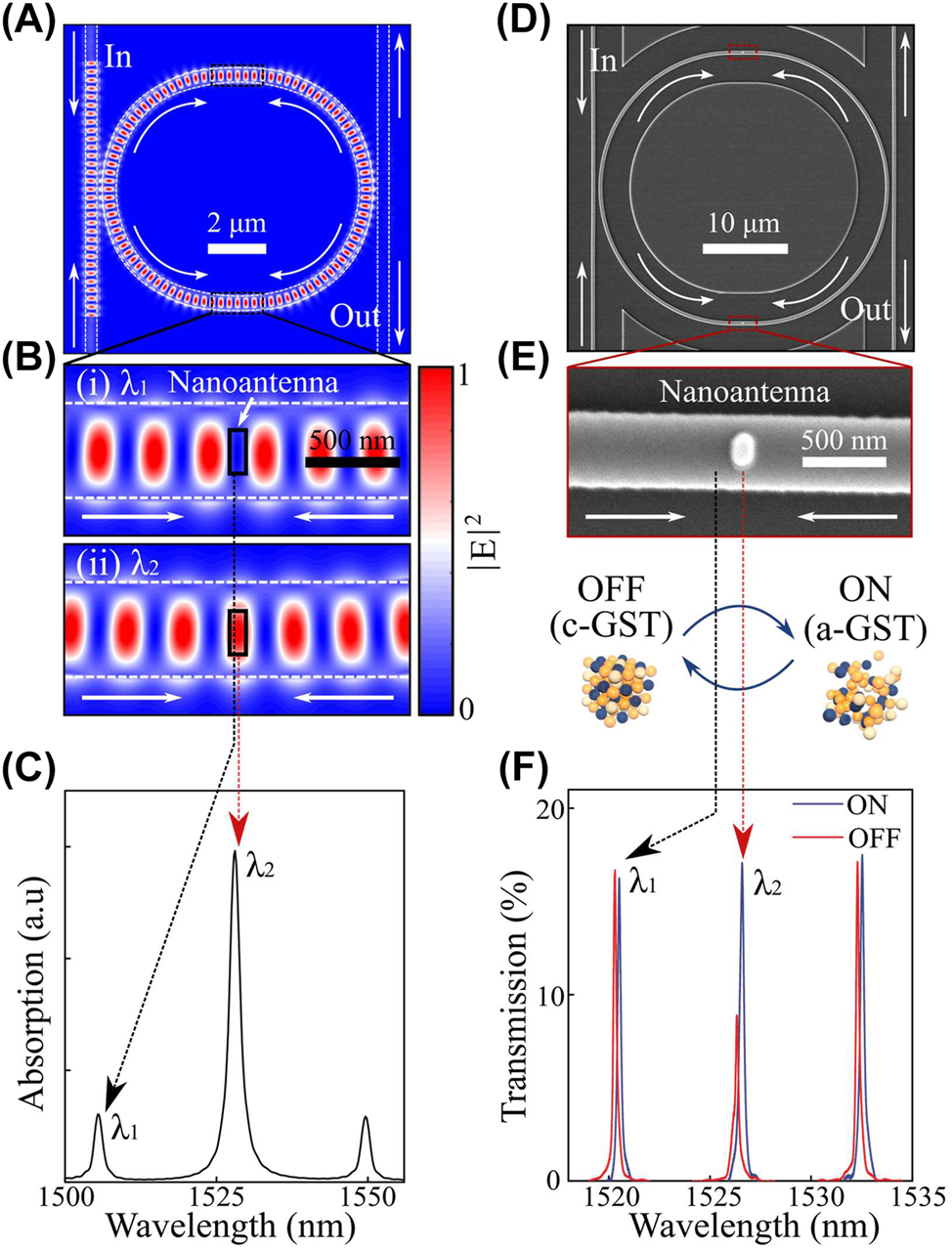
PSR in a microring resonator. (A and B) Electric-field distribution of a racetrack microring resonator when the counter-propagating waves from two input arms generate standing waves. Standing waves are out-of-phase depending on the incoming wavelength so that the active nanoantenna (i.e. GST) is invisible to the odd-mode (top, 1505 nm (λ 1)), but evanescently coupled to the even-mode (bottom, 1528 nm (λ 2)). Scale bars are 2 µm and 500 nm, respectively. (C) Absorption spectrum of the active nanoantenna that shows a selectively high absorption at the even-mode. (D and E) SEM scan of a racetrack microring resonator with active nanoantenna deposited on a waveguide. Scale bars are 10 µm and 500 nm, respectively. (F) Transmission spectra of a racetrack mirroring resonator when the nanoantenna is in (blue, ON) as-deposited amorphous and (red, OFF) crystalline phase after heating the device onto a hot-plate.
We then proceed to demonstrate the concept of PSR experimentally. Figure 2D and E shows a scanning electron micrograph (SEM) of the fabricated devices (Detailed parameters are described in Methods and Supplementary Figure 3). The active GST/SiO2 nanoantenna of 100 nm width, 250 nm length and a combined thickness of 30 nm (25 nm GST at the bottom with 5 nm SiO2 on the top) is located at each arm of the microring to increase the interaction strength with standing waves. Two counter propagating waves in a microring-resonator generate standing waves and eventually outcouple to drop waveguides where the output transmission is monitored (see Methods and Supplementary Figure 4). The mode overlap between oscillating electric-field and nanoantennas leads propagating light to be attenuated by the insertion loss of nanoantennas in a wavelength-selective manner, where the insertion loss is tunable in our case upon the crystallization of GST. The optical transmission levels of selected modes are modulated by phase-change of the GST. Figure 2F shows the experimentally measured selective reduction of even-mode transmission (λ
2) when the GST is switched from the as-deposited amorphous state to the lossy crystalline state after heating it onto a hot-plate at 200 °C for 5 min. The even-mode resonance (λ
2) exhibits attenuation by 49.2 % while odd-mode (λ
1) is unaffected (
We then investigate the capability to actively reconfigure the active nanoantennas using optical write pulses. Here, we exploit wavelength itself as a tunable factor to reconfigure the device states. Because the crystalline state of the GST is fully reversible [27], we can start a set of switching experiments from any states. For the experiments in Figure 3, amorphous phase is the initial state and we use GST/Au heterostructures on the partially-etched waveguide to enhance the absorptive coupling [17], [18], [34] (see Methods and Section S2). Since the nanoantennas are located at the spatial location of even-mode resonances (λ
2), we illuminate the set (220 pJ for 10 ns followed by 1.8 nJ for 300 ns with repetition of 50 times at intervals of 10 µs) and the reset (220 pJ for 10 ns) pulses selectively at the even-mode wavelength (1533.5 nm) to achieve fully reversible switching. Since the exact spectral position of the microring resonances differs between devices due to our device fabrication tolerances (Section S1), a different pair of odd- and even-mode wavelengths is selected for each microring device. For set (crystallization) processes, double-step pulses are used to enhance the reliability of its reversible switching [35]. As a result, the reversible states are only observed in the even-mode wavelength (λ
2, 1539.5 nm) while the odd-mode (λ
1, 1533.5 nm) is unaffected (Figure 3A). The modulation contrast for the even-mode resonance remains around 10 %, whereas the one for the odd-mode is below 1.6 % (Figure 3B). When the laser pulses are sent to odd-mode resonances, the absence of a mode maximum induces negligible transmission contrast (
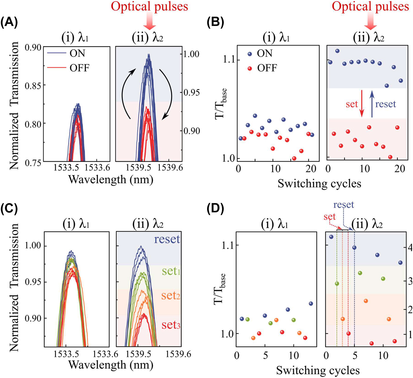
Wavelength-selectively reconfigurable system by optical pulses. (A) Enlarged transmission spectra of the PSR system with active nanoantennas (GST/Au) at the odd-mode (left, λ 1) and the even mode (right, λ 2), respectively. The set (220 pJ for 10 ns + 1.8 nJ for 300 ns with repetition of 50 times) and reset (220 pJ for 10 ns) optical pulses are sent to the device at the even-mode wavelength so that the reconfigurable transmission levels are only achieved in the even-mode wavelength. (B) Switching cyclability of wavelength-selective switching as in A. (C) Enlarged transmission spectra of multi-level wavelength-selective operations at the odd-mode (left, λ 1) and the even-mode (right, λ 2), respectively. The wavelength of optical pulses is at the even-mode and the number of such set pulses vary from 10 to 50. (D) Switching cyclability of wavelength-selective multi-level operations as in C.
The optical transmission levels are also dependent on the fractional volume of the switched crystalline domains in the GST. Therefore, by controlling the energy of input pulses, we can achieve the variation of intermediate transmission levels [9], [35], [39], [40]. We vary the number of set pulses [3] from 10 to 50 to achieve multi-level crystallization (Figure 3C and D). Upon the excitation of even-mode pulses (1539.5 nm), our device exhibit 4 distinct multi-levels selectively at the even-mode wavelength, but not at the odd-mode wavelength (1533.5 nm). Such programmable multi-level operation is repeatable for multiple cycles. This is a significant improvement over a standard microring resonator which exhibits non-selective tunability at every wavelength.
We further extend the model of PSR to realize a reconfigurable and multi-spectral optical filter, with intensity independently controlled at each wavelength. As shown in Figure 4A, two sets of GST/Au nanoantennas are placed on a racetrack ring resonator with spacing of 460 nm (3λ/4n eff), such that they are positioned at each node of two photonic modes (i.e. odd- and even-modes). The mode-selective coupling induces wavelength-selective accessibility to individual nanoantennas, and therefore the intensities of wavelength-selective input (P λ1 and P λ2) are independently modulated by the wavelength-selective weighting coefficients (G left and G right). Figure 4B and C shows that left and right nanoantennas exhibit selective absorptive coupling at odd-and even-mode resonances, respectively, resulting in the absorption contrast at each resonant wavelength. Such absorption contrast is used to set the threshold of selective switching for individual naonantennas. We experimentally verify this by showing the wavelength-selective multi-level operation (Figure 4D and E) and switching cyclability (Supplementary Figure 8) at each photonic mode. Upon odd-mode (λ 1, 1530.3 nm) illumination, we note that the laser power is sufficient to selectively switch the left nanoantenna, but not sufficient to switch the right nanoantenna. Therefore, independent multi-level encoding can be demonstrated selectively (left nanoantenna, Figure 4D). In this case, we start in the crystalline state and control the reset pulse duration [35] from 10 ns to 25 ns to vary the fractional volume of the amorphized GST. By sending these pulses at the odd-mode resonance, five multi-levels are wavelength-selectively encoded without affecting the even-mode. This process is fully reversible as these multi-levels can be erased back to the initial state by high-power set pulse. The thermo-optic delay time [41] is neglected and this is a reasonable approximation, owing to the confined volume of GST nanoantennas on a thermally-conductive silicon waveguide [42]. Such wavelength-selectivity is also reproduced with reversed mode selections under even-mode illumination (λ 2, 1536. 5 nm) as demonstrated in Figure 4E.
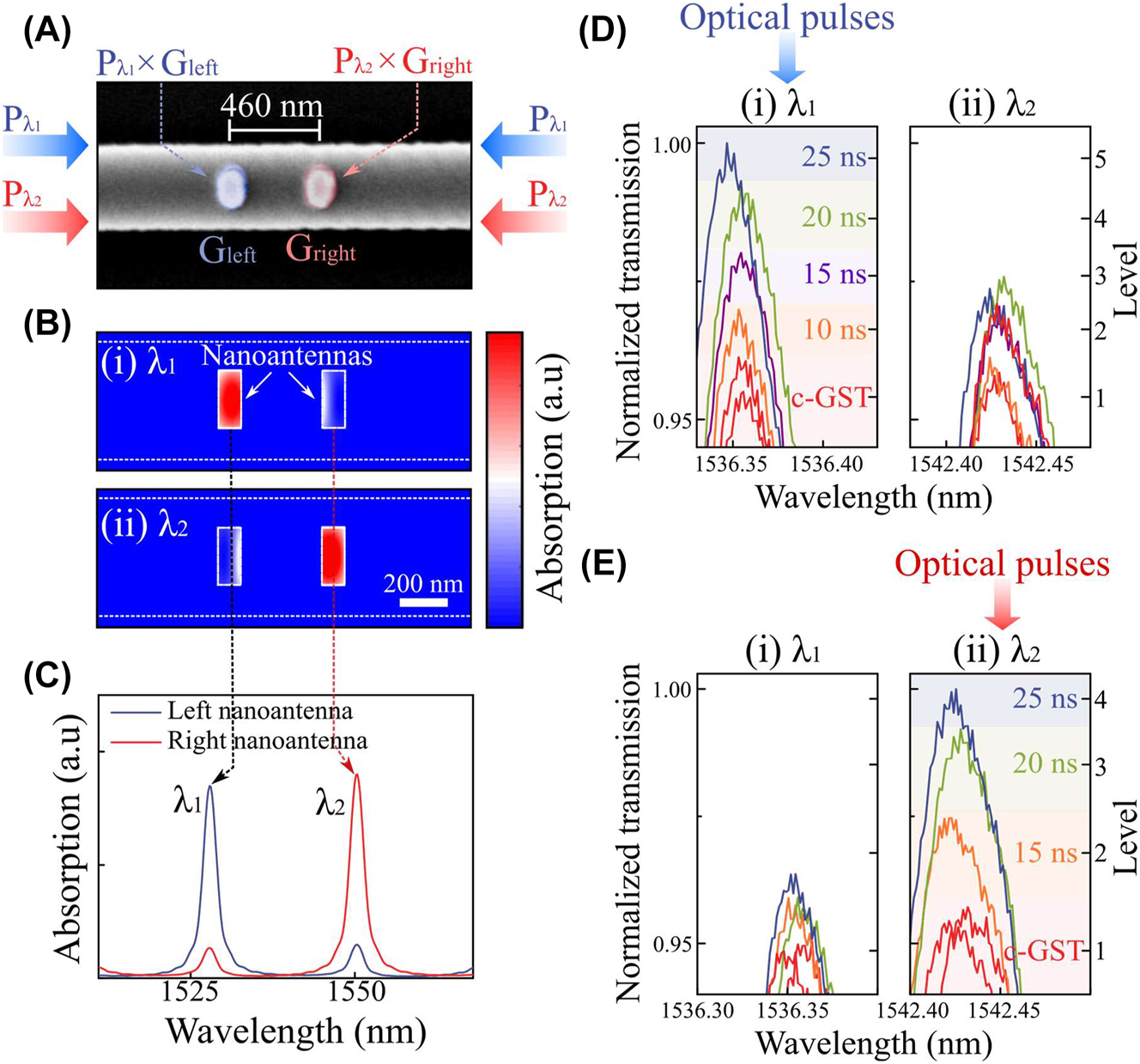
Reconfigurable multi-spectral filter in a single element. (A) Colorized SEM image of an enlarged view of the active nanoantennas (GST/Au) on a waveguide for PSR system. The separation between two nanoantennas is 460 nm. Wavelength-selective input signals (P λ1 and P λ2) are independently modulated by weighting coefficients of each nanoantenna (G left and G right). (B) Absorption profile of the PSR system with double nanoantennas, where the odd-mode (top, 1528 nm (λ 1)) couples with the left nanoantenna and the even-mode (bottom, 1550 nm (λ 2)) couples with the right nanoantenna. (C) Absorption spectra at each nanoantenna showing the wavelength-selective absorption contrast. (D and E) Enlarged transmission spectra of intensity-tunable multi-spectral filter at the odd-mode (left, 1536 nm (λ 1)) and the even-mode (right, 1542 nm (λ 2)), respectively. Reset pulses of 220 pJ (10 ns) with varying the pulse duration from 10 to 25 ns are used to provide wavelength-selective multi-levels under (D) odd-mode and (E) even-mode illumination. The piecewise set pulse of (220 pJ for 10 ns + 1.8 nJ for 300 ns with repetition of 50 times) is used for initializing the transmission level.
Thus, our reconfigurable multi-spectral filter provides independent accessibility to each nanoantenna with decoupled parameters. For example, our multi-spectral modulator can be utilized with a broadband light source such as supercontinuum laser [33] or optical frequency comb [43]. It is worth nothing that this approach is all-optical and non-volatile, providing a significant advantage over electro-optic or thermo-optical components (described in Section S3). Importantly, this functionality is achieved in a single on-chip photonic unit, instead of using multiple ring resonators [9] or free-space optical illumination [17]. Therefore, we demonstrate a compact building block of wavelength-selective photonic interconnects that can be exploited as reconfigurable optical filters [44], wavelength-division multiplexing/demultiplexing [45] or in-memory computing units [40]. Furthermore, such building block can achieve a dramatic enhancement of overall optical storage capacity as it gets upscaled, for instance by assembling multiple ring resonators in series (Supplementary Figure 15) or coupled to each other and tailoring their ring sizes (i.e. FSR). In this case, the precise control spatio-spectral overlap is essential which can be achieved by tuning the relative optical phases of two input light (Supplementary Figures 9–11). Phase shifters can be implemented outside a microring resonator by using thermo- or electro-optical modulators that enhance the robustness of system and provide extra degrees-of-freedom in phase domain.
Also, the concept of PSR is readily generalized to other photonic components such as plain waveguides or multimode interferometers (MMI) while the spectral selectivity is determined by the spatial location of active material along the propagation axis (Supplementary Figure 12). This spatio-spectral relation raises interesting possibilities for the exploitation of more than two wavelength-selective channels in a single microring resonator (Section S4.2). Although a tradeoff exists between device footprint and number of modulations, three independent modulations with the crosstalk of <−15 dB can feasibly be implemented (Supplementary Figure 13); this can be further improved by optimizing the geometrical or material properties of nanoantennas [38], [46], [47] (described in Section S2). However, as the number of modulation increases, the high-precision post-processing techniques [48] will be required to fine-tune the spectral resonance positions of microring resonators, compensating for its low fabrication tolerance. Because our PSR system allows for (de)multiplexing functionalities at highly confined scales, the overall modulation or multiplexing densities are found to be several orders of magnitude higher than those of other integrated multiplexing switches [49], [50], [51], [52] (described in Section S4.3). This wavelength-selective reconfigurability at sub-microns scale offers a promising avenue for programmable and compact photonic networks that can exploit large bandwidths or for sensing or imaging applications that require high-resolution spectral or spatial information.
3 Conclusions
In summary, we demonstrate a compact prototype of an integrated, wavelength-selective, reconfigurable device in which the intensity of light can be independently modulated at each wavelength channel of a single photonic element. Our approach exploits the concept of coherent perfect absorption with non-volatile tunability of phase-change material, thereby enabling the use of spatial degrees-of-freedom in integrated photonics and the realization of ultracompact reconfigurability, or PSR. Our device exhibits excellent spatial and spectral resolution by combining the WGM resonances in a microring resonator with active phase-change nanoantennas. The strong optical confinement of the electric-field within our nanoantennas allows for maintaining wavelength-addressability at highly confined spatial scales. Using this approach, we demonstrate a photonic, reconfigurable, multi-spectral filter at the single element level. Our results provide the groundwork for realizing functional photonic circuits having input wavelengths as variables and can serve as the building block of wavelength-multiplexed coherent nanophotonics, opening up a myriad of potential applications in neuromorphic networks, in-memory computing paradigms, optical communications, or high-resolution imaging applications.
4 Methods
4.1 Device fabrication
A first run of electron-beam lithography (EBL) was performed on a 220 nm Si on 3 µm oxide layer to fabricate waveguides, grating couplers, multimode-interferometers (MMIs) and microring resonators with using positive tone resist (CSAR62). After development, the patterned substrate was etched at a depth of 110 nm by reactive-ion etching (RIE, Oxford Instruments) with a gas mixture of CHF3/Ar/O2. A second EBL was carried out with double-layered PMMA resist to define the nanoantennas with widths of 100 nm and lengths of 250 nm on microring resonators. After development, the patterned substrate was subjected to a lift-off process followed by RIE at a depth of 30 nm and RF-sputtering (Nordiko) of GST/SiO2 of 25 and 5 nm thickness, respectively. For active switching experiments (Figures 3 and 4), additional Cr/Au layers of 3 and 20 nm thickness, respectively, were deposited in advance of a lift-off process to enhance the absorption of nanoantennas. We finely swept the positions of nanoantennas onto an array of microring resonators so that optimal spatio-spectral overlap can be obtained (Supplementary Figure 11). Also, in advance of active switching, the fabricated devices were heated on a hot-plate (200 °C) for 5 min to fully crystallize the GST.
4.2 Measurement setup
The measurement was carried out using the setup described in Supplementary Figure 4. A tunable laser (Santec, TSL-550) was used to optically probe the device at telecommunication range (1500–1600 nm), while the input and output grating couplers were optimized at 1550 nm wavelength. The coupled light was separated by MMIs at a ratio of 50:50 and recombined into a microring resonator. Optical transmission and spectral responses of drop waveguides were measured from output grating couplers using a 200-kHz low-noise photoreceiver (New Focus, Model 2011). For optical programming, the pump line was separated by optical splitter (90:10), which was modulated by an electro-optical modulator (EOM, Lucent Technologies) with an electrical pulse generator (AFG3102C, Tektronix). The generated optical pulses were amplified by an erbium-doped fiber amplifier (EDFA, HPP-PMFA-21-10 from Pritel) and monitored by a 125-MHz low-noise photoreceiver (New Focus, 1811) with an oscilloscope (Telktronix, TDS7404B). Rack optical switch (Gezhi) and circulator were used to separate the probe transmission from pump line for spectral measurement. Double-step pulses were used for a crystallization process which can produce more repeatable phase-change transition [35]. The number of pulses [3] was controlled for multi-level crystallization (Figure 3) and the pulse duration [35] was modulated for multi-level amorphization (Figure 4). Different microring devices were used for a single nanoantenna measurement in Figure 2F and 3. All of measurement with modulation of pulses was carried out by a custom-built program (Labview).
Funding source: EPSRC
Funding source: EU
Award Identifier / Grant number: FunComp
Award Identifier / Grant number: Phoenics
Acknowledgments
The authors acknowledge discussions with A.Ne.
-
Research funding: The authors acknowledge partial support via funding from the EU H2020 programme (Grant No. 780848, Fun-COMP Project) and (Grant No. 101017237, PHOENICS Project). This research was funded in part by the UKRI [EP/T023899/1, EP/R001677/1 and EP/W022931/1].
-
Author contributions: JSL, NF and HB conceived the concept. JSL and NF carried out the fabrication, simulation and measurements. All authors provided in-depth discussions and suggestions at all stages of the work, discussed the results and wrote the manuscript, with HB leading the work.
-
Conflict of interest: Authors state no conflicts of interest.
-
Data availability: All data needed to evaluate the conclusion in the paper are present in the paper and/or the Supplementary Information.
References
[1] W. Bogaerts, et al.., “Programmable photonic circuits,” Nature, vol. 586, pp. 207–216, 2020. https://doi.org/10.1038/s41586-020-2764-0.Suche in Google Scholar PubMed
[2] J. Feldmann, et al.., “Parallel convolutional processing using an integrated photonic tensor core,” Nature, vol. 589, pp. 52–58, 2021. https://doi.org/10.1038/s41586-020-03070-1.Suche in Google Scholar PubMed
[3] Z. Cheng, C. Ríos, H. P. Pernice Wolfram, C. D. Wright, and H. Bhaskaran, “On-chip photonic synapse,” Sci. Adv., vol. 3, no. 9, p. e1700160, 2017. https://doi.org/10.1126/sciadv.1700160.Suche in Google Scholar PubMed PubMed Central
[4] H. T. Peng, M. A. Nahmias, T. F. d. Lima, A. N. Tait, and B. J. Shastri, “Neuromorphic photonic integrated circuits,” IEEE J. Sel. Top. Quantum Electron., vol. 24, no. 6, pp. 1–15, 2018. https://doi.org/10.1109/jstqe.2018.2840448.Suche in Google Scholar
[5] A. N. Tait, et al.., “Neuromorphic photonic networks using silicon photonic weight banks,” Sci. Rep., vol. 7, p. 7430, 2017. https://doi.org/10.1038/s41598-017-07754-z.Suche in Google Scholar PubMed PubMed Central
[6] X. Guo, J. Xiang, Y. Zhang, and Y. Su, “Integrated neuromorphic photonics: synapses, neurons, and neural networks,” Adv. Photonics Res., vol. 2, no. 6, p. 2000212, 2021. https://doi.org/10.1002/adpr.202000212.Suche in Google Scholar
[7] S. Aggarwal, B. Dong, J. Feldmann, N. Farmakidis, W. H. P. Pernice, and H. Bhaskaran, “Reduced rank photonic computing accelerator,” Optica, vol. 10, no. 8, pp. 1074–1080, 2023. https://doi.org/10.1364/optica.485883.Suche in Google Scholar
[8] S. Schuler, et al.., “High-responsivity graphene photodetectors integrated on silicon microring resonators,” Nat. Commun., vol. 12, p. 3733, 2021. https://doi.org/10.1038/s41467-021-23436-x.Suche in Google Scholar PubMed PubMed Central
[9] C. Ríos, et al.., “Integrated all-photonic non-volatile multi-level memory,” Nat. Photonics, vol. 9, pp. 725–732, 2015. https://doi.org/10.1038/nphoton.2015.182.Suche in Google Scholar
[10] Y. Zhang, et al.., “Broadband transparent optical phase change materials for high-performance nonvolatile photonics,” Nat. Commun., vol. 10, p. 4279, 2019. https://doi.org/10.1038/s41467-019-12196-4.Suche in Google Scholar PubMed PubMed Central
[11] H. Zhou, et al.., “Photonic matrix multiplication lights up photonic accelerator and beyond,” Light: Sci. Appl., vol. 11, p. 30, 2022. https://doi.org/10.1038/s41377-022-00717-8.Suche in Google Scholar PubMed PubMed Central
[12] N. C. Harris, et al.., “Efficient, compact and low loss thermo-optic phase shifter in silicon,” Opt. Express, vol. 22, no. 9, pp. 10487–10493, 2014. https://doi.org/10.1364/oe.22.010487.Suche in Google Scholar PubMed
[13] K. Powell, et al.., “Integrated silicon carbide electro-optic modulator,” Nat. Commun., vol. 13, p. 1851, 2022. https://doi.org/10.1038/s41467-022-29448-5.Suche in Google Scholar PubMed PubMed Central
[14] M. Li, J. Ling, Y. He, U. A. Javid, S. Xue, and Q. Lin, “Lithium niobate photonic-crystal electro-optic modulator,” Nat. Commun., vol. 11, p. 4123, 2020. https://doi.org/10.1038/s41467-020-17950-7.Suche in Google Scholar PubMed PubMed Central
[15] L. Midolo, A. Schliesser, and A. Fiore, “Nano-opto-electro-mechanical systems,” Nat. Nanotechnol., vol. 13, pp. 11–18, 2018. https://doi.org/10.1038/s41565-017-0039-1.Suche in Google Scholar PubMed
[16] D. G. Baranov, A. Krasnok, T. Shegai, A. Alù, and Y. Chong, “Coherent perfect absorbers: linear control of light with light,” Nat. Rev. Mater., vol. 2, p. 17064, 2017. https://doi.org/10.1038/natrevmats.2017.64.Suche in Google Scholar
[17] B. Chen, et al.., “Hybrid photon–plasmon coupling and ultrafast control of nanoantennas on a silicon photonic chip,” Nano Lett., vol. 18, no. 1, pp. 610–617, 2018. https://doi.org/10.1021/acs.nanolett.7b04861.Suche in Google Scholar PubMed
[18] L. Jiang, et al.., “In-plane coherent control of plasmon resonances for plasmonic switching and encoding,” Light: Sci. Appl., vol. 8, p. 21, 2019. https://doi.org/10.1038/s41377-019-0134-1.Suche in Google Scholar PubMed PubMed Central
[19] W. Wan, Y. Chong, L. Ge, H. Noh, A. D. Stone, and H. Cao, “Time-reversed lasing and interferometric control of absorption,” Science, vol. 331, no. 6019, pp. 889–892, 2011. https://doi.org/10.1126/science.1200735.Suche in Google Scholar PubMed
[20] L. Feng, J. Wong Zi, R.-M. Ma, Y. Wang, and X. Zhang, “Single-mode laser by parity-time symmetry breaking,” Science, vol. 346, no. 6212, pp. 972–975, 2014. https://doi.org/10.1126/science.1258479.Suche in Google Scholar PubMed
[21] M. Papaioannou, E. Plum, J. Valente, E. T. F. Rogers, and N. I. Zheludev, “Two-dimensional control of light with light on metasurfaces,” Light: Sci. Appl., vol. 5, pp. e16070, 2016. https://doi.org/10.1038/lsa.2016.70.Suche in Google Scholar PubMed PubMed Central
[22] X. Fang, K. F. MacDonald, and N. I. Zheludev, “Controlling light with light using coherent metadevices: all-optical transistor, summator and invertor,” Light: Sci. Appl., vol. 4, pp. e292, 2015. https://doi.org/10.1038/lsa.2015.65.Suche in Google Scholar
[23] M. Wuttig and N. Yamada, “Phase-change materials for rewriteable data storage,” Nat. Mater., vol. 6, pp. 824–832, 2007. https://doi.org/10.1038/nmat2009.Suche in Google Scholar PubMed
[24] Z. Cheng, et al.., “Antimony thin films demonstrate programmable optical nonlinearity,” Sci. Adv., vol. 7, no. 1, p. eabd7097, 2021. https://doi.org/10.1126/sciadv.abd7097.Suche in Google Scholar PubMed PubMed Central
[25] J. S. Lee, N. Farmakidis, C. D. Wright, and H. Bhaskaran, “Polarization-selective reconfigurability in hybridized-active-dielectric nanowires,” Sci. Adv., vol. 8, no. 24, p. eabn9459, 2022. https://doi.org/10.1126/sciadv.abn9459.Suche in Google Scholar PubMed PubMed Central
[26] R. Alaee, M. Albooyeh, S. Tretyakov, and C. Rockstuhl, “Phase-change material-based nanoantennas with tunable radiation patterns,” Opt. Lett., vol. 41, no. 17, pp. 4099–4102, 2016. https://doi.org/10.1364/ol.41.004099.Suche in Google Scholar PubMed
[27] S. Raoux, F. Xiong, M. Wuttig, and E. Pop, “Phase change materials and phase change memory,” MRS Bull., vol. 39, pp. 703–710, 2014. https://doi.org/10.1557/mrs.2014.139.Suche in Google Scholar
[28] N. Farmakidis, et al.., “Plasmonic nanogap enhanced phase-change devices with dual electrical-optical functionality,” Sci. Adv., vol. 5, no. 11, p. eaaw2687, 2019. https://doi.org/10.1126/sciadv.aaw2687.Suche in Google Scholar PubMed PubMed Central
[29] S. Song, J. Dua, and C. B. Arnold, “Influence of annealing conditions on the optical and structural properties of spin-coated As2S3 chalcogenide glass thin films,” Opt. Express, vol. 18, no. 6, pp. 5472–5480, 2010. https://doi.org/10.1364/oe.18.005472.Suche in Google Scholar
[30] H. Jayatilleka, et al.., “Post-fabrication trimming of silicon photonic ring resonators at wafer-scale,” J. Lightwave Technol., vol. 39, no. 15, pp. 5083–5088, 2021. https://doi.org/10.1109/jlt.2021.3079801.Suche in Google Scholar
[31] Y. Wu, H. Shang, X. Zheng, and T. Chu, “Post-processing trimming of silicon photonic devices using femtosecond laser,” Nanomaterials, vol. 13, no. 6, p. 1031, 2023. https://doi.org/10.3390/nano13061031.Suche in Google Scholar PubMed PubMed Central
[32] V. Biryukova, G. J. Sharp, C. Klitis, and M. Sorel, “Trimming of silicon-on-insulator ring-resonators via localized laser annealing,” Opt. Express, vol. 28, no. 8, pp. 11156–11164, 2020. https://doi.org/10.1364/oe.389948.Suche in Google Scholar
[33] B. Dong, et al.., “Higher-dimensional processing using a photonic tensor core with continuous-time data,” Nat. Photonics, vol. 17, pp. 1080–1088, 2023. https://doi.org/10.1038/s41566-023-01313-x.Suche in Google Scholar
[34] R. Ritter, et al.., “Coupling thermal atomic vapor to slot waveguides,” Phys. Rev. X, vol. 8, no. 2, p. 021032, 2018. https://doi.org/10.1103/physrevx.8.021032.Suche in Google Scholar
[35] X. Li, et al.., “Fast and reliable storage using a 5 bit, nonvolatile photonic memory cell,” Optica, vol. 6, no. 1, pp. 1–6, 2019. https://doi.org/10.1364/optica.6.000001.Suche in Google Scholar
[36] J. Feldmann, et al.., “Calculating with light using a chip-scale all-optical abacus,” Nat. Commun., vol. 8, p. 1256, 2017. https://doi.org/10.1038/s41467-017-01506-3.Suche in Google Scholar PubMed PubMed Central
[37] P. Xu, J. Zheng, J. K. Doylend, and A. Majumdar, “Low-loss and broadband nonvolatile phase-change directional coupler switches,” ACS Photonics, vol. 6, no. 2, pp. 553–557, 2019. https://doi.org/10.1021/acsphotonics.8b01628.Suche in Google Scholar
[38] C. Ríos, et al.., “Ultra-compact nonvolatile phase shifter based on electrically reprogrammable transparent phase change materials,” PhotoniX, vol. 3, p. 26, 2022. https://doi.org/10.1186/s43074-022-00070-4.Suche in Google Scholar
[39] C. Rios, et al.., “Controlled switching of phase-change materials by evanescent-field coupling in integrated photonics [Invited],” Opt. Mater. Express, vol. 8, no. 9, pp. 2455–2470, 2018. https://doi.org/10.1364/ome.8.002455.Suche in Google Scholar
[40] C. Ríos, et al.., “In-memory computing on a photonic platform,” Sci. Adv., vol. 5, no. 2, p. eaau5759, 2019. https://doi.org/10.1126/sciadv.aau5759.Suche in Google Scholar PubMed PubMed Central
[41] M. Stegmaier, C. Ríos, H. Bhaskaran, and W. H. P. Pernice, “Thermo-optical effect in phase-change nanophotonics,” ACS Photonics, vol. 3, no. 5, pp. 828–835, 2016. https://doi.org/10.1021/acsphotonics.6b00032.Suche in Google Scholar
[42] X. Li, et al.., “Experimental investigation of silicon and silicon nitride platforms for phase-change photonic in-memory computing,” Optica, vol. 7, no. 3, pp. 218–225, 2020. https://doi.org/10.1364/optica.379228.Suche in Google Scholar
[43] T. Herr, et al.., “Temporal solitons in optical microresonators,” Nat. Photonics, vol. 8, pp. 145–152, 2014. https://doi.org/10.1038/nphoton.2013.343.Suche in Google Scholar
[44] W. Liu, et al.., “A fully reconfigurable photonic integrated signal processor,” Nat. Photonics, vol. 10, pp. 190–195, 2016. https://doi.org/10.1038/nphoton.2015.281.Suche in Google Scholar
[45] P. Dong, “Silicon photonic integrated circuits for wavelength-division multiplexing applications,” IEEE J. Sel. Top. Quantum Electron., vol. 22, pp. 370–378, 2016. https://doi.org/10.1109/jstqe.2016.2575358.Suche in Google Scholar
[46] Z. Fang, J. Zheng, A. Saxena, J. Whitehead, Y. Chen, and A. Majumdar, “Non-volatile reconfigurable integrated photonics enabled by broadband low-loss phase change material,” Adv. Opt. Mater., vol. 9, p. 2002049, 2021. https://doi.org/10.1002/adom.202002049.Suche in Google Scholar
[47] A. G. Kusne, et al.., “On-the-fly closed-loop materials discovery via Bayesian active learning,” Nat. Commun., vol. 11, p. 5966, 2020. https://doi.org/10.1038/s41467-020-19597-w.Suche in Google Scholar PubMed PubMed Central
[48] N. Farmakidis, et al.., “Scalable high-precision trimming of photonic resonances by polymer exposure to energetic beams,” Nano Lett., vol. 23, no. 11, pp. 4800–4806, 2023. https://doi.org/10.1021/acs.nanolett.3c00220.Suche in Google Scholar PubMed PubMed Central
[49] H. Jia, L. Zhang, J. Ding, L. Zheng, C. Yuan, and L. Yang, “Microring modulator matrix integrated with mode multiplexer and de-multiplexer for on-chip optical interconnect,” Opt. Express, vol. 25, no. 1, pp. 422–430, 2017. https://doi.org/10.1364/oe.25.000422.Suche in Google Scholar
[50] H. Jayatilleka, K. Murray, M. Caverley, N. A. F. Jaeger, L. Chrostowski, and S. Shekhar, “Crosstalk in SOI microring resonator-based filters,” J. Lightwave Technol., vol. 34, no. 12, pp. 2886–2896, 2016. https://doi.org/10.1109/jlt.2015.2480101.Suche in Google Scholar
[51] L.-W. Luo, et al.., “WDM-compatible mode-division multiplexing on a silicon chip,” Nat. Commun., vol. 5, p. 3069, 2014. https://doi.org/10.1038/ncomms4069.Suche in Google Scholar PubMed
[52] H. Xu, C. Liu, D. Dai, and Y. Shi, “Direct-access mode-division multiplexing switch for scalable on-chip multi-mode networks,” Nanophotonics, vol. 10, no. 18, pp. 4551–4566, 2021. https://doi.org/10.1515/nanoph-2021-0441.Suche in Google Scholar
Supplementary Material
This article contains supplementary material (https://doi.org/10.1515/nanoph-2023-0651).
© 2023 the author(s), published by De Gruyter, Berlin/Boston
This work is licensed under the Creative Commons Attribution 4.0 International License.
Artikel in diesem Heft
- Frontmatter
- Editorial
- Programmable nano-optics and photonics
- Reviews
- Towards large-scale programmable silicon photonic chip for signal processing
- Phase change material-based tunable Fano resonant optical coatings and their applications
- Perspectives
- Melting-free integrated photonic memory with layered polymorphs
- Chalcogenide phase-change material advances programmable terahertz metamaterials: a non-volatile perspective for reconfigurable intelligent surfaces
- Research Articles
- Fundamental limits to multi-functional and tunable nanophotonic response
- Spatio-spectral control of coherent nanophotonics
- Nanoantenna induced liquid crystal alignment for high performance tunable metasurface
- Programmable topological metasurface to modulate spatial and surface waves in real time
- Programmable flip-metasurface with dynamically tunable reflection and broadband undistorted transmission
- High-resolution non-line-of-sight imaging based on liquid crystal planar optical elements
- Ultrafast Q-boosting in semiconductor metasurfaces
- Inverse design of compact nonvolatile reconfigurable silicon photonic devices with phase-change materials
- Integrated multi-operand optical neurons for scalable and hardware-efficient deep learning
- Surface plasmon-cavity hybrid state and its graphene modulation at THz frequencies
- Language-controllable programmable metasurface empowered by large language models
- All optical tunable RF filter using elemental antimony
- Reconfigurable application-specific photonic integrated circuit for solving partial differential equations
- Optimization of a programmable λ/2-pitch optical phased array
- Closed-loop electron-beam-induced spectroscopy and nanofabrication around individual quantum emitters
- High-fidelity and polarization-insensitive universal photonic processors fabricated by femtosecond laser writing
- Direct electron beam patterning of electro-optically active PEDOT:PSS