Reconfigurable nonlinear optical element using tunable couplers and inverse-designed structure
-
Vahid Nikkhah
 ,
Mario Junior Mencagli
and
Nader Engheta
,
Mario Junior Mencagli
and
Nader Engheta


Abstract
In recent years, wave-based analog computing has been at the center of attention for providing ultra-fast and power-efficient signal processing enabled by wave propagation through artificially engineered structures. Building on these structures, various proposals have been put forward for performing computations with waves. Most of these proposals have been aimed at linear operations, such as vector-matrix multiplications. The weak and hardly controllable nonlinear response of electromagnetic materials imposes challenges in the design of wave-based structures for performing nonlinear operations. In the present work, first, by using the method of inverse design we propose a three-port device, which consists of a combination of linear and Kerr nonlinear materials, exhibiting the desired power-dependent transmission properties. Then, combining a proper arrangement of such devices with a collection of Mach–Zehnder interferometers (MZIs), we propose a reconfigurable nonlinear optical architecture capable of implementing a variety of nonlinear functions of the input signal. The proposed device may pave the way for wave-based reconfigurable nonlinear signal processing that can be combined with linear networks for full-fledged wave-based analog computing.
1 Introduction
Optical nonlinearity plays a crucial role in several exciting areas of research [1–4]. Among these areas, emerging optical neural networks (ONNs) [5, 6] which are a physical implementation of a standard artificial neural network (ANN) with optical components, have received growing interest. ONNs have several advantages over their electronic counterparts. Among these advantages, it is worth emphasizing their higher computational speed with lower power consumption. These features make them appealing for several applications that require handling large data sets such as real-time image processing [7], language translation [8], decision-making problems [9], and more [10, 11]. One of the most important units in the ANN structure is the activation function [12]. This function determines the neural network output, its accuracy, and the computational efficiency of a training model. Activation functions can be described by simple mathematical nonlinear functions. In recent years, different nonlinear functions, acting as activation functions, have been investigated in the ANN community. It turned out that the nonlinear activation function’s choice is closely connected with the ANN application [12]. Diverse ANN applications require the use of different nonlinear activation functions. For example, the sigmoid function, which is the most common nonlinear activation function, is particularly suitable for applications that produce output values in the range of [0,1]. Despite the mathematical simplicity of nonlinear activation functions, it is still unclear how to perform arbitrary nonlinear functions on waves physically or even in principle whether such functions are generally possible. Current nonlinear optical components, such as bistable and saturable absorber devices [5, 6, 13], can implement only a subset of all the possible nonlinear activation functions. Moreover, most of them suffer from a lack of reconfigurability, which means that once they have been realized, the form of their nonlinear response cannot be changed. As a result, they can only be used to implement a single activation function limiting the ONN application range. In the present work, we introduce an idea for a reconfigurable architecture that can implement arbitrary nonlinear functions (within certain constraints) between the input signal, and the output signal (see Figure 1). The proposed architecture is composed of two networks: (1) the nonlinear signal divider and (2) the linear optical network composed of a mesh of Mach–Zehnder Interferometers (MZIs). The nonlinear optical network consists of a set of identical three-port devices functioning as specialized optical power limiters. These limiters employ a Kerr nonlinear material and a linear dielectric for limiting the optical signal/intensity of the light that is coupled to one of the output ports and the rest of the energy is coupled to another output port. The specific composition and spatial distributions of the Kerr material and the linear dielectric are obtained through the method of the inverse design [14– 19]. This method has opened up enormous opportunities both in linear and nonlinear optics for designing non-intuitive optical devices with complex functionalities. The optically-linear MZI portion of the proposed device consists of a properly arranged collection of MZIs, as shown in Figure 1. Photonic MZI meshes, which commonly consist of waveguide-based MZI array laid out on a flat silicon substrate, have attracted a great deal of attention in recent years [13, 20–25]. This interest mostly focuses on MZI networks that can be programmed to implement any linear transformations with electromagnetic waves [26–28]. Since such networks exploit the well-known computational capabilities of electromagnetic waves and are suitable for on-chip integration, it is playing an important role in several applications, including optical machine learning [5], quantum-information processing [25], forward scattering problems [29], and optical analog equation solving platform [30, 31]. Our proposed device here, thanks to its versatility and reconfigurability, may be useful for various applications in nonlinear photonics, such as ONNs mentioned above, in which reconfigurable nonlinear optical elements are needed.

General reconfigurable optical architecture for generating tunable nonlinear functions. The architecture is composed of a nonlinear and a linear network. The nonlinear network (yellowish-filled rectangular box) consists of a set of identical nonlinear three-port devices, each of which acts as a nonlinear power limiter. The linear network (bluish-filled rectangular box) consists of a collection of linear MZIs. The inset sketches a generic MZI mesh configuration.
Throughout the paper, we assume ejωt as the time dependence of EM fields.
2 Inverse-designed nonlinear power limiter for the nonlinear network
In this section, the required characteristics and design of the constitutive element of the nonlinear network, i.e., the nonlinear power limiter is discussed. As schematically illustrated in Figure 2(a), the nonlinear element is a three-port device that is required to exhibit the following transmission features. When a monochromatic signal, which is injected into the input port (Port 1) carries a power below a certain value, denoted as P sat, this signal should appear at the designated output port on the right (Port 2). If the power of the input signal exceeds P sat, the power of the signal at Port 2 should stay at its ”saturated” value, P sat, and the spillover of the input signal should be directed to the other output port on the bottom (Port 3). As the power of the input signal increases beyond P sat, the power reaching Port 3 keeps increasing, while the one going to Port 2 remains constant and equal to P sat. Also, as will become clear shortly, it is required that the phases of the output signals at Ports 2 and 3 be the same (and, with an additional part discussed in the MZI section, to be the same as the phase of the input signal). To achieve these transmission characteristics, we consider a design region containing a distribution of Kerr nonlinear and linear dielectric materials connected to the input and output ports through slab waveguides as depicted in Figure 2(a). The cladding surrounding the structure is assumed to be air. Without loss of generality, we also assume the structure to be two-dimensional (2D) meaning it is infinitely extended in the out-of-plane direction (z axis). The materials of the structure are invariant along the out-of-plane coordinate (z) and, as a result, the distribution of the electromagnetic (EM) fields is computed only over the in-plane geometry (x–y plane). Our proposed approach here is general and the choice of materials depends on the frequency of operation. Here, as a nonlinear material, we used a realistic high-index Kerr material such as As2S3 (arsenic sulfide), which is modeled with the following intensity-dependent permittivity [32]:
where

Inverse-designed nonlinear photonic structure as power limiter. (a) A transverse-electric (TE)-polarized optical signal is the input to the waveguide denoted as Port 1. The power of the output signal at Port 2 follows the power of the input signal but is limited when the input power increases beyond P sat. The rest of the energy is then directed toward Port 3. The optimized distribution of the Kerr nonlinear material (As2S3) and the linear dielectric (Si3N4) are, respectively, shown by blue and yellow regions. (b) The blue and green solid curves, respectively, show the transmitted power of the signals at Port 2 and Port 3 of the proposed element in panel (a) versus the input power. The dashed curves are the corresponding desired transmission plots. The red solid curve illustrates the reflected power back to Port 1. The eight red circles are the target samples of the input power for which the cost function is defined for optimization. (c)–(f) The magnitude of the electric field distribution (left side of each panel) and the nonlinear refractive index shift inside the Kerr medium (right side of each panel) simulated for different input power values, P in = 0.01P sat, P sat, 2P sat, 4P sat. (g) The phases of the output signals at Port 2 (blue solid curve) and Port 3 (green solid curve) relative to the input phase.
So far, we have discussed the performance of the three-port inverse-designed nonlinear power limiter for a discrete number of input power values. In Figure 2(b), the solid blue and green lines, respectively, show the transmitted power from Port 1 to Ports 2 and 3 which are calculated by continuously sweeping the input power from 0 to 4P
sat. As observed from the transmission plots, The agreement with the target responses (dashed curves) is quite good. For P
in ≤ P
sat, the power reaching Port 2 increases linearly. For the input powers beyond P
sat, the output power at Port 2 saturates around P
sat and the power going to Port 3 starts increasing almost linearly with P
in. Figure 2(g) shows the relative phase variation between the output signals (Ports 2 and 3) and the input signal (Port 1) versus the input power. For P
in < P
sat, the phase at Port 3 is immaterial, as the amount of power reaching this port is very small. For P
in > P
sat, the phase of the signals at Ports 2 and 3 assumes a similar behavior decreasing quasi-linearly as the input power increases. This phase variation is expected with Kerr nonlinear materials with a positive χ
(3). An increase in the input power implies an increase in the refractive index resulting in a decrease in the output signal phase (note that we are using e
jωt
as the time dependence). Considering that a properly arranged set of these inverse-designed nonlinear three-port elements feed the MZI mesh that requires proper phase relations for its input, the phase behavior of the three-port output signals needs to be properly adjusted for the MZI mesh. This issue will be addressed in the following section. The MZI mesh works with complex-valued signals (A) containing both magnitude and phase information. The phases of the output signals leaving the inverse-designed nonlinear element are available in Figure 2(g). Their magnitudes (|A|) can be retrieved from the output power values (see Figure 2(b)) through the expression
3 Adding reconfigurable MZI network
In the previous section, the design of the nonlinear power limiter with the specific relationship between the input and the two output signals was presented. As shown in Figure 3(a), we cascade N − 1 such nonlinear elements with identical functionality into a special 1-to-N nonlinear signal divider (NSD). Then we feed the outputs of the NSD to a properly arranged collection of MZIs. The MZI network processes and combines the complex-valued signals coming from the NSD to provide an output signal that is a tunable nonlinear function of the input signal i.e., A
out = f(A
in). Without loss of generality, we consider A
in, which denotes the input signal to the proposed architecture, to be a real positive number. On the other hand, the output signal (A
out) can be a positive or negative real number. As will be clear shortly, the proposed architecture enables generating an output signal (A
out) with 0 or π phase despite the positive input signal, which is a feature to implement a large set of nonlinear functions. Now, let us discuss the functionality of the proposed reconfigurable nonlinear architecture beginning with the nonlinear signal divider. As can be seen in Figure 3(a), Port 3 of each nonlinear element is connected to the input port of the next one, and Ports 2 are considered the outputs of the NSD. As the magnitude of the input signal (A
in) increases from zero, Port 2 of the first nonlinear element gets activated, and the magnitude of its signal increases up to the saturation level |A
sat|, which is the magnitude corresponding to P
sat. As A
in goes beyond |A
sat|, the spillover goes to Port 3, which is connected to the input port of the second nonlinear element. Therefore, Port 2 of the second nonlinear element gets activated next. This process continues until the magnitudes of all the output signals are saturated at |A
sat|. For instance, let us assume the magnitude of the input signal is between
![Figure 3:
Schematic illustration of our proposed nonlinear architecture composed of a nonlinear signal divider (NSD) and a linear network of MZIs. The 1-to-N nonlinear signal divider is a cascaded architecture of N − 1 individual nonlinear power limiters that distribute the input signal with amplitude A
in to N output ports in a particular way, as the input power increases. Two MZI sets identified as “slope screen” and “coherent adder network” are the sub-parts of the linear MZI network. The slope screen scales the outputs of NSD each with a coefficient −1 ≤ s ≤ 1. The adder network adds the scaled signals with an equal weight of
1
/
N
$1/\sqrt{N}$
to generate the output signal with amplitude A
out. A tap waveguide connected to a photodetector produces a power-dependent voltage signal that modifies the common phases of the MZIs in the slope screen for compensating the phases of the nonlinear limiters. (b) The amplitudes of the signals at the 5 outputs of NSD. These signals form a set of basis functions for generating a tunable function of the input signal i.e., A
out = f(A
in) over a specific range of the input power. (c) An example of the output signal as a function of the input signal for the slopes s = [0.8, −0.5, 0.2, −1, 0.5] of the slope-MZIs that are set from top to bottom. A negative output means a π phase shift relative to the input.](/document/doi/10.1515/nanoph-2023-0152/asset/graphic/j_nanoph-2023-0152_fig_003.jpg)
Schematic illustration of our proposed nonlinear architecture composed of a nonlinear signal divider (NSD) and a linear network of MZIs. The 1-to-N nonlinear signal divider is a cascaded architecture of N − 1 individual nonlinear power limiters that distribute the input signal with amplitude A
in to N output ports in a particular way, as the input power increases. Two MZI sets identified as “slope screen” and “coherent adder network” are the sub-parts of the linear MZI network. The slope screen scales the outputs of NSD each with a coefficient −1 ≤ s ≤ 1. The adder network adds the scaled signals with an equal weight of
Each MZI consists of two 50 % beam splitters and two phase shifters parametrized by θ, the differential phase, and ϕ, the common phase [5, 13, 20, 27], as shown in the inset at the bottom of Figure 3(a). In silicon photonics, beam splitters are usually realized by directional couplers that transform complex-valued input signals a
1 and a
2 into complex-valued output signals b
1 and b
2 according to
As depicted in Figure 3(a), the linear network of MZI mesh can be broken up into two sub-networks: (1) the MZI collection that sets the “slopes” (denoted as the “slope screen” in Figure 3(a)), which are the coefficients that would be multiplied by the
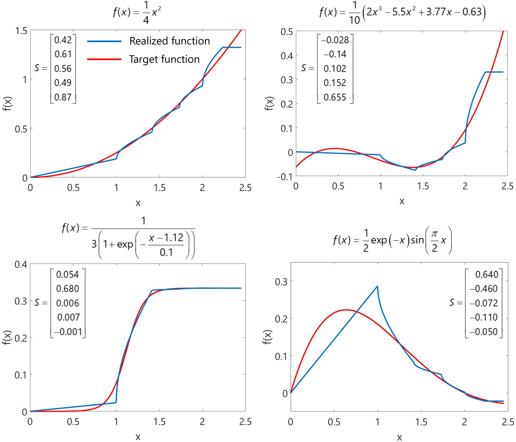
Examples of different target nonlinear functions of the input signal by our proposed reconfigurable nonlinear element shown in Figure 2(a). Red curves are the target functions of the input signal the expression of which are shown at top of the plots. The blue curves are the resulting functions from our proposed element, by optimizing the scales of the slope screen using minimization of the MSE error between target and realized functions. The inset in each panel shows the optimized scales of the corresponding realized function.
4 Summary and conclusions
In this work, we theoretically proposed and numerically demonstrated a device that can exhibit reconfigurable nonlinear dependence between the input and output signals. It consists of two networks, the first of which is a set of several identical inverse-designed three-port structures with an optimized mixture of linear and nonlinear materials, providing desired power limiting and power dividing characteristics. The second network is a linear mesh of MZI elements that consists of two sections; the slope screen and the adder networks. The reconfigurability of the MZI mesh enables one to change and tune the functional dependence of the entire device at will. Several examples illustrating salient features of this device were given and discussed. The fact that the proposed architecture is reconfigurable makes it useful for numerous applications such as optical neural networks and wave-based analog computing architectures with nonlinearity.
Funding source: National Science Foundation
Award Identifier / Grant number: DMR-1720530
Funding source: Air Force Office of Scientific Research
Award Identifier / Grant number: FA9550-17-1-0002
Award Identifier / Grant number: FA9550-21-1-0312
-
Author contributions: All authors have accepted responsibility for the entire content of this manuscript and approved its submission.
-
Research funding: This work is supported in part by the US Air Force Office of Scientific Research (AFOSR) Multidisciplinary University Research Initiative (MURI) grant numbers FA9550-17-1-0002 and FA9550-21-1-0312, and in part by the US National Science Foundation (NSF) MRSEC program under award No. DMR-1720530.
-
Conflict of interest statement: The authors declare no conflicts of interest.
-
Data Availability Statement: The datasets generated and/or analyzed during the current study are available from the corresponding author upon reasonable request.
References
[1] X. Guo, C.-L. Zou, H. Jung, and H. X. Tang, “On-chip strong coupling and efficient frequency conversion between telecom and visible optical modes,” Phys. Rev. Lett., vol. 117, no. 12, p. 123902, 2016. https://doi.org/10.1103/physrevlett.117.123902.Search in Google Scholar
[2] Y. Jiang, P. T. DeVore, and B. Jalali, “Analog optical computing primitives in silicon photonics,” Opt. Lett., vol. 41, no. 6, pp. 1273–1276, 2016. https://doi.org/10.1364/ol.41.001273.Search in Google Scholar PubMed
[3] M. Lapine, I. V. Shadrivov, and Y. S. Kivshar, “Colloquium: nonlinear metamaterials,” Rev. Mod. Phys., vol. 86, no. 3, p. 1093, 2014. https://doi.org/10.1103/revmodphys.86.1093.Search in Google Scholar
[4] A. Krasnok, M. Tymchenko, and A. Alù, “Nonlinear metasurfaces: a paradigm shift in nonlinear optics,” Mater. Today, vol. 21, no. 1, pp. 8–21, 2018. https://doi.org/10.1016/j.mattod.2017.06.007.Search in Google Scholar
[5] Y. Shen, N. C. Harris, S. Skirlo, et al.., “Deep learning with coherent nanophotonic circuits,” Nat. Photonics, vol. 11, no. 7, pp. 441–446, 2017. https://doi.org/10.1038/nphoton.2017.93.Search in Google Scholar
[6] R. Hamerly, L. Bernstein, A. Sludds, M. Soljačić, and D. Englund, “Large-scale optical neural networks based on photoelectric multiplication,” Phys. Rev. X, vol. 9, no. 2, p. 021032, 2019. https://doi.org/10.1103/physrevx.9.021032.Search in Google Scholar
[7] A. Krizhevsky, I. Sutskever, and G. E. Hinton, “Imagenet classification with deep convolutional neural networks,” Commun. ACM, vol. 60, no. 6, pp. 84–90, 2012. https://doi.org/10.1145/3065386.Search in Google Scholar
[8] T. Young, D. Hazarika, S. Poria, and E. Cambria, “Recent trends in deep learning based natural language processing,” IEEE Comput. Intell. Mag., vol. 13, no. 3, pp. 55–75, 2018. https://doi.org/10.1109/mci.2018.2840738.Search in Google Scholar
[9] M. M. Najafabadi, F. Villanustre, T. M. Khoshgoftaar, N. Seliya, R. Wald, and E. Muharemagic, “Deep learning applications and challenges in big data analytics,” J. Big Data, vol. 2, no. 1, pp. 1–21, 2015. https://doi.org/10.1186/s40537-014-0007-7.Search in Google Scholar
[10] D. Silver, T. Hubert, J. Schrittwieser, et al.., “A general reinforcement learning algorithm that masters chess, shogi, and go through self-play,” Science, vol. 362, no. 6419, pp. 1140–1144, 2018. https://doi.org/10.1126/science.aar6404.Search in Google Scholar PubMed
[11] D. Wang, A. Khosla, R. Gargeya, H. Irshad, and A. H. Beck, “Deep learning for identifying metastatic breast cancer,” arXiv preprint arXiv:1606.05718, 2016.Search in Google Scholar
[12] B. Karlik and A. V. Olgac, “Performance analysis of various activation functions in generalized mlp architectures of neural networks,” Int. J. Artif. Intell. Expert Syst., vol. 1, no. 4, pp. 111–122, 2011.Search in Google Scholar
[13] N. C. Harris, J. Carolan, D. Bunandar, et al.., “Linear programmable nanophotonic processors,” Optica, vol. 5, no. 12, pp. 1623–1631, 2018. https://doi.org/10.1364/optica.5.001623.Search in Google Scholar
[14] M. P. Bendsoe and O. Sigmund, Topology Optimization: Theory, Methods, and Applications, 2nd ed. Berlin/Heidelberg, Springer Science & Business Media, 2003.Search in Google Scholar
[15] J. Lu, S. Boyd, and J. Vučković, “Inverse design of a three-dimensional nanophotonic resonator,” Opt. Express, vol. 19, no. 11, pp. 10563–10570, 2011. https://doi.org/10.1364/oe.19.010563.Search in Google Scholar PubMed
[16] A. Y. Piggott, J. Lu, K. G. Lagoudakis, J. Petykiewicz, T. M. Babinec, and J. Vučković, “Inverse design and demonstration of a compact and broadband on-chip wavelength demultiplexer,” Nat. Photonics, vol. 9, no. 6, pp. 374–377, 2015. https://doi.org/10.1038/nphoton.2015.69.Search in Google Scholar
[17] A. Y. Piggott, J. Petykiewicz, L. Su, and J. Vučković, “Fabrication-constrained nanophotonic inverse design,” Sci. Rep., vol. 7, no. 1, pp. 1–7, 2017. https://doi.org/10.1038/s41598-017-01939-2.Search in Google Scholar PubMed PubMed Central
[18] S. Molesky, Z. Lin, A. Y. Piggott, W. Jin, J. Vucković, and A. W. Rodriguez, “Inverse design in nanophotonics,” Nat. Photonics, vol. 12, no. 11, pp. 659–670, 2018. https://doi.org/10.1038/s41566-018-0246-9.Search in Google Scholar
[19] T. W. Hughes, M. Minkov, I. A. Williamson, and S. Fan, “Adjoint method and inverse design for nonlinear nanophotonic devices,” ACS Photonics, vol. 5, no. 12, pp. 4781–4787, 2018. https://doi.org/10.1021/acsphotonics.8b01522.Search in Google Scholar
[20] D. A. Miller, “Sorting out light,” Science, vol. 347, no. 6229, pp. 1423–1424, 2015. https://doi.org/10.1126/science.aaa6801.Search in Google Scholar PubMed
[21] D. A. Miller, “Establishing optimal wave communication channels automatically,” J. Lightwave Technol., vol. 31, no. 24, pp. 3987–3994, 2013. https://doi.org/10.1109/jlt.2013.2278809.Search in Google Scholar
[22] D. A. Miller, “Self-aligning universal beam coupler,” Opt. Express, vol. 21, no. 5, pp. 6360–6370, 2013. https://doi.org/10.1364/oe.21.006360.Search in Google Scholar
[23] C. Taballione, T. A. Wolterink, J. Lugani, et al.., “8× 8 reconfigurable quantum photonic processor based on silicon nitride waveguides,” Opt. Express, vol. 27, no. 19, pp. 26842–26857, 2019. https://doi.org/10.1364/oe.27.026842.Search in Google Scholar PubMed
[24] W. Bogaerts, D. Pérez, J. Capmany, et al.., “Programmable photonic circuits,” Nature, vol. 586, no. 7828, pp. 207–216, 2020. https://doi.org/10.1038/s41586-020-2764-0.Search in Google Scholar PubMed
[25] N. C. Harris, G. R. Steinbrecher, M. Prabhu, et al.., “Quantum transport simulations in a programmable nanophotonic processor,” Nat. Photonics, vol. 11, no. 7, pp. 447–452, 2017. https://doi.org/10.1038/nphoton.2017.95.Search in Google Scholar
[26] M. Reck, A. Zeilinger, H. J. Bernstein, and P. Bertani, “Experimental realization of any discrete unitary operator,” Phys. Rev. Lett., vol. 73, no. 1, p. 58, 1994. https://doi.org/10.1103/physrevlett.73.58.Search in Google Scholar
[27] D. A. Miller, “Self-configuring universal linear optical component,” Photonics Res., vol. 1, no. 1, pp. 1–15, 2013. https://doi.org/10.1364/prj.1.000001.Search in Google Scholar
[28] W. R. Clements, P. C. Humphreys, B. J. Metcalf, W. S. Kolthammer, and I. A. Walmsley, “Optimal design for universal multiport interferometers,” Optica, vol. 3, no. 12, pp. 1460–1465, 2016. https://doi.org/10.1364/optica.3.001460.Search in Google Scholar
[29] V. Nikkhah, D. C. Tzarouchis, A. Hoorfar, and N. Engheta, “Inverse-designed metastructures together with reconfigurable couplers to compute forward scattering,” ACS Photonics, vol. 10, no. 4, pp. 977–985, 2022. https://doi.org/10.1021/acsphotonics.2c00373.Search in Google Scholar
[30] M. J. Mencagli, N. M. Estakhri, B. Edwards, and N. Engheta, “Solving equations with waves in collections of mach-zehnder interferometers,” in 2018 Conference on Lasers and Electro-Optics (CLEO), IEEE, 2018, pp. 1–2.10.1364/CLEO_QELS.2018.FF3C.3Search in Google Scholar
[31] D. C. Tzarouchis, M. J. Mencagli, B. Edwards, and N. Engheta, “Mathematical operations and equation solving with reconfigurable metadevices,” Light: Sci. Appl., vol. 11, no. 1, pp. 1–13, 2022. https://doi.org/10.1038/s41377-022-00950-1.Search in Google Scholar PubMed PubMed Central
[32] R. W. Boyd, Nonlinear Optics, 3rd ed. Cambridge, Massachusetts, Academic Press, 2008.Search in Google Scholar
[33] P. Xing, D. Ma, K. J. Ooi, J. W. Choi, A. M. Agarwal, and D. Tan, “Cmos-compatible pecvd silicon carbide platform for linear and nonlinear optics,” ACS Photonics, vol. 6, no. 5, pp. 1162–1167, 2019. https://doi.org/10.1021/acsphotonics.8b01468.Search in Google Scholar
[34] D. A. Miller, “Perfect optics with imperfect components,” Optica, vol. 2, no. 8, pp. 747–750, 2015. https://doi.org/10.1364/optica.2.000747.Search in Google Scholar
Supplementary Material
This article contains supplementary material (https://doi.org/10.1515/nanoph-2023-0152).
© 2023 the author(s), published by De Gruyter, Berlin/Boston
This work is licensed under the Creative Commons Attribution 4.0 International License.
Articles in the same Issue
- Frontmatter
- Editorial
- Nanophotonics in support of Ukrainian Scientists
- Reviews
- Asymmetric transmission in nanophotonics
- Integrated circuits based on broadband pixel-array metasurfaces for generating data-carrying optical and THz orbital angular momentum beams
- Singular optics empowered by engineered optical materials
- Electrochemical photonics: a pathway towards electrovariable optical metamaterials
- Sustainable chemistry with plasmonic photocatalysts
- Perspectives
- Ukraine and singular optics
- Machine learning to optimize additive manufacturing for visible photonics
- Through thick and thin: how optical cavities control spin
- Research Articles
- Spin–orbit coupling induced by ascorbic acid crystals
- Broadband transfer of binary images via optically long wire media
- Counting and mapping of subwavelength nanoparticles from a single shot scattering pattern
- Controlling surface waves with temporal discontinuities of metasurfaces
- On the relation between electrical and electro-optical properties of tunnelling injection quantum dot lasers
- On-chip multivariant COVID 19 photonic sensor based on silicon nitride double-microring resonators
- Nano-infrared imaging of metal insulator transition in few-layer 1T-TaS2
- Electrical generation of surface phonon polaritons
- Dynamic beam control based on electrically switchable nanogratings from conducting polymers
- Tilting light’s polarization plane to spatially separate the ultrafast nonlinear response of chiral molecules
- Spin-dependent phenomena at chiral temporal interfaces
- Spin-controlled photonics via temporal anisotropy
- Coherent control of symmetry breaking in transverse-field Ising chains using few-cycle pulses
- Field enhancement of epsilon-near-zero modes in realistic ultrathin absorbing films
- Controlled compression, amplification and frequency up-conversion of optical pulses by media with time-dependent refractive index
- Tailored thermal emission in bulk calcite through optic axis reorientation
- Tip-enhanced photoluminescence of monolayer MoS2 increased and spectrally shifted by injection of electrons
- Quantum-enhanced interferometer using Kerr squeezing
- Nonlocal electro-optic metasurfaces for free-space light modulation
- Dispersion braiding and band knots in plasmonic arrays with broken symmetries
- Dual-mode hyperbolicity, supercanalization, and leakage in self-complementary metasurfaces
- Monocular depth sensing using metalens
- Multimode hybrid gold-silicon nanoantennas for tailored nanoscale optical confinement
- Replicating physical motion with Minkowskian isorefractive spacetime crystals
- Reconfigurable nonlinear optical element using tunable couplers and inverse-designed structure