2D layered MSe2 (M = Hf, Ti and Zr) for compact lasers: nonlinear optical properties and GHz lasing
-
Genglin Li
 ,
Yandong Ma
,
Yandong Ma
 ,
Yuechen Jia
and
Feng Chen
,
Yuechen Jia
and
Feng Chen

Abstract
Two-dimensional (2D) ternary transition-metal dichalcogenides (TMDCs) are of great research interest because their superior layer-dependent optical modulation properties. In this work, three different kinds of TMDC nanosheets, including hafnium diselenide (HfSe2), titanium diselenide (TiSe2) and zirconium diselenide (ZrSe2), are prepared by liquid phase exfoliation (LPE) technique. The high-quality material properties of these TMDC nanosheets are confirmed by Raman spectroscopy and X-ray diffraction analysis. Furthermore, the bandgap information of five-layer MSe2 has been investigated via utilizing density functional theory. The calculation results exhibit ultra-narrow bandgap structure (lower than 1.1 eV) for all these three materials, indicating that MSe2 is suitable for broadband photonic applications. By applying the fabricated MSe2 as saturable absorbers, high-performance Q-switched mode-locked laser operation has been realized. The laser gain media are Nd:GdVO4 cladding waveguides fabricated by femtosecond laser direct writing. As a result, the pulsed waveguide lasers are able to deliver approximately 6-GHz laser pulses with a signal-to-noise ratio of over 45 dB. The minimum pulse width is determined to be as short as 26 ps. The results demonstrated in this work exhibit the great potential of TMDCs and waveguide structures in applications of pulsed lasers with compact footprints.
1 Introduction
Integrated photonics, as a fundamental for researching monolithic integration between optical devices and optoelectronic systems, plays a crucial role in promoting the emergence of quantum communication, light manipulation, and multi-functional photonic chips [1–3]. Through combining high-efficiency and broadband-response optical modulators with integrated photonic circuits, efficient on-chip modulation and fast transmission of optical signals can be realized [4–6]. Therefore, plenty of research efforts are devoted to exploring high-performance optical modulators based on all-optical [7, 8] or electro-optic solutions [9, 10]. It is widely acknowledged that two-dimensional (2D) materials, profiting by their flexible and multi-functional properties (especially ultrafast broadband optical modulation features), are extensively employed as efficient optical modulators in micro-/nano-photonics and integrated photonic devices. These layered materials are able to enrich the functionality of photonic devices and open up new possibilities for future photonic chips [11–13].
Transition metal dichalcogenides (TMDCs), as an important category of 2D materials, possess thermodynamically stable and sandwich-shaped layered structures. Therefore, these 2D materials can be fabricated into few-layer or even single-layer structures via various techniques, for instance, chemical vapor deposition (CVD) [14], pulsed laser deposition (PLD) [15], liquid phase exfoliation (LPE) [16], etc. TMDCs have the general formula MX2, where M represents transition metals (elements in groups IV, V or VI) and X refers to chalcogenides (S, Se or Te). Their crystal structures have the CdI2-type configuration in which an inner transition metal atom is coordinated by six chalcogen atoms, forming an octahedron structure [17]. Benefitting from their flexible layer structures, the bandgaps of TMDCs are generally over 1.0 eV, which can be varied from metal (multi-later) to semiconductor (monolayer) by adjusting the layer quantity [15, 18]. Their unique bandgap structures endow TMDCs with desirable optical modulation properties, which can be used as saturable absorbers (SAs) in pulsed laser generation.
Hafnium diselenide (HfSe2), as a newly-manufactured TMDC member, has a bandgap of around 1.11-eV, demonstrating effective optical absorption at the near-infrared (NIR) wavelengths [19, 20]. According to the previously reported work, the modulation depth of HfSe2 measured by I-scan technique is 5.8% [21], which is around 30 times higher than that of MoS2 [22]. Titanium diselenide (TiSe2) is one of the novel metal–insulator transition materials in TMDC family. It offers ultrafast nonlinear optical response and significantly compact bandgap (only 0.15 eV) [23]. Remarkably, some researchers have theoretically calculated the band structure of monolayer TiSe2, demonstrating a zero-bandgap structure similar to graphene and thus suggesting its great potential in broadband optical modulation applications [24]. Zirconium diselenide (ZrSe2) with a CdI2 (1T) structure presents lower than 1-eV indirect bandgap, which means that it has the potential to be utilized as a promising broadband SA in ultrafast laser generation [25, 26]. Although several bulk or fiber laser works based on these materials as SAs have been reported, there is still lacking of through investigations on their saturable absorption properties under multi-GHz pulsed laser operation. In addition, both bulk and fiber laser arrangements lack the ability of on-chip integration. As the counterpart of MSe2, MS2 (including HfS2, TiS2 and ZrS2) has similar crystal structures. In comparison, MS2 generally possesses larger bandgaps and stronger interlayer interaction originating from the higher electronegativity of sulfur element [27–29]. These properties make MS2 difficult to be separated into monolayer structure and limit their applications in the infrared bands [30].
In contrast to bulk and fiber lasers, waveguide lasers with compact and robust packages are highly compatible with on-chip photonic integration. Benefitting from the compact structures of optical waveguides, waveguide lasers combine the respective merits of strong mode confinement and preferable mode overlapping [31–33], thereby offering lower lasing threshold and higher intracavity optical gain compared with other laser configurations [34–37]. As a result, through combining the flexibility of waveguide structures with the desirable optoelectronic properties of 2D materials, compact pulsed lasers delivering multi-GHz pulses can be fabricated. Furthermore, by applying external modulation methods, such as electric field, on the 2D materials, tunable SA properties and thus lasing performance can be expected [38, 39]. This can be also possible for the “waveguide + 2D material” configuration by depositing micro-/nano-electrodes on the 2D material surface. A very compact strategy uses waveguide structures and 2D materials both defined on the substrate surfaces, for which the interaction between SA and guided laser modes is supported by the evanescent field [40].
In this work, we successfully fabricate HfSe2, TiSe2 and ZrSe2 nanosheets on sapphire substrates via LPE and spin coating methods. Their bandgaps, corresponding to the layer quantity of N = 5, are systematically analyzed using density functional theory (DFT). The nonlinear saturable absorption properties of these 2D layered materials are investigated by Z-scan and I-scan analysis, respectively. Modulated by these 2D layered materials, passively Q-switched mode-locked (QML) waveguide laser with a minimum pulse width of 26 ps and a repetition rate of 6.31 GHz is obtained.
2 Preparation and characterization of TMDCs
2.1 Thin-film TMDC preparation
Compared with other 2D layered material preparation methods, such as CVD, LPE is relatively cost-effective and less time-consuming [41]. Here, LPE technique is used for preparation of the thin-film TMDCs. In order to fabricate large-scale few-layer SAs, in the first step, mechanical milling is employed to process bulk materials (supplied by 6Carbon Technology, China) into powder for promoting the 2D material powder dissolving in solvents. Subsequently, LPE and ultrasonic centrifugation techniques are used to further reduce the layer quantity of 2D materials. The MSe2 (M = Hf, Ti and Zr) powder is dissolved in ethanol and sonicated for 10 h. The duration of this process depends on the interlayer interactions within materials. In general, the lower the interlayer binding energy, the shorter sonication time required [42]. Then, the MSe2 mixed solution is centrifuged at a fixed 10,000-rpm rotating speed for 10 min, aiming to remove impurities and ethanol insoluble fractions. We extract the supernatant of suspension, in which dissolved MSe2 powders possessing few-layer even monolayer morphologies, and transfer them onto the sapphire substrate surface (10 × 10 mm2). The obtained precipitates are placed in a vacuum oven at 60 °C for 2 h to evaporate ethanol solvent. Finally, the sample surface is spin-coated with a layer of polymethyl methacrylate (PMMA) as the protective layer to prevent the inner few-layer MSe2 from being oxidized. In this way, large-scale few-layer MSe2 SAs are successfully fabricated.
2.2 Materials characterization
Figure 1(a)–(c) demonstrate the morphological properties of MSe2 powder after physical grinding characterized by scanning electron microscopy (SEM). According to the SEM images, the geometries of the bulk materials have been significantly reduced, maintaining a horizontal size of several micrometers. The surface topography and height information of the prepared few-layer MSe2 nanosheets are analyzed via atom force microscopy (AFM), as illustrated in Figure 1(d)–(f). It can be observed in Figure 1(g)–(i) that the thicknesses of HfSe2, TiSe2 and ZrSe2 samples are 3.3, 3.2 and 3.2 nm, respectively. According to the previously reported average monolayer thicknesses of 0.62, 0.601, and 0.615 nm, respectively, for these materials [20, 43, 44], the thicknesses determined in this work are equivalent to the layer quantity of approximately five in all cases. Therefore, the processing parameters used in this work are favorable for the preparation of high-quality MSe2 materials with several-micrometer lateral sizes and few-layer thicknesses.

Characterization of prepared 2D MSe2 samples.
(a)–(c) SEM images of HfSe2, TiSe2 and ZrSe2 powders after physical grinding. (d)–(i) AFM pictures and the height variations in white line scanning region, corresponding to HfSe2, TiSe2 and ZrSe2 nanosheets fabricated by LPE method.
From the Raman spectra (see Figure 2(a)–(c)) collected from all the TMDCs prepared in this work, two typical spectral peaks, which respectively represent in-plane (E g) and out-of-plane (A g) Raman active modes, can be identified in the range of 100–300 cm−1 under 1064-nm laser excitation. These results are consistent with previously reported works [19, 23, 25]. The X-ray diffraction (XRD) results of MSe2, as demonstrated in Figure 2(d)–(f), show that the MSe2 powder has favorable hexagonal structure and good crystallinity, which are beneficial for the preparation of few-layer 2D materials during the subsequent LPE process. The XRD pattern of HfSe2 in Figure 2(d) is consist with a hexagonal structure (PDF#04-004-1183), while the strong (001) orientation is associated with a diffraction angle (2θ) of 14.369°. Compared with the other two materials, the XRD pattern of HfSe2 demonstrates the fewest diffraction peaks, affirming that the layer quantity of HfSe2 powder has been significantly reduced to few layers after grinding. The (001), (002), (003) and (004) diffraction peaks of TiSe2 depicted in Figure 2(e) match well with a CdI2 (1T) structure (PDF#04-003-3838). The typical diffraction peaks of ZrSe2 in Figure 2(f) are in common with 1T-ZrSe2 (PDF#04-003-5768), which means the lattice structure of material remain undamaged after grinding process. In comparison, more diffraction peaks in the ZrSe2 case could be attributed to the insufficient purity during bulk material preparation or oxidization due to the material instability and the layer stacking during characterization processes.

Raman spectral and XRD analysis.
(a)–(c) Raman spectrums of HfSe2, TiSe2 and ZrSe2 sample. (d)–(e) XRD patterns of MSe2 samples, the colored (red, blue and green) lines are experimental data and the black line represents standard PDF card.
2.3 Theoretical calculation
In order to theoretically characterize the bandgap of prepared five-layer MSe2 samples through LPE method (confirmed by AFM results in Section 2.2), we employ density functional theory (DFT) calculation based on the Vienna ab initio Simulation Package (VASP). During the calculation process, Perdew–Burke–Ernzerhof (PBE) of generalized gradient approximation function is chosen for exchange–correlation interaction. The cut-off energy of kinetic is set as 450 eV. The convergence criteria for energy and force are fixed at 10−5 eV and 0.01 eV/Å, respectively. A Brillouin zone is sampled by Monkhorst–Pack method with a k-point grid of 17 × 17 × 1. The vacuum along z-axis is set to 50 Å for avoiding spurious interlayer interactions. To include the strong correlation effects, the “GGA + U” method is adopted with the U eff of 5, 3.9 and 5 eV for Hf, Ti and Zr atoms, respectively, following the previous works [29, 45, 46]. Figure 3 demonstrates the band structures of five-layer MSe2. We can observe that the bandgaps of HfSe2, TiSe2 and ZrSe2 are 1.07, 0 and 0.95 eV, corresponding to optical absorption at over 1-µm wavelengths. Thus, the calculation results confirm that all these three materials possess optical absorption properties in the NIR region. Besides the zero-bandgap material of TiSe2, the bandgaps of HfSe2 and ZrSe2 with different layer quantities are theoretically calculated in previously reported works [27, 29], demonstrating layer-dependent bandgaps, and thus layer-dependent optical properties.

Band structure calculation.
(a) Top view and crystal structure of five layers MSe2 materials. First-principles simulations of the five-layer MSe2 band structures. Calculated electronic band structures of the five-layer (b) HfSe2, (c) TiSe2 and (d) ZrSe2.
2.4 Optical and nonlinear absorption properties
The linear optical absorption properties of the prepared samples are characterized by a Shimadzu UV-3600 spectrophotometer, as demonstrated in Figure 4(a)–(c). The optical absorbance values of the prepared MSe2 are all higher than 0.28 at 1.06 μm, suggesting that the potential of these 2D layered materials for nonlinear optical absorption applications. By utilizing the open-aperture Z-scan technique, the nonlinear optical absorption properties of the prepared MSe2 samples at 1.03-μm wavelength are characterized. In the home-built Z-scan setup, a 1035-nm mode-locked fiber laser (Femto YL-10, YSL Photonics, China) is used, which provides 400-fs pulse duration, 400-μJ maximum pulse energy and 25-kHz to 5-MHz tunable repetition rate. The laser beam with a waist radius of ∼60 μm is focused on the surface of prepared MSe2 samples. During the measurement, the prepared SA samples are placed at a PC-controlled motorized stage moving along the laser beam direction (z-axis). The incident and transmitted light power are monitored by two power meters simultaneously. As the sample moves toward the focal point (z = 0), the energy density irradiated on sample surface increases continuously while the normalized transmittance curve becomes sharp, which means that the optical absorption starts to saturate.

Linear and nonlinear optical properties.
(a)–(c) Optical absorption spectrums of HfSe2, TiSe2 and ZrSe2 on sapphire substrate. (d)–(e) Open-aperture (OA) Z-scan results of MSe2 based SAs under 1035-nm laser excitation (g)–(i) The intensity dependent nonlinear transmittances of few-layer HfSe2, TiSe2 and ZrSe2 nanosheets at 1035 nm.
The normalized transmittance curves with approximately symmetrical shapes (centered at the focal point) are demonstrated in Figure 4(d)–(f), and the peak values at z = 0 position confirms that the MSe2-based samples possess favorable optical modulation properties. The fluctuation of the experimental data primarily originates from the inhomogeneity of material distribution on substrate surface. Nevertheless, we can obtain the modulation depth and the saturation intensity of materials through fitting the normalized experimental data (transmittance as a function of coordinate position) according to the following formula [47],
where T represents the normalized transmittance, ΔR stands for the modulation depth, I 0 and I s are the incident and saturable intensity, respectively. Z 0 is the Rayleigh length of incident laser beam. As a result, the modulation depths of MSe2 are simulated to be 6.9% (HfSe2), 5.4% (TiSe2) and 6.3% (ZrSe2) and the saturable intensities are 0.49 mJ/cm2 (HfSe2), 0.12 mJ/cm2 (TiSe2) and 0.19 mJ/cm2 (ZrSe2), respectively.
Furthermore, by increasing the incident light power, the optical transmittance of the MSe2 materials tends to be saturated at certain values, confirming their saturable absorption properties, see Figure 4(g)–(i) (namely, I-scan analysis). The experimental transmittance curves are fitted by using the following formula [48],
where T, ΔR, I s and T ns are the transmittance rate, modulation depth, saturable intensity and nonsaturable loss, respectively. Under the I-scan model, the modulation depths are determined to be 7.3% for HfSe2, 5.7% for TiSe2 and 6.8% for ZrSe2. The fitting results are close to the Z-scan test, confirming that the MSe2 prepared in this work have the potential to be used as SA elements.
3 Q-switched mode-locked waveguide laser
In order to experimentally verify the saturable absorption properties of the prepared MSe2 samples, we utilized them as SAs in a waveguide laser configuration. The active gain medium used here is a Nd:GdVO4 cladding waveguide fabricated by FsLDW (the waveguide loss information can be found in the Supplementary material), detailed information of this technique for waveguide fabrication can be referenced elsewhere [33]. The pulsed laser generation has been investigated by a typical end-face coupling system, as illustrated in Figure 5 (the inset shows the cross-sectional image of the fabricated waveguide structure), in which a tunable continuous wave (CW) Ti:sapphire laser (Coherent MBR-110) is employed for optical pumping. The linearly-polarized 813-nm pump light is applied for the generation of 1063-nm pulsed laser. By means of combining a plano-convex lens (with a focal length of 25 mm) and a microscope objective lens (20×, N.A. = 0.4), the pump light and generated pulsed laser can be coupled into/out of the cladding waveguide. For the Q-switched mode-locked waveguide laser configuration, the Fabry–Perot cavity is mainly composed by three elements, namely, a pump mirror (PM), the laser crystal sample (attached with SAs), and an output coupler (OC). The PM provides a high transmittance of >99.8% at 808 nm and a high reflectivity of >99.99% at 1064 nm. The inner facet of OC coated by a part-reflection layer maintains around 40% at 1064 nm, whereas the outer surface of it provides anti-reflection (<0.25%) at 1064 nm. A long-pass filter (Thorlabs, FEL 900) is applied to eliminate the residual pump light. The filtered laser is collected by another objective lens (25|× N.A. = 0.4), aiming to couple the pulsed laser into a single-mode fiber connected directly to the High-Speed Fiber-Optic Photodetector (New focus, 1414 model). Each component in the waveguide laser setup is placed on three five-dimensional translation optical stages separately, ensuring the relative position of each part can be flexibly adjusted to achieve the best coupling conditions. Ultimately, the captured Q-switched mode-locked laser is observed on a digital oscilloscope (Tektronix, MSO 72504DX).
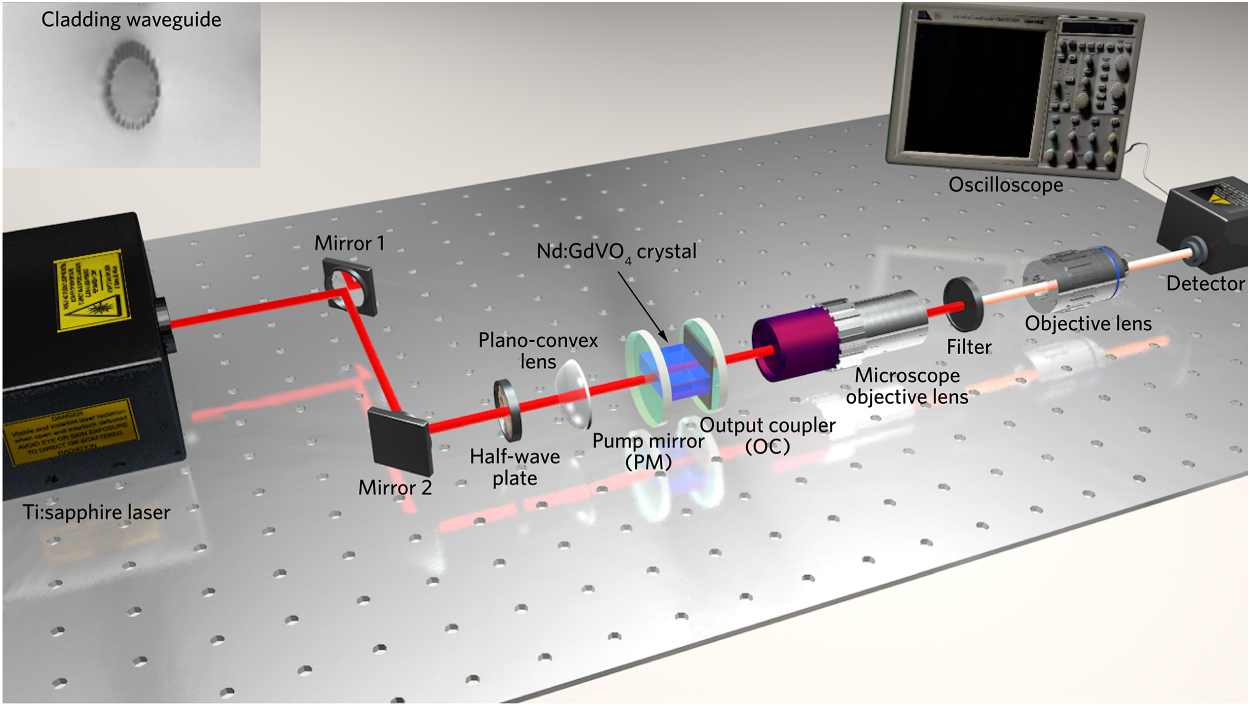
Schematic diagram of the typical end-face coupling facility for pulsed laser delivery. The inset is waveguide structure (upper-left).
3.1 Q-switched mode-locked laser operated by HfSe2
To further investigate the saturable absorption response of HfSe2, we insert the prepared HfSe2 sample (approximately five layers made by LPE) between the OC and the output facet of the cladding waveguide. The Q-switched mode-locked laser performance based on HfSe2 SA has been demonstrated in Figure 6(a)–(d). The measured mode profiles of pulsed laser (see Figure 6(a) insets) confirm single-mode transmission, which is beneficial to reduce the intracavity losses. As depicted in Figure 6(a), the maximum power of pulsed laser is measured to be 255.5 mW (152.7 mW) under optical pumping with TE (TM) polarization. The Q-switched mode-locked laser can be achieved when the pump power is increased to 90.5 mW (94.9 mW). Figure 6(b) demonstrates the typical Q-switched envelope composed of mode-locked sequences delivering a pulse duration of 160 ns. The inset of Figure 6(b) displays the Q-switched trains on nanosecond (100 ns/div). Figure 6(c) illustrates the mode-locked trains on picosecond (400 ps/div) generated by utilizing HfSe2 as SA, while the measured full width half maximum (FWHM) of an individual pulse is determined to be 30 ps (see Figure 6(d)). The radio frequency (RF) spectrum in the upper-left of Figure 6(d) depicts the fundamental repetition of 6.12 GHz and the signal-to-noise ratio (SNR) of 45 dB, confirming the stability of the waveguide laser operation. It is noteworthy that our experimental results shown in Figure 6(a)–(d) have relatively narrow pulse width (∼30 ps) and high repetition frequency (over 6 GHz) simultaneously, suggesting the excellent nonlinear optical properties of HfSe2 SA for applications in ultrafast optical modulation.

Q-switched mode-locked laser generated by inserting HfSe2 as SA.
(a) The dependence between the pump power and the output pulsed laser power. The inset depicts the pulsed laser modes with TE and TM polarizations. (b) A single Q-switched envelope and the inset illustrates pulse trains. (c) Mode-locked pulse sequence with picosecond timescale. (d) Single mode-locked trace of output pulsed laser. The upper-left shows the radio frequency spectrum of output pulsed laser.
3.2 Q-switched mode-locked laser operated by TiSe2
Through replacing the HfSe2 SA by the TiSe2 SA, subsequently, pulsed waveguide lasers with similar performance can be achieved (see Figure 7(a)). The maximum output power is determined to be 261.9 mW (162.1 mW) and the slope efficiency is calculated to be 28.4% (18.3%) for TE (TM) mode, respectively. When the pump power exceeds over 90 mW, a stable Q-switched mode-locked laser can be observed. For nanosecond timescale Q-switched envelope demonstrated in Figure 7(b), the single pulse energy is determined to be 47.6 nJ, corresponding to a peak power of 0.48 W. Figure 7(c) and (d) illustrate the mode-locked pulse trains and the single pulse profile on picosecond timescale (200 ps/div), in which the minimum pulse width as short as 26 ps has achieved, confirming the ability of TiSe2 as a promising SA for ultrashort pulse laser generation. The inset of Figure 7(f) records the RF spectra of TiSe2 based pulsed laser, evidently, a sharp peak is identified at 6.31 GHz, corresponding to a SNR of 51 dB. During the experiment, there is no obvious optical damage to the TiSe2-SA.

Q-switched mode-locked laser modulated by TiSe2.
(a) Pulsed laser power as a function of pump power (the inset demonstrating the profiles of TE and TM modes). (b) A single Q-switched envelope and the inset illustrates pulse trains. (c) Mode-locked pulse sequence with picosecond timescale. (d) Single mode-locked trace of output pulsed laser and radio frequency spectrum of output pulsed laser.
3.3 Q-switched mode-locked laser operated by ZrSe2
At last, Q-switched mode-locked laser operation has also been investigated through inserting ZrSe2-SA into the waveguide cavity. As shown in Figure 8(a), single-mode laser operation has achieved in the waveguide structure when the pump power increases over 90.6 mW (95.5 mW) threshold. The maximum output power of 245.1 mW (129.4 mW) is obtained, corresponding to the pump power of 1.013 W. In contrast to the abovementioned HfSe2 and TiSe2 based lasers, the slightly inferior performance can be attributed to the partial oxidation of ZrSe2 sample, which has been discussed in Section 2. Figure 8(b) demonstrates a single Q-switched envelope composed by a serious of mode-locked pulses. The mode-locked pulse trains on the timescale of 400 ps/div are depicted in Figure 8(c). A minimum pulse duration of 38 ps is illustrated in Figure 8(d). An obvious peak located at 6.34 GHz with a SNR reaching about 46 dB is recorded in RF spectrum, as depicted in Figure 8(d).

ZrSe2-SA based Q-switched mode-locked laser.
(a) Linear relationship between pump power and output pulsed laser power, and the pulsed laser modes under TE and TM polarizations (down-right). (b) The measured single Q-switched envelope and the inset depicts the pulse trains. (c) Mode-locked pulse sequence with picosecond timescale. (d) Characterized single mode-locked trains of output pulsed laser and recorded radio frequency of the output pulsed laser.
4 Discussion
Up to now, several works related to HfSe2 SA in different laser configurations have been reported. For example, one work realized 18.1-MHz repetition rate continuous-wave mode-locked (CWML) operation in the 1.5-μm spectral region [21] and another demonstrated a Q-switched laser with 2.4-μs pulse width emission at 1060 nm [49]. In contrast, our experimental results shown in Figure 6(d) have a relatively narrow pulse width (∼30 ps) and a high repetition frequency (over 6 GHz) simultaneously. In addition, combining a 26-ps pulse duration with gigahertz repetition rate, the performance of Q-switched mode-locked waveguide laser is superior to the previously reported value of Q-switched Nd:GdVO4 laser obtained using SA based on TiSe2 [43]. Consequently, the approximately 6-GHz repetition rate and high-SNR (over 45 dB) waveguide laser performance in this work are comparable to those of the solid-state or fiber lasers using SAs based on TMDCs [50, 51], which means that our waveguide laser system has the potential to achieve CWML operation by further implementing efficient dispersion management [34]. Furthermore, we have also investigated the stability of the laser performance under stable optical pumping for over 1-hour time scale. As a result, only 10–15% of fluctuations on the pulse intensities can be identified for all cases, suggesting the good stability of the waveguide lasers demonstrated in this work.
The Q-switched mode-locked laser performance based on different TMDCs as saturable absorbers are summarized in Table 1. The fascinating pulsed laser operation based on waveguide structure can be ascribed to the excellent nonlinear optical responses of MSe2 (M = Hf, Ti and Zr) samples. In contrast to CVD or other material growing methods, LPE combined with spin-coating method enables the mass production of few-layer nanomaterials in a short period of time [52]. Whereas, LPE technique is hard to control the large scale (over millimeters) and consistency of prepared samples, which limits its applications in high-quality material fabrication. In addition, the compact waveguide structures offer reduced lasing thresholds and improved efficiencies. But they are suffering from absence of effective dispersion management as a result of the shortened waveguide cavities, which makes them difficult to support CWML operation.
Comparisons of pulsed laser performance modulated by TMDCs.
| Low-dimensional materials | Parameters | |||||
|---|---|---|---|---|---|---|
| Prepared technic | Gain media | Laser type | Pulse width | Repetition rate | Refs. | |
| TiSe2 | LPE | Nd:YVO4 | Q-switched | 483 ns | 152 kHz | [43] |
| MoS2 | PLD | Nd:GdVO4 | Q-switched | 970 ns | 732 kHz | [15] |
| PtSe2 | Magnetron sputtering | Nd:LuVO4 | CWML | 15.8 ps | 61.3 MHz | [60] |
| WS2 | CVD | Nd:YVO4 | Q-switched | 39 ns | 3.5 MHz | [61] |
| ReSe2 | CVD | Nd:YVO4 | CWML | 29 ps | 6.5 GHz | [62] |
| HfSe2 | LPE | Nd:GdVO4 | QML | 30 ps | 6.12 GHz | This work |
| TiSe2 | LPE | Nd:GdVO4 | QML | 26 ps | 6.31 GHz | This work |
| ZrSe2 | LPE | Nd:GdVO4 | QML | 38 ps | 6.34 GHz | This work |
The “waveguide + 2D material” configuration combines flexible waveguide structures and high-performance 2D materials, offering a multi-functional platform for bridging micro-/nano-photonics and bulky systems [53]. On the one hand, waveguides with different geometries can provide high-quality optical coupling in a flexible manner. For example, the double-cladding waveguide structures with a “fiber-like” geometry show high compatibility with commercially available fibers (correlated to the fiber-waveguide coupling) [54], and the tapered waveguide structures can realize effective beam shaping (corresponding to the spatial coupling). And these are important technical points for on-chip transmission of optical signals [55]. On the other, 2D materials with ultrafast nonlinear optical response and high carrier concentration can effectively modulate the guided light [56, 57], largely enriching and improving the existing on-chip photonic functionalities [58, 59]. In future works, efforts will be made on exploring dispersion control elements (for instance, Gires-Tournois interferometer) and optimized micro-/nano-machining parameters with a view to achieving on-chip integrated CWML operation and other optoelectronic applications in the “waveguide + 2D material” configuration.
The fundamental repetition frequency for a waveguide laser based on Fabry–Perot cavity can be calculated by the following equation:
where c is the speed of light in vacuum, n is the refractive index of the waveguide structure, l is the total length of Fabry–Perot cavity. The refractive index of 1% Nd3+ doped c-cut GdVO4 is approximately 2.192 at 1.06 μm [63]. Considering the total cavity length of approximately 11 mm, the fundamental repetition frequency is calculated to be ∼6.22 GHz, which is in good agreement with our experimental results. The slightly discrepancy between theoretical value and experimental results may be attributed to the unevenness of SA surface and the air gaps of intracavity.
5 Conclusions
In summary, we have experimentally demonstrated LPE-prepared MSe2 (M = Hf, Ti and Zr) as SAs for picosecond Q-switched mode-locked laser generation in the NIR band. In order to depict the NIR band absorption capability of prepared five-layer MSe2 sample, the first-principle calculation is implemented to analyze the bandgap information of MSe2 reported in the present work. As a result, multi-GHz repetition rate and over 45-dB SNR pulsed lasers have been obtained. The nonlinear optical responses of prepared MSe2 samples are investigated by open-aperture Z-scan and I-scan techniques, respectively. Other physical properties of MSe2 are also characterized systematically. Combined with the MSe2 desirable optical modulation property, 6.31-GHz Q-switched mode-locked laser with the minimum 26-ps pulse width has realized. The results reported in this work exhibit the excellent nonlinear optical properties of HfSe2, TiSe2 and ZrSe2 nanomaterials, which are very promising for construction of integrated ultrafast photonic devices.
Data availability
Data underlying the results presented in this paper are not publicly available at this time but may be obtained from the authors upon reasonable request.
Funding source: Natural Science Foundation of Shandong Province
Award Identifier / Grant number: ZR2021ZD02, ZR2021QA020, 2022HWYQ-047
Funding source: Taishan Scholar Project of Shandong Province http://dx.doi.org/10.13039/501100010040
Funding source: National Natural Science Foundation of China
Award Identifier / Grant number: 12074223
Acknowledgments
The authors gratefully acknowledge Prof. H. Yu from Shandong University for his kind help on optical characterization.
-
Author contribution: All the authors have accepted responsibility for the entire content of this submitted manuscript and approved submission.
-
Research funding: This work is supported by the National Natural Science Foundation of China (12074223) and the Natural Science Foundation of Shandong Province, China (ZR2021ZD02, ZR2021QA020), and the “Taishan Scholars Program” of Shandong Province, China. Y. Jia acknowledges the support from Excellent Young Scholars Fund (Overseas) of Shandong Province, China (2022HWYQ-047) and “Qilu Young Scholar Program” of Shandong University, China.
-
Conflict of interest statement: The authors declare no conflicts of interest regarding this article.
References
[1] S. Gyger, J. Zichi, L. Schweickert, et al.., “Reconfigurable photonics with on-chip single-photon detectors,” Nat. Commun., vol. 12, p. 1408, 2021. https://doi.org/10.1038/s41467-021-21624-3.Search in Google Scholar PubMed PubMed Central
[2] B. J. Shastri, A. N. Tait, T. F. D. Lima, et al.., “Photonics for artificial intelligence and neuromorphic computing,” Nat. Photonics, vol. 15, pp. 102–114, 2021. https://doi.org/10.1038/s41566-020-00754-y.Search in Google Scholar
[3] Y. C. Jia, L. Wang, and F. Chen, “Ion-cut lithium niobate on insulator technology: recent advances and perspectives,” Appl. Phys. Rev., vol. 8, 2021, Art no. 011307. https://doi.org/10.1063/5.0037771.Search in Google Scholar
[4] Y. Yu, Z. J. Yu, L. Wang, et al.., “Ultralow-loss etchless lithium niobate integrated photonics at near-visible wavelengths,” Adv. Opt. Mater., vol. 9, 2021, Art no. 2100060. https://doi.org/10.1002/adom.202100060.Search in Google Scholar
[5] P. Ying, H. Y. Tan, J. W. Zhang, et al.., “Low-loss edge-coupling thin-film lithium niobate modulator with an efficient phase shifter,” Opt. Lett., vol. 46, pp. 1478–1481, 2021. https://doi.org/10.1364/ol.418996.Search in Google Scholar
[6] H. W. Jiang, X. S. Yan, H. X. Liang, et al.., “High harmonic optomechanical oscillations in the lithium niobate photonic crystal nanocavity,” Appl. Phys. Lett., vol. 117, 2020, Art no. 081102. https://doi.org/10.1063/5.0016334.Search in Google Scholar
[7] L. F. Zhang, J. F. Liu, J. Z. Li, et al.., “Site-selective Bi2Te3–FeTe2 heterostructure as a broadband saturable absorber for ultrafast photonics,” Laser Photon. Rev., vol. 14, 2020, Art no. 1900409. https://doi.org/10.1002/lpor.201900409.Search in Google Scholar
[8] C. X. Zhang, Y. Chen, T. J. Fan, et al.., “Sub-hundred nanosecond pulse generation from a black phosphorus Q-switched Er-doped fiber laser,” Opt. Express, vol. 28, pp. 4708–4716, 2020. https://doi.org/10.1364/oe.379828.Search in Google Scholar PubMed
[9] Z. Cheng, R. Cao, J. Guo, et al.., “Phosphorene-assisted silicon photonic modulator with fast response time,” Nanophotonics, vol. 9, pp. 1973–1979, 2020. https://doi.org/10.1515/nanoph-2019-0510.Search in Google Scholar
[10] T. J. Yoo, S.-Y. Kim, M. G. Kwon, et al.., “A facile method for improving detectivity of graphene/p-type silicon heterojunction photodetector,” Laser Photon. Rev., vol. 15, 2021, Art no. 2000557. https://doi.org/10.1002/lpor.202000557.Search in Google Scholar
[11] J. Guo, Z. H. Wang, R. C. Shi, et al.., “Graphdiyne as a promising mid-infrared nonlinear optical material for ultrafast photonics,” Adv. Opt. Mater., vol. 8, 2020, Art no. 2000067. https://doi.org/10.1002/adom.202000067.Search in Google Scholar
[12] Y. R. Liu, Y. Y. Qu, Y. Liu, et al.., “Direct-Writing of 2D diodes by focused ion beams,” Adv. Funct. Mater., vol. 31, 2021, Art no. 2102708. https://doi.org/10.1002/adfm.202102708.Search in Google Scholar
[13] F. Gao, H. Y. Chen, W. Feng, et al.., “High-performance van der Waals metal-insulator-semiconductor photodetector optimized with valence band matching,” Adv. Funct. Mater., vol. 31, 2021, Art no. 2104359. https://doi.org/10.1002/adfm.202104359.Search in Google Scholar
[14] Z. Q. Li, B. Peng, M. L. Lin, et al.., “Phonon-assisted electronic states modulation of few-layer PdSe2 at terahertz frequencies,” npj 2D Mater. Appl., vol. 5, pp. 1–8, 2021. https://doi.org/10.1038/s41699-021-00268-3.Search in Google Scholar
[15] S. X. Wang, H. H. Yu, H. J. Zhang, et al.., “Broadband few-layer MoS2 saturable absorbers,” Adv. Mater., vol. 26, pp. 3538–3544, 2014. https://doi.org/10.1002/adma.201306322.Search in Google Scholar PubMed
[16] X. L. Sun, Y. Y. Wang, B. Z. Yan, et al.., “Stoichiometric modulation on optical nonlinearity of 2D MoSxSe2-x alloys for photonic applications,” Nanophotonics, vol. 10, pp. 4623–4635, 2021. https://doi.org/10.1515/nanoph-2021-0474.Search in Google Scholar
[17] Y. W. Wang, Z. Li, M. Z. Zhong, et al.., “Two-dimensional noble transition-metal dichalcogenides for nanophotonics and optoelectronics: status and prospects,” Nano Res., vol. 15, pp. 3675–3694, 2022. https://doi.org/10.1007/s12274-021-3979-6.Search in Google Scholar
[18] C. Ruppert, O. B. Aslan, and T. F. Heinz, “Optical properties and band gap of single- and few-layer MoTe2 crystals,” Nano Lett., vol. 14, pp. 6231–6236, 2014. https://doi.org/10.1021/nl502557g.Search in Google Scholar PubMed
[19] R. Yue, A. T. Barton, H. Zhu, et al.., “HfSe2 thin films: 2D transition metal dichalcogenides grown by molecular beam epitaxy,” ACS Nano, vol. 9, pp. 474–480, 2015. https://doi.org/10.1021/nn5056496.Search in Google Scholar PubMed
[20] H. S. Tsai, J. W. Liou, I. Setiyawati, et al.., “Photoluminescence characteristics of multilayer HfSe2 synthesized on sapphire using ion implantation,” Adv. Mater. Interfac., vol. 5, 2018, Art no. 1701619. https://doi.org/10.1002/admi.201701619.Search in Google Scholar
[21] X. Wu, Z. W. Zhou, J. D. Yin, et al.., “Ultrafast fiber laser based on HfSe2 saturable absorber,” Nanotechnology, vol. 31, 2020, Art no. 245204. https://doi.org/10.1088/1361-6528/ab7a2f.Search in Google Scholar PubMed
[22] E. J. Aiub, D. Steinberg, E. a. T. D. Souza, et al.., “fs mode-locked erbium-doped fiber laser by using mechanically exfoliated MoS2 saturable absorber onto D-shaped optical fiber,” Opt. Express, vol. 25, pp. 10546–10552, 2017. https://doi.org/10.1364/OE.25.010546.Search in Google Scholar PubMed
[23] R. F. Wei, X. L. Tian, L. P. Yang, et al.., “Ultrafast and large optical nonlinearity of a TiSe2 saturable absorber in the 2 μm wavelength region,” Nanoscale, vol. 11, pp. 22277–22285, 2019. https://doi.org/10.1039/c9nr06374a.Search in Google Scholar PubMed
[24] C. Ataca, H. Sahin, and S. Ciraci, “Stable, single-layer MX2 transition-metal oxides and dichalcogenides in a honeycomb-like structure,” J. Phys. Chem. C, vol. 116, pp. 8983–8999, 2012. https://doi.org/10.1021/jp212558p.Search in Google Scholar
[25] H. J. Peng, Z. Y. Li, S. Y. Tsay, et al.., “Wavelength tunable Q-switched Er-doped fiber laser based on ZrSe2,” Opt Laser. Technol., vol. 147, 2022, Art no. 107598. https://doi.org/10.1016/j.optlastec.2021.107598.Search in Google Scholar
[26] P. Tsipas, D. Tsoutsou, J. M. Velasco, et al.., “Epitaxial ZrSe2/MoSe2 semiconductor v.d. Waals heterostructures on wide band gap AlN substrates,” Microelectron. Eng., vol. 147, pp. 269–272, 2015. https://doi.org/10.1016/j.mee.2015.04.113.Search in Google Scholar
[27] H. N. Cruzado, J. S. C. Dizon, G. M. Macam, et al.., “Band engineering and van hove singularity on HfX2 thin films (X = S, Se, or Te),” ACS Appl. Electron. Mater., vol. 3, pp. 1071–1079, 2021. https://doi.org/10.1021/acsaelm.0c00907.Search in Google Scholar
[28] Y. Q. Ge, Z. F. Zhu, Y. H. Xu, et al.., “Broadband nonlinear photoresponse of 2D TiS2 for ultrashort pulse generation and all-optical thresholding devices,” Adv. Opt. Mater., vol. 6, 2018, Art no. 1701166. https://doi.org/10.1002/adom.201701166.Search in Google Scholar
[29] R. a. B. Villaos, H. N. Cruzado, J. S. C. Dizon, et al.., “Evolution of the electronic properties of ZrX2 (X = S, Se, or Te) thin films under varying thickness,” J. Phys. Chem. C, vol. 125, pp. 1134–1142, 2021. https://doi.org/10.1021/acs.jpcc.0c10085.Search in Google Scholar
[30] X. R. Nie, B. Q. Sun, H. Zhu, et al.., “Impact of metal contacts on the performance of multilayer HfS2 field-effect transistors,” ACS Appl. Mater. Interfaces, vol. 9, pp. 26996–27003, 2017. https://doi.org/10.1021/acsami.7b06160.Search in Google Scholar PubMed
[31] P. Loiko, R. Thouroude, R. Soulard, et al.., “In-band pumping of Tm:LiYF4 channel waveguide: a power scaling strategy for ∼2 μm waveguide lasers,” Opt. Lett., vol. 44, pp. 3010–3013, 2019. https://doi.org/10.1364/ol.44.003010.Search in Google Scholar
[32] E. Kifle, P. Loiko, C. Romero, et al.., “Femtosecond-laser-written Ho:KGd(WO4)2 waveguide laser at 2.1 μm,” Opt. Lett., vol. 44, pp. 1738–1741, 2019. https://doi.org/10.1364/ol.44.001738.Search in Google Scholar
[33] L. Q. Li, W. J. Kong, and F. Chen, “Femtosecond laser-inscribed optical waveguides in dielectric crystals: a concise review and recent advances,” Adv. Photonics, vol. 4, 2022, Art no. 024002. https://doi.org/10.1117/1.ap.4.2.024002.Search in Google Scholar
[34] Y. C. Jia and F. Chen, “Compact solid-state waveguide lasers operating in the pulsed regime: a review [Invited],” Chin. Opt. Lett., vol. 17, 2019, Art no. 012302. https://doi.org/10.3788/col201917.012302.Search in Google Scholar
[35] E. Kifle, P. Loiko, J. R. V. D. Aldana, et al.., “Low-loss fs-laser-written surface waveguide lasers at >2 μm in monoclinic Tm3+:MgWO4,” Opt. Lett., vol. 45, pp. 4060–4063, 2020. https://doi.org/10.1364/ol.395811.Search in Google Scholar
[36] E. Kifle, P. Loiko, C. Romero, et al.., “Watt-level ultrafast laser inscribed thulium waveguide lasers,” Prog. Quant. Electron., vol. 72, 2020, Art no. 100266. https://doi.org/10.1016/j.pquantelec.2020.100266.Search in Google Scholar
[37] L. Q. Li, C. Romero, J. R. V. D. Aldana, et al.., “Efficient quasi-phase-matching in fan-out PPSLT crystal waveguides by femtosecond laser direct writing,” Opt. Express, vol. 27, pp. 36875–36885, 2019. https://doi.org/10.1364/oe.27.036875.Search in Google Scholar PubMed
[38] J. Wang, N. N. Han, Z. D. Luo, et al.., “Electrically tunable second harmonic generation in atomically thin ReS2,” ACS Nano, vol. 16, pp. 6404–6413, 2022. https://doi.org/10.1021/acsnano.2c00514.Search in Google Scholar PubMed
[39] T. F. Dai, J. H. Chang, Z. L. Deng, et al.., “Effective switching of an all-solid-state mode-locked laser by a graphene modulator,” Opt. Express, vol. 30, pp. 16530–16540, 2022. https://doi.org/10.1364/oe.459074.Search in Google Scholar PubMed
[40] J. E. Bae, T. G. Park, E. Kifle, et al.., “Carbon nanotube Q-switched Yb:KLuW surface channel waveguide lasers,” Opt. Lett., vol. 45, pp. 216–219, 2020. https://doi.org/10.1364/ol.45.000216.Search in Google Scholar
[41] S. H. Choi, S. J. Yun, Y. S. Won, et al.., “Large-scale synthesis of graphene and other 2D materials towards industrialization,” Nat. Commun., vol. 13, pp. 1–5, 2022. https://doi.org/10.1038/s41467-022-29182-y.Search in Google Scholar PubMed PubMed Central
[42] D. Zhang, G. Q. Zhao, Y. Z. Jiang, et al.., “Readily exfoliated TiSe2 nanosheets for high-performance sodium storage,” Chem. Eur J., vol. 24, pp. 1193–1197, 2018. https://doi.org/10.1002/chem.201704661.Search in Google Scholar PubMed
[43] B. Z. Yan, B. T. Zhang, H. K. Nie, et al.., “Broadband 1T-titanium selenide-based saturable absorbers for solid-state bulk lasers,” Nanoscale, vol. 10, pp. 20171–20177, 2018. https://doi.org/10.1039/c8nr03859g.Search in Google Scholar PubMed
[44] X. K. Gu and R. G. Yang, “Phonon transport in single-layer transition metal dichalcogenides: a first-principles study,” Appl. Phys. Lett., vol. 105, 2014, Art no. 131903. https://doi.org/10.1063/1.4896685.Search in Google Scholar
[45] P. Yan, G. Y. Gao, G. Q. Ding, et al.., “Bilayer MSe2 (M = Zr, Hf) as promising two-dimensional thermoelectric materials: a first-principles study,” RSC Adv., vol. 9, pp. 12394–12403, 2019. https://doi.org/10.1039/c9ra00586b.Search in Google Scholar PubMed PubMed Central
[46] R. Bianco, M. Calandra, and F. Mauri, “Electronic and vibrational properties of TiSe2 in the charge-density-wave phase from first principles,” Phys. Rev. B, vol. 92, 2015, Art no. 094107. https://doi.org/10.1103/physrevb.92.094107.Search in Google Scholar
[47] J. Wang, B. Gu, H.-T. Wang, et al.., “Z-scan analytical theory for material with saturable absorption and two-photon absorption,” Opt. Commun., vol. 283, pp. 3525–3528, 2010. https://doi.org/10.1016/j.optcom.2010.05.007.Search in Google Scholar
[48] Z. J. Xie, F. Zhang, Z. M. Liang, et al.., “Revealing of the ultrafast third-order nonlinear optical response and enabled photonic application in two-dimensional tin sulfide,” Photon. Res., vol. 7, pp. 494–502, 2019. https://doi.org/10.1364/prj.7.000494.Search in Google Scholar
[49] K. L. Zhang, Z. R. Wen, B. L. Lu, et al.., “Passively Q-switched pulsed fiber laser with higher-order modes,” Infrared Phys. Technol., vol. 105, 2020, Art no. 103163. https://doi.org/10.1016/j.infrared.2019.103163.Search in Google Scholar
[50] H. K. Nie, F. F. Wang, J. T. Liu, et al.., “Rare-earth ions-doped mid-infrared (2.7-3 µm) bulk lasers: a review [Invited],” Chin. Opt. Lett., vol. 19, 2021, Art no. 091407. https://doi.org/10.3788/col202119.091407.Search in Google Scholar
[51] Z. H. Tao, W. Z. Ma, L. Du, et al.., “Single-wall carbon nanotube assisted all-optical wavelength conversion at 2.05 µm,” Chin. Opt. Lett., vol. 20, 2022, Art no. 060602. https://doi.org/10.3788/col202220.060602.Search in Google Scholar
[52] S. J. Huang, Y. R. Wang, J. L. He, et al.., “Nanosecond and femtosecond lasers based on black arsenic-phosphorus alloys saturable absorber,” Chin. Opt. Lett., vol. 20, 2022, Art no. 021408. https://doi.org/10.3788/col202220.021408.Search in Google Scholar
[53] Q. J. Ma, G. H. Ren, A. Mitchell, et al.., “Recent advances on hybrid integration of 2D materials on integrated optics platforms,” Nanophotonics, vol. 9, pp. 2191–2214, 2020. https://doi.org/10.1515/nanoph-2019-0565.Search in Google Scholar
[54] S. Gross and M. J. Withford, “Ultrafast-laser-inscribed 3D integrated photonics: challenges and emerging applications,” Nanophotonics, vol. 4, pp. 332–352, 2015. https://doi.org/10.1515/nanoph-2015-0020.Search in Google Scholar
[55] C. Romero, J. G. Ajates, F. Chen, et al.., “Fabrication of tapered circular depressed-cladding waveguides in Nd:YAG crystal by femtosecond-laser direct inscription,” Micromachines, vol. 11, pp. 1–8, 2020. https://doi.org/10.3390/mi11010010.Search in Google Scholar PubMed PubMed Central
[56] Q. Q. Hao, C. Wang, W. X. Liu, et al.., “Low-dimensional saturable absorbers for ultrafast photonics in solid-state bulk lasers: status and prospects,” Nanophotonics, vol. 9, pp. 2603–2639, 2020. https://doi.org/10.1515/nanoph-2019-0544.Search in Google Scholar
[57] M. Y. Zhang, H. Chen, J. D. Yin, et al.., “Recent development of saturable absorbers for ultrafast lasers [Invited],” Chin. Opt. Lett., vol. 19, 2021, Art no. 081405. https://doi.org/10.3788/col202119.081405.Search in Google Scholar
[58] I. Goykhman, U. Sassi, B. Desiatov, et al.., “On-chip integrated, silicon-graphene plasmonic Schottky photodetector with high responsivity and avalanche photogain,” Nano Lett., vol. 16, pp. 3005–3013, 2016. https://doi.org/10.1021/acs.nanolett.5b05216.Search in Google Scholar PubMed PubMed Central
[59] H. T. Chen, V. Corboliou, A. S. Solntsev, et al.., “Enhanced second-harmonic generation from two-dimensional MoSe2 on a silicon waveguide,” Light Sci. Appl., vol. 6, 2017, Art no. e17060. https://doi.org/10.1038/lsa.2017.60.Search in Google Scholar PubMed PubMed Central
[60] L. L. Tao, X. W. Huang, J. S. He, et al.., “Vertically standing PtSe2 film: a saturable absorber for a passively mode-locked Nd:LuVO4 laser,” Photon. Res., vol. 6, pp. 750–755, 2018. https://doi.org/10.1364/prj.6.000750.Search in Google Scholar
[61] W. J. Nie, R. Li, C. Cheng, et al.., “Room-temperature subnanosecond waveguide lasers in Nd:YVO4 Q-switched by phase-change VO2: a comparison with 2D materials,” Sci. Rep., vol. 7, 2017, Art no. 46162. https://doi.org/10.1038/srep46162.Search in Google Scholar PubMed PubMed Central
[62] Z. Q. Li, N. N. Dong, Y. X. Zhang, et al.., “Invited Article: mode-locked waveguide lasers modulated by rhenium diselenide as a new saturable absorber,” APL Photonics, vol. 3, 2018, Art no. 080802. https://doi.org/10.1063/1.5032243.Search in Google Scholar
[63] M. Soharab, I. Bhaumik, R. Bhatt, et al.., “Effect of Nd doping on the refractive index and thermo-optic coefficient of GdVO4 single crystals,” Appl. Phys. B Laser Opt., vol. 125, pp. 1–14, 2019. https://doi.org/10.1007/s00340-019-7194-z.Search in Google Scholar
Supplementary Material
The online version of this article offers supplementary material (https://doi.org/10.1515/nanoph-2022-0250).
© 2022 Genglin Li et al., published by De Gruyter, Berlin/Boston
This work is licensed under the Creative Commons Attribution 4.0 International License.
Articles in the same Issue
- Frontmatter
- Reviews
- Deep learning in light–matter interactions
- Ti3C2T x MXenes-based flexible materials for electrochemical energy storage and solar energy conversion
- Research Articles
- Electrical control of Förster resonant energy transfer across single-layer graphene
- Colloidal photonic crystals formation studied by real-time light diffraction
- Microresonator frequency comb based high-speed transmission of intensity modulated direct detection data
- Revising quantum optical phenomena in adatoms coupled to graphene nanoantennas
- Conditional quantum plasmonic sensing
- Unveiling atom-photon quasi-bound states in hybrid plasmonic-photonic cavity
- An integrated photonic device for on-chip magneto-optical memory reading
- Active metal–graphene hybrid terahertz surface plasmon polaritons
- Plasmonic and bi-piezoelectric enhanced photocatalysis using PVDF/ZnO/Au nanobrush
- High-sensitive and disposable myocardial infarction biomarker immunosensor with optofluidic microtubule lasing
- Four-channel display and encryption by near-field reflection on nanoprinting metasurface
- Photothermal heating and heat transfer analysis of anodic aluminum oxide with high optical absorptance
- 2D layered MSe2 (M = Hf, Ti and Zr) for compact lasers: nonlinear optical properties and GHz lasing