An ultrabroadband 3D achromatic metalens
-
Fatih Balli
 ,
Mansoor A. Sultan
,
Mansoor A. Sultan


Abstract
We design and fabricate ultra-broadband achromatic metalenses operating from the visible into the short-wave infrared, 450–1700 nm, with diffraction-limited performance. A hybrid 3D architecture, which combines nanoholes with a phase plate, allows realization in low refractive index materials. As a result, two-photon lithography can be used for prototyping while molding can be used for mass production. Experimentally, a 0.27 numerical aperture (NA) metalens exhibits 60% average focusing efficiency and 6% maximum focal length error over the entire bandwidth. In addition, a 200 μm diameter, 0.04 NA metalens was used to demonstrate achromatic imaging over the same broad spectral range. These results show that 3D metalens architectures yield excellent performance even using low-refractive index materials, and that two-photon lithography can produce metalenses operating at visible wavelengths.
1 Introduction
Metalenses, lenses composed of quasi-periodic subwavelength structures, have received a great deal of attention due to their compact size, light weight, efficient wavefront shaping, and polarization conversion properties [1], [2], [3], [4], [5], [6]. On the other hand, correction of chromatic and off-axis aberrations remains challenging [7], [8], [9], [10], [11], [12], [13]. Most achromatic metalenses have been limited to either visible or near-infrared (NIR) operation [14], [15], [16], [17], [18], [19], [20], [21], [22], [23]. Recent attempts to extend the corrected wavelength range have yielded broadband metalenses with diffraction-limited performance from 640 to 1200 nm [24]. However, such designs lack achromatic behavior over a significant portion of the visible spectrum and do not extend to the short-wave infrared (SWIR) limits of emerging broadband image sensors. Additionally, the aperture size of the aforementioned metasurface design is around 20 μm. The metalens dimensions may be expanded by extending the geometrical design space at the expense of fabrication difficulties and long computational time. These limitations restrict their usage in day-night vision systems, hyperspectral imaging, and other ultra-broadband applications.
In this paper, we present an achromatic metalens operating with diffraction-limited performance over almost two octaves from 450 to 1700 nm. This spectral range is well matched to visible-to-shortwave infrared image sensors that are becoming available. Achromatization is provided by phase plate and nanohole structures that are merged to a single layer lens as shown in Figure 1(a–c). Most metalenses use planar geometries and high refractive index materials. In contrast, our architecture yields high performance with low-refractive index materials by exploiting three-dimensional geometries. Our design does not require intensive computational search, and the size is not limited by the extent of the phase shift library. Unlike other techniques, achromatization is achieved with a phase shift library extending from 0 to 2π. Such a library can be easily obtained by sweeping a few geometrical parameters, which greatly reduces fabrication complexity. In our previous works, we used a variable height nanopillar metasurfaces created with two-photon lithography [25], [26]. However, these nanopillar arrays lose structural integrity when the feature size is reduced for operation at visible wavelengths. In this paper, we propose a novel nanohole structure with varying depth. Our method enables smaller feature sizes from two-photon lithography and, as a result, much broader achromatic correction.
For two-photon lithography, we use a commercial system (Nanoscribe Photonic Professional GT) operating at a wavelength of 780 nm. The metalenses were patterned in Nanoscribe’s IP-DIP photoresist (n = 1.566 at 450 nm). It is not obvious that such a system has sufficient resolution to produce metalenses operating at visible wavelengths. However, we show that judicious choice of the phase-plate and nanohole geometry leads to an experimentally accessible structure. A 0.27 numerical aperture (NA) metalens designed and fabricated with this approach exhibits a focal length shift of <6% across the entire spectral region of interest. The metalens designs also lack re-entrant features; thus, they could be molded for high volume production.
2 Theory and structure
Diffractive achromatic doublet design by recursive ray-tracing has been proposed and experimentally verified by Farn et al. [27], [28]. We recently adapted this design approach to achromatic metalenses in the near infrared region (1000–1800 nn) [25]. In this paper, we extend this approach to create a visible to short-wave infrared achromatic metalens and identify a geometry that is amenable to 3D printing via two-photon lithography.
Recursive ray-tracing uses two thin optical elements (TE) to produce a doublet corrected at two wavelengths (λmin and λmax). Both elements must meet target phase shift requirements so that achromatization is achieved. As an approximation, the phase derivative and target phase shift values as the function of radial coordinate, r, and entrance pupil diameter (EPD) are given as
and
respectively. Figure 1(e–f) shows the phase derivative and target phase shift values for the NA = 0.27 and EPD = 20 μm metalens. We choose the operating wavelength range as λmin = 450 nm and λmax = 1700 nm. We introduce an effective thickness between TEs although two TEs are merged together and there is no physical separation between them. The maximum NA value for a given EPD is limited by the effective thickness between the TEs [25]. We choose the minimum focal length value so that ray-tracing algorithm converges. The maximum error between the ray-tracing solution and approximate formula above is 0.04 rad/μm.
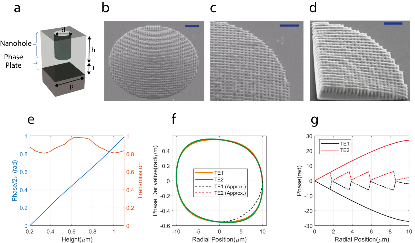
A 3D achromatic metalenses.
(a) The unit structure of the metalens merges a nanohole and a phase plate. The dimensions d, h, p and t represent diameter, height, and period of the nanoholes and thickness of the phase plate, respectively. We set d = 0.2 μm and p = 0.4 μm. (b) Scanning electron micrograph of 20 μm diameter metalens. The structure is fabricated with two-photon lithography on a fused silica substrate. Scale bar is 3 μm. (c) Zoomed-in image of 20 μm diameter metalens. The holes are clearly visible on the surface. (d) Quarter-section of 20 μm diameter metalens showing the varying hole depth. Scale bar is 2 μm. (e) Phase shift and transmission of nanoholes as the function of depth at 450 nm wavelength. (f, g) Phase derivative and the phase shift distribution as the function of radial coordinates for EPD = 20 μm and NA = 0.27 achromatic metalens.
The two TEs, the phase plate (bottom) and nanoholes (top), are merged into a single structure which forms the unit cell of the hybrid metalens as shown in Figure 1(a). The nanohole structure is chosen due to its higher transmission than the nanopillar [29] and advantages for fabrication. Specifically, the nanohole architecture prevents pattern distortion and collapse that can accompany high aspect ratio pillars. Figure 1(d) shows the phase shift library as the function of depth of the nanoholes under the assumption of locally periodic structure [30]. We limit the depth of the nanoholes to 0.8 μm because of fabrication constraints. The remaining phase shift is achieved by the phase plate structure.
The phase shift through a phase plate is expressed by the well-known formula
3 Experimental results
To test our designs, we fabricated two different lenses having EPD = 20, 200 µm and NA = 0.27, 0.04, respectively. The lenses were fabricated on 0.7 mm thick fused-silica substrates using “dip-in” multi-photon lithography. Multi-photon lithography exploits two-photon crosslinking in the focal volume of an ultrafast laser pulse to create true 3D structures in a single process step [31], [32]. Fabricated metalenses are shown Figure 1b, c. Lenses were characterized using a collimated beam from a supercontinuum source.
Figure 2a illustrates measured power intensity distributions in y–z plane and intensity distribution at the focal plane. Figure 2b compares normalized power intensity profiles at the focal plane and the diffraction-limited Airy disk pattern. We define the focal plane as the z-coordinate of the maximum measured power intensity on top of the metalens. The measured focusing efficiency as a function of wavelength is shown in Figure 2c. Focusing efficiency is defined as the ratio of integrated power within the circle having radius 1.5 × FWHM to the incident power on the metalens. The average efficiency values are 60 and 42% for 20 and 100 μm lenses, respectively. Comparison of measured and diffraction-limited full-width at half-maximum (FWHM) at the focal plane is also provided in Figure 2d. Diffraction limited performance is clear from the plot. The focusing error versus wavelength is shown in Figure 2e. We define the focusing error as the normalized difference between the nominal and the measured focal length. The maximum deviation from the mean focal length is measured as 6% showing that the metalens has effectively corrected chromatic aberration over the entire visible to short-wave IR bandwidth.
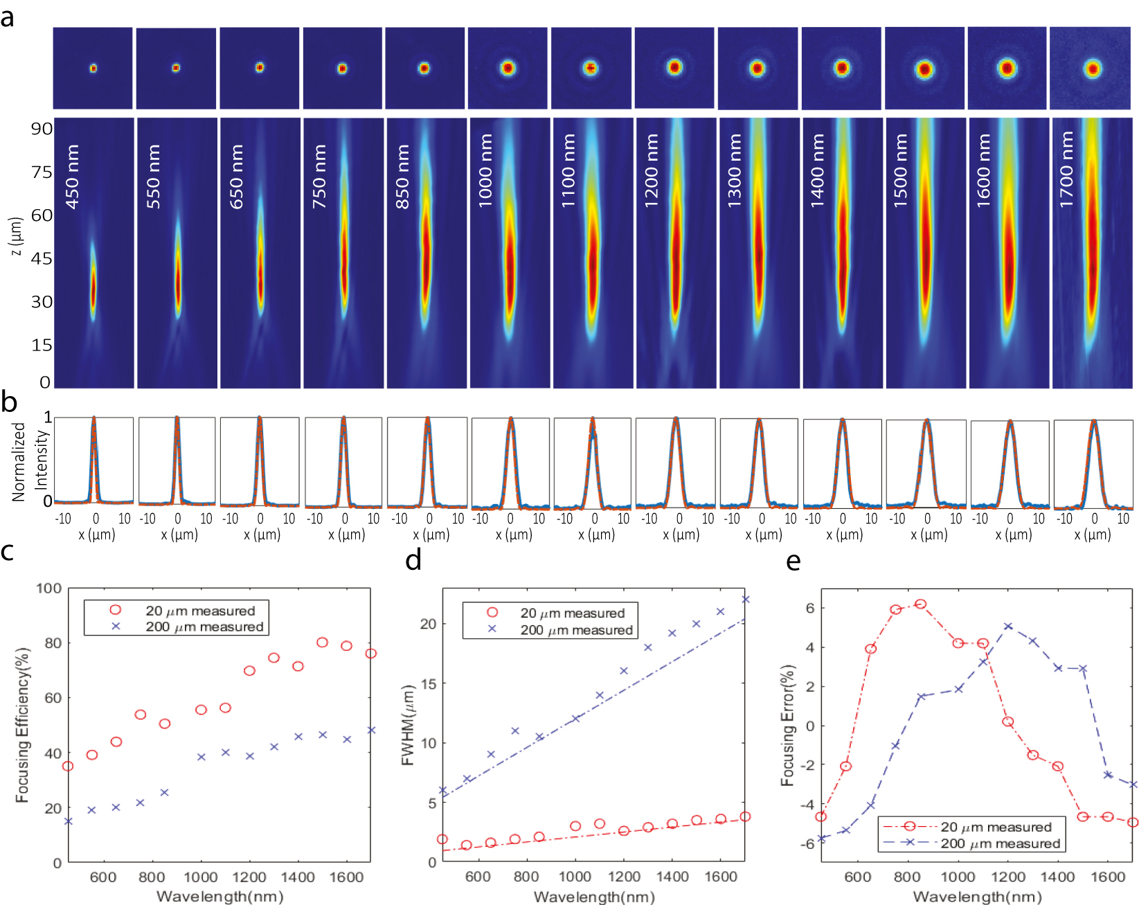
Experimentally measured performance of the metalens.
(a) Power intensity distribution in the x–y focal plane (upper) and x–z (lower) planes. Maximum power intensity appears around the focal plane at z ≈ 36 μm. (b) Comparison of diffraction-limited Airy function (dashed red lines) and the measured power intensity across the focal plane (solid blue curve). We normalize the Airy fit so that the maximum intensity is unity. (c) Measured focusing efficiency as a function of wavelength. (d) Comparison of measured full-width at half-maximum (FWHM) with the diffraction limit. Dashed lines represent diffraction-limited performance. (e) Focal length error versus wavelength. Corresponding focal plane distances are 36 and 2600 μm for the 20 and 200 μm aperture size lenses, respectively.
We tested the imaging performance of EPD = 200 μm and NA = 0.04 metalens using the standard 1951 United States Air Force (USAF) target. Details of the experiment are explained in the supplementary information. Figure 3a shows the imaging results for group 5 (where 5–4 represents 45.3 line pairs/mm). Achromatic performance can be seen from the images taken under broadband (450–1700 nm) and SWIR (1000–1700 nm) illumination. We use a long-pass filter for the second image where wavelengths shorter than 1000 nm are filtered out. Practical usage of the metalens over the entire bandwidth is revealed by the Lego image in Figure 3(b). The SWIR and visible wavelength regimes were also separately tested as shown in Figure 3c–f.
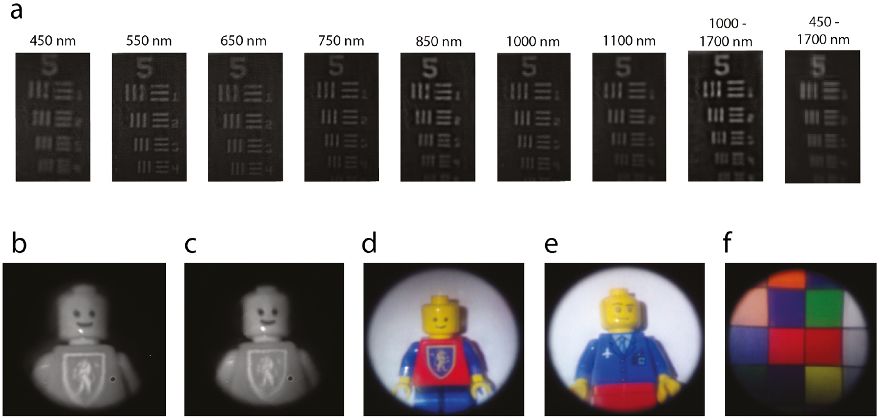
Imaging with EPD = 200 μm, NA = 0.04 metalens under halogen lamp illumination.
(a) Standard USAF target images for several wavelengths. (b, c) Images taken under illumination with wavelength ranges 450–1700 nm and 1000–1700, respectively. (d–f) Images taken by a color camera sensitive to visible spectrum.
4 Discussion and conclusion
Despite this excellent overall performance, we observe a reduction in focusing efficiency as the wavelength moves from the SWIR to the visible regime. The metalens’ period plays a major role in maximizing the efficiency and transmission; as a result, higher efficiency may be obtained from similar designs employing finer periods. Shorter wavelengths are also more sensitive to fabrication imperfections, which may account for some additional reduction in performance. Further advances in two-photon lithography or a transition to gray-scale e-beam lithography may alleviate this while preserving the metalens’ 3D geometry.
Regardless, nanohole structures proved to have distinct advantages compared to nanopillars. First, nanoholes offer higher transmission as expected [29]. Equally important, nanoholes reduced fabrication difficulties making subwavelength structures with higher aspect ratios accessible for operation with visible light. Finally, the nanohole-phase plate geometry should be replicable by molding for mass production. Thus, 3D metalenses based on nanoholes are excellent candidates when achromatic diffraction-limited focusing and imaging is required over the entire visible to short-wave IR spectrum.
Funding source: Intel Corporation
Funding source: National Science Foundation
Award Identifier / Grant number: ECCS-2025075, CMMI-1125998
Author contributions: All the authors have accepted responsibility for the entire content of this submitted manuscript and approved submission.
Research funding: This work was partially supported by Intel Corp. The authors thank the UK Center for Nanoscale Science and Engineering, a member of the National Nanotechnology Coordinated Infrastructure (NNCI), which is supported by the National Science Foundation (ECCS-2025075). This work used equipment supported by National Science Foundation Grant No. CMMI-1125998.
Conflict of interest statement: The authors declare no conflicts of interest regarding this article.
References
[1] S. Jahani and Z. Jacob, “All-dielectric metamaterials,” Nat. Nanotechnol., vol. 11, p. 23, 2016, https://doi.org/10.1038/nnano.2015.304.Search in Google Scholar PubMed
[2] N. Yu and F. Capasso, “Flat optics with designer metasurfaces,” Nat. Mater., vol. 13, p. 139, 2014, https://doi.org/10.1038/nmat3839.Search in Google Scholar PubMed
[3] P. Lalanne and P. Chavel, “Metalenses at visible wavelengths: Past, present, perspectives,” Laser Photonics Rev., vol. 11, p. 1600295, 2017, https://doi.org/10.1002/lpor.201600295.Search in Google Scholar
[4] N. Yu, P. Genevet, M. A. Kats, et al., “Light propagation with phase discontinuities: Generalized laws of reflection and refraction,” Science, vol. 334, p. 333, 2011, https://doi.org/10.1126/science.1210713.Search in Google Scholar PubMed
[5] H.-T. Chen, A. J. Taylor, and N. Yu, “A review of metasurfaces: Physics and applications,” Rep. Prog. Phys., vol. 79, p. 076401, 2016, https://doi.org/10.1088/0034-4885/79/7/076401.Search in Google Scholar PubMed
[6] F. Balli, M. A. Sultan, and J. T. Hastings, “Rotationally tunable polarization-insensitive metasurfaces for generating vortex beams,” in Metamaterials, Metadevices, and Metasystems 2020, SPIE, p. 11460, 2020.10.1117/12.2567798Search in Google Scholar
[7] M. Khorasaninejad, W. T. Chen, R. C. Devlin, J. Oh, A. Y. Zhu, and F. Capasso, “Metalenses at visible wavelengths: Diffraction-limited focusing and subwavelength resolution imaging,” Science, vol. 352, p. 1190, 2016.10.1126/science.aaf6644Search in Google Scholar PubMed
[8] N. Meinzer, W. L. Barnes, and I. R. Hooper, “Plasmonic meta-atoms and metasurfaces,” Nat. Photonics, vol. 8, p. 889, 2014, https://doi.org/10.1038/nphoton.2014.247.Search in Google Scholar
[9] E. Arbabi, A. Arbabi, S. M. Kamali, Y. Horie, and A. Faraon, “Multiwavelength metasurfaces through spatial multiplexing,” Sci. Rep., vol. 6, p. 32803, 2016, https://doi.org/10.1038/srep32803.Search in Google Scholar PubMed PubMed Central
[10] M. Khorasaninejad, A. Y. Zhu, C. Roques-Carmes, et al., “Polarization-insensitive metalenses at visible wavelengths,” Nano Lett., vol. 16, p. 7229, 2016, https://doi.org/10.1021/acs.nanolett.6b03626.Search in Google Scholar PubMed
[11] A. Arbabi, Y. Horie, M. Bagheri, and A. Faraon, “Dielectric metasurfaces for complete control of phase and polarization with subwavelength spatial resolution and high transmission,” Nat. Nanotechnol., vol. 10, p. 937, 2015, https://doi.org/10.1038/nnano.2015.186.Search in Google Scholar PubMed
[12] A. Arbabi, E. Arbabi, S. M. Kamali, Y. Horie, S. Han, and A. Faraon, “Miniature optical planar camera based on a wide-angle metasurface doublet corrected for monochromatic aberrations,” Nat. Commun., vol. 7, p. 13682, 2016, https://doi.org/10.1038/ncomms13682.Search in Google Scholar PubMed PubMed Central
[13] A. Özdemir, Z. Hayran, Y. Takashima, and H. Kurt, “Polarization independent high transmission large numerical aperture laser beam focusing and deflection by dielectric Huygens’ metasurfaces,” Optic Commun., vol. 401, p. 46, 2017, https://doi.org/10.1016/j.optcom.2017.05.031.Search in Google Scholar
[14] B. Groever, W. T. Chen, and F. Capasso, “Meta-lens doublet in the visible region,” Nano Lett., vol. 17, p. 4902, 2017, https://doi.org/10.1021/acs.nanolett.7b01888.Search in Google Scholar PubMed
[15] M. Khorasaninejad, Z. Shi, A. Y. Zhu, et al., “Achromatic metalens over 60 nm bandwidth in the visible and metalens with reverse chromatic dispersion,” Nano Lett., vol. 17, p. 1819, 2017, https://doi.org/10.1021/acs.nanolett.6b05137.Search in Google Scholar PubMed
[16] S. Shrestha, A. C. Overvig, M. Lu, A. Stein, and N. Yu, “Broadband achromatic dielectric metalenses,” Light Sci. Appl., vol. 7, p. 85, 2018, https://doi.org/10.1038/s41377-018-0078-x.Search in Google Scholar PubMed PubMed Central
[17] W. T. Chen, A. Y. Zhu, V. Sanjeev, et al., “A broadband achromatic metalens for focusing and imaging in the visible,” Nat. Nanotechnol., vol. 13, p. 220, 2018, https://doi.org/10.1038/s41565-017-0034-6.Search in Google Scholar PubMed
[18] W. T. Chen, A. Y. Zhu, J. Sisler, Z. Bharwani, and F. Capasso, “A broadband achromatic polarization-insensitive metalens consisting of anisotropic nanostructures,” Nat. Commun., vol. 10, p. 355, 2019, https://doi.org/10.1038/s41467-019-08305-y.Search in Google Scholar PubMed PubMed Central
[19] S. Wang, P. C. Wu, V.-C. Su, et al., “Broadband achromatic optical metasurface devices,” Nat. Commun., vol. 8, p. 187, 2017, https://doi.org/10.1038/s41467-017-00131-4.Search in Google Scholar PubMed PubMed Central
[20] S. Wang, P. C. Wu, V.-C. Su, et al., “A broadband achromatic metalens in the visible,” Nat. Nanotechnol., vol. 13, p. 227, 2018.10.1038/s41565-017-0052-4Search in Google Scholar PubMed
[21] S. Colburn, A. Zhan, and A. Majumdar, “Metasurface optics for full-color computational imaging,” Sci. Adv., vol. 4, p. eaar2114, 2018, https://doi.org/10.1126/sciadv.aar2114.Search in Google Scholar PubMed PubMed Central
[22] M. Khorasaninejad, F. Aieta, P. Kanhaiya, et al., “Achromatic metasurface lens at telecommunication wavelengths,” Nano Lett., vol. 15, p. 5358, 2015, https://doi.org/10.1021/acs.nanolett.5b01727.Search in Google Scholar PubMed
[23] F. Presutti and F. Monticone, “Focusing on bandwidth: Achromatic metalens limits,” Optica, vol. 7, p. 624, 2020, https://doi.org/10.1364/optica.389404.Search in Google Scholar
[24] A. Ndao, L. Hsu, J. Ha, J.-H. Park, C. Chang-Hasnain, and B. Kanté, “Octave bandwidth photonic fishnet-achromatic-metalens,” Nat. Commun., vol. 11, pp. 1–6, 2020, https://doi.org/10.1038/s41467-020-17015-9.Search in Google Scholar PubMed PubMed Central
[25] F. Balli, M. Sultan, S. K. Lami, and J. T. Hastings, “A hybrid achromatic metalens,” Nat. Commun., vol. 11, p. 1, 2020, https://doi.org/10.1038/s41467-020-17646-y.Search in Google Scholar PubMed PubMed Central
[26] M. A. Sultan, F. Balli, D. L. Lau, and J. Hastings, “Hybrid metasurfaces for simultaneous focusing and filtering,” Optic Lett., vol. 46, p. 214, 2020.10.1364/OL.410080Search in Google Scholar PubMed
[27] M. W. Farn and J. W. Goodman, “Diffractive doublet corrected on-axis at two wavelengths,” in 1990 Intl Lens Design Conf, G. N. Lawrence, Ed., Monterey, United States, 1991, p. 24.10.1117/12.47890Search in Google Scholar
[28] M. W. Farn and J. W. Goodman, “Diffractive doublets corrected at two wavelengths,” J. Opt. Soc., vol. 8, p. 860, 1991, https://doi.org/10.1364/josaa.8.000860.Search in Google Scholar
[29] N. Yilmaz, A. Ozer, A. Ozdemir, and H. Kurt, “Nanohole-based phase gradient metasurfaces for light manipulation,” J. Phys. Appl. Phys., vol. 52, p. 205102, 2019, https://doi.org/10.1088/1361-6463/ab0c70.Search in Google Scholar
[30] R. Pestourie, C. Pérez-Arancibia, Z. Lin, W. Shin, F. Capasso, and S. G. Johnson, “Inverse design of large-area metasurfaces,” Optic Express, vol. 26, p. 33732, 2018, https://doi.org/10.1364/oe.26.033732.Search in Google Scholar
[31] S. Maruo, O. Nakamura, and S. Kawata, “Three-dimensional microfabrication with two-photon-absorbed photopolymerization,” Optic Lett., vol. 22, p. 132, 1997, https://doi.org/10.1364/ol.22.000132.Search in Google Scholar PubMed
[32] G. von Freymann, A. Ledermann, M. Thiel, et al., “Three-dimensional nanostructures for photonics,” Adv. Funct. Mater., vol. 20, p. 1038, 2010, https://doi.org/10.1002/adfm.200901838.Search in Google Scholar
Supplementary Material
The online version of this article offers supplementary material (https://doi.org/10.1515/nanoph-2020-0550).
© 2021 Fatih Balli et al., published by De Gruyter, Berlin/Boston
This work is licensed under the Creative Commons Attribution 4.0 International License.
Articles in the same Issue
- Reviews
- Raman scattering in high-refractive-index nanostructures
- Polymerization mechanisms initiated by spatio-temporally confined light
- THz spintronic emitters: a review on achievements and future challenges
- Research Articles
- An ultrabroadband 3D achromatic metalens
- Silicon integrated multi-mode ring resonator
- Formation of laser-induced periodic surface nanometric concentric ring structures on silicon surfaces through single-spot irradiation with orthogonally polarized femtosecond laser double-pulse sequences
- Integrated and spectrally selective thermal emitters enabled by layered metamaterials
- Ultrasensitive terahertz sensing with high-Q toroidal dipole resonance governed by bound states in the continuum in all-dielectric metasurface
- Electrically injected parity-time symmetric distributed feedback laser diodes (DFB) for telecom applications
- Injection locking in an optomechanical coherent phonon source
- Plasmon extinguishment by bandedge shift identified as a second-order spectroscopic differentiation
- Dual functionality metamaterial enables ultra-compact, highly sensitive uncooled infrared sensor
- All-dielectric chiral coding metasurface based on spin-decoupling in terahertz band
- Parity-time symmetry and coherent perfect absorption in a cooperative atom response