NanoLEDs for energy-efficient and gigahertz-speed spike-based sub-λ neuromorphic nanophotonic computing
-
Bruno Romeira

 ,
José M. L. Figueiredo
,
José M. L. Figueiredo

Abstract
Event-activated biological-inspired subwavelength (sub-λ) photonic neural networks are of key importance for future energy-efficient and high-bandwidth artificial intelligence systems. However, a miniaturized light-emitting nanosource for spike-based operation of interest for neuromorphic optical computing is still lacking. In this work, we propose and theoretically analyze a novel nanoscale nanophotonic neuron circuit. It is formed by a quantum resonant tunneling (QRT) nanostructure monolithic integrated into a sub-λ metal-cavity nanolight-emitting diode (nanoLED). The resulting optical nanosource displays a negative differential conductance which controls the all-or-nothing optical spiking response of the nanoLED. Here we demonstrate efficient activation of the spiking response via high-speed nonlinear electrical modulation of the nanoLED. A model that combines the dynamical equations of the circuit which considers the nonlinear voltage-controlled current characteristic, and rate equations that takes into account the Purcell enhancement of the spontaneous emission, is used to provide a theoretical framework to investigate the optical spiking dynamic properties of the neuromorphic nanoLED. We show inhibitory- and excitatory-like optical spikes at multi-gigahertz speeds can be achieved upon receiving exceptionally low (sub-10 mV) synaptic-like electrical activation signals, lower than biological voltages of 100 mV, and with remarkably low energy consumption, in the range of 10–100 fJ per emitted spike. Importantly, the energy per spike is roughly constant and almost independent of the incoming modulating frequency signal, which is markedly different from conventional current modulation schemes. This method of spike generation in neuromorphic nanoLED devices paves the way for sub-λ incoherent neural elements for fast and efficient asynchronous neural computation in photonic spiking neural networks.
1 Introduction
Artificial intelligence (AI) systems using computing algorithms of deep learning neural networks (DNNs) are emerging rapidly [1]. Despite the truly remarkable achievements of algorithms of neural networks executing intelligent, human-like, tasks such as pattern recognition and decision-making (e. g. AlphaGo [2]), the power budget involved in running these DNNs in standard von Neumann computers is growing exponentially [3]. Instead, the human brain is more than five orders of magnitude more efficient than all current DNNs [4], [5]. The key difference relies in the vast connectivity of the brain that takes advantage of a unique sparse and extremely efficient information transfer via the action potentials in neurons – known as “nerve impulses” or “spikes”.
Currently, AI systems rely on three main generations of neural networks based on their neuronal functionality [6]: i) the McCullock-Pitt perceptron which performs thresholding operation resulting in a digital output; ii) DNN which adds continuous nonlinearity to the neuronal unit enabling to have multiple hidden layers between input and output; and iii) spiking neural network (SNN) that uses neuronal units that exchange information via spikes. SNNs use the timing of the spikes (binary events) to process information whereas the neuronal unit is only active when receiving or emitting spikes. This reduces substantially the energy over a given period of time. It is estimated that in the brain a consumption of only ∼104 adenosine triphosphate (ATP) molecules is needed to transmit a spike (bit) at a chemical synapse [7], equivalent to ∼1 fJ/bit at 32 bit/s.
Neuromorphic hardware elements for spiking emulation have been addressed using electronics (e. g., TrueNorth using complementary metal-oxide-semiconductors [8]) but typically operate at low speeds (∼kHz) and consume several pJ/spike. For low energy, sub-pJ/spike, synaptic-like functionalities, non-volatile materials such as resistive random-access memory, phase-change memory and spin-transfer torque magnetic random-access-memory offer alternatives to silicon (see [9], [10] and [11] for a comprehensive review). Despite the remarkable progresses, fan-out and parasitic constraints of electronic approaches limit the power budget for scalable solutions.
In the context of photonics, demonstrations of optical neural networks using coherent light-based DNN accelerators [12], [13] and reservoir computing [14], [15], take advantage of the high bandwidth-distance products, lower electromagnetic interference and lower power consumption of optical interconnects [16]. Although these architectures do not use spike-based learning they are capable of remarkable light-based, human-like, recognition tasks under supervised learning [15]. In order reproduce the powerful computation of biological neurons at lower energy cost there has been numerous implementations of spike-based photonic neurons using graphene excitable lasers [17], distributed feedback (DFB) lasers [18], vertical-cavity surface-emitting lasers (VCSEL) [19], [20], time-delayed optoelectronic nanoscale resonators [21], micropillar lasers [22], or phase change materials [23] to name a few (for an extensive review see [24]). Nevertheless, the large footprint (>100 μm2) of most of these elements is imposing a bottleneck for compact and efficient optical SNNs. A key driver for scalable SNNs is aggressive scaling-down of existing photonic elements, specifically the optical source, to the sub-μm scale for efficient (<10 fJ/spike), fast (>10 GHz) and miniaturized solutions. However, the development of such a subwavelength-scale (sub-λ) light source, well-matched for brain-like photonic spike-based computing, remains a challenge.
In order to reduce the size of a light source well below the micrometer scale, a plethora of nanolasers have been proposed in the last 15 years using photonic crystal cavities [25], [26], [27], metallic-cavity cavities [28] and plasmonic cavities [29] (for an extensive review see [30], [31]), but the unlocking of their potential for neuromorphic computing remains unexplored. However, for short distance intra-chip interconnections and brain-like asynchronous neural computation, lasing is not a main requirement turning incoherent nanolight-emitting diode (nanoLED) sources as excellent alternatives to nanolasers. Differently from nanolasers, nanoLEDs do not require a lasing threshold and therefore do not need a high-Q cavity, resulting in much lower current operation requirements [32]. Importantly, in recent years several advances have been made to increase the efficiency of nanoLEDs towards >10% which include Purcell enhancement of radiative emission [33], [34], [35], suppression of nonradiative surface effects via chemical passivation treatments [36], and efficient waveguide-coupling methods [37], [38]. NanoLEDs have been already demonstrated for a photonic crystal (PhC) LED [39], a plasmonic LED [40] and a waveguide-coupled nanoLED [37], showing output power levels in the order of tens to hundreds of pW for the PhC case and up to 300 nW for the waveguide-coupled case. Nonetheless, all these reported LEDs are “linear” devices not featuring non-linear spiking-like activation in the form of short pulses, which is crucial to reproduce the biological neural dynamics, as already shown for the case of optically pumped microlasers [22]. To overcome this, a circuit using a neuron-like superconducting-nanowire single-photon detector driving an LED has been proposed for cryogenic neuromorphic computing [41]. However, the low-temperature requirements and slow speed (∼MHz) limited by the spontaneous emission rate (∼ns), limits this approach for efficient, high-speed and compact solutions.
In this work, we propose and theoretically analyze a novel sub-λ nanophotonic spiking neuron circuit. It is based on a metal-cavity neuromorphic nanoLED for event-driven neural computation. The semiconductor epitaxial heterostructure of our neuron-like unit is formed by a quantum resonant tunneling (QRT) nanostructure monolithic integrated in a double heterostructure LED. The QRT enables control of the injection of electrons into the active region of the LED. This provides an intensity modulated nanoLED with a voltage-controlled negative differential conductance (NDC). The activation of the all-or-nothing optical spiking response (called excitable) is achieved via high-speed nonlinear electrical modulation of the nanoLED. Importantly, the sub-λ metal-cavity offers strong light–matter interaction at the nanoscale via the Purcell effect [30], which scales inversely with the mode volume [31], [38], leading to faster and more efficient light emission and of advantage for high-bandwidth optical spiking. Using a model that combines the dynamical equations of the circuit and rate equations, and using realistic parameters of a nanodevice that takes into account material parameters, nonradiative effects and size scaling, we analyze the characteristics of the fired optical spikes. We conclude that for optical nanosources with ∼0.01 μm2 mode volume, intensity modulated optical spiking with sub-nanosecond refractory time responses can be achieved upon receiving exceptionally low (sub-10 mV) incoming synaptic-like activation signals, close to the shot-noise limit. This is lower than the amplitude of 100 mV in biological counterparts and much smaller than the typical switching voltages (0.2–2 V) of memristive devices [42]. Notably, we conclude the optical energy per spike is roughly constant and therefore, at some extent, almost independent of the incoming modulating frequency signal, a situation markedly different from standard current modulation methods of light sources [31], [37], [43]. This provides a new modulation scheme in nanoLEDs featuring all the key requirements of spike-based sub-λ neuromorphic optical computing.
2 Key ingredients of neuromorphic nanoLEDs
2.1 Low-dimensional quantum resonant tunneling (QRT) nanostructures
Semiconductor QRT nanostructures use a single or multiple double barrier quantum well (DBQW) of around 10 nm thick in the epitaxial growth direction for 1D carrier confinement and filtering [44]. The energy passband-like filtering leads to a current-voltage (I-V) characteristic displaying a region of NDC that persists at room-temperature from direct current (DC) up to terahertz [44]. These structures when employing a single DBQW are widely known as resonant tunneling diodes (RTDs), and can have cut-off frequencies up to 1.9 THz [45]. Remarkably, the theoretical cut-off frequency of single DBQW-QRTs is limited by the tunneling escape time in the quantum well [44]. As a result, the quantum resonant tunneling effect and NDC characteristic has been exploited in a wide-range of electronic and photonic devices, including THz quantum cascade lasers for gas sensing [46], THz emitters and detectors for imaging [47], and communications beyond 5G (world record oscillation at 1.92 THz [45]), single-photon switches and detectors [48], [49], electroluminescence in III-nitride LED sources [50], III-V unipolar bistable QRT [51], bipolar QRT-based LEDs [52], [53], [54] and lasers [55], [56], near-IR photodetectors for optical communications [57], and mid-IR detectors for sensing [58], to name only a few.
For neuron computation, early works evoked QRT-based devices as potential nanoelectronic candidates for cellular neural networks as a form of threshold logical gates [59]. In the context of photonics, early works on n-type (unipolar) QRT nanostructures integrated with highly photo-sensitive absorption layers of interest for synaptic- and autaptic-like bio-neural functionalities have been exploited using either bistable or excitable regimes to enable stochastic resonance [60], spiking [61] or autaptic (self-feedback) neuron-like signaling [21]. Despite these works, the monolithic integration of QRT nanostructures in light-emitting configurations at the nanoscale for ultrafast and energy-efficient spike-based sub-λ neuromorphic functionalities remains unexplored.
2.2 Neuromorphic nanoLED device
The sub-λ nanophotonic spiking neuron unit proposed here is formed by a quantum resonant tunneling (QRT) nanostructure monolithic integrated in a double heterostructure LED, Figure 1A. The LED section consists of an inverted p-i-n AlGAs/GaAs/AlGaAs double heterostructure. The active region is made of GaAs for emission at ∼850 nm. Depending on the target emission, alternative active materials can be considered, namely quantum wells or quantum dots. The surrounded layers of AlGaAs (30% Al) with a lower refractive index are included for light confinement in the active region. The QRT section, crucial for the neuromorphic functionality, consists of a nanolayer formed by a lower band gap GaAs material, the well, sandwiched between two thinner layers of a larger bandgap AlAs material, the barriers. The QRT is monolithic integrated in the cathode (n-type region) section of the inverted p-i-n LED, Figure 1A. This minimizes the impact of the QRT on the LED optical performance, as previously considered in the monolithic integration of large area RTD-lasers [55], [56]. This is different from the situation where the QRT is embedded in the active region which shows poor performance at RT mainly attributed to the inefficient resonant tunneling hole injection and other hole current contributions [52], [53]. The QRT enables control of the injection of electrons into the active region of the LED. This provides a nanoLED with voltage-controlled NDC, red solid line in the top panel of Figure 1B, and is markedly different from the “linear” DC current-voltage characteristics of conventional LEDs (black dashed line). As a result, the all-or-nothing spiking (pulse-like) dynamic properties of neurons can be reproduced, with refractory time responses limited only by the circuit's RC constant, lower panel of Figure 1B, where R is the circuit resistance and C is the circuit capacitance. We note despite the small sizes considered here for the cross section of the nanodevices (∼200 nm), Figure 1C, one can still assume the energy of the QRT-based nanoLED is quantized only in the direction of the current flow, whereas other quantization effects due to the size of the structure in other directions will be negligible.
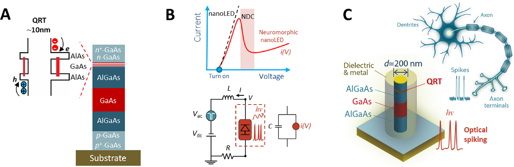
General description of the sub-λ nanophotonic neuron. A Schematic of the semiconductor epitaxial heterostructure (not to scale). It is formed by a QRT nanostructure monolithic integrated in a AlGaAs/GaAs/AlGaAs light-emitting diode epitaxial heterostrucuture. In the inset is shown the 10-nm thick QRT AlAs/GaAs/AlAs nanostructure in the n + n n + section. B (Top panel) Comparison of the I-V curves between a standard nanoLED (dashed line) and a neuromorphic nanoLED (solid red line). The neuromorphic nanoLED features an i(V) with a voltage-controlled NDC. (Lower panel) Schematic of the circuit. The diode is modeled by a nonlinear voltage-controlled current source, i(V), in parallel with the equivalent capacitance, C. The resistance, R, and inductance, L, are the equivalent lumped elements of the LED and electrical connections. The circuit includes a DC voltage source, Vdc, and a voltage time-dependent signal, Vac, for synaptic-like activation of the all-or-nothing spiking response. C Schematic of the sub-λ nanophotonic neuron in a 200 nm cross section nanopillar using a metal-dielectric configuration. Inset on top is shown the schematic representation of a biological neuron.
Lastly, to achieve a sub-λ nanophotonic neuron with dimensions approaching the sub-100 nm scale, Figure 1C, a nanopillar metallic cavity is considered. Although here we focus our analysis in metallic cavities we note that this configuration could be exploited, in principle, to other cavity configurations such as PhC or plasmonics. In the metal-cavity, the pillar is surrounded by a dielectric cap material (typically made of SiO2) and then coated with metal (usually Au or Ag). The metal-cavity envisioned for the neuromorphic nanoLED is similar to the one first reported for a waveguide-coupled nanoLED operating at room-temperature [37]. This enables LED devices with a small footprint and light confinement approaching the sub-100 nm scale. Crucial for the firing of fast spikes, the enhancement of the radiative emission in the cavity mode (also known as the Purcell effect [33]) allow us to potentially decrease the refractory time response of the optical spikes down to the 100 ps timescale. As will be discussed, the main challenges are related with the internal efficiency of the LEDs at room-temperature due to nonradiative effects. However, recent work suggests that sub-micrometer nanopillars can achieve exceptional large extraction efficiencies [62], which would strongly benefit the output power of these sources, even in the situation of unavoidable large nonradiative effects.
2.3 Theoretical model
Here, we describe the theoretical model to analyze the operation of the sub-λ neuromorphic nanoLED. It combines the dynamical equations of the circuit, Figure 1B (lower panel) and rate equations that takes into account the Purcell enhancement of the spontaneous emission. In particular, the rate equations model describing the nanoLED follows a similar formalism already introduced in [34]. However, differently from assuming a typical “linear” DC current input driving the LED, in our case the neuromorphic nanoLED is driven by an N-shape nonlinear voltage-controlled current,
The parameters that enter these equations are as follows. The parameter
where
The nanoLED’s rate equations for carrier number,
where
Assuming inhomogeneous broadening of the electronic states for a bulk emitter, the photon creation rate by spontaneous emission for homogeneously broadening two-level atom in a resonant cavity can be derived from the Fermi’s Golden rule [67]:
We note that Eq. (6) assumes that the emitter spectral width is broader than the single cavity mode spectral width for a cavity centered at the peak emission. This is typically the case for thermally broadened bulk active materials and has been recently extensively analyzed for both nanolasers and nanoLEDs [34], [67]. It is also the case of our neuromorphic nanoLED operating at room-temperature. In Eq. (6),
For simplicity of the numerical analysis, the total spontaneous emission in standard textbooks is often approximated by the bimolecular recombination coefficient,
For the nanoLEDS and range of parameters analyzed here the bimolecular recombination approximation describes reasonably well the expected static properties of the nanoLEDs predicted by a full model using
In what follows, departing from the dynamical equations of the circuit, (1), (2), the rate-equation model of the nanoLED, (7), (8), and the nonlinear voltage-controlled current source, (3), we examine the various scenarios of operation of neuromorphic micro- and nanoLEDs in terms of efficiency, speed limits and optical spiking dynamic properties and compare their performance with conventional current modulation schemes of micro- and nanoLED sources.
3 Static and spiking dynamics of neuromorphic nanoLEDs
3.1 Static nonlinear characteristics
In this section, our aim is to analyze the static characteristics of metal-cavity pillar-based LED structures, monolithic integrated with a QRT nanostructure, while considering realistic operation at room-temperature. We assume a practical device showing a representative I-V curve with similar features as the ones reported for a sub-μm nanocolumn resonant tunneling device (not considering the LED section) [70]. The I-V curve given by Eq. (3) is shown in Figure 2 and features a peak current of ∼100 μA, a peak-to-valley-current ratio (PVCR) ∼4 and an NDC region with a voltage range of about 50 mV. This I-V takes in to account the voltage turn-on of the inverted p-i-n junction of ∼1.5 V obtained from SILVACO simulations of the nanoLED portion of the full device [71]. We note that for the material system analyzed here, I-Vs with PVCRs up to six at room-temperature could be obtained using improved design of the DBQW structure [72].
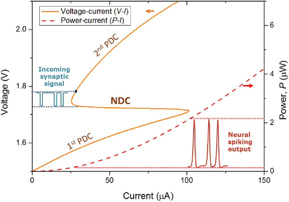
Light-current-voltage characteristics of the neuromorphic nanoLED showing the V-I nonlinear voltage-controlled current curve, i(V) (yellow solid trace), and the P-I curve (red-dashed trace). The i(V) with a region of NDC enables voltage induced on-off current switching upon an incoming synaptic-like signal resulting in an all-or-nothing neural spiking output in the optical domain.
For practical analysis and direct comparison we assume two representative neuromorphic LED structures with identical circuit parameters and I-V characteristics. The neuromorphic nanoLED is a disk metal-cavity nanopillar with a
For analysis the calculated photon number in (7), (8) is converted to an optical output power using:
where
Assuming the parameter values described previously, Figure 2 displays the calculated P-I curve for the nanoLED device. For current injection levels ∼75 μA it displays a power level ∼1 μW. In typical electrically current modulated LED sources this corresponds to an optical energy per bit close to 1 fJ at 1 Gb/s. We will use this value as a reference to compare the performance of our LED sources considering that in a practical application the detection of the emission from nanoLED sources requires thermal noise-limited receivers which typically require at least 1 fJ/bit.
Figure 3 displays the calculated P-V characteristics showing the optical power versus the injected voltage for the neuromorphic: A microLED and B nanoLED. The curves were simulated assuming a large value of surface recombination of
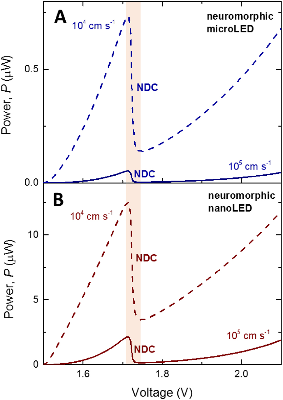
Simulated P-I nonlinear characteristics of the neuromorphic A microLED, and B nanoLED devices. In all curves, the solid lines correspond to a value of surface recombination 105 cm s−1 and the dashed lines to 104 cm s−1. The vertical shadow represents the NDC corresponding to the voltage region where the DC current decreases which leads to a pronounced N-shape characteristic of the emitted optical power.
In summary, sub-λ neuromorphic LED devices taking advantage of the radiative Purcell enhancement, combined with low surface passivation, can potentially operate at room-temperature with on-chip optical power levels >1 μW (corresponding to ∼5000 photons assuming gigahertz per second at the target wavelength), while showing large peak-to-valley-optical-power ratios of advantage for the neuromorphic optical spiking functionality.
3.2 Gigahertz-speed modulation bandwidth
Here, we analyze the modulation bandwidth results for the neuromorphic microLED and nanoLED devices as a function of the voltage-controlled current levels. We analyze the same voltage range as described previously for the case of the static nonlinear characteristics. To obtain the modulation bandwidth, we perform a small-signal analysis of Eqs. (7), (8) with a similar procedure as presented in [69], assuming as input the nonlinear voltage-controlled current curve given by Eq. (3). This allows us to calculate the 3-dB modulation frequency as a function of the voltage, Figure 4. As previously considered, here we investigate the effect of the surface recombination in the modulation speed of the devices. We have excluded from the small-signal analysis the region of NDC since it lies outside the steady-state DC points where other dynamical regimes can occur, namely oscillatory behavior.
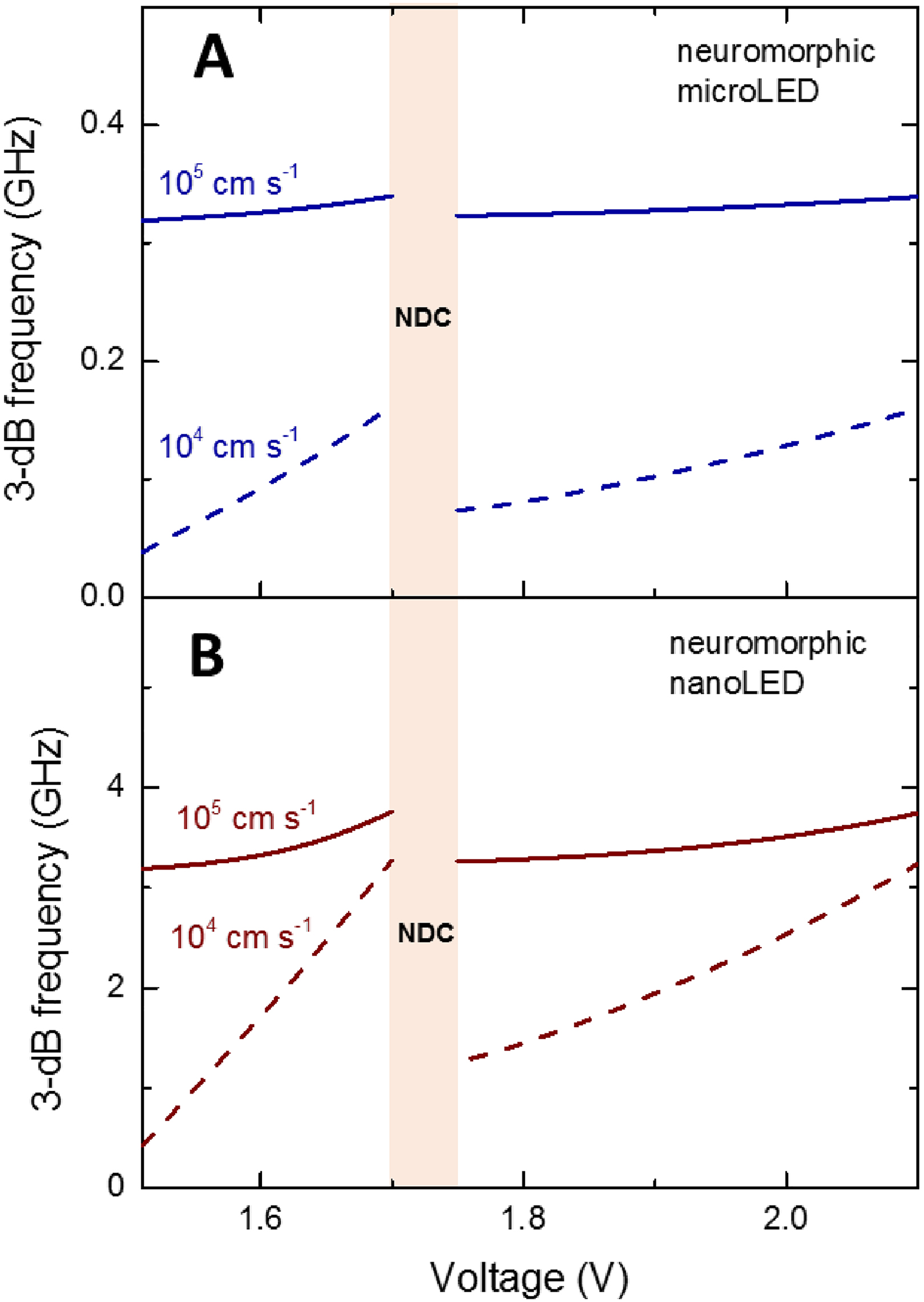
Simulated 3-dB bandwidth versus voltage for the neuromorphic A microLED, and B nanoLED devices. In all curves, the solid lines correspond to a surface recombination of 105 cm s−1 and the dashed lines to 104 cm s−1. The vertical shadow region represents the NDC corresponding to the voltage region where the DC current decreases.
The simulated curves of the small-signal 3-dB bandwidth versus voltage are shown in Figure 4. In the case of large surface recombination velocity values (solid lines) a maximum modulation bandwidth ∼0.34 GHz is achieved for the microLED when operating at the peak voltage ∼1.7 V, Figure 4A. In the voltage range analyzed here the modulation bandwidth does not change substantially from its maximum value, even at lower voltage (current) levels. In this case the effect of the surface recombination dominates over the radiative recombination rate. Effectively, this enables to operate the devices faster, even at low current injection levels. In the case of a low surface velocity of 104 cm s−1 a highly nonlinear 3-dB frequency plot (dashed curves) is obtained. This is as a result of the nonlinear I-V input which substantially modifies the current as a function of the applied voltage. In this case, the modulation bandwidth between the peak and valley is reduced from 150 to 70 MHz. This is a result of the reduction of the current injection and consequent lower radiative rate in the case of low surface recombination.
We now analyze the case of the nanoLED, Figure 4B. Assuming a large surface recombination (solid line) a 3-dB frequency of 3.75 GHz can be achieved at the peak voltage ∼1.7 V. Assuming the modulation bit rate is 1.3 the 3-dB small signal bandwidth, this corresponds to a modulation bandwidth close to 5 GHz. As described for the microLED, in the case of a low surface recombination (dashed curve) we obtain a highly nonlinear 3-dB frequency plot (dashed curves) due to the nonlinear I-V input. In this case, the modulation bandwidth at the peak voltage is ∼5 GHz while in the valley region the modulation bandwidth is ∼1.7 GHz. Effectively, neuromorphic nanoLEDs benefit from the Purcell enhancement of the radiative emission with potential to support multi-gigahertz speeds for optical spike modulation. For the nanoLED cases analyzed here, we note that in the peak region the 3-dB variation is not substantial for both low and high-surface recombination cases, while the emitted optical output is well above 1 µW in both scenarios, Figure 3B. Therefore, operating the neuromorphic nanoLEDs in the peak current (where nonradiative channels are already saturated) seems to provide a good compromise between emitted power and speed for both low and large surface recombination values, although as analyzed next the fired spikes would correspond to optical downward spikes.
3.3 Optical spiking dynamic properties
In what follows, departing from the dynamical equations of the circuit, (1), (2), the rate-equation model of the nanoLED, (7), (8), and the nonlinear voltage-controlled current source, (3), we examine the dynamic spike response of the nanoLED via high-speed nonlinear electrical activation. Here we focus our analysis on the activation response for the neuromorphic nanoLED case considering its potential to operate >1 GHz. For this purpose, we assume for the electrical circuit parameters of the nanoLED, lower panel of Figure 1B, an RC time constant of
For numerical analysis, we assume the best case scenario of a nanoLED with a low surface recombination and consider operation in a stationary quiescent point for the following DC bias: (a) vicinity of the valley voltage (V = 1.735 V), and (b) vicinity of the peak voltage (V = 1.722). In both situations, we assume a synaptic-like weak (sub-10 mV) external electrical stimulus, which forces the bias point out of stable equilibrium. Figure 5A shows the traces of the negative voltage pulses that activate optical upward spikes – excitatory-like signals – and Figure 5C shows the positive voltage pulses that activate optical downward spikes – the inhibitory-like signals. In both scenarios, the shortest incoming stimulus consists of a pulse width of 450 ps (panel (i)), i. e., larger than
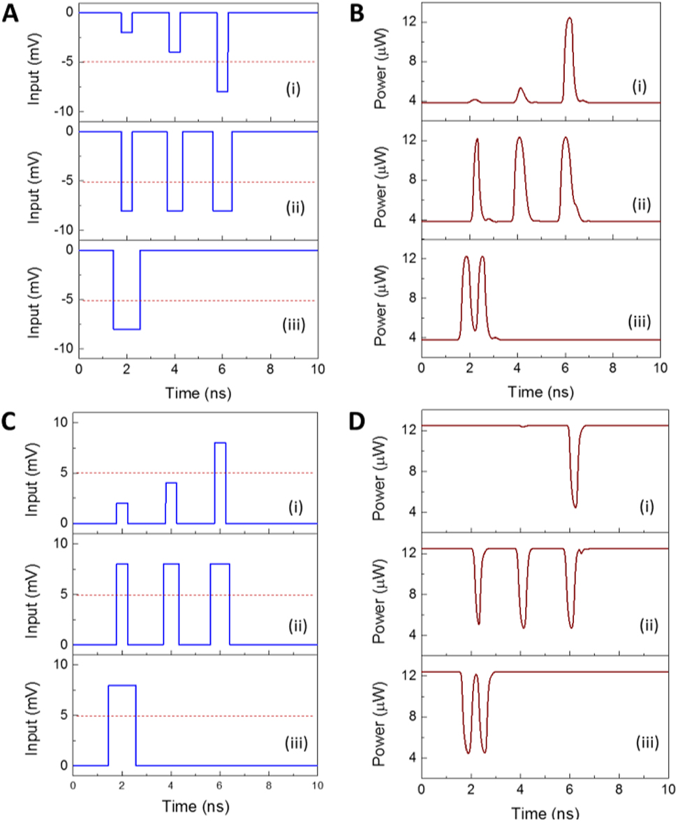
Optical spiking dynamic response of the neuromorphic nanoLED via high-speed nonlinear electrical (sub-10 mV) activation assuming a low surface recombination value. All-or-nothing excitatory (B) and inhibitory (D) optical spiking responses to incoming synaptic-like negative (A) and positive (B) voltage activation signals, respectively. The dashed red lines in A and C indicate the threshold level above which all-or-nothing spiking response is triggered.
In the scenario in the valley at V = 1.735 V, panel (i) of Figure 5 A and B, when the input remains below a threshold value, here at −5 mV (dashed red line), the output results in a weak linear response in current that is transformed into a similar quasi-linear optical output, see panel (i) of Figure 5B – this is similar to the standard case of an intensity modulated LED driven by current. When the negative voltage goes above the threshold value of −5 mV, the neuromorphic nanoLED fires a strongly nonlinear response consisting of an optical upward spike – the excitatory-like signal. This is a result of a valley-to-peak current switching induced by the voltage input. An opposite output is achieved in the scenario in the peak at V = 1.735 V, panel (i) of Figure 5C, D. Here the voltage input induces a peak-to-valley current switching resulting in an intensity modulated optical downward spike – the inhibitory-like signal.
We now analyze the remaining properties of the fired upward and downward optical spikes. Provided that the voltage is above the threshold value, the duration in time of the input pulse is less relevant for the characteristics of the output spike. This case is exemplified in panels ii) of Figure 5B, D for three incoming pulses (Figs. A and C) of 8 mV with a duration of 450 ps, 650 ps and 800 ps. Here, one can appreciate that a longer stimulation leads to an optical spike featuring similar amplitude and full width half maximum (FWHM) of ∼320 ps. Lastly, when the duration of the input pulse is larger than the so-called refractory time, multiple optical spikes can be fired. This scenario is displayed in panel iii) of Figure 5B, D showing two optical spikes fired with a time period corresponding to the lethargic time, here ∼650 ps. We notice that for realistic operation, the nanoLED excitable spiking response presented here uses incoming pulses of similar duration as the lethargic time of the neuromorphic nanoLED system. A more rigorous definition of all-or-nothing excitable response calls for employing triggering events that are typically much shorter than the lethargic time [77]. In this regard, it is important to mention that our system presents a type II scenario with Fitzhugh-Nagumo-like canard solutions, different from other optical systems, like for example an injected laser, which is a type I via a saddle-node on invariant circle scenario. Independently of the different dynamics involved, an obvious advantage of our neuromorphic nanoLEDs is that lasing is not needed to operate with such spiking responses.
In what follows, we summarize the operation of the neuromorphic nanoLED analyzed in Figure 5D in terms of electrical and optical energy per spike and compare with conventional current modulated (non-spiking) micro- and nanoLED sources. Figure 6 plots the electrical energy as a function of the optical energy per bit for received time duration of the bits ranging from 100 ns to 100 ps. The diagonal lines represent the operation of the LEDs in a non-spiking regime, that is, in a standard current modulation LED scenario operating in the vicinity of the valley voltage, here V = 1.735 V. The optical energy is calculated as
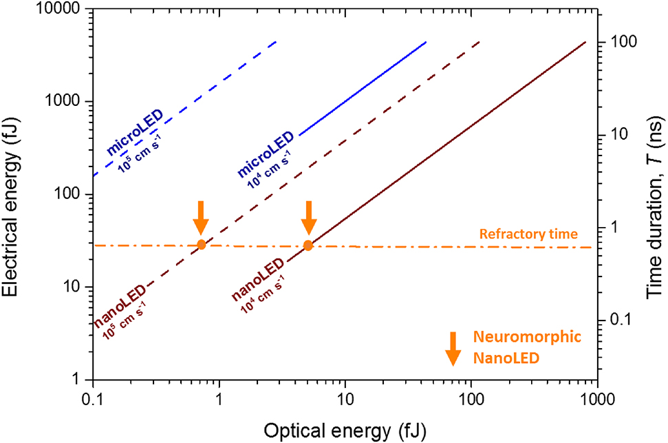
Electrical energy as a function of the optical energy per bit mapped for received time duration of the bits ranging from 100 ns to 100 ps. The diagonal lines are the values for the micro- and nanoLEDs in a non-spiking regime, that is, in a standard current modulation scenario assuming operation in the vicinity of the valley voltage at 1.735 V. The dashed lines represent the case of a large surface recombination of 105 cm s−1 while the solid lines represent the best case of a low surface recombination, 104 cm s−1. The dashed-dot horizontal line is the refractory time of the neuromorphic nanoLED, τref = 650 ps. The dashed-dot horizontal orange line intersecting the diagonal traces indicates the refractory time and gives the electrical/optical energy per spike (indicated by the vertical orange arrows) of the neuromorphic nanoLED assuming continuous firing of spikes and operation in the vicinity of the valley voltage.
We now analyze the operation of the neuromorphic nanoLED, also operating in the vicinity of the valley voltage. Assuming a scenario of continuous firing of optical spikes so that P is the average optical power output between the peak and valley points of the fired optical spikes, the performance of neuromorphic nanoLED in terms of electrical and optical energy per emitted spike operating in the spiking regime (indicated by the vertical orange arrows in Figure 6), is now set by the intersection between the dashed-dot horizontal orange line (corresponding to the refractory time,
In summary, we have analyzed the spiking response of our neuromorphic nanoLEDs via high-speed (sub-ns) nonlinear electrical modulation and have shown low energy consumption in the range of 10–100 fJ upon receiving small amplitude electrical synaptic signals of comparable voltages of biosystems. Although in this work we do not consider the case of incoming optical signals, our approach can potentially provide optically activated neuromorphic nanoLEDs using the photosensitive properties of resonant tunneling structures. Indeed, QRT-based photodetectors have been demonstrated [57], [78] exploiting that the tunneling current is extremely sensitive to changes in the local electrostatic potential, which enables highly-sensitive detection (104 A/W) of photogenerated minority charge carriers. Notably, the detection of low-level photons or even of single photons with enhanced quantum-efficiencies above η > 90 % can be potentially achieved by integration into photonic cavity structures [79], and this could be explored in future work using our nanocavity LED for fully optically interconnected artificial neurons.
4 Conclusion
In this work, we have analyzed a novel sub-λ nanophotonic spiking neuron circuit suited for spike-based neural computation. The proposed neuromorphic optical nanosource is formed by a quantum resonant tunneling (QRT) nanostructure monolithic integrated into a sub-λ metal-cavity nanoLED. The QRT is a key part of the device enabling control of the injection of electrons into the active region of the LED. This provides an intensity modulated nanoLED with a voltage-controlled negative differential conductance, well suited for all-or-nothing optical spiking modulation. We have examined the various scenarios of operation of two representative neuromorphic micro- and nanoLEDs with realistic operation at room-temperature in terms of efficiency, speed limits and optical spiking dynamic properties, and compared their performance with conventional current modulation schemes of LED sources. We demonstrated inhibitory- and excitatory-like optical spikes at multi-gigahertz speeds can be achieved upon receiving exceptionally low (sub-10 mV) synaptic-like electrical activation signals, lower than the amplitude of 100 mV in biological counterparts and much lower than the typical switching voltages of memristive devices, while providing remarkable low energy consumption, in the range of 10-100 fJ per emitted spike. Importantly, the energy per spike is roughly constant and almost independent of the incoming modulating frequency signal, which is noticeably different from conventional current modulation schemes of LED sources [37], [43]. Although our focus here has been in the analysis of the efficient activation of the optical spiking response via high-speed nonlinear electrical modulation of the nanoLED, this optical nanosource has the potential to enable optical activation of the all-or-nothing spiking response by taking advantage of the highly-sensitive photoresponse of the quantum resonant tunneling nanostructures [48], [57], [60]. Since our nanoLED cavities can be made much smaller than convention optical sources, in a practical application, the electrodes can be as small as the technology for electrical interconnecting to the CMOS chip or even more compact solutions using metal bonding directly to the metal-cavity nanoLEDs. This architecture and method of spike generation in neuromorphic nanoLED devices combined with techniques for more complex interconnectivity (e. g. nanowaveguides [37], or 3D interconnects [80]), paves the way for sub-λ incoherent spiking neural elements for optically interconnected photonic spiking neural networks and asynchronous neural computation.
Funding source: H2020 Future and Emerging Technologies
Award Identifier / Grant number: 828841
Acknowledgments
This work was supported in part by the European Commission through the H2020-FET-OPEN Project “ChipAI” under Grant Agreement 828841. The authors would like to thank Victor Dolores-Calzadilla, Meint Smit and Andrea Fiore, Eindhoven University of Technology, for fruitful discussions on the properties of metallo-dielectric nanoLEDs.
Author contribution: All the authors have accepted responsibility for the entire content of this submitted manuscript and approved submission.
Research funding: This work was supported in part by the European Commission through the H2020-FET-OPEN Project “ChipAI” under Grant Agreement 828841.
Employment or leadership: None declared.
Honorarium: None declared.
Conflict of interest statement: The authors declare no conflicts of interest regarding this article.
References
[1] Y. LeCun, Y. Bengio, and G. Hinton, “Deep learning,” Nature, vol. 521, no. 7553, pp. 436–444, 2015.10.1038/nature14539Suche in Google Scholar PubMed
[2] D. Silver, J. Schrittwieser, K. Simonyan, et al., “Mastering the game of go without human knowledge,” Nature, vol. 550, no. 7676, pp. 354–359, 2017.10.1038/nature24270Suche in Google Scholar PubMed
[3] X. Xu, Y. Ding, S. X. Hu, et al., “Scaling for edge inference of deep neural networks,” Nat. Electron., vol. 1, no. 4, pp. 216–222, 2018.10.1038/s41928-018-0059-3Suche in Google Scholar
[4] M. Fischetti, “Computers versus brains,” Scientific American, 2011, https://doi.org/10.1038/scientificamerican1111-104.10.1038/scientificamerican1111-104Suche in Google Scholar PubMed
[5] K. Meier, The Brain as Computer: Bad at Math, Good at Everything Else, Salem, MA, IEEE Spectrum, 2017.Suche in Google Scholar
[6] S. R. Nandakumar, S. R. Kulkarni, A. V Babu, and B. Rajendran, “Building brain-inspired computing systems: Examining the role of nanoscale devices,” IEEE Nanotechnol. Mag., vol. 12, no. 3, pp. 19–35, 2018.10.1109/MNANO.2018.2845078Suche in Google Scholar
[7] S. B. Laughlin, R. R. de Ruyter van Steveninck, and J. C. Anderson, “The metabolic cost of neural information,” Nat. Neurosci., vol. 1, no. 1, pp. 36–41, 1998. https://doi.org/10.1038/236.10.1038/236Suche in Google Scholar PubMed
[8] P. A. Merolla, J. V. Arthur, R. Alvarez-Icaza, et al., “A million spiking-neuron integrated circuit with a scalable communication network and interface,” Science, vol. 345, no. 6197, pp. 668–673, 2014.10.1126/science.1254642Suche in Google Scholar PubMed
[9] D. Ielmini and H.-S. P. Wong, “In-memory computing with resistive switching devices,” Nat. Electron., vol. 1, no. 6, pp. 333–343, 2018.10.1038/s41928-018-0092-2Suche in Google Scholar
[10] K. Roy, A. Jaiswal, and P. Panda, “Towards spike-based machine intelligence with neuromorphic computing,” Nature, vol. 575, no. 7784, pp. 607–617, 2019.10.1038/s41586-019-1677-2Suche in Google Scholar PubMed
[11] J. Zhu, T. Zhang, Y. Yang, and R. Huang, “A comprehensive review on emerging artificial neuromorphic devices,” Appl. Phys. Rev., vol. 7, no. 1, p. 11312, 2020.10.1063/1.5118217Suche in Google Scholar
[12] R. A. Heinz, J. O. Artman, and S. H. Lee, “Matrix multiplication by optical methods,” Appl. Opt., vol. 9, no. 9, pp. 2161–2168, Sep. 1970.10.1364/AO.9.002161Suche in Google Scholar PubMed
[13] Y. Shen, N. C. Harris, S. Skirlo, et al., “Deep learning with coherent nanophotonic circuits,” Nat. Photonics, vol. 11, no. 7, pp. 441–446, 2017, doi:https://doi.org/10.1038/nphoton.2017.93.10.1038/nphoton.2017.93Suche in Google Scholar
[14] D. Brunner, M. C. Soriano, C. R. Mirasso, and I. Fischer, “Parallel photonic information processing at gigabyte per second data rates using transient states,” Nat. Commun., vol. 4, no. 1, p. 1364, 2013.10.1038/ncomms2368Suche in Google Scholar PubMed PubMed Central
[15] P. Antonik, N. Marsal, D. Brunner, and D. Rontani, “Human action recognition with a large-scale brain-inspired photonic computer,” Nat. Mach. Intell., vol. 1, no. 11, pp. 530–537, 2019.10.1038/s42256-019-0110-8Suche in Google Scholar
[16] D. A. B. Miller, “Attojoule optoelectronics for low-energy information processing and communications,” J. Light. Technol., vol. 35, no. 3, pp. 346–396, Feb. 2017.10.1109/JLT.2017.2647779Suche in Google Scholar
[17] B. J. Shastri, M. A. Nahmias, A. N. Tait, A. W. Rodriguez, B. Wu, and P. R. Prucnal, “Spike processing with a graphene excitable laser,” Sci. Rep., vol. 6, no. 1, p. 19126, 2016.10.1038/srep19126Suche in Google Scholar PubMed PubMed Central
[18] H. Peng, G. Angelatos, T. F. de Lima, et al., “Temporal information processing with an integrated laser neuron,” IEEE J. Sel. Top. Quant. Electron., vol. 26, no. 1, pp. 1–9, 2020.10.1109/JSTQE.2019.2927582Suche in Google Scholar
[19] T. Deng, J. Robertson, Z. M. Wu, et al., “Stable propagation of inhibited spiking dynamics in vertical-cavity surface-emitting lasers for neuromorphic photonic networks,” IEEE Access, vol. 6, pp. 67951–67958, 2018.10.1109/ACCESS.2018.2878940Suche in Google Scholar
[20] M. A. Nahmias, B. J. Shastri, A. N. Tait, and P. R. Prucnal, “A leaky integrate-and-fire laser neuron for ultrafast cognitive computing,” IEEE J. Sel. Top. Quant. Electron., vol. 19, no. 5, pp. 1–12, 2013.10.1109/JSTQE.2013.2257700Suche in Google Scholar
[21] B. Romeira, R. Avo, J. M. L. Figueiredo, S. Barland, and J. Javaloyes, “Regenerative memory in time-delayed neuromorphic photonic resonators,” Sci. Rep., vol. 6, 2016, doi:https://doi.org/10.1038/srep19510.10.1038/srep19510Suche in Google Scholar PubMed PubMed Central
[22] F. Selmi, R. Braive, G. Beaudoin, et al., “Spike latency and response properties of an excitable micropillar laser,” Phys. Rev. E., vol. 94, no. 4, p. 42219, Oct. 2016.10.1103/PhysRevE.94.042219Suche in Google Scholar PubMed
[23] J. Feldmann, N. Youngblood, C. D. Wright, H. Bhaskaran, and W. H. P. Pernice, “All-optical spiking neurosynaptic networks with self-learning capabilities,” Nature, vol. 569, no. 7755, pp. 208–214, 2019.10.1038/s41586-019-1157-8Suche in Google Scholar PubMed PubMed Central
[24] P. R. Prucnal, B. J. Shastri, T. F. de Lima, M. A. Nahmias, and A. N. Tait, “Recent progress in semiconductor excitable lasers for photonic spike processing,” Adv. Opt. Photon., vol. 8, no. 2, pp. 228–299, Jun. 2016.10.1364/AOP.8.000228Suche in Google Scholar
[25] B. Ellis, M. Mayer, G. Shambat, et al., “Ultralow-threshold electrically pumped quantum-dot photonic-crystal nanocavity laser,” Nat. Photonics, vol. 5, p. 297, Apr. 2011.10.1038/nphoton.2011.51Suche in Google Scholar
[26] K. Takeda, T. Sato, A. Shinya, et al., “Few-fJ/bit data transmissions using directly modulated lambda-scale embedded active region photonic-crystal lasers,” Nat. Photonics, vol. 7, p. 569, May 2013.10.1038/nphoton.2013.110Suche in Google Scholar
[27] G. Crosnier, D. Sanchez, S. Bouchoule, et al., “Hybrid indium phosphide-on-silicon nanolaser diode,” Nat. Photonics, vol. 11, p. 297, Apr. 2017.10.1038/nphoton.2017.56Suche in Google Scholar
[28] M. T. Hill, Y. Oei, B. Smalbrugge, et al., “Lasing in metallic-coated nanocavities,” Nat. Photonics, vol. 1, p. 589, Sep. 2007.10.1038/nphoton.2007.171Suche in Google Scholar
[29] R. F. Oulton, V. Sorger, T. Zentgraf, et al., “Plasmon lasers at deep subwavelength scale,” Nature, vol. 461, p. 629, Aug. 2009.10.1038/nature08364Suche in Google Scholar PubMed
[30] R. M. Ma and R. F. Oulton, “Applications of nanolasers,” Nat. Nanotechnol., vol. 14, no. 1, pp. 12–22, 2019.10.1038/s41565-018-0320-ySuche in Google Scholar PubMed
[31] M. T. Hill and M. C. Gather, “Advances in small lasers,” Nat. Photonics, vol. 8, p. 908, Nov. 2014.10.1038/nphoton.2014.239Suche in Google Scholar
[32] K. L. Tsakmakidis, R. W. Boyd, E. Yablonovitch, and X. Zhang, “Large spontaneous-emission enhancements in metallic nanostructures: towards LEDs faster than lasers \[Invited\],” Opt. Express, vol. 24, no. 16, pp. 17916–17927, Aug. 2016.10.1364/OE.24.017916Suche in Google Scholar PubMed
[33] E. M. Purcell, “Spontaneous emission probabilities at radio frequencies,” Phys. Rev., vol. 69, no. 11, p. 681, 1946.10.1007/978-1-4615-1963-8_40Suche in Google Scholar
[34] B. Romeira and A. Fiore, “Physical limits of nanoleds and nanolasers for optical communications,” Proc. IEEE, pp. 1–14, 2019.10.1109/JPROC.2019.2912293Suche in Google Scholar
[35] M. S. Eggleston, K. Messer, L. Zhang, E. Yablonovitch, and M. C. Wu, “Optical antenna enhanced spontaneous emission,” Proc. Natl. Acad. Sci., vol. 112, no. 6, pp. 1704–1709, 2015.10.1073/pnas.1423294112Suche in Google Scholar PubMed PubMed Central
[36] A. Higuera-Rodriguez, B. Romeira, S. Birindelli, et al., “Ultralow surface recombination velocity in passivated InGaAs/InP nanopillars,” Nano Lett., vol. 17, no. 4, pp. 2627–2633, Apr. 2017.10.1021/acs.nanolett.7b00430Suche in Google Scholar PubMed PubMed Central
[37] V. Dolores-Calzadilla, B. Romeira, F. Pagliano, et al., “Waveguide-coupled nanopillar metal-cavity light-emitting diodes on silicon,” Nat. Commun., vol. 8, p. 14323, Feb. 2017.10.1038/ncomms14323Suche in Google Scholar PubMed PubMed Central
[38] M. S. Eggleston and M. C. Wu, “Efficient Coupling of an Antenna-Enhanced nanoLED into an Integrated InP Waveguide,” Nano Lett., vol. 15, no. 5, pp. 3329–3333, May 2015.10.1021/acs.nanolett.5b00574Suche in Google Scholar PubMed
[39] G. Shambat, B. Ellis, A. Majumdar, et al., “Ultrafast direct modulation of a single-mode photonic crystal nanocavity light-emitting diode,” Nat. Commun., vol. 2, p. 539, Nov 2011.10.1364/CLEO_SI.2012.CF1M.4Suche in Google Scholar
[40] K. C. Y. Huang, M.-K. Seo, T. Sarmiento, Y. Huo, J. S. Harris, and M. L. Brongersma, “Electrically driven subwavelength optical nanocircuits,” Nat. Photonics, vol. 8, p. 244, Feb. 2014.10.1038/nphoton.2014.2Suche in Google Scholar
[41] J. M. Shainline, S. M. Buckley, R. P. Mirin, and S. W. Nam, “Superconducting optoelectronic circuits for neuromorphic computing,” Phys. Rev. Appl., vol. 7, no. 3, p. 34013, Mar. 2017.10.1103/PhysRevApplied.7.034013Suche in Google Scholar
[42] T. Fu, X. Liu, H. Gao, et al., “Bioinspired bio-voltage memristors,” Nat. Commun., vol. 11, no. 1, p. 1861, 2020.10.1038/s41467-020-15759-ySuche in Google Scholar PubMed PubMed Central
[43] H. Halbritter, C. Jäger, R. Weber, M. Schwind, and F. Möllmer, “High-speed LED driver for ns-pulse switching of high-current LEDs,” IEEE Photonics Technol. Lett., vol. 26, no. 18, pp. 1871–1873, 2014.10.1109/LPT.2014.2336732Suche in Google Scholar
[44] C. Ironside, B. Romeira, and J. Figueiredo, Resonant Tunneling Diode Photonics, USA, Morgan & Claypool Publishers, 2019.10.1088/2053-2571/ab3a9aSuche in Google Scholar
[45] T. Maekawa, H. Kanaya, S. Suzuki, and M. Asada, “Oscillation up to 1.92 THz in resonant tunneling diode by reduced conduction loss,” Appl. Phys. Express, vol. 9, no. 2, p. 24101, 2016.10.7567/APEX.9.024101Suche in Google Scholar
[46] B. S. Williams, “Terahertz quantum-cascade lasers,” Nat. Photonics, vol. 1, p. 517, Sep. 2007.10.1038/nphoton.2007.166Suche in Google Scholar
[47] T. Miyamoto, A. Yamaguchi, and T. Mukai, “Terahertz imaging system with resonant tunneling diodes,” Jpn. J. Appl. Phys., vol. 55, no. 3, p. 32201, 2016.10.7567/JJAP.55.032201Suche in Google Scholar
[48] J. C. Blakesley, P. See, A. J. Shields, et al., “Efficient single photon detection by quantum dot resonant tunneling diodes,” Phys. Rev. Lett., vol. 94, no. 6, p. 67401, Feb. 2005.10.1103/PhysRevLett.94.067401Suche in Google Scholar PubMed
[49] Q. Weng, Z. An, B. Zhang, et al., “Quantum dot single-photon switches of resonant tunneling current for discriminating-photon-number detection,” Sci. Rep., vol. 5, p. 9389, Mar. 2015.10.1038/srep09389Suche in Google Scholar PubMed PubMed Central
[50] J. Encomendero, V. Protasenko, B. Sensale-Rodriguez, et al., “Broken symmetry effects due to polarization on resonant tunneling transport in double-barrier nitride heterostructures,” Phys. Rev. Appl., vol. 11, no. 3, p. 34032, Mar. 2019.10.1103/PhysRevApplied.11.034032Suche in Google Scholar
[51] F. Hartmann, A. Pfenning, M. Rebello Sousa Dias, et al., “Temperature tuning from direct to inverted bistable electroluminescence in resonant tunneling diodes,” J. Appl. Phys., vol. 122, no. 15, p. 154502, Oct. 2017.10.1063/1.4994099Suche in Google Scholar
[52] G. Pettinari, N. Balakrishnan, O. Makarovsky, et al., “A micrometer-size movable light emitting area in a resonant tunneling light emitting diode,” Appl. Phys. Lett., vol. 103, no. 24, p. 241105, Dec. 2013.10.1063/1.4844975Suche in Google Scholar
[53] O. Makarovsky, S. Kumar, A. Rastelli, et al., “Direct laser writing of nanoscale light-emitting diodes,” Adv. Mater., vol. 22, no. 29, pp. 3176–3180, 2010.10.1002/adma.200904409Suche in Google Scholar PubMed
[54] C. Van Hoof, J. Genoe, R. Mertens, G. Borghs, and E. Goovaerts, “Electroluminescence from bipolar resonant tunneling diodes,” Appl. Phys. Lett., vol. 60, no. 1, pp. 77–79, Jan. 1992.10.1063/1.107380Suche in Google Scholar
[55] T. J. Slight and C. N. Ironside, “Investigation into the integration of a resonant tunnelling diode and an optical communications laser: model and experiment,” IEEE J. Quantum Electron., vol. 43, no. 7, pp. 580–587, 2007.10.1109/JQE.2007.898847Suche in Google Scholar
[56] I. Gravé, S. C. Kan, G. Griffel, S. W. Wu, A. Sa’ar, and A. Yariv, “Monolithic integration of a resonant tunneling diode and a quantum well semiconductor laser,” Appl. Phys. Lett., vol. 58, no. 2, pp. 110–112, Jan. 1991.10.1063/1.104970Suche in Google Scholar
[57] B. Romeira, L. M. Pessoa, H. M. Salgado, C. N. Ironside, and J. M. L. Figueiredo, “Photo-detectors integrated with resonant tunneling diodes,” Sensors (Switzerland), vol. 13, no. 7, 2013, doi:https://doi.org/10.3390/s130709464.10.3390/s130709464Suche in Google Scholar PubMed PubMed Central
[58] F. Rothmayr, A. Pfenning, C. Kistner, et al., “Mid-infrared GaSb-based resonant tunneling diode photodetectors for gas sensing applications,” Appl. Phys. Lett., vol. 112, no. 16, p. 161107, Apr. 2018.10.1063/1.5025531Suche in Google Scholar
[59] M. Hänggi and L. O. Chua, “Cellular neural networks based on resonant tunnelling diodes,” Int. J. Circuit Theory Appl., vol. 29, no. 5, pp. 487–504, 2001.10.1002/cta.172Suche in Google Scholar
[60] F. Hartmann, L. Gammaitoni, S. Höfling, A. Forchel, and L. Worschech, “Light-induced stochastic resonance in a nanoscale resonant-tunneling diode,” Appl. Phys. Lett., vol. 98, no. 24, p. 242109, Jun. 2011, https://doi.org/10.1063/1.3600329.10.1063/1.3600329Suche in Google Scholar
[61] B. Romeira, J. Javaloyes, C. N. Ironside, J. M. L. Figueiredo, S. Balle, and O. Piro, “Excitability and optical pulse generation in semiconductor lasers driven by resonant tunneling diode photo-detectors,” Opt. Express, vol. 21, no. 18, pp. 20931–20940, Sep. 2013.10.1364/OE.21.020931Suche in Google Scholar PubMed
[62] B. Romeira, J. Borme, H. Fonseca, J. Gaspar, and J. B. Nieder, “Strong enhancement of light extraction efficiency in Sub-wavelength AlGaAs/GaAs vertical-emitting nanopillars,” in 2019 Conference on Lasers and Electro-Optics Europe and European Quantum Electronics Conference, Munich, Germany, IEEE, 2019, p. 3–6.10.1109/CLEOE-EQEC.2019.8872150Suche in Google Scholar
[63] J. N. Schulman, H. J. D. L. Santos, and D. H. Chow, “Physics-based RTD current-voltage equation,” IEEE Electron Device Lett., vol. 17, no. 5, pp. 220–222, 1996.10.1109/55.491835Suche in Google Scholar
[64] R. Tsu and L. Esaki, “Tunneling in a finite superlattice,” Appl. Phys. Lett., vol. 22, no. 11, pp. 562–564, Jun. 1973.10.1063/1.1654509Suche in Google Scholar
[65] E. R. Brown, W. D. Goodhue, and T. C. L. G. Sollner, “Fundamental oscillations up to 200 GHz in resonant tunneling diodes and new estimates of their maximum oscillation frequency from stationary‐state tunneling theory,” J. Appl. Phys., vol. 64, no. 3, pp. 1519–1529, 1988.10.1063/1.341827Suche in Google Scholar
[66] E. R. Brown, O. B. McMahon, L. J. Mahoney, and K. M. Molvar, “SPICE model of the resonant-tunnelling diode,” Electron. Lett., vol. 32, no. 10, pp. 938–940, 1996.10.1049/el:19960576Suche in Google Scholar
[67] B. Romeira and A. Fiore, “Purcell effect in the stimulated and spontaneous emission rates of nanoscale semiconductor lasers,” IEEE J. Quantum Electron., vol. 54, no. 2, 2018.10.1109/JQE.2018.2802464Suche in Google Scholar
[68] G. P. Agrawal and N. K. Dutta, Semiconductor Lasers, 2nd ed. The Netherlands, Kluwer Academic Publishers Group, 1993.Suche in Google Scholar
[69] L. A. Coldren, S. W. Corzine, and M. L. Mashanovitch, Diode Lasers and Photonic Integrated Circuits, 2nd ed. Hoboken, NJ, USA, Wiley, 2012.10.1002/9781118148167Suche in Google Scholar
[70] J. Wensorra, K. M. Indlekofer, M. I. Lepsa, A. Förster, and H. Lüth, “Resonant tunneling in nanocolumns improved by quantum collimation,” Nano Lett., vol. 5, no. 12, pp. 2470–2475, Dec. 2005.10.1021/nl051781aSuche in Google Scholar PubMed
[71] Silvaco, Silvaco ATLAS, Santa Clara, Silvaco, 2016 [Online]. Available at: www.silvaco.com.Suche in Google Scholar
[72] V. K. Reddy, A. J. Tsao, and D. P. Neikirk, “High peak-to-valley current ratio AlGaAs/AlAs/GaAs double barrier resonant tunnelling diodes,” Electron. Lett., vol. 26, no. 21, pp. 1742–1744, 1990.10.1049/el:19901119Suche in Google Scholar
[73] E. Yablonovitch, C. J. Sandroff, R. Bhat, and T. Gmitter, “Nearly ideal electronic properties of sulfide coated GaAs surfaces,” Appl. Phys. Lett., vol. 51, no. 6, pp. 439–441, Aug. 1987.10.1063/1.98415Suche in Google Scholar
[74] C. Fang, F. Vallini, A. E. Amili, J. S. T. Smalley, and Y. Fainman, “Low resistance tunnel junctions for efficient electrically pumped nanolasers,” IEEE J. Sel. Top. Quant. Electron., vol. 23, no. 6, pp. 1–6, 2017.10.1109/JSTQE.2017.2679134Suche in Google Scholar
[75] R. Morariu, J. Wang, A. C. Cornescu, et al., “Accurate small-signal equivalent circuit modeling of resonant tunneling diodes to 110 GHz,” IEEE Trans. Microw. Theory Tech., vol. 67, no. 11, pp. 4332–4340, Nov. 2019.10.1109/TMTT.2019.2939321Suche in Google Scholar
[76] B. Romeira, J. M. L. Figueiredo, and J. Javaloyes, “Delay dynamics of neuromorphic optoelectronic nanoscale resonators: perspectives and applications,” Chaos, vol. 27, no. 11, 2017.10.1063/1.5008888Suche in Google Scholar PubMed
[77] E. M. Izhikevich, Dynamical Systems in Neuroscience The Geometry of Excitability and Bursting, Massachusetts, MIT Press, 2010.Suche in Google Scholar
[78] A. Pfenning, F. Hartmann, F. Langer, M. Kamp, S. Höfling, and L. Worschech, “Sensitivity of resonant tunneling diode photodetectors,” Nanotechnology, vol. 27, no. 35, p. 355202, Jul. 2016.10.1088/0957-4484/27/35/355202Suche in Google Scholar PubMed
[79] A. Pfenning, J. Jurkat, A. Naranjo, D. Köck, F. Hartmann, and S. Höfling, “Resonant tunneling diode photon number resolving single-photon detectors,” in Infrared Remote Sensing and Instrumentation XXVII, United States, International Society for Optics and Photonics, 2019, pp. 47–56.10.1117/12.2529929Suche in Google Scholar
[80] P. I. Dietrich, M. Blaicher, I. Reuter, et al., “In situ 3D nanoprinting of free-form coupling elements for hybrid photonic integration,” Nat. Photonics, vol. 12, no. 4, pp. 241–247, 2018.10.1038/s41566-018-0133-4Suche in Google Scholar
© 2020 Bruno Romeira et al., published by De Gruyter, Berlin/Boston
This work is licensed under the Creative Commons Attribution 4.0 International License.
Artikel in diesem Heft
- Editorial
- Photonics for computing and computing for photonics
- Reviews
- Primer on silicon neuromorphic photonic processors: architecture and compiler
- Meta-optics for spatial optical analog computing
- Research Articles
- Integrated photonic FFT for photonic tensor operations towards efficient and high-speed neural networks
- Noise-enhanced spatial-photonic Ising machine
- Exact mapping between a laser network loss rate and the classical XY Hamiltonian by laser loss control
- Polaritonic XY-Ising machine
- Boolean learning under noise-perturbations in hardware neural networks
- NanoLEDs for energy-efficient and gigahertz-speed spike-based sub-λ neuromorphic nanophotonic computing
- Accelerating photonic computing by bandwidth enhancement of a time-delay reservoir
- Computer generated optical volume elements by additive manufacturing
- Predictive and generative machine learning models for photonic crystals
- Nanolaser-based emulators of spin Hamiltonians
- Optical Potts machine through networks of three-photon down-conversion oscillators
- Misalignment resilient diffractive optical networks
- Opportunities for integrated photonic neural networks