Design for quality: reconfigurable flat optics based on active metasurfaces
-
Mikhail Y. Shalaginov
 ,
Yuhao Wu
,
Yuhao Wu
 ,
Douglas H. Werner
,
Juejun Hu
,
Douglas H. Werner
,
Juejun Hu

Abstract
Optical metasurfaces, planar subwavelength nanoantenna arrays with the singular ability to sculpt wavefront in almost arbitrary manners, are poised to become a powerful tool enabling compact and high-performance optics with novel functionalities. A particularly intriguing research direction within this field is active metasurfaces, whose optical response can be dynamically tuned postfabrication, thus allowing a plurality of applications unattainable with traditional bulk optics. Designing reconfigurable optics based on active metasurfaces is, however, presented with a unique challenge, since the optical quality of the devices must be optimized at multiple optical states. In this article, we provide a critical review on the active meta-optics design principles and algorithms that are applied across structural hierarchies ranging from single meta-atoms to full meta-optical devices. The discussed approaches are illustrated by specific examples of reconfigurable metasurfaces based on optical phase-change materials.
1 Introduction
Reconfigurable optical systems allow dynamic optical response tuning and thus bring in dramatically expanded functionalities compared to their passive counterparts. The capability is conventionally realized by mechanical means, for example, in zoom lenses and deformable mirrors. However, the additional degrees of freedom (DOFs) usually impose significantly increased system complexity and size, as well as sensitivity to mechanical actuation accuracy. Optical metasurfaces consist of nanostructured meta-atoms arranged in subwavelength arrays that allow on-demand manipulation of the phase, amplitude, and polarization of light [1], [2], [3], [4], [5], [6], [7], [8]. The promise of metasurface optics lies in the arbitrary control of electromagnetic waves with an optically thin form factor that cannot be obtained by traditional bulk optics. Passive metasurfaces have successfully demonstrated important spherical, chromatic, and angle-dependent aberration correction capabilities [9], [10], [11], [12], [13], [14], [15], [16], [17], [18]. Integrated with active components, the flat, pixelated metasurface architecture further facilitates the local and global tuning of their optical responses. These tunable devices are customarily known as active metasurfaces.
Active metasurfaces have received concentrated attention recently, emerging as a promising area on the path toward practical implementations. While several review articles have covered the development of this field [19], [20], [21], [22], [23], [24], [25], [26], we choose to approach this topic from a distinctive perspective by focusing on the design principles of active metasurfaces at optical frequencies (i.e., ultraviolet [UV] to infrared [IR]). We outline practical challenges and address how the design strategies are correlated to and can be harnessed to improve the performance of such meta-optical devices. We quantitatively show that challenges for designing reconfigurable metasurfaces are exacerbated as compared to their passive counterparts since multiple objectives are typically required to realize a plurality of functionalities. Meanwhile, the active meta-optical device architecture demands a multiscale, multiphysics systematic design framework spanning from individual meta-atoms to macroscopic meta-optical systems.
In this paper, we first provide a critical review of the basic switching mechanisms to realize active metasurfaces and device implementations. This is followed by a comparison of key performance metrics, which are further specified based on various application requirements. As design complexity increases with performance goals, traditional meta-optic synthetization methods are confronted with accuracy, computation efficiency, and scaling challenges. To address such issues, we further discuss advanced design and optimization approaches suitable for multifunctional active metasurface optics. We then elaborate on the design principles and procedures for constructing active metasurfaces exemplified by the ones based on optical phase-change materials (O-PCMs). The same methods can be generically applied to other active metasurface platforms. In contrast to passive devices, the multiscale, multiphysics, and multi-objective nature of active metasurfaces requires a wholistic yet efficient design process bridging all critical phases across materials characterization, device fabrication, and system operation.
2 Active switching mechanisms: an overview
The tuning mechanisms in active metasurfaces at optical frequencies can, in general, be classified into two categories: lattice deformation, where spacing between meta-atoms is changed while their individual responses remain unmodified; and meta-atom tuning, where the optical properties of meta-atoms are modulated. In the latter approach, a number of mechanisms have been applied for direct modulation of meta-atom properties, including free carrier injection; thermo-optic [27], electro-optic, or magneto-optical [28], [29], [30], [31], [32], [33] effects; O-PCMs; electrochemical processes; or optical nonlinearity.
2.1 Mechanical deformation or motion
Lattice deformation is most conveniently implemented by embedding meta-atoms inside an elastomer matrix. The soft substrate can then withstand large strains, allowing continuous change of meta-atom spacing. Simultaneously, the meta-atoms experience negligible deformation or modification, as they are usually made of high-index semiconductors or dielectric materials with elastic moduli several orders of magnitude larger than the elastomer matrix. Many reconfigurable metasurface devices have been created based on this approach, including metalenses with variable focal lengths [34], [35], [36], switchable hologram [37], metasurfaces for dynamic coloration [38], [39], [40], and tunable resonant filters [41], [42], [43]. In addition to facilitating mechanical tuning of optical responses, such stretchable metasurfaces further foresee conformal integration on curvilinear surfaces of traditional refractive or reflective optical elements [9], [44], [45] or coupling with other flexible photonic components to achieve added functionalities [46], [47], [48], [49], [50], [51]. Mechanical actuation of metasurface structures can also be driven by stimuli-responsive materials as an alternative to direct strain exertion [52], [53].
Besides lattice deformation, mechanical tuning of a meta-optical device can be implemented by relative motion of constituent metasurfaces with respect to each other or other optical elements. In this case, the individual metasurfaces can still be passive. For example, the focal length of a microelectromechanical system (MEMS)-tunable metalens can be varied by adjusting the spacing between two metasurfaces [54]. Other examples include tilting of MEMS-integrated metalens for beam steering [55] and relative displacement between metasurface plates for varifocal zoom imaging [56], [57].
2.2 Free carrier density modulation
Free carrier accumulation or depletion in conventional semiconductors and transparent conducting oxides (TCOs) induces complex refractive-index change via plasma dispersion effect [58], [59], [60], [61]. Free carrier concentration in these materials can be controlled by leveraging all-optical techniques [62], [63]. However, it is more convenient to use the field effect in metal-oxide-semiconductor (MOS) capacitor structures [64], [65], [66], [67], [68], [69] or semiconductor heterojunctions [70]. The free carrier–induced changes in the real and imaginary parts of the refractive index are useful for modulating the phase [65], [66], [67], [68] and amplitude [69], [71], [72] of light. In addition to plasma dispersion effect, free carrier injection alters band filling in doped materials, leading to the Moss-Burstein effect [73] or Pauli blocking that shifts the optical absorption edge. The band filling effect is particularly pronounced in low-dimensional materials such as graphene as well as other 2-D compounds, which, given their low carrier density, can be readily tuned via electrostatic gating [74], [75], [76], [77], [78], [79], [80]. This mechanism has been widely employed to demonstrate tunable plasmonic devices in the infrared spectral domain [81], [82], [83], [84], [85], [86].
2.3 Thermo-optic tuning in semiconductors
Optical properties of semiconductors can also be controlled with temperature. At room temperature, the thermo-optic effect in conventional semiconductors is usually dominated by bound electron-phonon interactions [87] with small thermo-optic coefficients typically of the order of 10−4 K−1. At elevated temperatures and/or high free carrier concentrations, thermal excitation of the carriers causes plasma frequency blue shift and, subsequently, leads to a drastic change in the thermo-optic coefficient [88]. For instance, an exceptionally large free carrier–induced index change (Δn up to 1.5) has been shown in InSb in the long-wave IR with a 435-K temperature swing [89]. Lead chalcogenides are another class of compounds with significant thermo-optic coefficients, although, unlike InSb, their thermo-optic response mainly originates from anomalous temperature-dependent bandgap dispersion rather than the free carrier effect [90]. As device implementation examples, switchable metasurface reflectors and beam deflectors have been realized capitalizing on thermo-optic effects in Si [91], [92].
2.4 Electro-refractive switching
While free carrier–based switching methods are versatile and amenable to on-chip integration, the simultaneous occurrence of refractive index and absorption changes imposes parasitic loss penalties, which compromises optical efficiency of devices and further introduces undesirable wavefront distortion. Pure index-only modulation can be accomplished through electro-refractive mechanisms. This mechanism of metasurface tuning often relies on electro-optic materials exemplified by electro-optic polymers [93], [94], liquid crystals [95], [96], [97], [98], and multiquantum wells [99]. In liquid crystals, the birefringent molecules can be reoriented along the electric field direction, thereby creating a large refractive-index change possibly exceeding 0.3 [100]. By immersing metasurface structures in a liquid crystal cell, electrical tuning of resonances in plasmonic [101], [102], [103], [104] and dielectric [105], [106] resonator arrays has been demonstrated. Electrically tunable liquid crystal metasurfaces engineered using an inverse-design approach have demonstrated high-efficiency and wide-angle steering performances [107]. Besides electrical tuning, it is also possible to thermally switch liquid crystals. By heating them up to above the phase-transition point, liquid crystals convert from the aligned nematic phase into an isotropic phase with disordered molecular orientations. Optical responses of metasurfaces in contact with liquid crystals can be modulated by harnessing the moderate change in refractive index [108], [109], [110], [111], [112], [113] (typically of the order of 0.1) or change in chirality [114]. A major challenge of liquid crystal–based tuning is to separate modulation of phase and amplitude responses. This problem has been addressed by using transmissive phase-only nanoantennas immersed in a liquid crystal layer [113]. Magnetic field–assisted alignment [115] and photoisomerization [116], [117] are among the other viable switching mechanisms for liquid crystals. Overall, the relatively small refractive-index change innate to electro-optic media limits the phase coverage of tunable meta-atoms based on electro-refractive switching.
2.5 Optical phase-change media
Unlike electro-refractive effects which generate relatively small refractive index perturbations, optical phase-transition and phase-change materials boast gigantic refractive index contrast (with Δn usually well-exceeding unity) upon undergoing a solid-state phase transition. This unique behavior is identified in a handful of correlated oxides exemplified by vanadium dioxide (VO2) [118], [119], [120] and chalcogenide compounds, such as Ge–Sb–Te (GST) or Ag–In–Sb–Te (AIST) alloys which switch between amorphous and crystalline phases [121], [122], [123], [124]. The structural origins of the optical contrast in correlated oxides and chalcogenides are, however, fundamentally different. The oxides exhibit a Mott-type metal-insulator transition (MIT) where the optical property change is intimately linked to electron doping [125], whereas in the chalcogenide phase-change alloys, the refractive index contrast has been attributed to a nonvolatile change in the chemical bonding type [126], [127], [128]. The two classes of materials also rely upon distinctive switching methods. In VO2, the MIT is largely volatile. It is, however, possible to control the nucleation kinetics during MIT to engineer the hysteresis loop in VO2 (e.g., via doping [129], [130], [131]), thereby introducing nonvolatile responses over a finite temperature window [132], [133], [134], [135], [136]. The MIT in VO2 is most commonly induced by heating, although the transition can also be triggered via other stimuli such as electric field [137], terahertz pulses [138], or optical pumping [139], [140]. In contrast to VO2, the phase transformation of chalcogenide O-PCMs is predominantly nonvolatile [141], and thus, the devices are “quasi-passive”, requiring power supply only during the active switching process. The transition between the amorphous and crystalline phases in chalcogenides can be actuated via laser pulses [142], [143], [144], [145], [146] or electrothermal heating with integrated microheaters [147], [148], [149], [150].
The phase-transition and phase-change materials have enabled a wide variety of metasurface devices [151]. VO2 has been applied to the frequency control of plasmonic antenna arrays [152], [153], [154], [155], free-space phase [156], [157], amplitude [158], [159], [160], [161], [162] and polarization [163] modulators, plasmonic color generation [164], [165], adaptive thermal camouflage [166], tunable absorbers and emitters [167], [168], [169], [170], [171], and free-form metadevices [134]. Compared to VO2, chalcogenide O-PCMs exemplified by GST offer even larger optical contrast in the near-IR and UV spectral regimes with an index change up to 2.8 [172], [173], [174], [175], [176]. In addition to tuning response of identical meta-atom arrays [177], [178], [179], [180], [181], [182], [183], [184], [185], [186], [187], [188], [189], advanced active control of metasurface devices, including varifocal metalenses [190], [191], [192], [193], metasurface color display [194], spatial light modulators [188], spectral filters [180], [187], [189], beam-steering metadevice [195], reconfigurable holograms [196], tunable thermal absorbers [197] and emitters [198], [199], [200], [201], switches [202], free-form re-writable metasurfaces [203], [204], and topologically optimized metadevices [205], have also been experimentally demonstrated leveraging phase-change behavior of GST alloys.
While the vast majority of active metasurface applications have been based on the two archetypal composition groups of VO2 and GST alloys, alternative O-PCMs affording enhanced performance attributes have also been actively explored. For instance, new correlated oxides with nonvolatile [206], [207] and tri-state phase transformation characteristics [208] have recently been discovered. Optical absorption losses, in particular, emanating from the metallic phase of correlated oxides and crystalline GST can severely compromise the optical efficiency and phase-tuning range of dielectric metasurface devices. Moreover, the small switching thickness of GST (bound by the heat dissipation rate during melt-quenching to < 100 nm [182]) limits field overlap with the active O-PCM medium and further constrains the attainable phase-tuning efficiency. A new O-PCM Ge2Sb2Se4Te1 (GSST) with broadband low optical loss in both phases and large switching volume has been developed to overcome these limitations [209], [210], [211], [212], [213], [214], [215]. As another example, the diminished optical contrast of GST in the visible spectrum has motivated the investigation of Sb2S3 as an alternative O-PCM suitable for active photonics in the visible regime [216], [217]. Phase-change materials based on other emerging systems such as halide perovskites and 2-D van der Waals crystals can potentially also be utilized for active metasurface tuning [218], [219].
2.6 Electrochemical modulation
Electrochemical methods have been employed to tune the optical responses of metasurface structures via two mechanisms. In the first scheme, the surface charge density of metals is modulated by an applied electrochemical potential, leading to changes in the metals’ plasmonic properties. Large wavelength shift of plasmonic antennas has been realized using this approach [220], [221], [222]. The second technique involves chemical changes of the meta-atoms instigated by electrochemical redox reactions in metals [223], [224], [225], [226] or mobile ion intercalation in transition metal oxides [227]. Active metasurfaces with reversible and nonvolatile switching behavior have been materialized using this technique [227].
2.7 All-optical activation of metasurfaces
Using light to modulate active metasurfaces often relies upon nonlinear optical interactions such as Kerr nonlinearity, photogenerated free carrier injection, and photothermal effects [228]. It has been established that these nonlinear interactions can be significantly enhanced capitalizing on resonances in metasurfaces [229], [230], [231], [232], [233], [234], [235], and the optical behavior of the meta-atoms is in turn strongly modified by the nonlinear effects [236], [237], [238], [239]. Besides optical nonlinearity, the properties of metasurfaces can also be actively controlled leveraging optical interference between the mutually coherent pump and probe light beams. By strategically placing a metasurface layer with subwavelength thickness at antinodes (or nodes) of the spatial interference pattern formed by the two beams, optical absorption by the metasurface can be enhanced (or suppressed) [240], [241]. Strictly speaking, this approach operates by varying external optical beams rather than directly reconfiguring the device properties. However, we note that such coherent absorption, when integrated with optically thin metasurface platforms, provides a facile route for active control of metadevices with diverse functions including switching, beam steering, and optical computing at extremely high bandwidths exceeding 100 THz [242], [243], [244], [245], [246].
2.8 Other mechanisms toward reconfigurable metasurfaces
Several other mechanisms have also been attempted for reconfiguring metasurfaces. Metasurface patterns can be rearranged by solvent-assisted dissolution reshaping [247], laser welding [248], [249], [250], [251], [252], laser-assisted growth [253] and polymerization [254], or templated dewetting [255], [256], [257], [258]. The optical properties of many metals are drastically altered upon hydrogenation [259], a useful trait that has been exploited in reconfigurable plasmonic metasurfaces [260], [261], [262], [263]. These techniques present promising new solutions to reconfigure metasurface devices, although their throughput, cycling endurance (or reversibility), and scalability remain to be further investigated or optimized.
3 Active switching mechanisms: summary and performance benchmark
In Table 1, we summarize the main switching mechanisms used in active metasurfaces and compare the key performance metrics of these approaches.
Switching mechanisms of active metasurfaces: the table compiles the best experimentally reported values to date, and the values listed do not necessarily represent fundamental limits to the performance metrics.
| Type | Material or mechanism | Refractive index tuning range | Endurance (cycling lifetime) | Attainable bandwidthd | Individual meta-atom control | Volatility | Planar integration compatibility |
|---|---|---|---|---|---|---|---|
| Mechanical deformation | Elastic stretching | – | 3000 [46]b | ∼1 Hz | – | – | N/A |
| MEMS actuation | – | >109 | 230 Hz [54]b | – | Design-dependent | MEMS | |
| Free carrier density modulation | Semiconductor | 0.08 [58]c | Very large | 0.2 MHz [70]b | Possible | Volatile | MOS or heterojunction |
| TCOs | 1.5 [60]a | Very large | 10 MHz [65]b | Possible | Volatile | MOS structure | |
| Graphene | ∼1 82] | Very large | 30 MHz [74]b | Possible | Volatile | MOS structure | |
| Thermo-optic | Semiconductor | 1.5 [89]a | Very large | 2 kHz [92]b | Possible | Volatile | Microheater |
| Electro-optic | EO polymer | 0.016 [94] | Very large | 10 MHz [94] | Possible | Volatile | Capacitor |
| Liquid crystal | ∼0.1 | >106 | 150 Hz [102]f | – | Volatile | Liquid crystal cell | |
| Multiquantum well | ∼ 0.01 [99] | Very large | 1 MHz [99]b | Possible | Volatile | Semiconductor heterostructure | |
| Phase-change/transition media | VO2 | 0.5 [119]a | >6.8 × 10⁸ [264] | 3 kHz [265]b | Possible | Volatileg | Microheater |
| Chalcogenide | 2.8 [172]a | 1.4 × 10⁸ [266]b | 0.6 MHz [266]b | Possible | Nonvolatile | Microheater | |
| Electrochemical | Metal (charge density modulation) | ∼0.1 [220] | – | – | – | Volatile | N/A |
| Metal/oxide (chemical reaction) | ∼0.2 [227] | >200 [226] | ∼1 Hz [226] | – | Nonvolatile | N/A | |
| Chemical | Metal (hydrogenation) | ∼4 [259]e | >10 [263] | ∼0.1 Hz [260] | – | – | N/A |
| All-optical | Kerr media | 0.14 [236] | Very large | 4 THz [267]b | Possible | Volatile | N/A |
| Coherent absorption | – | Very large | 100 THz [242]b | Possible | Volatile | N/A |
aMaximum index change across the operational spectral regime.
bBest values reported in literature for the type of devices.
cAt 1.5-μm wavelength with 1020 cm−3 hole concentration.
dWhen only the response time τ is reported, the corresponding 3-dB bandwidth f is estimated using f = 1/(2πτ).
eMg prior to and after hydrogenation at 1.5-μm wavelength.
fRequires using an external electric field to expedite the liquid crystal molecule re-orientation process; thermal relaxation without external fields is much slower and occurs over seconds.
gVO2 devices can operate in a nonvolatile mode within a finite temperature range defined by its phase-transition hysteresis.
In this table, the refractive index (real part) tuning range gives an approximate measure of the tuning capacity or switching contrast of metasurface devices, where large index change facilitates high-efficiency reconfigurable metasurface designs with low cross talk between different states. What is not listed is the modulation of the imaginary part of the refractive index accompanying the real part change. This coupling between index change and absorption is inherent to mechanisms where modulating free carrier density accounts for the optical contrast. The coupling is beneficial or even essential for many applications, such as on/off optical switching, dynamic thermal camouflage, adaptive perfect absorbers, and tunable plasmonics. For other applications, in particular, for transmissive meta-optical devices, optical loss penalties and wavefront distortion due to excess material absorption must be carefully mitigated.
Another consideration not explicitly accounted for in the table is the optical modal confinement. For example, in MOS structures, the index change is confined within the carrier depletion or accumulation regions of a few nanometers in thickness. In chalcogenide O-PCMs, the critical thickness is constrained by the need to rapidly cool down the material in re-amorphization cycles to prevent crystallization. The small active material thicknesses in these examples inevitably reduce mode field overlap and diminish the attainable tuning range.
For endurance or switching cycling lifetime, numbers representing the largest experimentally measured values in each class of devices are quoted. It should be noted that the numbers do not necessarily correspond to intrinsic lifetime limits of the technologies. For instance, stretchable electronic components based on elastomeric materials have been demonstrated to sustain over one million deformation cycles [268], and there is ample reason to justify that stretchable optical devices can achieve similarly exceptional durability with judicious mechanical designs [269], [270], [271].
Similarly, the bandwidth numbers cited represent the state of the art and may not imply fundamental physical limits. Free carrier injection and multiquantum well–based devices can possibly be engineered to achieve modulation speeds well beyond 1 GHz [272], [273], [274], [275], [276]. In contrast, the bandwidth of active metasurfaces based on thermo-optic tuning and O-PCMs is often limited by the thermal time constant of the system to the MHz regime, despite the remarkably faster phase-transition kinetics of the materials [277], [278]. Meanwhile, it should be noted that the switching speed is also dependent on the device architecture, e.g., switching of individual unit cells or an array of unit cells.
Last but not least, individual meta-atom control unleashes the ultimate DOFs for active tuning of metasurface devices. To date, such fine control has only been experimentally implemented using optical means [134], [203] and to a limited extent (e.g., in 1-D metagratings [65], [71], [279]) using electrical actuation. Promising advances have also been made with individually addressed display pixels based on O-PCMs [280], and the scheme can potentially be scaled to higher spatial density for single meta-atom addressing. Alternatively, dimensionality reduction [281] offers a practical route to circumvent 2-D meta-atom manipulation with 1-D control for certain applications. Overall, electrical control of individual meta-atoms in dense 2-D arrays remains a critical research challenge yet to be overcome.
4 Applications of active metasurfaces
As summarized in Table 1, the performance of active metasurfaces can be gauged with several metrics including but not limited to switching contrast, cycling lifetime, speed, optical efficiency, power consumption, etc. It is important to emphasize that while some of the parameters are almost ubiquitously relevant (e.g., switching contrast and optical efficiency), others are useful only for specific applications (e.g., speed, cycling lifetime, and power consumption). In Table 2, we list the potential applications of active metasurfaces and assign relative importance of the different metrics. We must stress that the perceived importance of the performance parameters can also vary depending on the specific use cases even within an application domain, and thus, the table should be viewed as a general guideline and need not substitute case-by-case analysis.
Applications of active metasurfaces: green-yellow-red colors indicate decreasing relevance of the metric to the target use case (very important-some what important-not relevant).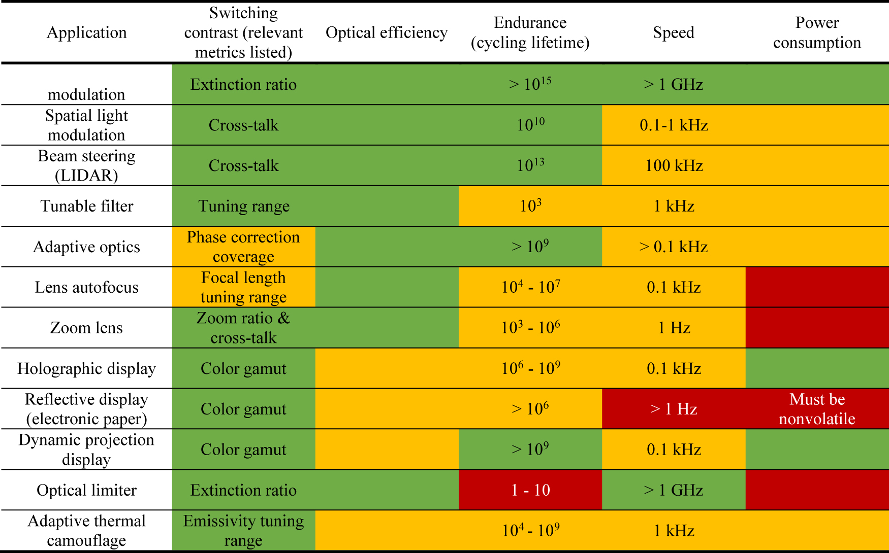
5 Advanced design and optimization: toward multifunctional metasurfaces
By harnessing the electromagnetic multipoles within tunable meta-atoms, their optical responses can be controlled to precisely tailor the output wavefronts. However, such multipole responses can be very complicated and difficult to predict, sometimes even for simple geometries. This challenge escalates when the design domain expands from individual meta-atoms to metasurfaces and multifunctional metadevices. In addition, imperfections originating from material and device fabrication further complicate the design process. As a result, the design space rapidly becomes enormous, and the traditional brute-force searching approach for meta-atoms turns out to be extremely inefficient.
In this section, we discuss advanced design and optimization approaches that can be utilized to potentially address such multifunctional design tasks in an efficient and yet accurate manner. In dielectric metasurfaces, unit cells or meta-atoms are typically comprised of nanoantenna inclusions which are designed to produce a desired set of complex reflection and transmission coefficients [282]. In the optical and IR regimes, these nanoantennas are usually limited to simple canonical shapes such as triangles, rectangles, rings, cylinders, and their combinations. However, it has been shown that nanoantennas based on unintuitive shapes (i.e., free-form geometries) can significantly outperform more traditional geometries in various metrics, such as maximum transmission or reflection magnitudes, phase coverage, field of view, and spectral bandwidth [283], [284]. When paired with active materials, metasurfaces comprised of unintuitive nanoantenna shapes offer the potential to achieve major performance boost across multiple functionalities. The number of design variables used to define a metasurface unit cell also impacts the ability to find optimal solutions; unit cells parametrized with fewer variables are easier to explore than those with larger numbers of variables. Therefore, exploration of the significantly expanded free-form design space necessitates advanced optimization tools and inverse-design strategies [283].
Optimization methods for metadevice design are broadly categorized into local, global, and multi-objective strategies. Local and global algorithms differ in their pursuit of function minima: local algorithms generally fall into local minima, while global algorithms attempt to find the true global minimum. In metadevice design, both local and global algorithms are employed to minimize user-defined cost functions which are used to measure the quality of a given design against a set of predetermined performance criteria. These cost functions are generally hyperdimensional, and their input values are limited to finite ranges in order to incorporate constraints related to the chosen fabrication techniques, materials selection, and SWaP (size, weight, and power) considerations.
While ill-suited for problems with many minima, local optimizers have found success in topology optimization of optical nanoantenna and metasurface designs due to their ability to exploit gradient information generated through adjoint analysis [285], [286], [287], [288], [289], [290], [291], [292]. In particular, topologically optimized multifunctional metagratings were shown to realize wavelength-dependent deflection of incident light into predefined diffraction orders [293]. When building large-area, aperiodic metasurfaces, libraries of topology-optimized unit cells can be constructed and arrayed to stitch the output beams together for desired wavefront shaping [294], such as lensing [295]. Furthermore, free-form metasurfaces with dimensions ≥ 100 wavelengths and multiple layers have been realized, yielding multi-angle and multiwavelength metalens designs [296]. Topology optimization’s greatest strength is its ability to generate relatively free-form geometries due to its lack of strict unit cell parameterization. Still, topology optimization suffers from the same drawbacks that limit local optimizers, namely, the tendency to get stuck in local minima and the inability to optimize highly multimodal problems.
Global optimization algorithms are largely able to overcome these issues. While nearly countless examples of global optimizers exist today, algorithms such as the genetic algorithm (GA) [297], [298], particle swarm optimization (PSO) [299], [300], and the covariance matrix adaptation evolution strategy (CMA-ES) [301], [302], [303] are among the most popular for optical device optimization [283]. Most global optimizers are population-based evolutionary algorithms which update and adapt a population as they explore a function’s response surface to produce new generations better suited to finding the true global minimum. Global optimizers have many advantages over local algorithms, which include forgoing of potentially expensive gradient calculations and applicability to more general and multimodal problems.
Regardless of their specific construction, conventional local and global optimizers generally only seek to optimize a single cost function. Nevertheless, in most cases, engineering problems have multiple competing objectives that designers would like to optimize. With single-objective optimizers (SOOs), the traditional procedure is to include all objectives in a single weighted sum. However, this typically requires a priori knowledge of how best to weight the objectives and can actually eliminate portions of the solution space where the optimizer is unable to explore. Moreover, SOO algorithms yield only a single solution and provide no additional information to the user as to how to judge the design objective tradeoffs inherent to the system. In contrast, multi-objective optimizers (MOOs) such as NSGA-III [304], multi-objective CMA-ES [305], and Borg [306] are able to globally optimize problems with multiple competing cost functions [307]. Furthermore, they produce a collection of solutions called the Pareto set, which contains information about the inherent tradeoffs between design objectives. Finally, it has been shown that optimization is crucially important to maximizing the performance of multifunctional metadevices [205], [308]. To this end, MOO algorithms are ideally suited to this task and form the basis of the proposed reconfigurable metasurface inverse-design process. In Section 7, we show exemplary reconfigurable metasurfaces based on O-PCMs using such optimization approaches.
In addition to optimization techniques, machine learning (ML)–based design methods have emerged as a computationally efficient solution to exploring large design spaces in nanophotonic devcies [309], [310], [311], [312], [313]. One should first collect training data, which contains sets of nanophotonic structures and their respective electromagnetic (EM) responses extracted from full-wave simulations. Then, a neural network (NN) is trained with that data to establish correlations between the parameters and attributes. Once appropriately trained, the NN can perform accurate and rapid prediction of EM responses of a given nanostructure, or inversely, it can search for the design parameters corresponding to the desired response. Therefore, this method enables efficient nanophotonic device evaluation and its design prediction. Overall, ML-assisted design approaches have already shown promising progress in developing a variety of high-performance metasurfaces [310], [314], [315], [316], [317], [318].
Due to the immense DOFs in constructing metasurfaces, early demonstrations using traditional NNs are restricted by the initial training sets with limited geometrical parameters. Generative adversarial network (GAN) methods, which are based on a self-evolving critic evaluating generated designs, allow efficient creation of arbitrary design patterns [319], [320], [321], [322], [323]. Such techniques customized for specific electromagnetic processes with complex meta-atom geometries have also been developed [324], [325], [326], [327], [328]. In the study by Jiang and Fan [324], adjoint variable calculations were incorporated into generative NNs to produce topology-optimized structures through a global search.
When applied to active elements, the ML-assisted approaches were demonstrated to generate efficient designs of multifunctional and reconfigurable metadevices [316], [323], [325]. Encountered by the dramatically enlarged DOFs and associated uncertainties, design constraining rules, which take into account experimental imperfections, have been incorporated in several design frameworks to enhance their robustness [316], [317], [320]. In Section 7, we illustrate the use of ML methods to blueprint multifunctional active metadevice designs based on O-PCMs.
6 Active metadevice design and fabrication: general principles and case studies
The subwavelength pixelated device architecture and capability of on-demand control in principle allow nearly arbitrary wavefront-tuning functionality. In this section, we will focus on nonmechanical active metasurfaces, in which tuning is attained via refractive index change in the material composing meta-atoms.
The operation principles of nonmechanical active metasurfaces can be generally categorized into two groups: individual meta-atom tuning and collective metasurface tuning. The individual meta-atom tuning approach, schematically illustrated in Figure 1a, simplifies unit cell designs by leveraging additional DOFs from the switching matrix. Moreover, individual meta-atom modulation in principle enables arbitrary and continuously tunable optical functions for a single device. However, scalable electrical control of individual meta-atoms remains a major challenge for switching large-area 2-D meta-atom arrays. Alternatively, instantaneous switching of metasurface patches (schematically illustrated in Figure 1b) considerably simplifies the control process. However, the collective modulation scheme, in general, can only achieve switching between a discrete set of states with predefined, albeit arbitrary, optical functions. One embodiment of this approach is to mix meta-atom subarrays designed for different functions on the same aperture region and selectively turn on/off part of the array to allow optical function switching [190]. This “shared aperture” approach, while being straightforward to design and implement, suffers from limitations on optical efficiency and scalability of optical functionalities due to spatial division of the aperture.
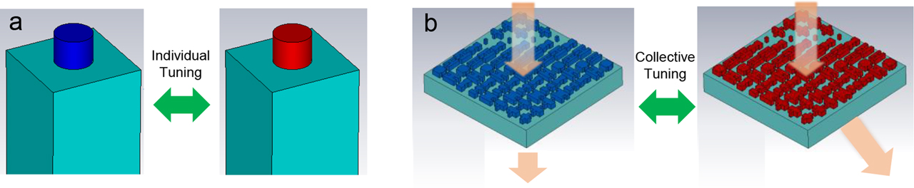
Basic design principles of reconfigurable metadevices: (a) individual meta-atom tuning; (b) collective metasurface tuning. Red and blue colors indicate different optical states of the meta-atoms upon external stimulation.
In this section, we focus on a generic design method enabling full-aperture active phase-gradient metasurfaces via collective tuning: the meta-atoms are individually designed to achieve distinctly variable optical responses upon external stimulations. When switched under a single control signal, collectively they provide variable optical functionalities utilizing the full metasurface aperture. This approach allows the most straightforward control mode, since only one tuning signal is required for each state, but meanwhile, this method requires judiciously designed unit cells and device architectures. Here, we use O-PCM–based all-dielectric metasurfaces to exemplify the design process, strategies and challenges, which cover the essential stages of developing reconfigurable metasurfaces spanning device design, fabrication, calibration, and operation. We note that the design principle is generic and can be applied across all the nonmechanical active metasurface platforms discussed inSection 2.
6.1 O-PCM–based meta-atom modulation: an overview
O-PCMs can be used as either a blanket layer to trigger the mode transitions in metallic structures resting upon them [178], [329], [330], [331] or the building materials of meta-atoms which modulate the transitions directly [175], [332]. In the study by Chen et al [333], a tunable resonator composed of a gold nanodisk array placed on a GST thin layer was designed and experimentally verified. As shown in Figure 2a, dimensions and periodicity of the gold nanodisks, together with the thickness of the GST layer, were carefully chosen to achieve a significant resonance shift in the near IR. This resonance shift enabled a large modulation of the transmitted light intensity of around 50% at 2.4-μm wavelength. Apart from GST, this modulation approach can also be achieved with other materials, such as VO2. In the study by Peng et al [329], a subwavelength gold grating array was deposited on a VO2 film coated on a glass substrate to realize a reconfigurable polarizer (Figure 2b). To maximize the switching efficiency, the transmission properties of the structures were studied through a complete exploration of the parameter scope including the gap g between the gratings, the duty cycle w/p, the height h of the gratings, and the thickness of the VO2 thin film. After an optimal parameter combination was found during the parameter sweep, the high transmission contrast between transverse electric (TE) and transverse magnetic (TM) incidence can be explained by the electric field dissipation behavior revealed by the simulation results.
![Figure 2: Modulation of phase-change/transition material–based meta-atoms: (a) Illustration of a hybrid phase-change plasmonic crystal realized as an array of gold nanodisk on a GST film [333]. (b) Diagram of a linear polarizer consisting of gold gratings deposited on a VO2 film [329]. The geometrical parameters were optimized to achieve the highest switching efficiency and extinction ratio. (c) Drawing depicting two types of patch nanoantennas and their corresponding phase-shift ranges [326]. (d) Top: schematic of a tunable GST nanorod placed on top of a gold substrate. Bottom: maps of phase shifts vs. width and length of GST nanorods in amorphous and crystalline states [332]. GST, Ge–Sb–Te.](/document/doi/10.1515/nanoph-2020-0033/asset/graphic/j_nanoph-2020-0033_fig_002.jpg)
Modulation of phase-change/transition material–based meta-atoms: (a) Illustration of a hybrid phase-change plasmonic crystal realized as an array of gold nanodisk on a GST film [333]. (b) Diagram of a linear polarizer consisting of gold gratings deposited on a VO2 film [329]. The geometrical parameters were optimized to achieve the highest switching efficiency and extinction ratio. (c) Drawing depicting two types of patch nanoantennas and their corresponding phase-shift ranges [326]. (d) Top: schematic of a tunable GST nanorod placed on top of a gold substrate. Bottom: maps of phase shifts vs. width and length of GST nanorods in amorphous and crystalline states [332]. GST, Ge–Sb–Te.
When O-PCMs are used as the building materials of meta-atoms, different multipole resonances can be excited inside the material during the structural transition, which in turn can be utilized to modulate the amplitude and phase of the incident light. Several works have realized optical reconfiguration based on pure amplitude modulations. In the study by Wang et al [334], through harnessing reflection and transmission resonances at specific wavelengths, reconfigurable devices such as multifocus Fresnel zone plates, lenses, and grayscale holograms can be achieved by writing, erasing, and rewriting 2-D binary or grayscale patterns on a GST canvas. More specifically, a continuous relative change of reflectance up to 100% was achieved using excitation laser pulses. In addition to the optical transmission control, Zou et al [335] showed that the structural transition of GST in patch antennas can also trigger continuous phase-shift modulations. In both nanoantenna types shown in Figure 2c which consist of a silver patch placed on GST, continuous phase modulation up to 2π can be achieved by tuning the length of the silver patches. Similarly, Chu et al [332] employed two distinct meta-atoms to augment the phase coverage. The optical structure proposed in this paper consisted of rectangular-shaped GST nanorods placed on a gold mirror with a spacer layer (Figure 2d). A complete parameter sweep of length and width of the GST rods were carried out to find the geometry that yields the largest phase shift of 120° under two different states, respectively. It should be noted that the works described above mostly used parameter sweeping to identify the optimal designs, while strategies on determining other key dimensions such as dielectric layer thickness or period were not mentioned. In Section 7, we outline the limitations of using this prevailing unit cell–searching method and discuss more advanced meta-atom design approaches.
6.2 Metasurface synthetization
Here we discuss the design method of constructing phase-profile reconfigurable metasurface optics via collective tuning. We use a varifocal metalens operating at 5.2-μm wavelength as an example to illustrate the design procedure (Figure 3a), while the same design principle can be adopted for tuning between arbitrary functionalities via wavefront engineering. Key device performance metrics are optical efficiency, contrast ratio, and imaging quality at different optical states. This generic design approach can be used for a variety of meta-atom platforms across different spectral ranges. Assuming N is the number of phase levels covering the 2π phase range and M is the number of switchable metadevice states, then one would need NM distinct meta-atom designs to realize M arbitrary functionalities. In the simplest-case example, two phase levels (i.e., 0° and 180°) are used to sample the 2π phase range; a larger number of phase levels are expected to increase the optical efficiency [9]. For transitioning between the two states (e.g., amorphous and crystalline states of the O-PCM), the metasurface design requires a library of four meta-atoms. Each of the selected meta-atoms provides a distinct combination of two phase values corresponding to the O-PCM states. The selected meta-atoms are then subsequently assembled into a 2-D array to generate the desired phase profiles. The meta-atoms are implemented as all-dielectric Huygens resonators, which feature an ultrathin, deep subwavelength profile that facilitates a simple one-step etching fabrication process [336]. Other types of metasurfaces (e.g., truncated waveguide or geometric-phase antenna) can be utilized as well using the same design framework. GSST was selected as the building block material due to its broadband transparency, large refractive index (n = 3.2–4.7), and large index contrast during phase transition (Δn ∼ 1.5 at 5.2 µm). CaF2 was chosen as substrate material due to its high IR transparency.
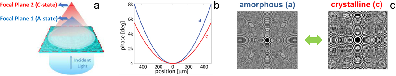
(a) Schematic drawing of a varifocal metalens based on O-PCMs. (b) Ideal hyperbolic phase profiles designed for two focal lengths at different material states. (c) Two-dimensional discretized phase masks at amorphous (left) and crystalline (right) states. Two phase levels, 0° (colored white) and 180° (colored black), are used to sample the 2π phase range. O-PCMs, optical phase-change materials.
In the case of a varifocal metalens, one could first generate hyperbolic phase profiles for the two specified focal lengths by using the following equation [10]:
where λ0 is the wavelength of the incident light, x and y are the coordinates of meta-atoms, and f is the focal length of the metalens at a certain state. The total size of the phase profiles was 1 × 1 mm2, and they were designed to exhibit aberration-free focusing at the focal lengths of f1 = 1 mm and f2 = 1.5 mm for amorphous and crystalline states, respectively. The ideal hyperbolic phase profiles are shown in Figure 3b. The two continuous phase profiles were then discretized in the spatial domain according to the meta-atom arrangement (i.e., with a lattice constant of approximately λ0/2) and in the phase domain into multiple phase levels.
The reconfigurable metalens was designed and modeled utilizing a hierarchical combination of full-wave simulations and Kirchhoff diffraction integral. At the subwavelength scale, full-wave simulations can be implemented to design and model the meta-atoms. With a GSST thickness of 1 µm, a pool of Huygens meta-atoms with various shapes (such as “I” and “+” shapes) were generated in a commercially available full-wave electromagnetic solver (CST Microwave Studio), and a group of four meta-atom structures were chosen based on their phase and amplitude responses at both states (Figure 4a,b). The meta-atoms were designed and generated in compliance with certain design constraints, such as minimum and maximum feature sizes, rounded corners, fabrication tolerance, etc. At the macroscopic level, phase masks were designed and verified using the Kirchhoff integral method to evaluate the metalens performance. Such a model can be further combined with performance figure of merits (FOMs) to guide the selection of meta-atoms and constructing metasurfaces with enhanced optical contrast and efficiencies for the two states, as detailed in the study by Shalaginov et al [192]. The diffraction integral method incorporating the full-wave simulation data enables computationally efficient validation of the optical performance of the entire metalens [336].
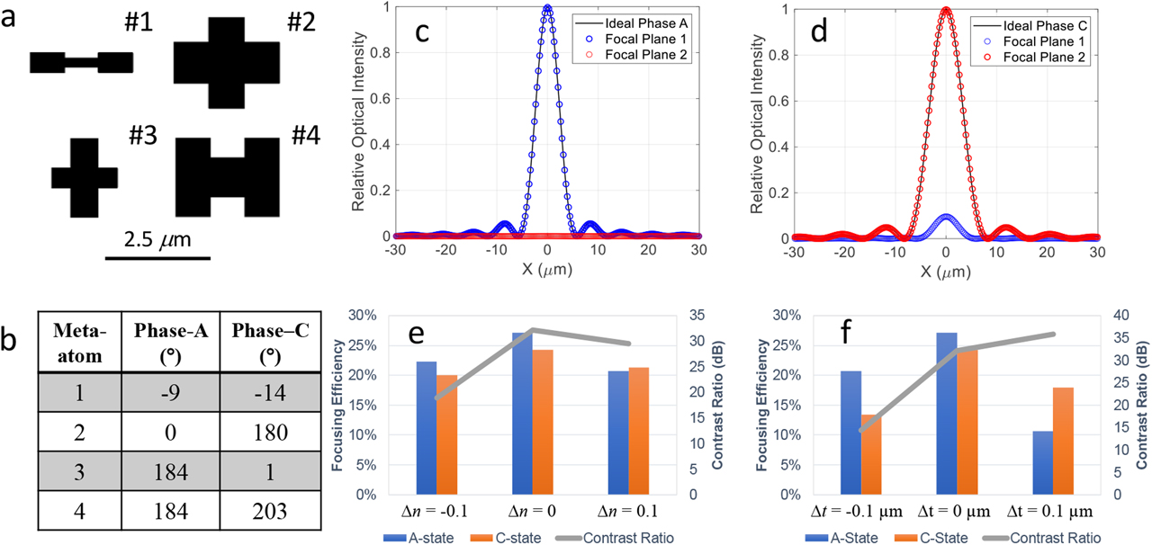
(a) Top view of a group of four GSST Huygens meta-atoms covering 2π phase shift. (b) Each meta-atom provides a distinct combination of the two phase levels close to 0° and 180° in both states. Cross-sectional plots of focal plane optical intensity simulated using the Kirchhoff integral method at (c) amorphous and (d) crystalline states. Sensitivity study of metalens performance (focusing efficiency and contrast ratio) dependence on (e) refractive index variance (Δn) and (f) meta-atom thickness variance (ΔtGSST). GSST, Ge2Sb2Se4Te1.
We modeled the metalens response by using the diffraction integral method and plotted the cross sections of the optical intensities in focal planes 1 and 2 designed for the amorphous and crystalline states, respectively (Figure 4c,d). For comparison, we added the optical intensity curve of the ideal diffraction-limited lens having the same optical parameters. The metalens performance metrics, including focusing efficiency and contrast ratio, are summarized in Figure 4e,f. For the primary focal spots, the focusing efficiencies for amorphous and crystalline states were 27.1 and 24.3%, respectively. The efficiencies are defined as the ratio of the power confined within a radius of 5λ0 to the total power incident on the lens aperture. In contrast to passive meta-optics, the performance of reconfigurable metadevices is further weighted by cross talk across different states. This results in the appearance of phantom images, which are formed by the additional “erroneous” focal spots, and should always be minimized. Cross talk can be quantified by switching contrast ratio (CR) between the two states:
where P1(2),a(c) denotes the focused optical power at focal plane 1 (2) at the amorphous (crystalline) state. The simulation shows a CR of 32.2 dB, indicating negligible cross talk. Another important lens characteristic is the Strehl ratio, which is defined as the ratio of the peak intensity of an evaluated point spread function (PSF) to the peak intensity of a diffraction-limited PSF for an ideal, aberration-free optical system. The Strehl ratios for our varifocal metalens exceed the 0.8 threshold in both states, hence confirming that the metalens operates in the diffraction-limited regime.
The simulation results are consistent with theoretical diffraction efficiency limits of multilevel diffractive optical elements [337] and can be explained by examining the average phase errors and transmittance of the meta-atom group (shown in Table 3). The average phase errors are estimated by subtracting the ideal phase masks from the actual ones and averaging the phase deviations. Since the selected meta-atoms provide phase values at approximately 0° or 180°, any target phase value between 0° and 360° can be sampled using these two phase levels with an averaged error of approximately 45°. Theoretically such a phase sampling accuracy results in maximum diffraction efficiency of about 41%, assuming unity optical transmittance of the meta-atoms [337]. On the other hand, the averaged transmittances of the meta-atoms used to assembly the metasurface are 64.6 and 67.6% for the two states. The theoretically predicted focusing efficiencies of 27.7 and 26.5%, calculated as the products of the diffraction efficiency and the average meta-atom transmittance values, are in excellent agreement with the numerical simulation results. To further improve the optical efficiencies, one can increase the number of phase levels (e.g., 4 and 8 phase levels correspond to 81 and 94.9% maximum diffraction efficiencies, respectively); meanwhile, the overall meta-atom transmittance can be further enhanced.
Simulated focusing efficiency, averaged phase errors, and meta-atom transmittance of the bistate varifocal metalens with two phase levels.
| Amorphous state | Crystalline state | |||
|---|---|---|---|---|
| Focusing eff. | Phase error (avg.) | Focusing eff. | Phase error (avg.) | |
| Focal plane 1 | 27.1% | 44.8° | 2% | 92.4° |
| Focal plane 2 | 0.2% | 91.9° | 24.3% | 45.8° |
| Avg. meta-atom eff. | 67.6% | 64.6% | ||
| Strehl ratio | Close to unity | |||
6.3 Calibration: bridging the gap between numerical models and experimental implementations
Once an initial metasurface design is obtained, a calibration step is essential to identify deviations between the design and fabricated structures. The deviations typically arise from meta-atom geometry and refraction index differences from the assumed values in the model. Here we perform a sensitivity study to illustrate the impact of such deviations by introducing refractive index and thickness variances (Δn = ±0.1 and ΔT = ±0.1 μm, respectively) to the numerical models of the varifocal metalens. The simulation results are summarized in Figure 4e,f. The optical responses (both amplitude and phase) of the Huygens meta-atoms exhibit strong dependence upon such disturbances due to the locally induced resonance shifts at both amorphous and crystalline states, resulting in up to ∼60 and ∼55% relative reduction on metalens focusing efficiency and contrast ratio (in dB). In particular, phase deviations not only reduce diffraction efficiencies but also exacerbate cross talk between the two states. Therefore, to fully account for the impact of such imperfections, it is important to quantify the deviations of meta-atom geometry and material optical properties from the design model values.
The meta-atom geometry deviation usually originates from the material deposition and lithographic patterning process. The typically observed fabrication imperfections are thickness variance, angled sidewalls, surface roughness, edge rounding, etc. To quantify such deviations, we calibrated the metasurface design by importing the “as-fabricated” geometries into the numerical models. Shapes and, subsequently, the contour profiles of the fabricated meta-atoms were retrieved from scanning electron microscope (SEM) images. As illustrated in Figure 5a–d, the original top-view SEM image was processed using image processing tools to extract contour profiles of the top and bottom of the meta-atoms. Additional details can be retrieved from the angled SEM images (Figure 5e) to reconstruct 3-D geometries fully resembling the fabricated meta-atoms (see Figure 5f). The 3-D “as-fabricated” model incorporating all geometric deviations was subsequently fed back to full-wave simulation tools to re-evaluate and optimize their optical responses. Consequently, the geometric mismatch between design and fabrication can be effectively minimized to realize metasurfaces with “as-planned” functionalities and sufficient tolerance to imperfections.
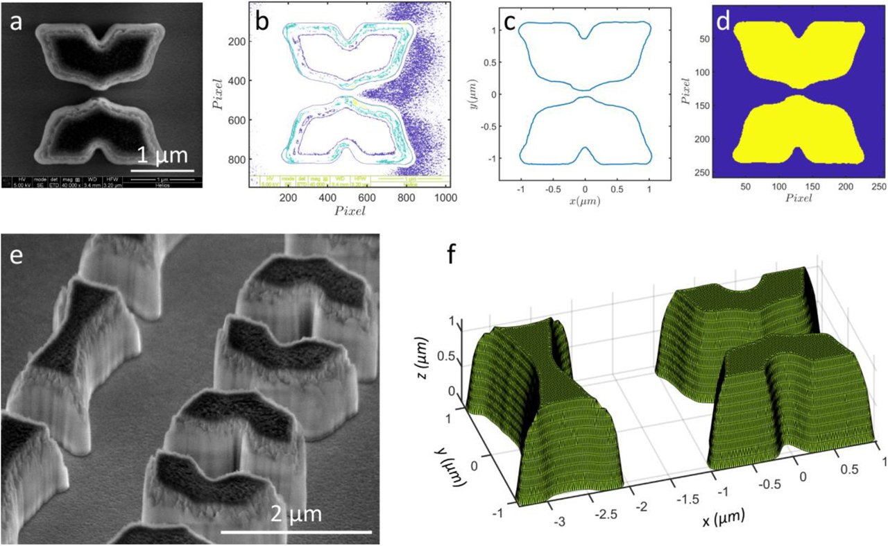
Generation of 3-D meta-atom geometry from scanning electron microscope (SEM) images of fabricated samples. (a) SEM top-view image of an exemplary meta-atom. (b) Image processing technique to identify the possible boundaries. (c) Subsequent extraction of the bottom contour. (d) Binary image of the meta-atom cross section. (e) Angled-view SEM micrograph depicting the sidewall shape. (f) Three-dimensional geometry resembling the as-fabricated meta-atom.
Another source of potential deviation between the numerical model and experimental results is the refractive index and its dispersion in fabricated devices. In an exemplary calibration protocol, the film thickness is first measured using a stylus profilometer. Then the precalibrated film is patterned and fabricated into periodic arrays of nanodisk antennas with various diameters. These antennas are designed to produce distinct resonances, which originate from the excitation of multipole modes inside the dielectric nanodisks. Using a commercial spectrophotometer setup, the transmittance spectra are subsequently measured and fitted with the simulated data, where the refractive index is adjusted so that the simulations match well the experimental results. The same calibration procedure can be performed for samples under different states.
7 Implementation of advanced design and optimization approaches
In the example discussed in Section 6, we adopted a traditional parameter sweeping approach to identify the active meta-atom design. Building a meta-atom library for such multistate metasurfaces poses a multi-objective optimization challenge which is far more difficult than constructing a passive metasurface design. Additionally, the number of meta-atoms needed increases exponentially with the number of states. In reality, the accessibility of optimal meta-atoms may be limited by the pool of candidates obtained from full-wave simulations. These difficulties render the traditional parameter sweeping approach highly inadequate. In this section, we will discuss the implementation of advanced meta-atom design and searching methods to accelerate and improve the design process.
7.1 Multi-objective optimization for reconfigurable metasurface synthesis
In this section, a multi-objective optimization enabled design framework is proposed for the efficient generation of multifunctional meta-atoms based on O-PCMs. Two exemplary reconfigurable dielectric metasurface devices are then presented in order to advocate the efficacy of the proposed optimization framework. Importantly, while here we choose O-PCM–based active metasurfaces to illustrate the optimization process, these algorithms are broadly applicable to other tuning mechanisms summarized in Table 1 that modulate the optical responses of meta-atoms.
As discussed in Section 5, MOO algorithms are ideally suited to the design tasks of multifunctional metadevices, an overview of which can be found in Figure 6. The goal of the proposed inverse-design and optimization process is to synthesize reconfigurable metasurfaces either directly, if time permits and sufficient computational resources exist, or, more commonly, through the generation of a “periodic table” of meta-atoms which can later be aperiodically tiled to form a complete metasurface. The process begins with the initialization of the optimizer, which generates an initial set of candidate meta-atoms to simulate. The next step is to enforce several, or all design constraints (e.g., minimum feature size, radius of curvature, etc.), and alter the meta-atom geometries accordingly. For simplicity and speed of simulation, meta-atoms are then evaluated under plane wave illumination with doubly periodic boundary conditions which mimic their behavior in an infinite array. Next, data (e.g., complex transmission and reflection coefficients) are gathered from the simulations and are used to evaluate a set of predetermined cost functions which the optimizer seeks to minimize. The values generated by the cost functions are then used to evaluate end (stopping) condition (e.g., maximum allowed function evaluations or other convergence criteria). Finally, data are fed back to the optimizer and the process repeats until the end condition is met. When the process is finished, a Pareto set of solutions is generated, which in the hypothetical example shown in Figure 6 showcases the tradeoffs between the performances achievable at binary states of the O-PCM. Finally, these solutions are used to populate the periodic table of elements.
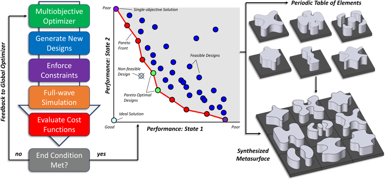
Flowchart showing the multi-objective optimization-powered process for synthesizing multifunctional metasurfaces based on O-PCMs. Once the (left) optimization process is complete, a set of solutions (middle) is presented to the user. The blue dots represent feasible designs while the purple, red, and green dots represent Pareto optimal designs. All of these designs can be used to generate a periodic table of elements (right top) which form the basis for synthesizing a complete metasurface (bottom right). O-PCMs, optical phase-change materials.
As previously discussed, the performance achievable by the optimized meta-atoms is highly dependent on what geometrical inclusions they can assume. While topology optimization is an attractive option for generating unintuitive meta-atom shapes, it is challenging to pair it with global optimization algorithms. Nevertheless, the ability to generate relatively free-form geometries, while simultaneously exploiting the global robustness and multi-objective support afforded to us by state-of-the-art optimizers, is highly desired. To this end, we employ a level-set method based on Bèzier surfaces, which has been shown to offer extraordinary geometrical flexibility while only requiring a few variables to define the surface [338]. Moreover, these surfaces are readily optimizable with global and multi-objective algorithms, making them an ideal choice for generating reconfigurable and multifunctional meta-atoms. An overview of the meta-atom generation process is provided in Figure 7. The generated 3-D control surface is first converted to a binary representation to determine the meta-atom borders. These 2-D outlines are then vertically extruded to realize initial 3-D shapes. Next, predefined fabrication constraints can be enforced. The sharp corners of the original design are rounded to meet some hypothetical fabrication specification while yielding the added benefit of removing areas that may produce significant field enhancements. Additional constraints can then be employed to leave only the largest island and further eliminate narrow areas. These geometrical alterations can be applied via a combination of simple matrix manipulations and image processing techniques before extrusion.
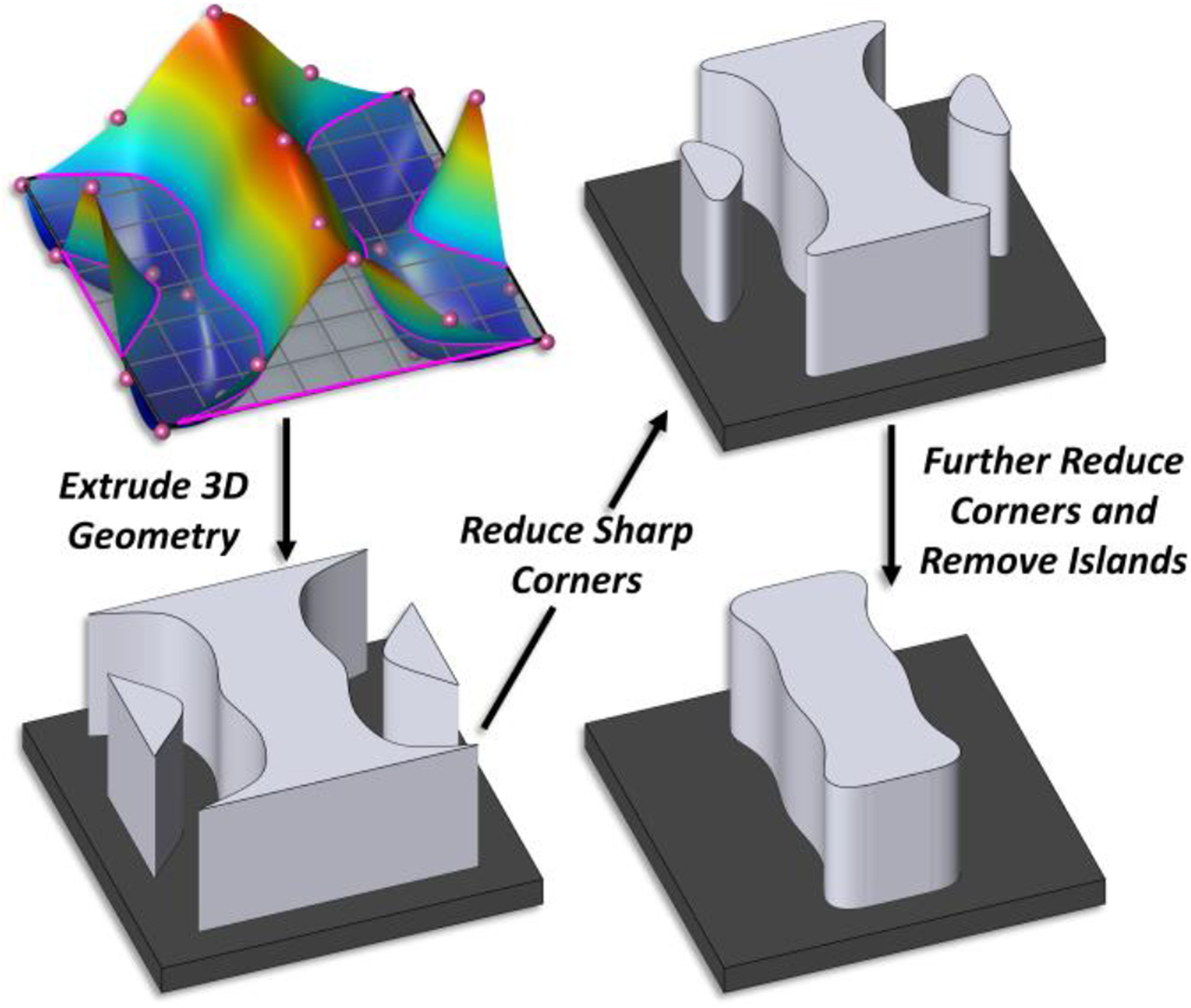
Meta-atom generation process: (top left) a Bèzier control surface which is intersected by a level-set plane to determine the meta-atom border, (bottom left) extruded 3-D meta-atom, (top right) initial application of fabrication constraints to remove sharp corners, and (bottom right) application of additional constraints to remove small islands.
The proposed optimization framework is general enough to be applied to a tremendous variety of multifunctional and reconfigurable metasurface problems. To test the efficacy of the proposed framework, two exemplary reconfigurable metasurface-based devices are presented further, along with thorough discussions of the optimization and performance results.
7.2 Exemplary reconfigurable dielectric meta-optic design based on O-PCMs
Perhaps the most exciting aspect of optical nanoantennas is their ability to offer simultaneous control over amplitude and phase (and polarization) [339]. In traditional optical devices, one normally would not want to tune the amplitude since that always means a decrease in the transmitted power which can negatively affect system performance. However, in reconfigurable metasurfaces, control over both amplitude and phase is extremely desirable. For example, one could design a metadevice to have large transmission or reflection in one state and no transmission or reflection in another. Also, a device could be synthesized to switch from transmitting to reflecting modes or provide on-demand tunable beam-steering capability.
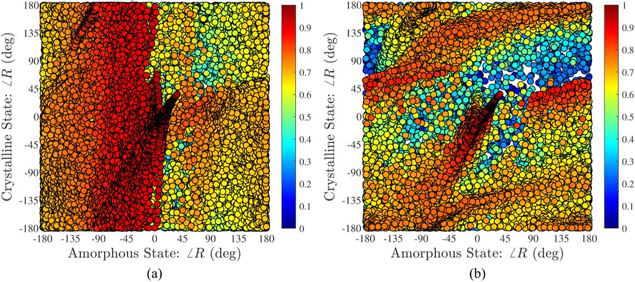
We first take GST, the classical O-PCM, as an example. In the study by Pogrebnyakov et al [205], a meta-atom was developed using a genetic algorithm to achieve high transmission when the GST was in its amorphous state and high absorption in its crystalline state. Using the material data from the study by Pogrebnyakov et al [205], the proposed multi-objective optimization framework was employed to generate an unintuitive unit cell with the same objectives, albeit with a different periodicity and material thickness and for a wavelength of 1.55 µm. The unit cell was illuminated with a linearly polarized plane wave normally incident from the top (air side). The period was set to be 800 nm and the thickness 250 nm. The refractive indices of the constituent materials at 1.55 µm were 1.444 for SiO2 as well as 4.164 + 0.140i and 7.722 + 2.271i for GST in its amorphous and crystalline states, respectively. The GST layer patterning was generated using the proposed design method with 5 × 5 uniformly spaced control points while enforcing fourfold symmetry and optimized using a state-of-the-art multi-objective optimizer, Borg [306], with two objectives: maximizing (1) amorphous state transmission and (2) crystalline state absorption. Figure 8 shows the optimization results. Each circle represents a different meta-atom geometry simulated with a full-wave Maxwell solver employing doubly periodic boundary conditions. Looking at Figure 8, the ideal solution would be a dark blue circle in the top right corner, which would correspond to a design that achieves complete transmission and absorption in the amorphous and crystalline state, respectively. However, due to losses in the amorphous state and unwanted reflection/transmission in the crystalline state, this ideal solution is unattainable. Fortunately, as one can see, there is a range of solutions that nearly achieve this goal with differing amounts of tradeoff between the two objectives. Note that higher transmittance values in the amorphous state leads to a reduction of crystalline state absorption. These designs (near the bottom right of the figure) contain very little GST material which is the cause of their low loss values. If one wants to minimize the power transmitted in the crystalline state (blue color), then one must accept a slight reduction in the maximum transmittance in the amorphous state. From Figure 8, one can see that the transmittance achieved in the crystalline state can be quite low (dark blue), indicating a very strong spectral filtering effect in this reconfigurable device.
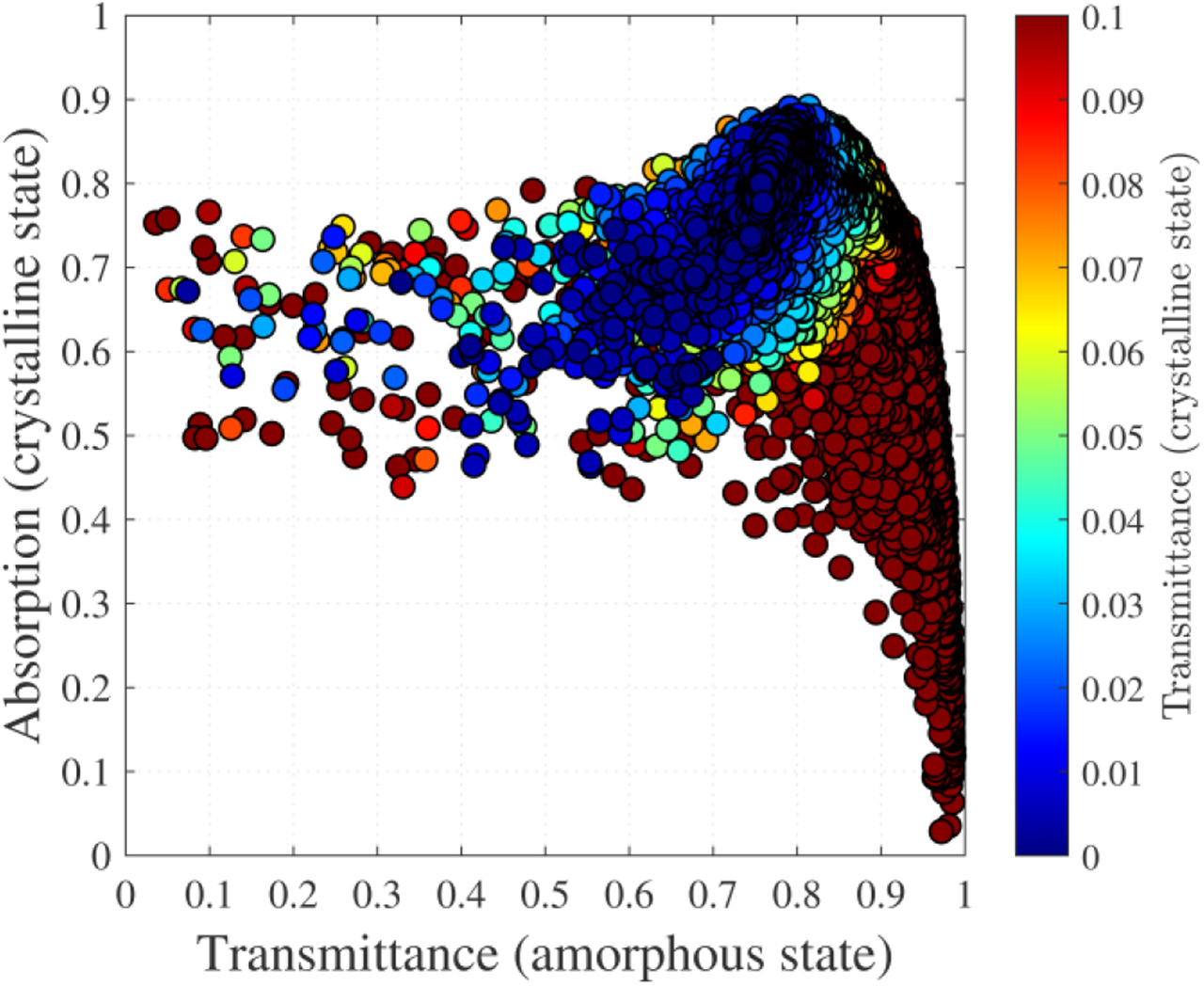
Multi-objective results for the GST active metasurface unit cell optimization. Each dot represents a unique unit cell geometry, and their color indicates the transmittance in the crystalline state. The data show the tradeoffs between the achievable crystalline state absorption and amorphous state transmittance. GST, Ge–Sb–Te.
From the data set shown in Figure 8, one of the best performing designs was selected for further examination. Figure 9 summarizes the reflectance, transmittance, and absorption of a homogeneous GST slab on an infinite SiO2 substrate and compares it to that of the optimized metasurface unit cell. Both simulations were performed using COMSOL Multiphysics v5.3 [340]. One sees that the optimized design achieves a significant enhancement in the absorption magnitude through intelligent patterning of GST. This confirms that the optimized design enhances the intrinsic behaviors of GST in both states. Interestingly, while the homogeneous GST slab is highly reflective due to its large refractive index, the patterned-GST layer has a very low reflection in both states. However, in the amorphous state, the loss is significantly less than in the crystalline state, which is why the transmission and absorption are so pronounced in these states, respectively. In the amorphous state, the optimized unit cell achieves broad transmission behavior while the crystalline state has a broad absorption behavior with very low transmission. Such a device could be used as an optical switch, a nonmechanical shutter or a spectral filter in an imaging system.
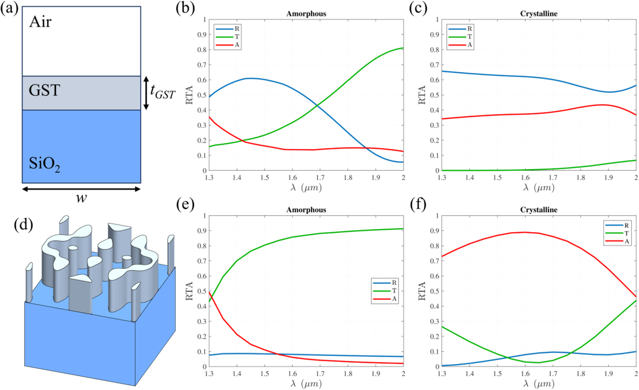
(a) Cross-sectional view of the homogeneous GST slab on an infinite SiO2 substrate. The reflectance, transmittance, and absorption (RTA) spectra of the GST slab unit cell in the (b) amorphous (c) crystalline states. (d) The patterned-GST meta-atom which maximizes transmission in the amorphous state and absorption in the crystalline state at the 1.55-μm wavelength. The RTA spectra of the optimized metasurface in the (e) amorphous and (f) crystalline states. GST, Ge–Sb–Te.
The proposed MOO framework can also be employed to efficiently generate a periodic table of meta-atoms that each offer a unique optical response. The elements of this periodic table can then be used as building blocks to synthesize complete metasurfaces. Diffraction efficiency measures the percentage of incident power the metasurface can steer into a desired transmitted or reflected diffraction order and is an important metric to judge metasurface performance. To this end, dielectric metasurfaces are extremely desirable for their low loss [341], which can be exploited to achieve very high diffraction efficiency [342]. As discussed earlier, reconfigurable meta-optics using traditional O-PCMs, such as GST, are inherently limited by high material absorption losses. Fortunately, another O-PCM GSST offers a large refractive index change when switching from the amorphous to crystalline states, while still maintaining low loss [211], [343]. The reduced loss makes GSST an enticing material option for high-efficiency transmissive and reflective reconfigurable metasurfaces [192].
In the second example, we design a GSST reconfigurable phase-gradient metasurface operating at 5.2-µm wavelength. As a first step, a multi-objective optimization was carried out to find the best performing meta-atoms in both states of GSST. The meta-atoms were simulated at a design wavelength of 5.2 µm and with a period of 2.548 µm. A normally incident linearly polarized plane wave illumination was imposed on the GSST layer from the top. The unit cell was comprised of a 1-µm GSST layer on top of a 200-nm platinum layer with permittivity ϵr = −409.96 + 178.69i [344]. The thick platinum layer effectively serves as a ground plane to prevent transmission and is electrically heated to change the GSST material state. The GSST permittivity is ϵr = 12.16 + 0.1213i and ϵr = 19.03 + 0.1658i in the amorphous and crystalline states, respectively. As in the previous example, the meta-atom designs were created using the synthesis methods described above.
The data shown in Figure 10 indicate that a tremendous variety of solutions exist owing to the low loss and large tunability of GSST. Each dot represents a unique meta-atom geometry, and the dot color represents the reflectance in the amorphous and crystalline states (Figure 10a,b), respectively. Since the purpose of this design is to achieve a high-reflection-efficiency reconfigurable metadevice, the dots with the highest reflection magnitudes are plotted on top of other designs. It should be noted that in both states, there exist meta-atom geometries that achieve a range of reflection magnitudes in addition to reflection phases. The goal in designing these meta-atoms is to create a reconfigurable beam-steering metasurface where, in the amorphous state, the incident light is reflected into the −1 diffraction order, and in the crystalline state, the light is normally reflected (0th order).
The meta-atom reflection phase for the two states with the colorbar indicating the reflectance for the (a) amorphous and (b) crystalline states. Each circle represents a different meta-atom design whose reflection phase in the amorphous and crystalline state are plotted along the x- and y-axes, respectively. The colors represent the reflectance magnitude in the (a) amorphous and (b) crystalline states.
To synthesize the beam-steering device, only geometries that achieve large reflection magnitudes in both states are considered. The meta-atoms were chosen to achieve a linear phase gradient in the amorphous state while simultaneously maintaining a fixed reflection phase in the crystalline state. The chosen meta-atoms were combined into a supercell (see Figure 11a) whose x- and y-periods are 7.644 and 2.548 µm, respectively. The synthesized design achieved diffraction efficiencies of 72.2 and 79.9% in the −1 and 0 diffraction orders for the amorphous and crystalline states, respectively (Figure 11b). The reflectarray design also exhibits high contrast ratio of 23 dB. The ripple in the reflected waves seen in Figure 11c is due to the presence of minor contributions from the other undesired diffraction orders. These results serve to demonstrate the power of the proposed reconfigurable metasurface framework.
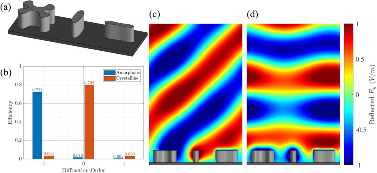
GSST reconfigurable reflectarray. (a) The finalized supercell design over a platinum substrate. (b) Diffraction efficiencies for the optimized GSST-based supercell design in the (blue) amorphous and (orange) crystalline states. Electric field plots in the vicinity of the supercell in the (c) amorphous and (d) crystalline states. GSST, Ge2Sb2Se4Te1.
7.3 Multifunctional meta-atoms design using deep neural networks (DNNs)
As discussed earlier, building a meta-atom library serving multistate metasurface designs is significantly more challenging than performing the same task for a passive metasurface. The extra complexity arises from the need to fulfill multiple design objectives, thereby demanding an exponentially increased number of meta-atoms. Additionally, the requirements for phase and amplitude precision, as well as tolerance to fabrication and operation deviations, become even more stringent in order to avoid cross talk and efficiency reduction during the state transition. While the MOO techniques enable the exploration of significantly expanded design spaces, it is also highly desirable to develop design generation and validation tools in place of full-wave electromagnetic modeling to complement the optimization algorithms and enhance the design throughput.
A recently emerged DNN-based metasurface design and characterization approach [316], [323], [328] offers a promising solution to address the design throughput challenge. In the study by An et al [316], an all-dielectric reconfigurable meta-atom design based on NNs was presented. After training with data, the meta-atom performance predicting NNs can rapidly evaluate phase and amplitude responses of nanodisks of various radii, heights, periods, and refractive indices over a broad spectral band. A closed-loop NN, illustrated in Figure 12a, was constructed to generate meta-atom designs with on-demand optical responses. In this NN, the model generator produces a meta-atom structure, which is then fed to the predicting neural network to assess their amplitude and phase responses. The response data are then sent back to the model generator, where a new meta-atom structure is produced with the goal of reducing the difference between the current and the desired meta-atom responses. The process reiterates until a satisfactory meta-atom design is reached. The model generator can be readily modified to meet diverse design requirements. By leveraging this design framework, a cylinder-shaped meta-atom structure yielding over 310° phase coverage, while its refractive index continuously varies from 3.5 to 4.5, was obtained within several minutes of computation time (Figure 12b). With conventional approaches, convergence to similar designs would require intensive parameter sweeping and elaborate field distribution analysis, which can easily take hours or days [345].
![Figure 12: Multifunctional meta-atom design using deep neural networks (DNNs). (a) Schematic illustrating the process of meta-atom design generation by employing predictive neural networks [316]. (b) Top: transmission amplitude and phase responses of cylinder-shaped all-dielectric meta-atoms in the continuous range of material states (n = 3.5–4.5) at 5.2-μm wavelength. Bottom: diagram of electric (arrows) and magnetic (color coded) fields inside the meta-atom in the states #1 and #4 (indicated on the polar plot above). Incident light propagation direction is marked with an orange arrow [316]. (c) Artistic rendering and layout of a polarization-multiplexed, transmissive bifocal lens designed with DNNs [323]. Focal lengths for x-polarized and y-polarized incidences are 80 and 60 μm, respectively. A quarter of the metalens layout is shown at the bottom, where the yellow areas correspond to the dielectric meta-atoms.](/document/doi/10.1515/nanoph-2020-0033/asset/graphic/j_nanoph-2020-0033_fig_012.jpg)
Multifunctional meta-atom design using deep neural networks (DNNs). (a) Schematic illustrating the process of meta-atom design generation by employing predictive neural networks [316]. (b) Top: transmission amplitude and phase responses of cylinder-shaped all-dielectric meta-atoms in the continuous range of material states (n = 3.5–4.5) at 5.2-μm wavelength. Bottom: diagram of electric (arrows) and magnetic (color coded) fields inside the meta-atom in the states #1 and #4 (indicated on the polar plot above). Incident light propagation direction is marked with an orange arrow [316]. (c) Artistic rendering and layout of a polarization-multiplexed, transmissive bifocal lens designed with DNNs [323]. Focal lengths for x-polarized and y-polarized incidences are 80 and 60 μm, respectively. A quarter of the metalens layout is shown at the bottom, where the yellow areas correspond to the dielectric meta-atoms.
Reconfigurable meta-atom designs are usually composed of simple canonical shapes, such as cylinders [333], bars [329], [335], and gratings [187], [329], which have a narrow space of variable design parameters leading to limited metadevice performance. Fortunately, NN approach incorporating GANs can dramatically increase the design DOFs by exploring free-form meta-atom geometries. A recent paper discusses the possibility of using GANs to produce free-form all-dielectric multifunctional meta-atoms and entire metadevices [323]. As a demonstration, this method was tested on the design of a polarization-multiplexed bifocal lens (Figure 12c), whose performance was further verified with full-wave simulations. By using the training data, including phase and amplitude responses of meta-atoms at different material states, a reconfigurable meta-atom design network can be constructed based on this framework. This novel approach is extremely time-efficient (i.e., on-demand meta-atoms can be produced within milliseconds) and allows exploration of numerous design degrees of free-form with meta-atom geometries. We envision that this approach will empower the process of designing metasurfaces, especially those with multifunctional and reconfigurable features.
8 Outlook
As we have elaborated in this review, active metasurfaces have taken major strides over the past decade, and the technology is maturing to the point where it is ready to make an impact on practical applications. Indeed, in very recent years, several startup companies such as Tunoptix [346] and Lumotive [347] have emerged seeking to commercialize various active metasurface technologies, a growing trend we will likely witness in the near future. It, therefore, comes as no surprise that the research emphasis in the area is starting to transition from exploring different optical modulation mechanisms to perfecting the meta-optics performance such that they can start to compete with and even topple their traditional bulk counterparts. This paradigm shift prompts the organization of our discussions herein and the O-PCM metasurface design example, through which we aim to highlight the useful techniques in optical engineers’ toolbox for developing active meta-optics with high optical quality.
Besides optical quality, scalability is another key challenge that must be addressed for active metasurfaces. In many examples of active metasurfaces cited here, the optics were demonstrated with apertures of the order of tens of microns or even smaller. Scaling to much larger areas (mm to cm scale), which are the norm for most practical optical systems, is important for two reasons. First, the optical performance measured on small-aperture optics might not be representative of the same design with larger apertures. This is in part because fabrication nonuniformity is often exacerbated with large areas, and in part, because optical aberrations also scale with increasing aperture size in optical systems where systematic deviations from the ideal diffraction-limited phase profiles are present. Additionally, large aperture size also presents a hurdle toward electrical addressing of meta-atoms, which is probably the preferred active tuning scheme for many practical applications. The collective switching scheme illustrated in Figure 1a faces possible challenges associated with large-area uniformity and multistate tuning, whereas the individual meta-atom addressing scheme (Figure 1b) is hardly practical given the extremely large number of meta-atoms (easily exceeding 108) in macroscopically sized optics. The subwavelength meta-atom pitch and large array size may further pose stringent requirements on (electrical or thermal) cross talk suppression. We, therefore, anticipate that the solution may entail some “hybrid” switching configurations combining features from both schemes – offering adequate spatial granularity to facilitate continuous or quasi-continuous multistate tuning while leverages collective switching of groups of meta-atoms to mitigate the electrical addressing complexity. Specifically, the symmetry of the optics can be harnessed to minimize the number of independent electrical controls. For instance, a varifocal metalens with continuously variable focal length can be realized by modulating meta-atoms grouped on a series of concentric ring–shaped electrodes given circular symmetry of the lens. An alternative strategy involves mapping the optical functions into two orthogonal directions. As an example, a 2-D metalens can be synthesized from two orthogonally arranged 1-D cylindrical metalenses with considerably reduced electrical routing complexity.
Finally, performance consistency, integration compatibility, and manufacturability are among other important metrics that researchers should strive to improve to enable active metasurface technologies that will make a tangible impact on practical applications.
9 Conclusion
Active metasurfaces possessing a flat, pixelated device architecture enable local and global optical response tuning, thus introducing new opportunities for dynamic wavefront control. In this review, we survey recent progress in reconfigurable metasurface optics, which covers tuning mechanisms, material platforms, and design approaches. We outline key device metrics and review outstanding questions and gaps. Using O-PCM–based active metasurface as an example, we outline a generic design principle for all-dielectric, collectively tuned, reconfigurable metasurfaces. Advanced unit cell optimization tools and design approaches are also discussed to address the escalating design complexity with active metasurfaces. The multiscale, multiphysics, and multi-objective wholistic design framework presented herein is expected to inspire new designs enabling meta-optical devices with unprecedented optical quality, and expedite their deployment in practical reconfigurable optical systems.
Funding source: Penn State MRSEC, Center for Nanoscale Science
Award Identifier / Grant number: NSF DMR-1420620
Funding source: Defense Advanced Research Projects Agency
Award Identifier / Grant number: HR00111720029
Acknowledgements
Funding support is provided under Defense Advanced Research Projects Agency Defense Sciences Office (DSO) Program: EXTREME Optics and Imaging (EXTREME) under Agreement No. HR00111720029. This work was also supported in part by the Penn State MRSEC, Center for Nanoscale Science, under Award No. NSF DMR-1420620.
Author contribution: All the authors have accepted responsibility for the entire content of this submitted manuscript and approved submission.
Research funding: Funding support is provided under Defense Advanced Research Projects Agency Defense Sciences Office (DSO) Program: EXTREME Optics and Imaging (EXTREME) under Agreement No. HR00111720029. This work was also supported in part by the Penn State MRSEC, Center for Nanoscale Science, under Award No. NSF DMR-1420620.
Conflict of interest: The authors declare no conflicts of interest regarding this article.
References
[1] N. Yu, P. Genevet, M. A. Kats, et al., “Light propagation with phase discontinuities: generalized laws of reflection and refraction,” Science, vol. 334, pp. 333–337, 2011. https://doi.org/10.1126/science.1210713.Search in Google Scholar PubMed
[2] N. Yu and F. Capasso, “Flat optics with designer metasurfaces,” Nat. Mater., vol. 13, pp. 139–150, 2014. https://doi.org/10.1038/nmat3839.Search in Google Scholar PubMed
[3] A. V. Kildishev, A. Boltasseva, and V. M. Shalaev, “Planar photonics with metasurfaces,” Science, vol. 339, pp. 12320091–12320096, 2013. https://doi.org/10.1126/science.1232009.Search in Google Scholar PubMed
[4] S. M. Kamali, E. Arbabi, A. Arbabi, and A. Faraon, “A review of dielectric optical metasurfaces for wavefront control,” Nanophotonics, vol. 7, pp. 1041–1068, 2018. https://doi.org/10.1515/nanoph-2017-0129.Search in Google Scholar
[5] P. Lalanne and P. Chavel, “Metalenses at visible wavelengths: past, present, perspectives,” Laser Photonics Rev., vol. 11, 2017 https://doi.org/10.1002/lpor.201600295.Search in Google Scholar
[6] S. B. Glybovski, S. A. Tretyakov, P. A. Belov, Y. S. Kivshar, and C. R. Simovski, “Metasurfaces: from microwaves to visible,” Phys. Rep., vol. 634, pp. 1–72, 2016. https://doi.org/10.1016/j.physrep.2016.04.004.Search in Google Scholar
[7] D. Neshev and I. Aharonovich, “Optical metasurfaces: new generation building blocks for multi-functional optics,” Light Sci. Appl., vol. 7, p. 58, 2018. https://doi.org/10.1038/s41377-018-0058-1.Search in Google Scholar PubMed PubMed Central
[8] H.-H. Hsiao, C. H. Chu, and D. P. Tsai, “Fundamentals and applications of metasurfaces,” Small Methods, vol. 1, p. 1600064, 2017. https://doi.org/10.1002/smtd.201600064.Search in Google Scholar
[9] F. Aieta, P. Genevet, M. Kats, and F. Capasso, “Aberrations of flat lenses and aplanatic metasurfaces,” Opt. Express, vol. 21, pp. 31530–31539, 2013. https://doi.org/10.1364/oe.21.031530.Search in Google Scholar
[10] F. Aieta, P. Genevet, M. A. Kats, et al., “Aberration-free ultrathin flat lenses and axicons at telecom wavelengths based on plasmonic metasurfaces,” Nano Lett., vol. 12, pp. 4932–4936, 2012. https://doi.org/10.1021/nl302516v.Search in Google Scholar PubMed
[11] W. T. Chen, A. Y. Zhu, V. Sanjeev, et al., “A broadband achromatic metalens for focusing and imaging in the visible,” Nat. Nanotechnol., vol. 13, pp. 220–226, 2018. https://doi.org/10.1038/s41565-017-0034-6.Search in Google Scholar PubMed
[12] S. Wang, P. C. Wu, V.-C. Su, et al., “Broadband achromatic optical metasurface devices,” Nat. Commun., vol. 8, pp. 1–9, 2017. https://doi.org/10.1038/s41467-017-00166-7.Search in Google Scholar PubMed PubMed Central
[13] S. Shrestha, A. C. Overvig, M. Lu, A. Stein, and N. Yu, “Broadband achromatic dielectric metalenses,” Light Sci. Appl., 2018. https://doi.org/10.1038/s41377-018-0078-x.Search in Google Scholar PubMed PubMed Central
[14] Y. Zhou, I. I. Kravchenko, H. Wang, J. R. Nolen, G. Gu, and J. Valentine, “Multilayer noninteracting dielectric metasurfaces for multiwavelength metaoptics,” Nano Lett., vol. 18, pp. 7529–7537, 2018. https://doi.org/10.1021/acs.nanolett.8b03017.Search in Google Scholar PubMed
[15] J. Engelberg, C. Zhou, N. Mazurski, J. Bar-David, A. Kristensen, and U. Levy, “Near-IR wide-field-of-view Huygens metalens for outdoor imaging applications,” Nanophotonics, vol. 9, no. 2, pp. 361–370, 2020. https://doi.org/10.1515/nanoph-2019-0177.Search in Google Scholar
[16] A. Arbabi, E. Arbabi, S. M. Kamali, Y. Horie, S. Han, and A. Faraon, “Miniature optical planar camera based on a wide-angle metasurface doublet corrected for monochromatic aberrations,” Nat. Commun., vol. 7, pp. 1–31, 2016. https://doi.org/10.1038/ncomms13682.Search in Google Scholar PubMed PubMed Central
[17] B. Groever, W. T. Chen, and F. Capasso, “Meta-lens doublet in the visible region,” Nano Lett., vol. 17, pp. 4902–4907, 2017. https://doi.org/10.1021/acs.nanolett.7b01888.Search in Google Scholar PubMed
[18] M. Y. Shalaginov, S. An, F. Yang, et al., “A single-layer panoramic metalens with >170 degree diffraction-limited field of view,” 2019, arXiv: 1908.03626. https://doi.org/10.1364/fio.2019.fm4c.1.Search in Google Scholar
[19] L. Kang, R. P. Jenkins, and D. H. Werner, “Recent progress in active optical metasurfaces,” Adv. Opt. Mater., p. 1801813, 2019. https://doi.org/10.1002/adom.201801813.Search in Google Scholar
[20] A. Nemati, Q. Wang, M. Hong, and J. Teng, “Tunable and reconfigurable metasurfaces and metadevices,” Opto-Electronic Adv., vol. 1, pp. 18000901–18000925, 2018. https://doi.org/10.29026/oea.2018.180009.Search in Google Scholar
[21] H.-T. Chen, A. J. Taylor, and N. Yu, “A review of metasurfaces: physics and applications,” Reports Prog. Phys., vol. 79, no. 7, p. 76401, 2016. https://doi.org/10.1088/0034-4885/79/7/076401.Search in Google Scholar PubMed
[22] C. U. Hail, A. U. Michel, D. Poulikakos, and H. Eghlidi, “Optical metasurfaces: evolving from passive to adaptive,” Adv. Opt. Mater., p. 1801786, 2019. https://doi.org/10.1002/adom.201801786.Search in Google Scholar
[23] A. M. Shaltout, A. V. Kildishev, and V. M. Shalaev, “Evolution of photonic metasurfaces: from static to dynamic,” J. Opt. Soc. Am. B, vol. 33, p. 501, 2016. https://doi.org/10.1364/josab.33.000501.Search in Google Scholar
[24] Q. He, S. Sun, and L. Zhou, “Tunable/reconfigurable metasurfaces: physics and applications,” Research, vol. 2019, pp. 1–16, 2019. https://doi.org/10.34133/2019/1849272.Search in Google Scholar PubMed PubMed Central
[25] R. Paniagua-Dominguez, S. T. Ha, and A. I. Kuznetsov, “Active and tunable nanophotonics with dielectric nanoantennas,” Proc. IEEE, 2019. https://doi.org/10.1109/JPROC.2019.2943183.Search in Google Scholar
[26] S. Abdollahramezani, O. Hemmatyar, H. Taghinejad, et al., “Tunable nanophotonics enabled by chalcogenide phase-change materials,” 2020, arXiv:2001.06335.10.1515/nanoph-2020-0039Search in Google Scholar
[27] A. Afridi, J. Canet-Ferrer, L. Philippet, J. Osmond, P. Berto, and R. Quidant, “Electrically driven varifocal silicon metalens,” ACS Photonics, vol. 5, pp. 4497–4503, 2018. https://doi.org/10.1021/acsphotonics.8b00948.Search in Google Scholar
[28] M. G. Barsukova, A. S. Shorokhov, A. I. Musorin, D. N. Neshev, Y. S. Kivshar, and A. A. Fedyanin, “Magneto-optical response enhanced by mie resonances in nanoantennas,” ACS Photonics, vol. 4, pp. 2390–2395, 2017. https://doi.org/10.1021/acsphotonics.7b00783.Search in Google Scholar
[29] N. Maccaferri, L. Bergamini, M. Pancaldi, et al., “Anisotropic nanoantenna-based magnetoplasmonic crystals for highly enhanced and tunable magneto-optical activity,” Nano Lett., vol. 16, pp. 2533–2542, 2016. https://doi.org/10.1021/acs.nanolett.6b00084.Search in Google Scholar PubMed
[30] I. Zubritskaya, N. Maccaferri, X. Inchausti Ezeiza, P. Vavassori, and A. Dmitriev, “Magnetic control of the chiroptical plasmonic surfaces,” Nano Lett., vol. 18, pp. 302–307, 2018. https://doi.org/10.1021/acs.nanolett.7b04139.Search in Google Scholar PubMed
[31] L. Bi, J. Hu, P. Jiang, et al., “Magneto-optical thin films for on-chip monolithic integration of non-reciprocal photonic devices,” Materials, vol. 6, pp. 5094–5117, 2013. https://doi.org/10.3390/ma6115094.Search in Google Scholar PubMed PubMed Central
[32] J. Y. Chin, T. Steinle, T. Wehlus, et al., “Nonreciprocal plasmonics enables giant enhancement of thin-film Faraday rotation,” Nat. Commun., vol. 4, p. 1599, 2013. https://doi.org/10.1038/ncomms2609.Search in Google Scholar PubMed
[33] J. Qin, Y. Zhang, X. Liang, et al., “Ultrahigh figure-of-merit in metal–insulator–metal magnetoplasmonic sensors using low loss magneto-optical oxide thin films,” ACS Photonics, vol. 4, pp. 1403–1412, 2017. https://doi.org/10.1021/acsphotonics.7b00091.Search in Google Scholar
[34] S. M. Kamali, E. Arbabi, A. Arbabi, Y. Horie, and A. Faraon, “Highly tunable elastic dielectric metasurface lenses,” Laser Photonics Rev., vol. 10, pp. 1002–1008, 2016. https://doi.org/10.1002/lpor.201600144.Search in Google Scholar
[35] H.-S. Ee and R. Agarwal, “Tunable metasurface and flat optical zoom lens on a stretchable substrate,” Nano Lett., vol. 16, pp. 2818–2823, 2016. https://doi.org/10.1021/acs.nanolett.6b00618.Search in Google Scholar PubMed
[36] A. She, S. Zhang, S. Shian, D. R. Clarke, and F. Capasso, “Adaptive metalenses with simultaneous electrical control of focal length, astigmatism, and shift,” Sci. Adv., vol. 4, 2018. https://doi.org/10.1126/sciadv.aap9957.Search in Google Scholar PubMed PubMed Central
[37] S. C. Malek, H.-S. Ee, and R. Agarwal, “Strain multiplexed metasurface holograms on a stretchable substrate,” Nano Lett., vol. 17, pp. 3641–3645, 2017. https://doi.org/10.1021/acs.nanolett.7b00807.Search in Google Scholar PubMed
[38] L. Zhu, J. Kapraun, J. Ferrara, and C. J. Chang-Hasnain, “Flexible photonic metastructures for tunable coloration,” Optica, vol. 2, pp. 255–258, 2015. https://doi.org/10.1364/optica.2.000255.Search in Google Scholar
[39] Y. Shen, V. Rinnerbauer, I. Wang, V. Stelmakh, J. D. Joannopoulos, and M. Soljačić, “Structural colors from fano resonances,” ACS Photonics, vol. 2, pp. 27–32, 2015. https://doi.org/10.1021/ph500400w.Search in Google Scholar
[40] M. L. Tseng, J. Yang, M. Semmlinger, C. Zhang, P. Nordlander, and N. J. Halas, “Two-dimensional active tuning of an aluminum plasmonic array for full-spectrum response,” Nano Lett., vol. 17, pp. 6034–6039, 2017. https://doi.org/10.1021/acs.nanolett.7b02350.Search in Google Scholar PubMed
[41] P. Gutruf, C. Zou, W. Withayachumnankul, M. Bhaskaran, S. Sriram, and C. Fumeaux, “Mechanically tunable dielectric resonator metasurfaces at visible frequencies,” ACS Nano, vol. 10, pp. 133–141, 2016. https://doi.org/10.1021/acsnano.5b05954.Search in Google Scholar PubMed
[42] I. M. Pryce, K. Aydin, Y. A. Kelaita, R. M. Briggs, and H. A. Atwater, “Highly strained compliant optical metamaterials with large frequency tunability,” Nano Lett., vol. 10, pp. 4222–4227, 2010. https://doi.org/10.1021/nl102684x.Search in Google Scholar PubMed
[43] S. Aksu, M. Huang, A. Artar, et al., “Flexible plasmonics on unconventional and nonplanar substrates,” Adv. Mater., vol. 23, pp. 4422–4430, 2011. https://doi.org/10.1002/adma.201102430.Search in Google Scholar PubMed
[44] S. M. Kamali, A. Arbabi, E. Arbabi, Y. Horie, and A. Faraon, “Decoupling optical function and geometrical form using conformal flexible dielectric metasurfaces,” Nat. Commun., vol. 7, p. 11618, 2016. https://doi.org/10.1038/ncomms11618.Search in Google Scholar PubMed PubMed Central
[45] Y. Zou, L. Moreel, H. Lin, et al., “Solution processing and resist-free nanoimprint fabrication of thin film chalcogenide glass devices: inorganic-organic hybrid photonic integration,” Adv. Opt. Mater., vol. 2, pp. 759–764, 2014. https://doi.org/10.1002/adom.201400068.Search in Google Scholar
[46] L. Li, H Lin, S Qiao, et al., “Monolithically integrated stretchable photonics,” Light Sci. Appl., vol. 7, p. 17138, 2018, https://doi.org/10.1038/lsa.2017.138.Search in Google Scholar PubMed PubMed Central
[47] L. Li, H. Lin, Y. Huang, et al., “High-performance flexible waveguide-integrated photodetectors,” Optica, vol. 5, p. 44, 2018. https://doi.org/10.1364/optica.5.000044.Search in Google Scholar
[48] L. Li, H. Lin, S. Qiao, et al., “Integrated flexible chalcogenide glass photonic devices,” Nat. Photonics, vol. 8, pp. 643–649, 2014. https://doi.org/10.1038/nphoton.2014.138.Search in Google Scholar
[49] C. L. Yu, H. Kim, N. de Leon, et al., “Stretchable photonic crystal cavity with wide frequency tunability,” Nano Lett., vol. 13, pp. 248–252, 2013. https://doi.org/10.1021/nl303987y.Search in Google Scholar PubMed
[50] Y. Chen, H. Li, and M. Li, “Flexible and tunable silicon photonic circuits on plastic substrates,” Sci. Rep., vol. 2, p. 622, 2012. https://doi.org/10.1038/srep00622.Search in Google Scholar PubMed PubMed Central
[51] L. Li, Y. Zou, H. Lin, et al., “A fully-integrated flexible photonic platform for chip-to-chip optical interconnects,” J. Light. Technol., vol. 31, pp. 4080–4086, 2013. https://doi.org/10.1109/jlt.2013.2285382.Search in Google Scholar
[52] S. Nocentini, D. Martella, C. Parmeggiani, S. Zanotto, and D. S. Wiersma, “Structured optical materials controlled by light,” Adv. Opt. Mater., vol. 6, p. 1800167, 2018. https://doi.org/10.1002/adom.201800167.Search in Google Scholar
[53] J. Wang, Y. Zheng, L. Li, et al., “All-optical reversible azo-based wrinkling patterns with high aspect ratio and polarization-independent orientation for light-responsive soft photonics,” ACS Appl. Mater. Interfaces, vol. 11, no. 28, pp. 25595–604, 2019 https://doi.org/10.1021/acsami.9b07349.Search in Google Scholar PubMed
[54] E. Arbabi, A. Arbabi, S. M. Kamali, Y. Horie, M. Faraji-Dana, and A. Faraon, “MEMS-tunable dielectric metasurface lens,” Nat. Commun., vol. 9, 2018. https://doi.org/10.1038/s41467-018-03155-6.Search in Google Scholar PubMed PubMed Central
[55] T. Roy, S. Zhang, I. W. Jung, M. Troccoli, F. Capasso, and D. Lopez, “Dynamic metasurface lens based on MEMS technology,” APL Photonics, vol. 3, 2018, Art no.021302. https://doi.org/10.1063/1.5018865.Search in Google Scholar
[56] A. Zhan, S. Colburn, C. M. Dodson, and A. Majumdar, “Metasurface freeform nanophotonics,” Sci. Rep., vol. 7, p. 1673, 2017. https://doi.org/10.1038/s41598-017-01908-9.Search in Google Scholar PubMed PubMed Central
[57] S. Colburn, A. Zhan, and A. Majumdar, “Varifocal zoom imaging with large area focal length adjustable metalenses,” Optica, vol. 5, pp. 825–831, 2018. https://doi.org/10.1364/optica.5.000825.Search in Google Scholar
[58] R. Soref and B. Bennett, “Electrooptical effects in silicon,” IEEE J. Quantum Electron., vol. 23, pp. 123–129, 1987. https://doi.org/10.1109/jqe.1987.1073206.Search in Google Scholar
[59] B. R. Bennett, R. A. Soref, and J. A. Del Alamo, “Carrier-induced change in refractive index of InP, GaAs and InGaAsP,” IEEE J. Quantum Electron., vol. 26, pp. 113–122, 1990. https://doi.org/10.1109/3.44924.Search in Google Scholar
[60] E. Feigenbaum, K. Diest, and H. A. Atwater, “Unity-order index change in transparent conducting oxides at visible frequencies,” Nano Lett., vol. 10, pp. 2111–2116, 2010. https://doi.org/10.1021/nl1006307.Search in Google Scholar PubMed
[61] Q. Gao, E. Li, and A. X. Wang, “Comparative analysis of transparent conductive oxide electro-absorption modulators,” Opt. Mater. Express, vol. 8, p. 2850, 2018. https://doi.org/10.1364/ome.8.002850.Search in Google Scholar
[62] Y. Zhu, X. Hu, Y. Fu, H. Yang, and Q. Gong, “Ultralow-power and ultrafast all-optical tunable plasmon-induced transparency in metamaterials at optical communication range,” Sci. Rep., vol. 3, p. 2338, 2013. https://doi.org/10.1038/srep02338.Search in Google Scholar PubMed PubMed Central
[63] Y. Zhu, X. Hu, H. Yang, and Q. Gong, “Ultralow-power all-optical tunable double plasmon-induced transparencies in nonlinear metamaterials,” Appl. Phys. Lett., vol. 104, p. 211108, 2014. https://doi.org/10.1063/1.4881056.Search in Google Scholar
[64] Y. C. Jun, J. Reno, T. Ribaudo, et al., “Epsilon-near-zero strong coupling in metamaterial-semiconductor hybrid structures,” Nano Lett., vol. 13, pp. 5391–5396, 2013. https://doi.org/10.1021/nl402939t.Search in Google Scholar PubMed
[65] Y.-W. Huang, H. W. H. Lee, R. Sokhoyan, et al., “Gate-tunable conducting oxide metasurfaces,” Nano Lett., vol. 16, pp. 5319–5325, 2016. https://doi.org/10.1021/acs.nanolett.6b00555.Search in Google Scholar PubMed
[66] J. Park, J. Kang, S. J. Kim, X. Liu & M. L. Brongersma, “Dynamic reflection phase and polarization control in metasurfaces,” Nano Lett., vol. 17, pp. 407−413, 2017. https://doi.org/10.1021/acs.nanolett.6b04378.Search in Google Scholar PubMed
[67] G. Kafaie Shirmanesh, R. Sokhoyan, R. A. Pala, and H. A. Atwater, “Dual-gated active metasurface at 1550 nm with wide (>300°) phase tunability,” Nano Lett., vol. 18, pp. 2957–2963, 2018. https://doi.org/10.1021/acs.nanolett.8b00351.Search in Google Scholar PubMed
[68] M. Morea, K. Zang, T. I. Kamins, M. L. Brongersma, and J. S. Harris, “Electrically tunable, CMOS-compatible metamaterial based on semiconductor nanopillars,” ACS Photonics, vol. 5, pp. 4702–4709, 2018. https://doi.org/10.1021/acsphotonics.8b01383.Search in Google Scholar
[69] J. Park, J.-H. Kang, X. Liu, and M. L. Brongersma, “Electrically tunable epsilon-near-zero (ENZ) metafilm absorbers,” Sci. Rep., vol. 5, p. 15754, 2015. https://doi.org/10.1038/srep15754.Search in Google Scholar PubMed PubMed Central
[70] P. P. Iyer, M. Pendharkar, C. J. Palmstrøm, and J. A. SchullerIII–V, “Heterojunction platform for electrically reconfigurable dielectric metasurfaces,” ACS Photonics, vol. 6, pp. 1345–1350, 2019. https://doi.org/10.1021/acsphotonics.9b00178.Search in Google Scholar
[71] A. Howes, W. Wang, I. Kravchenko, and J. Valentine, “Dynamic transmission control based on all-dielectric Huygens metasurfaces,” Optica, vol. 5, p. 787, 2018. https://doi.org/10.1364/optica.5.000787.Search in Google Scholar
[72] K. Anglin, T. Ribaudo, D. C. Adams, et al., “Voltage-controlled active mid-infrared plasmonic devices,” J. Appl. Phys., vol. 109, p. 123103, 2011. https://doi.org/10.1063/1.3600230.Search in Google Scholar
[73] E. Burstein, “Anomalous optical absorption limit in InSb,” Phys. Rev., vol. 93, pp. 632–633, 1954. https://doi.org/10.1103/physrev.93.632.Search in Google Scholar
[74] Y. Yao, M. A. Kats, R. Shankar, et al., “Wide wavelength tuning of optical antennas on graphene with nanosecond response time,” Nano Lett., vol. 14, pp. 214–219, 2014. https://doi.org/10.1021/nl403751p.Search in Google Scholar PubMed
[75] N. K. Emani, T.-F. Chung, A. V. Kildishev, V. M. Shalaev, Y. P. Chen, and A. Boltasseva, “Electrical modulation of fano resonance in plasmonic nanostructures using graphene,” Nano Lett., vol. 14, pp. 78–82, 2014. https://doi.org/10.1021/nl403253c.Search in Google Scholar PubMed
[76] M. Liu, X. Yin, E. Ulin-Avila, et al., “A graphene-based broadband optical modulator,” Nature, vol. 474, pp. 64–67, 2011. https://doi.org/10.1038/nature10067.Search in Google Scholar PubMed
[77] H. Lin, Y. Song, Y. Huang, et al., “Chalcogenide glass-on-graphene photonics,” Nat. Photonics, vol. 11, pp. 798–805, 2017. https://doi.org/10.1038/s41566-017-0033-z.Search in Google Scholar
[78] H. Lin, Z. Luo, T. Gu, et al., “Mid-infrared integrated photonics on silicon: a perspective,” Nanophotonics, vol. 7, pp. 393–420, 2017. https://doi.org/10.1515/nanoph-2017-0085.Search in Google Scholar
[79] C. Wang, W. Liu, Z. Li, et al., “Dynamically tunable deep subwavelength high-order anomalous reflection using graphene metasurfaces,” Adv. Opt. Mater., vol. 6, p. 1701047, 2018. https://doi.org/10.1002/adom.201701047.Search in Google Scholar
[80] H. Cheng, S. Chen, P. Yu, et al., “Dynamically tunable broadband infrared anomalous refraction based on graphene metasurfaces,” Adv. Opt. Mater., vol. 3, pp. 1744–1749, 2015. https://doi.org/10.1002/adom.201500285.Search in Google Scholar
[81] N. Dabidian, I. Kholmanov, A. B. Khanikaev, et al., “Electrical switching of infrared light using graphene integration with plasmonic fano resonant metasurfaces,” ACS Photonics, vol. 2, pp. 216–227, 2015. https://doi.org/10.1021/ph5003279.Search in Google Scholar
[82] N. K. Emani, T. F. Chung, X. Ni, A. V. Kildishev, Y. P. Chen, and A. Boltasseva, “Electrically tunable damping of plasmonic resonances with graphene,” Nano Lett., vol. 12, pp. 5202–5206, 2012. https://doi.org/10.1021/nl302322t.Search in Google Scholar PubMed
[83] M. C. Sherrott, P. W. Hon, K. T. Fountaine, et al., “Experimental demonstration of >230° phase modulation in gate-tunable graphene–gold reconfigurable mid-infrared metasurfaces,” Nano Lett., vol. 17, pp. 3027–3034, 2017. https://doi.org/10.1021/acs.nanolett.7b00359.Search in Google Scholar PubMed
[84] H. Yan, X. Li, B. Chandra, et al., “Tunable infrared plasmonic devices using graphene/insulator stacks,” Nat. Nanotechnol., vol. 7, pp. 330–334, 2012. https://doi.org/10.1038/nnano.2012.59.Search in Google Scholar PubMed
[85] Y. Yao, R. Shankar, M. A. Kats, et al., “Electrically tunable metasurface perfect absorbers for ultrathin mid-infrared optical modulators,” Nano Lett., vol. 14, pp. 6526–6532, 2014. https://doi.org/10.1021/nl503104n.Search in Google Scholar PubMed
[86] N. Dabidian, S. Dutta-Gupta, I. Kholmanov, et al., “Experimental demonstration of phase modulation and motion sensing using graphene-integrated metasurfaces,” Nano Lett., vol. 16, pp. 3607–3615, 2016. https://doi.org/10.1021/acs.nanolett.6b00732.Search in Google Scholar PubMed
[87] N. Cherroret, A. Chakravarty, and A. Kar, “Temperature-dependent refractive index of semiconductors,” J. Mater. Sci., vol. 43, pp. 1795–1801, 2008. https://doi.org/10.1007/s10853-007-2381-4.Search in Google Scholar
[88] T. Lewi, N. A. Butakov, and J. A. Schuller, “Thermal tuning capabilities of semiconductor metasurface resonators,” Nanophotonics, vol. 8, pp. 331–338, 2019.10.1515/nanoph-2018-0178Search in Google Scholar
[89] P. P. Iyer, M. Pendharkar, C. J. Palmstrøm, and J. A. Schuller, “Ultrawide thermal free-carrier tuning of dielectric antennas coupled to epsilon-near-zero substrates,” Nat. Commun., vol. 8, p. 472, 2017. https://doi.org/10.1038/s41467-017-00615-3.Search in Google Scholar PubMed PubMed Central
[90] T. Lewi, H. A. Evans, N. A. Butakov, and J. A. Schuller, “Ultrawide thermo-optic tuning of PbTe meta-atoms,” Nano Lett., vol. 17, no. 6, 2017. https://doi.org/10.1021/acs.nanolett.7b01529.Search in Google Scholar PubMed
[91] M. Rahmani, L. Xu, A. E. Miroshnichenko, et al., “Reversible thermal tuning of all-dielectric metasurfaces,” Adv. Funct. Mater., vol. 27, p. 1700580, 2017. https://doi.org/10.1002/adfm.201700580.Search in Google Scholar
[92] Y. Horie, A. Arbabi, E. Arbabi, S. M. Kamali, and A. Faraon, “High-speed, phase-dominant spatial light modulation with silicon-based active resonant antennas,” ACS Photonics, vol. 5, pp. 1711–1717, 2018. https://doi.org/10.1021/acsphotonics.7b01073.Search in Google Scholar
[93] F. Ren, M. Li, Q. Gao, et al., “Surface-normal plasmonic modulator using sub-wavelength metal grating on electro-optic polymer thin film,” Opt. Commun., vol. 352, pp. 116–120, 2015. https://doi.org/10.1016/j.optcom.2015.04.058.Search in Google Scholar
[94] J. Zhang, Y. Kosugi, A. Otomo, et al., “Electrical tuning of metal-insulator-metal metasurface with electro-optic polymer,” Appl. Phys. Lett., vol. 113, p. 231102, 2018. https://doi.org/10.1063/1.5054964.Search in Google Scholar
[95] Z. Ma, X. Meng, X. Liu, G. Si, and Y. J. Liu, “Liquid crystal enabled dynamic nanodevices,” Nanomaterials, vol. 8, p. 871, 2018. https://doi.org/10.3390/nano8110871.Search in Google Scholar PubMed PubMed Central
[96] D.-H. Kwon, X. Wang, Z. Bayraktar, B. Weiner, and D. H. Werner, “Near-infrared metamaterial films with reconfigurable transmissive/reflective properties,” Opt. Lett., vol. 33, p. 545, 2008. https://doi.org/10.1364/ol.33.000545.Search in Google Scholar PubMed
[97] X. Wang, D. H. Kwon, D. H. Werner, I. C. Khoo, A. V. Kildishev, and V. M. Shalaev, “Tunable optical negative-index metamaterials employing anisotropic liquid crystals,” Appl. Phys. Lett., vol. 91, p. 143122, 2007. https://doi.org/10.1063/1.2795345.Search in Google Scholar
[98] R. S. Zola, H. K. Bisoyi, H. Wang, A. M. Urbas, T. J. Bunning, and Q. Li, “Dynamic control of light direction enabled by stimuli-responsive liquid crystal gratings,” Adv. Mater., vol. 31, p. 1806172, 2019. https://doi.org/10.1002/adma.201806172.Search in Google Scholar PubMed
[99] P. C. Wu, D. H. Kwon, D. H. Werner, I. C. Khoo, A. V. Kildishev, and V. M. Shalaev, “Dynamic beam steering with all-dielectric electro-optic III–V multiple-quantum-well metasurfaces,” Nat. Commun., vol. 10, p. 3654, 2019. https://doi.org/10.1038/s41467-019-11598-8.Search in Google Scholar PubMed PubMed Central
[100] R. Dąbrowski, P. Kula, and J. Herman, “High birefringence liquid crystals,” Crystals, vol. 3, pp. 443–482, 2013.10.3390/cryst3030443Search in Google Scholar
[101] O. Buchnev, N. Podoliak, M. Kaczmarek, N. I. Zheludev, and V. A. Fedotov, “Electrically controlled nanostructured metasurface loaded with liquid crystal: toward multifunctional photonic switch,” Adv. Opt. Mater., vol. 3, pp. 674–679, 2015. https://doi.org/10.1002/adom.201400494.Search in Google Scholar
[102] M. Decker, C. Kremers, A. Minovich, et al., “Electro-optical switching by liquid-crystal controlled metasurfaces,” Opt. Express, vol. 21, p. 8879, 2013. https://doi.org/10.1364/oe.21.008879.Search in Google Scholar
[103] B. Atorf, H. Mühlenbernd, M. Muldarisnur, T. Zentgraf, and H. Kitzerow, “Electro-optic tuning of split ring resonators embedded in a liquid crystal,” Opt. Lett., vol. 39, p. 1129, 2014. https://doi.org/10.1364/ol.39.001129.Search in Google Scholar PubMed
[104] H. Su, H. Wang, H. Zhao, T. Xue, and J. Zhang, “Liquid-crystal-based electrically tuned electromagnetically induced transparency metasurface switch,” Sci. Rep., vol. 7, p. 17378, 2017. https://doi.org/10.1038/s41598-017-17612-7.Search in Google Scholar PubMed PubMed Central
[105] A. Komar, Z. Fang, J. Bohn, et al., “Electrically tunable all-dielectric optical metasurfaces based on liquid crystals,” Appl. Phys. Lett., vol. 110, 2017, Art no.071109. https://doi.org/10.1063/1.4976504.Search in Google Scholar
[106] C. Zou, A. Komar, S. Fasold, et al., “Electrically tunable transparent displays for visible light based on dielectric metasurfaces,” ACS Photonics, vol. 6, pp. 1533–1540, 2019. https://doi.org/10.1021/acsphotonics.9b00301.Search in Google Scholar
[107] H. Chung and O. D. Miller, “Tunable metasurface inverse design for 80% switching efficiencies and 144 degree angular steering,” 2019, arXiv:1910.03132.10.1021/acsphotonics.0c00787Search in Google Scholar
[108] M. Parry, A. Komar, B. Hopkins, et al., “Active tuning of high-Q dielectric metasurfaces,” Appl. Phys. Lett., vol. 111, 2017, Art no.053102. https://doi.org/10.1063/1.4997301.Search in Google Scholar
[109] J. Sautter, I. Staude, M. Decker, et al., “Active tuning of all-dielectric metasurfaces,” ACS Nano, vol. 9, pp. 4308–4315, 2015. https://doi.org/10.1021/acsnano.5b00723.Search in Google Scholar PubMed
[110] S. Xiao, U. K. Chettiar, A. V. Kildishev, V. Drachev, I. C. Khoo, and V. M. Shalaev, “Tunable magnetic response of metamaterials,” Appl. Phys. Lett., vol. 95, 2009, Art no.033115. https://doi.org/10.1063/1.3182857.Search in Google Scholar
[111] A. Komar, R. Paniagua-Dominguez, A Miroshnichenko, et al., “Dynamic beam switching by liquid crystal tunable dielectric metasurfaces,” ACS Photonics, vol. 5, pp. 1742–1748, 2018. https://doi.org/10.1021/acsphotonics.7b01343.Search in Google Scholar
[112] M. Sun, X. Xu, X. W. Sun, et al., “Efficient visible light modulation based on electrically tunable all dielectric metasurfaces embedded in thin-layer nematic liquid crystals,” Sci. Rep., vol. 9, pp. 1–9, 2019. https://doi.org/10.1038/s41598-019-45091-5.Search in Google Scholar PubMed PubMed Central
[113] S. Q. Li, X. Xu, R. M. Veetil, et al., “Phase-only transmissive spatial light modulator based on tunable dielectric metasurface,” Science, vol. 364, pp. 1087–1090, 2019. https://doi.org/10.1126/science.aaw6747.Search in Google Scholar PubMed
[114] B. Kang, J. H. Woo, E. Choi, et al., “Optical switching of near infrared light transmission in metamaterial-liquid crystal cell structure,” Opt. Express, vol. 18, p. 16492, 2010. https://doi.org/10.1364/oe.18.016492.Search in Google Scholar
[115] Q. Liu, Y. Cui, D. Gardner, X. Li, S. He, and I. I. Smalyukh, “Self-alignment of plasmonic gold nanorods in reconfigurable anisotropic fluids for tunable bulk metamaterial applications,” Nano Lett., vol. 10, pp. 1347–1353, 2010. https://doi.org/10.1021/nl9042104.Search in Google Scholar PubMed
[116] Y. J. Liu, G. Y. Si, E. S. P. Leong, et al., “Optically tunable plasmonic color filters,” Appl. Phys. A, vol. 107, pp. 49–54, 2012. https://doi.org/10.1007/s00339-011-6736-y.Search in Google Scholar
[117] Y. J. Liu, G. Y. Si, E. S. Leong, et al., “Light-driven plasmonic color filters by overlaying photoresponsive liquid crystals on gold annular aperture arrays,” Adv. Mater., vol. 24, pp. O131–O135, 2012. https://doi.org/10.1002/adma.201104440.Search in Google Scholar PubMed
[118] K. J. Miller, R. F. Haglund, and S. M. Weiss, “Optical phase change materials in integrated silicon photonic devices: review,” Opt. Mater. Express, vol. 8, p. 2415, 2018. https://doi.org/10.1364/ome.8.002415.Search in Google Scholar
[119] M. Currie, M. A. Mastro, and V. D. Wheeler, “Characterizing the tunable refractive index of vanadium dioxide,” Opt. Mater. Express, vol. 7, p. 1697, 2017. https://doi.org/10.1364/ome.7.001697.Search in Google Scholar
[120] K. Dai, J. Lian, M. J. Miller, et al., “Optical properties of VO2 thin films deposited on different glass substrates,” Opt. Mater. Express, vol. 9, p. 663, 2019. https://doi.org/10.1364/ome.9.000663.Search in Google Scholar
[121] M. Wuttig, H. Bhaskaran, and T. Taubner, “Phase-change materials for non-volatile,” Nat. Publ. Gr., vol. 11, pp. 465–476, 2017. https://doi.org/10.1038/nphoton.2017.126.Search in Google Scholar
[122] B. J. Eggleton, B. Luther-Davies, and K. Richardson, “Chalcogenide photonics,” Nat. Photonics, vol. 5, pp. 141–148, 2011. https://doi.org/10.1038/nphoton.2011.309.Search in Google Scholar
[123] J. Hu, L. Li, H. Lin, et al., “Chalcogenide glass microphotonics: stepping into the spotlight,” Am. Ceram. Soc. Bull., vol. 94, pp. 24–29, 2015.Search in Google Scholar
[124] J. D. Musgraves, J. Hu, and L. Calvez, Springer Handbook of Glass, Cham, Switzerland, Springer International Publishing, 2019. https://doi.org/10.1007/978-3-319-93728-1.Search in Google Scholar
[125] M. M. Qazilbash, M. Brehm, B. G. Chae, et al., “Mott transition in VO2 revealed by infrared spectroscopy and nano-imaging,” Science, vol. 318, pp. 1750–1753, 2007. https://doi.org/10.1126/science.1150124.Search in Google Scholar PubMed
[126] B. Huang and J. Robertson, “Bonding origin of optical contrast in phase-change memory materials,” Phys. Rev. B, vol. 81, 2010, Art no.081204. https://doi.org/10.1103/physrevb.81.081204.Search in Google Scholar
[127] K. Shportko, S. Kremers, M. Woda, D. Lencer, J. Robertson, and M. Wuttig, “Resonant bonding in crystalline phase-change materials,” Nat. Mater., vol. 7, pp. 653–658, 2008. https://doi.org/10.1038/nmat2226.Search in Google Scholar PubMed
[128] M. Wuttig, V. L. Deringer, X. Gonze, C. Bichara, and J.-Y. Raty, “Incipient metals: functional materials with a unique bonding mechanism,” Adv. Mater., vol. 30, p. 1803777, 2018. https://doi.org/10.1002/adma.201803777.Search in Google Scholar PubMed
[129] S. Chen, J. Liu, L. Wang, H. Luo, and Y. Gao, “Unraveling mechanism on reducing thermal hysteresis width of VO2 by Ti doping: a joint experimental and theoretical study,” J. Phys. Chem. C, vol. 118, pp. 18938–18944, 2014. https://doi.org/10.1021/jp5056842.Search in Google Scholar
[130] T. Huang, T. Kang, Y. Li, J. Li, L. Deng, and L Bi, “Metal-insulator phase transition in Hf-doped VO2 (M) thin films: a study on the structural, electrical, optical and infrared radiation properties,” Opt. Mater. Express, vol. 8, p. 2300, 2018. https://doi.org/10.1364/ome.8.002300.Search in Google Scholar
[131] T. Paik, S. H. Hong, E. A. Gaulding, et al., “Solution-processed phase-change VO2 metamaterials from colloidal vanadium oxide (VOx) nanocrystals,” ACS Nano, vol. 8, pp. 797–806, 2014. https://doi.org/10.1021/nn4054446.Search in Google Scholar PubMed
[132] T. Driscoll, H.-T. Kim, B.-G. Chae, M. Di Ventra, and D. N. Basov, “Phase-transition driven memristive system,” Appl. Phys. Lett., vol. 95, 2009, Art no.043503. https://doi.org/10.1063/1.3187531.Search in Google Scholar
[133] J. D. Frame, N. G. Green, and X. Fang, “Modified Maxwell Garnett model for hysteresis in phase change materials,” Opt. Mater. Express, vol. 8, p. 1988, 2018. https://doi.org/10.1364/ome.8.001988.Search in Google Scholar
[134] K. Dong, S. Hong, Y. Deng, et al., “A lithography-free and field-programmable photonic metacanvas,” Adv. Mater., vol. 30, 2018. https://doi.org/10.1002/adma.201870034.Search in Google Scholar
[135] D. Y. Lei, K. Appavoo, F. Ligmajer, et al., “Optically-triggered nanoscale memory effect in a hybrid plasmonic-phase changing nanostructure,” ACS Photonics, vol. 2, pp. 1306–1313, 2015. https://doi.org/10.1021/acsphotonics.5b00249.Search in Google Scholar
[136] L. Liu, L. Kang, T. S. Mayer, and D. H. Werner, “Hybrid metamaterials for electrically triggered multifunctional control,” Nat. Commun., vol. 7, p. 13236, 2016. https://doi.org/10.1038/ncomms13236.Search in Google Scholar PubMed PubMed Central
[137] G. Stefanovich, A. Pergament, and D. Stefanovich, “Electrical switching and Mott transition in VO2,” J. Phys. Condens. Matter, vol. 12, pp. 8837–8845, 2000. https://doi.org/10.1088/0953-8984/12/41/310.Search in Google Scholar
[138] M. Liu, H. Y. Hwang, H. Tao, et al., “Terahertz-field-induced insulator-to-metal transition in vanadium dioxide metamaterial,” Nature, vol. 487, pp. 345–348, 2012. https://doi.org/10.1038/nature11231.Search in Google Scholar PubMed
[139] A. Cavalleri, T. Dekorsy, H. H. W. Chong, J. C. Kieffer, and R. W. Schoenlein, “Evidence for a structurally-driven insulator-to-metal transition in VO2: a view from the ultrafast timescale,” Phys. Rev. B, vol. 70, p. 161102, 2004. https://doi.org/10.1103/physrevb.70.161102.Search in Google Scholar
[140] O. L. Muskens, L. Bergamini, Y. Wang, et al., “Antenna-assisted picosecond control of nanoscale phase transition in vanadium dioxide,” Light Sci. Appl., vol. 5, 2016. https://doi.org/10.1038/lsa.2016.173.Search in Google Scholar PubMed PubMed Central
[141] N. Youngblood, C. Ríos, E. Gemo, et al., “Tunable volatility of Ge2Sb2Te5 in integrated photonics,” Adv. Funct. Mater., vol. 29, p. 1807571, 2019. https://doi.org/10.1002/adfm.201807571.Search in Google Scholar
[142] C. Rios, M. Stegmaier, Z. Cheng, et al., “Controlled switching of phase-change materials by evanescent-field coupling in integrated photonics,” Opt. Mater. Express, vol. 8, p. 2455, 2018. https://doi.org/10.1364/ome.8.002455.Search in Google Scholar
[143] X. Li, C. Ríos, E. Gemo, et al., “Fast and reliable storage using a 5 bit, nonvolatile photonic memory cell,” Optica, vol. 6, p. 1, 2019. https://doi.org/10.1364/optica.6.000001.Search in Google Scholar
[144] A.-K. U. Michel, P. Zalden, D. N. Chigrin, M. Wuttig, A. M. Lindenberg, and T. Taubner, “Reversible optical switching of infrared antenna resonances with ultrathin phase-change layers using femtosecond laser pulses,” ACS Photonics, vol. 1, pp. 833–839, 2014. https://doi.org/10.1021/ph500121d.Search in Google Scholar
[145] M. Kang, L. Sisken, J. Cook, et al., “Refractive index patterning of infrared glass ceramics through laser-induced vitrification,” Opt. Mater. Express, vol. 8, p. 2722, 2018. https://doi.org/10.1364/ome.8.002722.Search in Google Scholar
[146] J. Zheng, A. Khanolkar, P. Xu, et al., “GST-on-silicon hybrid nanophotonic integrated circuits: a non-volatile quasi-continuously reprogrammable platform,” Opt. Mater. Express, vol. 8, p. 1551, 2018. https://doi.org/10.1364/ome.8.001551.Search in Google Scholar
[147] Y. Zhang, J. Liang, M Shalaginov, et al., “Electrically reconfigurable nonvolatile metasurface using optical phase change materials,” in Conference on Lasers and Electro-Optics, OSA, 2019, p. JTh5B.3.10.1364/CLEO_AT.2019.JTh5B.3Search in Google Scholar
[148] H.-B. Kang, Y. H. Kim, T. Y. Kim, et al., “Improvement in cyclic operation of unit pixel device using Sb-excess Ge2Sb2Te5 thin films for hologram image implementation,” Jpn. J. Appl. Phys., vol. 57, 2018, Art no.082201. https://doi.org/10.7567/jjap.57.082201.Search in Google Scholar
[149] H. Zhang, L. Zhou, J. Xu, et al., “Nonvolatile waveguide transmission tuning with electrically-driven ultra-small GST phase-change material,” Sci. Bull., vol. 64, pp. 782–789, 2019. https://doi.org/10.1016/j.scib.2019.04.035.Search in Google Scholar
[150] C. Ríos, Y. Zhang, S. Deckoff-Jones, et al., “Reversible switching of optical phase change materials using graphene microheaters,” in Conference on Lasers and Electro-Optics SF2H.4, OSA, 2019, https://doi.org/10.1364/CLEO_SI.2019.SF2H.4.Search in Google Scholar
[151] N. Raeis-Hosseini, J. Rho, N. Raeis-Hosseini, and J. Rho, “Metasurfaces based on phase-change material as a reconfigurable platform for multifunctional devices,” Materials, vol. 10, p. 1046, 2017. https://doi.org/10.3390/ma10091046.Search in Google Scholar PubMed PubMed Central
[152] M. J. Dicken, K. Aydin, I. M. Pryce, et al., “Frequency tunable near-infrared metamaterials based on VO2 phase transition,” Opt. Express, vol. 17, pp. 295–298, 2009. https://doi.org/10.1364/oe.17.018330.Search in Google Scholar PubMed
[153] Z. Zhu, P. G. Evans, R. F. Haglund, and J. G. Valentine, “Dynamically reconfigurable metadevice employing nanostructured phase-change materials,” Nano Lett., vol. 17, pp. 4881–4885, 2017. https://doi.org/10.1021/acs.nanolett.7b01767.Search in Google Scholar PubMed
[154] M. A. Kats, R. Blanchard, P. Genevet, et al., “Thermal tuning of mid-infrared plasmonic antenna arrays using a phase change material,” Opt. Lett., vol. 38, p. 368, 2013. https://doi.org/10.1364/ol.38.000368.Search in Google Scholar
[155] Y. Li, J. Li, T. Huang, et al., “Active macroscale visible plasmonic nanorod self-assembled monolayer,” Photonics Res., vol. 6, p. 409, 2018. https://doi.org/10.1364/prj.6.000409.Search in Google Scholar
[156] Y. Kim, P. C. Wu, R. Sokhoyan, et al., “Phase modulation with electrically tunable vanadium dioxide phase-change metasurfaces,” Nano Lett., vol. 19, pp. 3961–3968, 2019. https://doi.org/10.1021/acs.nanolett.9b01246.Search in Google Scholar PubMed
[157] B. Gerislioglu, A. Ahmadivand, M. Karabiyik, R. Sinha, and N. Pala, “VO2-based reconfigurable antenna platform with addressable microheater matrix,” Adv. Electron. Mater., vol. 3, p. 1700170, 2017. https://doi.org/10.1002/aelm.201700170.Search in Google Scholar
[158] W. Huang, X. G. Yin, C. P. Huang, et al., “Optical switching of a metamaterial by temperature controlling,” Appl. Phys. Lett., vol. 96, p. 261908, 2010. https://doi.org/10.1063/1.3458706.Search in Google Scholar
[159] H. Kocer, S. Butun, B. Banar, et al., “Thermal tuning of infrared resonant absorbers based on hybrid gold-VO2 nanostructures,” Appl. Phys. Lett., vol. 106, p. 161104, 2015. https://doi.org/10.1063/1.4918938.Search in Google Scholar
[160] P. Guo, M. S. Weimer, J. D. Emery, et al., “Conformal coating of a phase change material on ordered plasmonic nanorod arrays for broadband all-optical switching,” ACS Nano, vol. 11, pp. 693–701, 2017. https://doi.org/10.1021/acsnano.6b07042.Search in Google Scholar PubMed
[161] R. Naorem, G. Dayal, S. Anantha Ramakrishna, B. Rajeswaran, and A. M. Umarji, “Thermally switchable metamaterial absorber with a VO2 ground plane,” Opt. Commun., vol. 346, pp. 154–157, 2015. https://doi.org/10.1016/j.optcom.2015.01.075.Search in Google Scholar
[162] M. Sun, M. Taha, S. Walia, et al., “A photonic switch based on a hybrid combination of metallic nanoholes and phase-change vanadium dioxide,” Sci. Rep., vol. 8, p. 11106, 2018. https://doi.org/10.1038/s41598-018-29476-6.Search in Google Scholar PubMed PubMed Central
[163] Z.-Y. Jia, F. Z. Shu, Y. J. Gao, et al., “Dynamically switching the polarization state of light based on the phase transition of vanadium dioxide,” Phys. Rev. Appl., vol. 9, 2018, Art no.034009. https://doi.org/10.1103/physrevapplied.9.034009.Search in Google Scholar
[164] S. Song, X. Ma, M. Pu, et al., “Tailoring active color rendering and multiband photodetection in a vanadium-dioxide-based metamaterial absorber,” Photonics Res., vol. 6, p. 492, 2018. https://doi.org/10.1364/prj.6.000492.Search in Google Scholar
[165] F.-Z. Shu, F. F. Yu, R. W. Peng, et al., “Dynamic plasmonic color generation based on phase transition of vanadium dioxide,” Adv. Opt. Mater., vol. 6, p. 1700939, 2018. https://doi.org/10.1002/adom.201700939.Search in Google Scholar
[166] S. Chandra, D. Franklin, J. Cozart, A. Safaei, and D. Chanda, “Adaptive multispectral infrared camouflage,” ACS Photonics, vol. 5, pp. 4513–4519, 2018. https://doi.org/10.1021/acsphotonics.8b00972.Search in Google Scholar
[167] M. A. Kats, D. Sharma, J. Lin, et al., “Ultra-thin perfect absorber employing a tunable phase change material,” Appl. Phys. Lett., vol. 101, 2012. https://doi.org/10.1063/1.4767646.Search in Google Scholar
[168] M. A. Kats, R. Blanchard, S. Zhang, et al., “Vanadium dioxide as a natural disordered metamaterial: perfect thermal emission and large broadband negative differential thermal emittance,” Phys. Rev. X, vol. 3, 2013, Art no.041004. https://doi.org/10.1103/physrevx.3.041004.Search in Google Scholar
[169] K. Sun, C. A. Riedel, A. Urbani, et al., “VO2 thermochromic metamaterial-based smart optical solar reflector,” ACS Photonics, vol. 5, pp. 2280–2286, 2018. https://doi.org/10.1021/acsphotonics.8b00119.Search in Google Scholar
[170] K. Ito, T. Watari, K. Nishikawa, H. Yoshimoto, and H. Iizuka, “Inverting the thermal radiative contrast of vanadium dioxide by metasurfaces based on localized gap-plasmons,” APL Photonics, vol. 3, 2018, Art no.086101. https://doi.org/10.1063/1.5025947.Search in Google Scholar
[171] J. Rensberg, S. Zhang, Y. Zhou, et al., “Active optical metasurfaces based on defect-engineered phase-transition materials,” Nano Lett., vol. 16, pp. 1050–1055, 2016. https://doi.org/10.1021/acs.nanolett.5b04122.Search in Google Scholar PubMed
[172] A.-K. U. Michel, M. Wuttig, and T. Taubner, “Design parameters for phase-change materials for nanostructure resonance tuning,” Adv. Opt. Mater., vol. 5, p. 1700261, 2017. https://doi.org/10.1002/adom.201700261.Search in Google Scholar
[173] B. Gholipour, D. Piccinotti, A. Karvounis, K. F. MacDonald, and N. I. Zheludev, “Reconfigurable ultraviolet and high-energy visible dielectric metamaterials,” Nano Lett., vol. 19, pp. 1643–1648, 2019. https://doi.org/10.1021/acs.nanolett.8b04576.Search in Google Scholar PubMed
[174] K. V. Sreekanth, S. Han, and R. Singh, “Ge2Sb2Te5-based tunable perfect absorber cavity with phase singularity at visible frequencies,” Adv. Mater., vol. 30, p. 1706696, 2018. https://doi.org/10.1002/adma.201706696.Search in Google Scholar PubMed
[175] B. Gholipour, A. Karvounis, J. Yin, et al., “Phase-change-driven dielectric-plasmonic transitions in chalcogenide metasurfaces,” NPG Asia Mater., vol. 10, pp. 533–539, 2018. https://doi.org/10.1038/s41427-018-0043-4.Search in Google Scholar
[176] B. Gerislioglu, G. Bakan, R. Ahuja, J. Adam, Y. K. Mishra, and A. Ahmadivand, “The role of Ge2Sb2Te5 in enhancing the performance of functional plasmonic devices,” Mater. Today Phys., vol. 12, p. 100178, 2020. https://doi.org/10.1016/j.mtphys.2020.100178.Search in Google Scholar
[177] A. U. Michel, D. N. Chigrin, T. W. Maß, et al., “Using low-loss phase-change materials for mid-infrared antenna resonance tuning,” Nano Lett., vol. 13, pp. 3470−3475, 2013. https://doi.org/10.1021/nl4006194.Search in Google Scholar PubMed
[178] Y. G. Chen, T. S. Kao, B. Ng, et al., “Hybrid phase-change plasmonic crystals for active tuning of lattice resonances,” Opt. Express, vol. 21, p. 13691, 2013. https://doi.org/10.1364/oe.21.013691.Search in Google Scholar
[179] J. Tian, H. Luo, Y. Yang, et al., “Active control of anapole states by structuring the phase-change alloy Ge2Sb2Te5,” Nat. Commun., vol. 10, pp. 1–9, 2019. https://doi.org/10.1038/s41467-018-08057-1.Search in Google Scholar PubMed PubMed Central
[180] M. N. Julian, C. Williams, S. Borg, S. Bartram, and H. J. Kim, “All-optical continuous tuning of phase-change plasmonic metasurfaces for multispectral thermal imaging,” 2019, arXiv:1912.08086.Search in Google Scholar
[181] A. Ahmadivand, B. Gerislioglu, and N. Pala, “Active control over the interplay between the dark and hidden sides of plasmonics using metallodielectric Au-Ge2Sb2Te5 unit cells,” J. Phys. Chem. C, vol. 121, pp. 19966–19974, 2017. https://doi.org/10.1021/acs.jpcc.7b05890.Search in Google Scholar
[182] C. R. de Galarreta, I. Sinev, A. M. Alexeev, et al., “All-dielectric silicon/phase-change optical metasurfaces with independent and reconfigurable control of resonant modes,” 2019, arXiv:1901.04955.Search in Google Scholar
[183] B. Gholipour, J. Zhang, K. F. MacDonald, D. W. Hewak, and N. I. Zheludev, “An all-optical, non-volatile, bidirectional, phase-change meta-switch,” Adv. Mater., vol. 25, pp. 3050–3054, 2013. https://doi.org/10.1002/adma.201300588.Search in Google Scholar PubMed
[184] Z. L. Sámson, K. F. MacDonald, F. De Angelis, et al., “Metamaterial electro-optic switch of nanoscale thickness,” Appl. Phys. Lett., vol. 96, p. 143105, 2010. https://doi.org/10.1063/1.3355544.Search in Google Scholar
[185] W. Dong, Y. Qiu, J. Yang, R. E. Simpson, and T. Cao, “Wideband absorbers in the visible with ultrathin plasmonic-phase change material nanogratings,” J. Phys. Chem. C, vol. 120, pp. 12713–12722, 2016. https://doi.org/10.1021/acs.jpcc.6b01080.Search in Google Scholar
[186] X. Yin, M. Schäferling, A. K. U. Michel, et al., “Active chiral plasmonics,” Nano Lett., vol. 15, pp. 4255–4260, 2015. https://doi.org/10.1021/nl5042325.Search in Google Scholar PubMed
[187] A. Karvounis, B. Gholipour, K. F. MacDonald, and N. I. Zheludev, “All-dielectric phase-change reconfigurable metasurface,” Appl. Phys. Lett., vol. 109, 2016. https://doi.org/10.1063/1.4959272.Search in Google Scholar
[188] A. Leitis, A. Heßler, S. Wahl, et al., “All‐dielectric programmable Huygens’ metasurfaces,” Adv. Funct. Mater., p. 1910259, 2020. https://doi.org/10.1002/adfm.201910259.Search in Google Scholar
[189] C. Ruiz De Galarreta, I. Sinev, A. M. Alexeev, et al., “Reconfigurable multilevel control of hybrid all-dielectric phase-change metasurfaces,” Optica, vol. 7, pp. 476–484, 2020. https://doi.org/10.1364/optica.384138.Search in Google Scholar
[190] X. Yin, T. Steinle, L. Huang, et al., “Beam switching and bifocal zoom lensing using active plasmonic metasurfaces,” Light Sci. Appl., vol. 6, 2017, Art no. e17016. https://doi.org/10.1038/lsa.2017.16.Search in Google Scholar PubMed PubMed Central
[191] Y. Zhang, J. B. Chou, M. Shalaginov, et al., “Reshaping light: reconfigurable photonics enabled by broadband low-loss optical phase change materials,” in Micro- and Nanotechnology Sensors, Systems, and Applications XI, vol. 10982, M. S. Islam, and T. George, Eds., SPIE, 2019, p. 25.10.1117/12.2513385Search in Google Scholar
[192] M. Y. Shalaginov, S. An, Y. Zhang, et al., “Reconfigurable all-dielectric metalens with diffraction limited performance,” 2019.10.21203/rs.3.rs-45163/v1Search in Google Scholar
[193] X. Luo, M. Hong, and S. A. Maier, “Engineering the phase front of light with phase-change material based planar lenses,” Sci. Rep., vol. 5, pp. 1–7, 2015.10.1038/srep08660Search in Google Scholar PubMed PubMed Central
[194] S. G. Carrillo, L. Trimby, Y. Y. Au, et al., “A nonvolatile phase‐change metamaterial color display,” Adv. Opt. Mater., 2019. https://doi.org/10.1002/adom.201801782.Search in Google Scholar
[195] C. R. de Galarreta, A. M. Alexeev, Y. Y. Au, et al., “Nonvolatile reconfigurable phase-change metadevices for beam steering in the near infrared,” Adv. Funct. Mater., vol. 28, p. 1704993, 2018. https://doi.org/10.1002/adfm.201704993.Search in Google Scholar
[196] C. Choi, S. Y. Lee, S. E. Mun, et al., “Metasurface with nanostructured Ge2Sb2Te5 as a platform for broadband‐operating wavefront switch,” Adv. Opt. Mater., vol. 7, p. 1900171, 2019. https://doi.org/10.1002/adom.201900171.Search in Google Scholar
[197] A. Tittl, A. K. U. Michel, M. Schäferling, et al., “A switchable mid-infrared plasmonic perfect absorber with multispectral thermal imaging capability,” Adv. Mater., vol. 27, pp. 4597–4603, 2015. https://doi.org/10.1002/adma.201502023.Search in Google Scholar PubMed
[198] T. Cao, X. Zhang, W. Dong, et al., “Tuneable thermal emission using chalcogenide metasurface,” Adv. Opt. Mater., vol. 6, p. 1800169, 2018. https://doi.org/10.1002/adom.201800169.Search in Google Scholar
[199] K.-K. Du, Q. Li, Y. B Lyu, et al., “Control over emissivity of zero-static-power thermal emitters based on phase-changing material GST,” Light Sci. Appl., vol. 6, p. e16194, 2017. https://doi.org/10.1038/lsa.2016.194.Search in Google Scholar PubMed PubMed Central
[200] K. Du, L. Cai, H. Luo, et al., “Wavelength-tunable mid-infrared thermal emitters with a non-volatile phase changing material,” Nanoscale, vol. 10, pp. 4415–4420, 2018. https://doi.org/10.1039/c7nr09672k.Search in Google Scholar PubMed
[201] Y. Qu, Q. Li, L. Cai, and M. Qiu, “Polarization switching of thermal emissions based on plasmonic structures incorporating phase-changing material Ge2Sb2Te5,” Opt. Mater. Express, vol. 8, p. 2312, 2018. https://doi.org/10.1364/ome.8.002312.Search in Google Scholar
[202] A. Ahmadivand, B. Gerislioglu, R. Sinha, M. Karabiyik, and N. Pala, “Optical switching using transition from dipolar to charge transfer plasmon modes in Ge2 Sb2 Te5 bridged metallodielectric dimers,” Sci. Rep., vol. 7, pp. 1–8, 2017. https://doi.org/10.1038/srep42807.Search in Google Scholar PubMed PubMed Central
[203] Q. Wang, E. T. Rogers, B. Gholipour, et al., “Optically reconfigurable metasurfaces and photonic devices based on phase change materials,” Nat. Photonics, vol. 10, pp. 60–65, 2016. https://doi.org/10.1038/nphoton.2015.247.Search in Google Scholar
[204] X. Yin, C. M. Spägele, M. Tamagnone, et al., “Reconfigurable mid-infrared optical elements using phase change materials,” in Conference on Lasers and Electro-Optics, OSA, 2019, p. AM3K.3. https://doi.org/10.1364/CLEO_AT.2019.AM3K.3.Search in Google Scholar
[205] A. V. Pogrebnyakov, J. A. Bossard, J. P. Turpin, et al., “Reconfigurable near-IR metasurface based on Ge2Sb2Te5 phase-change material,” Opt. Mater. Express, vol. 8, p. 2264, 2018. https://doi.org/10.1364/ome.8.002264.Search in Google Scholar
[206] Z. Li, Y. Zhou, H. Qi, et al., “Correlated perovskites as a new platform for super-broadband-tunable photonics,” Adv. Mater., vol. 28, pp. 9117–9125, 2016. https://doi.org/10.1002/adma.201601204.Search in Google Scholar PubMed
[207] J. Shi, Y. Zhou, and S. Ramanathan, “Colossal resistance switching and band gap modulation in a perovskite nickelate by electron doping,” Nat. Commun., vol. 5, p. 4860, 2014. https://doi.org/10.1038/ncomms5860.Search in Google Scholar PubMed
[208] N. Lu, P. Zhang, Q. Zhang, et al., “Electric-field control of tri-state phase transformation with a selective dual-ion switch,” Nature, vol. 546, pp. 124–128, 2017. https://doi.org/10.1038/nature22389.Search in Google Scholar PubMed
[209] Y. Zhang, J. B. Chou, J. Li, et al., “Extreme broadband transparent optical phase change materials for high-performance nonvolatile photonics,” 2018, arxiv:1811.00526. https://doi.org/10.1117/12.2314894.Search in Google Scholar
[210] Y. Zhang, J. Li, J. Chou, et al., “Broadband transparent optical phase change materials,” in Conference on Lasers and Electro-Optics, 2017, p. JTh5C.4. https://doi.org/10.1364/CLEO_AT.2017.JTh5C.4.Search in Google Scholar
[211] Q. Zhang, Y. Zhang, J. Li, R. Soref, T. Gu, and J. Hu, “Broadband nonvolatile photonic switching based on optical phase change materials: beyond the classical figure-of-merit,” Opt. Lett., vol. 43, p. 94, 2018. https://doi.org/10.1364/ol.43.000094.Search in Google Scholar PubMed
[212] F. De Leonardis, J. Hu, R. Soref, V. M. N. Passaro, and Y. Zhang, “Broadband electro-optical crossbar switches using low-loss Ge2Sb2Se4Te1 phase change,” Material. J. Light. Technol., vol. 37, no. 13, pp. 3183–3191, 2019. https://doi.org/10.1109/jlt.2019.2912669.Search in Google Scholar
[213] A. Forouzmand, and H. Mosallaei, “Dynamic beam control via Mie-resonance based phase-change metasurface: a theoretical investigation,” Opt. Express, vol. 26, p. 17948, 2018. https://doi.org/10.1364/oe.26.017948.Search in Google Scholar
[214] W. Jiang, “Reconfigurable mode (de)multiplexer via 3-D triple-waveguide directional coupler with optical phase change,” Material. J. Light. Technol., vol. 37, pp. 1000–1007, 2019. https://doi.org/10.1109/jlt.2018.2885026.Search in Google Scholar
[215] W. Jiang, “Nonvolatile and ultra-low-loss reconfigurable mode (de)multiplexer/switch using triple-waveguide coupler with Ge2Sb2Se4Te1 phase change material,” Sci. Rep., vol. 8, p. 15946, 2018. https://doi.org/10.1038/s41598-018-34419-2.Search in Google Scholar PubMed PubMed Central
[216] W. Dong, H. Liu, J. K. Behera, et al., “Wide bandgap phase change material tuned visible photonics,” Adv. Funct. Mater., vol. 29, p. 1806181, 2019. https://doi.org/10.1002/adfm.201806181.Search in Google Scholar
[217] K. V. Sreekanth, Q. Ouyang, S. Sreejith, et al., “Phase‐change‐material‐based low‐loss visible‐frequency hyperbolic metamaterials for ultrasensitive label‐free biosensing,” Adv. Opt. Mater., vol. 7, p. 1900081, 2019. https://doi.org/10.1002/adom.201900081.Search in Google Scholar
[218] Y. Wang, J. Xiao, H. Zhu, et al., “Structural phase transition in monolayer MoTe2 driven by electrostatic doping,” Nature, vol. 550, pp. 487–491, 2017. https://doi.org/10.1038/nature24043.Search in Google Scholar PubMed
[219] C. Zou, J. Zheng, C. Chang, A. Majumdar, and L. Y. Lin, “Nonvolatile rewritable photomemory arrays based on reversible phase‐change perovskite for optical information storage,” Adv. Opt. Mater., 2019, 1900558. https://doi.org/10.1002/adom.201900558.Search in Google Scholar
[220] L.-H. Shao, M. Ruther, S. Linden, et al., “Electrochemical modulation of photonic metamaterials,” Adv. Mater., vol. 22, pp. 5173–5177, 2010. https://doi.org/10.1002/adma.201002734.Search in Google Scholar PubMed
[221] L.-H. Shao, M. Ruther, S. Linden, M. Wegener, and J. Weissmüller, “On the mechanism of electrochemical modulation of plasmonic resonances,” Appl. Phys. Lett., vol. 101, p. 121109, 2012. https://doi.org/10.1063/1.4753805.Search in Google Scholar
[222] M. Ruther, L.-H. Shao, S. Linden, J. Weissmüller, and M. Wegener, “Electrochemical restructuring of plasmonic metamaterials,” Appl. Phys. Lett., vol. 98, 2011, Art no. 013112. https://doi.org/10.1063/1.3533807.Search in Google Scholar
[223] C. P. Byers, H. Zhang, D. F. Swearer, et al., “From tunable core-shell nanoparticles to plasmonic drawbridges: active control of nanoparticle optical properties,” Sci. Adv., vol. 1, 2015, Art no. e1500988. https://doi.org/10.1126/sciadv.1500988.Search in Google Scholar PubMed PubMed Central
[224] H. Minamimoto, S. Oikawa, T. Hayashi, A. Shibazaki, X. Li, and K. Murakoshi, “Electrochemical fine tuning of the plasmonic properties of Au lattice structures,” J. Phys. Chem. C, vol. 122, pp. 14162–14167, 2018. https://doi.org/10.1021/acs.jpcc.8b01495.Search in Google Scholar
[225] F. Kato, H. Minamimoto, F. Nagasawa, Y. S. Yamamoto, T. Itoh, and K. Murakoshi, “Active tuning of strong coupling states between dye excitons and localized surface plasmons via electrochemical potential control,” ACS Photonics, vol. 5, pp. 788–796, 2018. https://doi.org/10.1021/acsphotonics.7b00841.Search in Google Scholar
[226] G. Wang, X. Chen, S. Liu, C. Wong, and S. Chu, “Mechanical chameleon through Dynamic real-time plasmonic tuning,” ACS Nano, vol. 10, pp. 1788–1794, 2016. https://doi.org/10.1021/acsnano.5b07472.Search in Google Scholar PubMed
[227] S. Zanotto, A. Blancato, A. Buchheit, et al., “Metasurface reconfiguration through lithium-ion intercalation in a transition metal oxide,” Adv. Opt. Mater., vol. 5, p. 1600732, 2017. https://doi.org/10.1002/adom.201600732.Search in Google Scholar
[228] S. V. Makarov, A. S. Zalogina, M Tajik, et al., “Light-induced tuning and reconfiguration of nanophotonic structures,” Laser Photon. Rev., vol. 11, p. 1700108, 2017. https://doi.org/10.1002/lpor.201700108.Search in Google Scholar
[229] F. J. F. Löchner, A. N. Fedotova, S. Liu, et al., “Polarization-dependent second harmonic diffraction from resonant GaAs metasurfaces,” ACS Photonics, vol. 5, pp. 1786–1793, 2018. https://doi.org/10.1021/acsphotonics.7b01533.Search in Google Scholar
[230] S. Chen, M. Rahmani, K. F. Li, et al., “Third harmonic generation enhanced by multipolar interference in complementary silicon metasurfaces,” ACS Photonics, vol. 5, pp. 1671–1675, 2018. https://doi.org/10.1021/acsphotonics.7b01423.Search in Google Scholar
[231] S. Liu, P. P. Vabishchevich, A. Vaskin, et al., “An all-dielectric metasurface as a broadband optical frequency mixer,” Nat. Commun., vol. 9, no. 1, pp. 1–6, 2018. https://doi.org/10.1038/s41467-018-04944-9.Search in Google Scholar PubMed PubMed Central
[232] C. Zhang, Y. Xu, J. Liu, et al., “Lighting up silicon nanoparticles with Mie resonances,” Nat. Commun., vol. 9, p. 2964, 2018. https://doi.org/10.1038/s41467-018-05394-z.Search in Google Scholar PubMed PubMed Central
[233] P. P. Vabishchevich, S. Liu, M. B. Sinclair, G. A. Keeler, G. M. Peake, and I. Brener, “Enhanced second-harmonic generation using broken symmetry III–V semiconductor fano metasurfaces,” ACS Photonics, vol. 5, pp. 1685–1690, 2018. https://doi.org/10.1021/acsphotonics.7b01478.Search in Google Scholar
[234] Y. Yang, W. Wang, A. Boulesbaa, et al., “Nonlinear fano-resonant dielectric metasurfaces,” Nano Lett., vol. 15, pp. 7388–7393, 2015. https://doi.org/10.1021/acs.nanolett.5b02802.Search in Google Scholar PubMed
[235] L. Wang, S. Kruk, K. Koshelev, et al., “Nonlinear wavefront control with all-dielectric metasurfaces,” Nano Lett., vol. 18, pp. 3978–3984, 2018. https://doi.org/10.1021/acs.nanolett.8b01460.Search in Google Scholar PubMed
[236] M. R. Shcherbakov, S. Liu, V. V. Zubyuk, et al., “Ultrafast all-optical tuning of direct-gap semiconductor metasurfaces,” Nat. Commun., vol. 8, p. 17, 2017. https://doi.org/10.1038/s41467-017-00019-3.Search in Google Scholar PubMed PubMed Central
[237] G. Della Valle, B. Hopkins, L. Ganzer, et al., “Nonlinear anisotropic dielectric metasurfaces for ultrafast nanophotonics,” ACS Photonics, vol. 4, pp. 2129–2136, 2017. https://doi.org/10.1021/acsphotonics.7b00544.Search in Google Scholar
[238] D. G. Baranov, S. V. Makarov, V. A. Milichko, S. I. Kudryashov, A. E. Krasnok, and P. A. Belov, “Nonlinear transient dynamics of photoexcited resonant silicon nanostructures,” ACS Photonics, vol. 3, pp. 1546–1551, 2016. https://doi.org/10.1021/acsphotonics.6b00358.Search in Google Scholar
[239] M. R. Shcherbakov, P. P. Vabishchevich, A. S. Shorokhov, et al., “Ultrafast all-optical switching with magnetic resonances in nonlinear dielectric nanostructures,” Nano Lett., vol. 15, pp. 6985–6990, 2015. https://doi.org/10.1021/acs.nanolett.5b02989.Search in Google Scholar PubMed
[240] J. Zhang, K. F. MacDonald, and N. I. Zheludev, “Controlling light-with-light without nonlinearity,” Light Sci. Appl., vol. 1, p. e18, 2012. https://doi.org/10.1038/lsa.2012.18.Search in Google Scholar
[241] T. Roger, S. Vezzoli, E. Bolduc, et al., “Coherent perfect absorption in deeply subwavelength films in the single-photon regime,” Nat. Commun., vol. 6, p. 7031, 2015. https://doi.org/10.1038/ncomms8031.Search in Google Scholar PubMed PubMed Central
[242] M. Papaioannou, E. Plum, J. Valente, E. T. Rogers, and N. I. Zheludev, “Two-dimensional control of light with light on metasurfaces,” Light Sci. Appl., vol. 5, pp. e16070, 2016. https://doi.org/10.1038/lsa.2016.70.Search in Google Scholar PubMed PubMed Central
[243] X. Fang, M. Lun Tseng, J. Y. Ou, et al., “Ultrafast all-optical switching via coherent modulation of metamaterial absorption,” Appl. Phys. Lett., vol. 104, p. 141102, 2014. https://doi.org/10.1063/1.4870635.Search in Google Scholar
[244] J. Shi, X. Fang, E. T. Rogers, E. Plum, K. F. MacDonald, and N. I. Zheludev, “Coherent control of Snell’s law at metasurfaces,” Opt. Express, vol. 22, p. 21051, 2014. https://doi.org/10.1364/oe.22.021051.Search in Google Scholar
[245] S. Kita, K. Takata, M. Ono, et al., “Coherent control of high efficiency metasurface beam deflectors with a back partial reflector,” APL Photonics, vol. 2, 2017, Art no. 046104. https://doi.org/10.1063/1.4978662.Search in Google Scholar
[246] X. Fang, K. F. MacDonald, and N. I. Zheludev, “Controlling light with light using coherent metadevices: all-optical transistor, summator and invertor,” Light Sci. Appl., vol. 4, p. e292, 2015. https://doi.org/10.1038/lsa.2015.65.Search in Google Scholar
[247] J. Hu, D. Wang, D. Bhowmik, et al., “Lattice-resonance metalenses for fully reconfigurable imaging,” ACS Nano, vol. 13, pp. 4613–4620, 2019. https://doi.org/10.1021/acsnano.9b00651.Search in Google Scholar PubMed
[248] L. O. Herrmann, V. K. Valev, C. Tserkezis, et al., “Threading plasmonic nanoparticle strings with light,” Nat. Commun., vol. 5, p. 4568, 2014. https://doi.org/10.1038/ncomms5568.Search in Google Scholar PubMed PubMed Central
[249] E. C. Garnett, W. Cai, J. J. Cha, et al., “Self-limited plasmonic welding of silver nanowire junctions,” Nat. Mater., vol. 11, pp. 241–249, 2012. https://doi.org/10.1038/nmat3238.Search in Google Scholar PubMed
[250] L. Lin, L. Liu, P. Peng, G. Zou, W. W. Duley, and Y. N. Zhou, “In situ nanojoining of Y- and T-shaped silver nanowires structures using femtosecond laser radiation,” Nanotechnology, vol. 27, p. 125201, 2016. https://doi.org/10.1088/0957-4484/27/12/125201.Search in Google Scholar PubMed
[251] S. Dai, Q. Li, G. Liu, et al., “Laser-induced single point nanowelding of silver nanowires,” Appl. Phys. Lett., vol. 108, p. 121103, 2016. https://doi.org/10.1063/1.4944699.Search in Google Scholar
[252] G. González-Rubio, J. González-Izquierdo, L. Bañares, et al., “Femtosecond laser-controlled tip-to-tip assembly and welding of gold nanorods,” Nano Lett., vol. 15, pp. 8282–8288, 2015. https://doi.org/10.1021/acs.nanolett.5b03844.Search in Google Scholar PubMed PubMed Central
[253] G. Di Martino, F. B. Michaelis, A. R. Salmon, S. Hofmann, and J. J. Baumberg, “Controlling nanowire growth by light,” Nano Lett., vol. 15, pp. 7452–7457, 2015. https://doi.org/10.1021/acs.nanolett.5b02953.Search in Google Scholar PubMed
[254] K. Ueno, S. Juodkazis, T. Shibuya, V. Mizeikis, Y. Yokota, and H. Misawa, “Nanoparticle-enhanced photopolymerization,” J. Phys. Chem. C, vol. 113, pp. 11720–11724, 2009. https://doi.org/10.1021/jp901773k.Search in Google Scholar
[255] C. V. Thompson, “Solid-state dewetting of thin films,” Annu. Rev. Mater. Res., vol. 42, pp. 399–434, 2012. https://doi.org/10.1146/annurev-matsci-070511-155048.Search in Google Scholar
[256] J. Ye and C. V. Thompson, “Templated solid-state dewetting to controllably produce complex patterns,” Adv. Mater., vol. 23, pp. 1567–1571, 2011. https://doi.org/10.1002/adma.201004095.Search in Google Scholar PubMed
[257] T. Das Gupta, L. Martin-Monier, W. Yan, et al., “Self-assembly of nanostructured glass metasurfaces via templated fluid instabilities,” Nat. Nanotechnol., vol. 14, pp. 320–327, 2019. https://doi.org/10.1038/s41565-019-0362-9.Search in Google Scholar PubMed
[258] T. Gu and J. Hu, “Chalcogenide glass metasurfaces from fluid instabilities,” Nat. Nanotechnol., 2019, https://doi.org/10.1038/s41565-019-0374-5.Search in Google Scholar PubMed
[259] K. J. Palm, J. B. Murray, T. C. Narayan, and J. N. Munday, “Dynamic optical properties of metal hydrides,” ACS Photonics, vol. 5, pp. 4677–4686, 2018. https://doi.org/10.1021/acsphotonics.8b01243.Search in Google Scholar
[260] J. Li, S. Kamin, G. Zheng, F. Neubrech, S. Zhang, and N. Liu, “Addressable metasurfaces for dynamic holography and optical information encryption,” Sci. Adv., vol. 4, p. eaar6768, 2018. https://doi.org/10.1126/sciadv.aar6768.Search in Google Scholar PubMed PubMed Central
[261] P. Yu, J. Li, S. Zhang, et al., “Dynamic janus metasurfaces in the visible spectral region,” Nano Lett., vol. 18, pp. 4584–4589, 2018. https://doi.org/10.1021/acs.nanolett.8b01848.Search in Google Scholar PubMed
[262] N. Strohfeldt, A. Tittl, M. Schäferling, et al., “Yttrium hydride nanoantennas for active plasmonics,” Nano Lett., vol. 14, pp. 1140–1147, 2014. https://doi.org/10.1021/nl403643v.Search in Google Scholar PubMed
[263] F. Sterl, N. Strohfeldt, R. Walter, R. Griessen, A. Tittl, and H. Giessen, “Magnesium as novel material for active plasmonics in the visible wavelength range,” Nano Lett., vol. 15, pp. 7949–7955, 2015. https://doi.org/10.1021/acs.nanolett.5b03029.Search in Google Scholar PubMed
[264] H. Madan, H. T. Zhang, M. Jerry, et al., “26.5 terahertz electrically triggered RF switch on epitaxial VO2-on-Sapphire (VOS) wafer,” in IEEE Int. Electron Devices Meeting (IEDM), IEEE, 2015, pp. 9.3.1–9.3.4, https://doi.org/10.1109/IEDM.2015.7409661.Search in Google Scholar
[265] N. A. Butakov, M. W. Knight, T. Lewi, et al., “Broadband electrically tunable dielectric resonators using metal–insulator transitions,” ACS Photonics, vol. 5, pp. 4056–4060, 2018. https://doi.org/10.1021/acsphotonics.8b00699.Search in Google Scholar
[266] J.-S. Moon, H. C. Seo, K. K. Son, et al., “Reconfigurable infrared spectral imaging with phase change materials,” in Micro- and Nanotechnology Sensors, Systems, and Applications XI, vol. 10982, M. S. Islam, and T. George, Eds., SPIE, 2019, p. 32.10.1117/12.2519492Search in Google Scholar
[267] M. Ren, B. Jia, J. Y. Ou, et al., “Nanostructured plasmonic medium for terahertz bandwidth all-optical switching,” Adv. Mater., vol. 23, pp. 5540–5544, 2011. https://doi.org/10.1002/adma.201103162.Search in Google Scholar PubMed
[268] Y. Kato, M. Horibe, S. Ata, T. Yamada, and K. Hata, “Stretchable electromagnetic-interference shielding materials made of a long single-walled carbon-nanotube–elastomer composite,” RSC Adv., vol. 7, pp. 10841–10847, 2017. https://doi.org/10.1039/c6ra25350d.Search in Google Scholar
[269] J. Hu, L. Li, H. Lin, et al., “Flexible integrated photonics: where materials, mechanics and optics meet,” Opt. Mater. Express, vol. 3, pp. 1313–1331, 2013. https://doi.org/10.1364/ome.3.001313.Search in Google Scholar
[270] A new twist on glass – a brittle material enabling flexible integrated photonics.Search in Google Scholar
[271] J. Song, “Mechanics of stretchable electronics,” Curr. Opin. Solid State Mater. Sci., vol. 19, pp. 160–170, 2015. https://doi.org/10.1016/j.cossms.2015.01.004.Search in Google Scholar
[272] C. T. Phare, Y.-H. Daniel Lee, J. Cardenas, and M. Lipson, “Graphene electro-optic modulator with 30 GHz bandwidth,” Nat. Photonics, vol. 9, pp. 511–514, 2015. https://doi.org/10.1038/nphoton.2015.122.Search in Google Scholar
[273] N.-N. Feng, S. Liao, D. Feng, et al., “High speed carrier-depletion modulators with 14V-cm VπL integrated on 0.25μm silicon-on-insulator waveguides,” Opt. Express, vol. 18, p. 7994, 2010. https://doi.org/10.1364/oe.18.007994.Search in Google Scholar PubMed
[274] J. A. Dionne, K. Diest, L. A. Sweatlock, and H. A. Atwater, “PlasMOStor: a Metal−Oxide−Si field effect plasmonic modulator,” Nano Lett., vol. 9, pp. 897–902, 2009. https://doi.org/10.1021/nl803868k.Search in Google Scholar PubMed
[275] X. Wang, S. Yu, H. Zuo, et al., “Design of hybrid plasmonic multi-quantum-well electro-reflective modulators towards <100 fJ/bit photonic links,” IEEE J. Sel. Top. Quantum Electron., p. 1, 2020. https://doi.org/10.1109/jstqe.2020.2987174.Search in Google Scholar
[276] X. Wang, S. Yu, J. Qin, et al., “Low-voltage, coupled multiple quantum well electroreflective modulators towards ultralow power inter-chip optical interconnects,” J. Light. Technol., p. 1, 2020. https://doi.org/10.1109/JLT.2020.2991082.Search in Google Scholar
[277] P. Markov, R. E. Marvel, H. J. Conley, K. J. Miller, R. F. HaglundJr, and S. Weiss, “Optically monitored electrical switching in VO2,” ACS Photonics, vol. 2, pp. 1175–1182, 2015. https://doi.org/10.1021/acsphotonics.5b00244.Search in Google Scholar
[278] M. J. Shu, P. Zalden, F. Chen, et al., “Ultrafast terahertz-induced response of GeSbTe phase-change materials,” Appl. Phys. Lett., vol. 104, p. 251907, 2014. https://doi.org/10.1063/1.4884816.Search in Google Scholar
[279] G. K. Shirmanesh, R. Sokhoyan, P. C. Wu, and H. A. Atwater, “Electro-optically tunable multifunctional metasurfaces,” ACS Nano, 2020. https://doi.org/10.1021/acsnano.0c01269.Search in Google Scholar PubMed
[280] S. G. Castillo, L. Feng, T. Bachmann, et al., “57‐4: solid state reflective display (SRD ® ) with LTPS Diode backplane,” SID Symp. Dig. Tech. Pap., vol. 50, pp. 807–810, 2019. https://doi.org/10.1002/sdtp.13044.Search in Google Scholar
[281] O. Tzang, E. Niv, S. Singh, S. Labouesse, G. Myatt, and R. Piestun, “Wavefront shaping in complex media with a 350 kHz modulator via a 1D-to-2D transform,” Nat. Photonics, vol. 13, pp. 788–793, 2019. https://doi.org/10.1038/s41566-019-0503-6.Search in Google Scholar
[282] N. Yu, P. Genevet, M. A. Kats, et al., “Light propagation with phase discontinuities reflection and refraction,” Science, vol. 334, pp. 333–337, 2011. https://doi.org/10.1126/science.1210713.Search in Google Scholar PubMed
[283] S. D. Campbell, D. Sell, R. P. Jenkins, et al., “Review of numerical optimization techniques for meta-device design,” Opt. Mater. Express, vol. 9, p. 1842, 2019. https://doi.org/10.1364/ome.9.001842.Search in Google Scholar
[284] D. Z. Zhu, E. B. Whiting, S. D. Campbell, D. B. Burckel, and D. H. Werner, “Optimal high efficiency 3D plasmonic metasurface elements revealed by lazy ants,” ACS Photonics, vol. 6, pp. 2741–2748, 2019. https://doi.org/10.1021/acsphotonics.9b00717.Search in Google Scholar
[285] J. S. Jensen and O. Sigmund, “Topology optimization for nano-photonics,” Laser Photonics Rev, vol. 5, pp. 308–321, 2011. https://doi.org/10.1002/lpor.201000014.Search in Google Scholar
[286] D. Sell, J. Yang, S. Doshay, R. Yang, and J. A. Fan, “Large-angle, multifunctional metagratings based on freeform multimode geometries,” Nano Lett., vol. 17, pp. 3752–3757, 2017. https://doi.org/10.1021/acs.nanolett.7b01082.Search in Google Scholar PubMed
[287] D. Sell, J. Yang, S. Doshay, and J. A. Fan, “Periodic dielectric metasurfaces with high-efficiency, multiwavelength functionalities,” Adv. Opt. Mater., vol. 5, p. 1700645, 2017. https://doi.org/10.1002/adom.201700645.Search in Google Scholar
[288] S. Molesky, Z. Lin, A. Y. Piggott, W. Jin, J. Vucković, and A. W Rodriguez, “Inverse design in nanophotonics,” Nat. Photon., vol. 12, pp. 659–670, 2018. https://doi.org/10.1038/s41566-018-0246-9.Search in Google Scholar
[289] M. Burger, S. J. Osher, and E. Yablonovitch, “Inverse problem techniques for the design of photonic crystals,” IEICE Trans. Electron, vol. E87-C, pp. 258–265, 2004.Search in Google Scholar
[290] R. Pestourie, C. Pérez-Arancibia, Z. Lin, W. Shin, F. Capasso, and S. G. Johnson, “Inverse design of large-area metasurfaces,” Opt. Express, vol. 26, p. 33732, 2018. https://doi.org/10.1364/oe.26.033732.Search in Google Scholar PubMed
[291] Z. Lin, B. Groever, F. Capasso, A. W. Rodriguez, and M. Lončar, “Topology-optimized multilayered metaoptics,” Phys. Rev. Appl., vol. 9, 2018, Art no. 044030. https://doi.org/10.1103/physrevapplied.9.044030.Search in Google Scholar
[292] H. Chung and O. D. Miller, “High-NA achromatic metalenses by inverse design,” Opt. Express, vol. 28, p. 6945, 2020. https://doi.org/10.1364/oe.385440.Search in Google Scholar
[293] D. Sell, J. Yang, S. Doshay, and J. A. Fan, “Periodic dielectric metasurfaces with high-efficiency, multiwavelength functionalities,” Adv. Opt. Mater., vol. 5, p. 1700645, 2017. https://doi.org/10.1002/adom.201700645.Search in Google Scholar
[294] D. Sell, J. Yang, S. Doshay, K. Zhang, and J. A. Fan, “Visible light metasurfaces based on single-crystal silicon,” ACS Photonics, vol. 3, pp. 1919–1925, 2016. https://doi.org/10.1021/acsphotonics.6b00436.Search in Google Scholar
[295] T. Phan, D. Sell, E. W. Wang, et al., “High-efficiency, large-area, topology-optimized metasurfaces,” Light Sci. Appl., vol. 8, pp. 1–9, 2019. https://doi.org/10.1038/s41377-019-0159-5.Search in Google Scholar PubMed PubMed Central
[296] Z. Lin, V. Liu, R. Pestourie, and S. G. Johnson, “Topology optimization of freeform large-area metasurfaces,” Opt. Express, vol. 27, p. 15765, 2019. https://doi.org/10.1364/oe.27.015765.Search in Google Scholar PubMed
[297] J. H Holland, “Genetic algorithms,” Sci. Am., vol. 267, pp. 66–72, 1992. https://doi.org/10.1038/scientificamerican0792-66.Search in Google Scholar
[298] R. L. Haupt and D. H. Werner, Genetic Algorithms in Electromagnetics, Hoboken, NJ: John Wiley & Sons, Inc., 2007. https://doi.org/10.1002/047010628X.Search in Google Scholar
[299] J. Kennedy and R. Eberhart, “Particle swarm optimization,” in Proceedings of ICNN’95 – International Conference on Neural Networks, vol. 4, 1995, pp. 1942–1948.10.1109/ICNN.1995.488968Search in Google Scholar
[300] D. W. Boeringer and D. H. Werner, “Particle swarm optimization versus genetic algorithms for phased array synthesis,” IEEE Trans. Antennas Propag., vol. 52, pp. 771–779, 2004. https://doi.org/10.1109/tap.2004.825102.Search in Google Scholar
[301] N. Hansen, S. D. Müller, and P. Koumoutsakos, “Reducing the time complexity of the derandomized evolution strategy with covariance matrix adaptation (CMA-ES),” Evol. Comput., vol. 11, pp. 1–18, 2003. https://doi.org/10.1162/106365603321828970.Search in Google Scholar PubMed
[302] M. D. Gregory, Z. Bayraktar, and D. H. Werner, “Fast optimization of electromagnetic design problems using the covariance matrix adaptation evolutionary strategy,” IEEE Trans. Antennas Propag., vol. 59, pp. 1275–1285, 2011. https://doi.org/10.1109/tap.2011.2109350.Search in Google Scholar
[303] M. D. Gregory, S. V. Martin, and D. H. Werner, “Improved electromagnetics optimization: the covariance matrix adaptation evolutionary strategy,” IEEE Antennas Propag. Mag., vol. 57, pp. 48–59, 2015. https://doi.org/10.1109/map.2015.2437277.Search in Google Scholar
[304] H. Seada and K. Deb, “U-NSGA-III: a unified evolutionary optimization procedure for single, multiple, and many objectives: proof-of-principle results BT – evolutionary multi-criterion optimization,” in A. Gaspar-Cunha, C. Henggeler Antunes, and C. C. Coello, pp. 34–49, Springer International Publishing, 2015.10.1007/978-3-319-15892-1_3Search in Google Scholar
[305] C. Igel, N. Hansen, and S. Roth, “Covariance matrix adaptation for multi-objective optimization,” Evol. Comput., vol. 15, pp. 1–28, 2007. https://doi.org/10.1162/evco.2007.15.1.1.Search in Google Scholar PubMed
[306] D. Hadka and P. Reed, “Borg: an auto-adaptive many-objective evolutionary computing framework,” Evol. Comput., vol. 21, pp. 231–259, 2013. https://doi.org/10.1162/evco_a_00075.Search in Google Scholar
[307] K. Deb, A. Pratap, S. Agarwal, and T. Meyarivan, “A fast and elitist multiobjective genetic algorithm: NSGA-II,” IEEE Trans. Evol. Comput., vol. 6, pp. 182–197, 2002. https://doi.org/10.1109/4235.996017.Search in Google Scholar
[308] A. K. S. O. Hassan, A. S. Etman, and E. A. Soliman, “Optimization of a novel nano antenna with two radiation modes using kriging surrogate models,” IEEE Photonics J., vol. 10, 2018. https://doi.org/10.1109/jphot.2018.2848593.Search in Google Scholar
[309] J. Peurifoy, Y. Shen, L. Jing, et al., “Nanophotonic particle simulation and inverse design using artificial neural networks,” Sci. Adv., vol. 4, p. eaar4206, 2018. https://doi.org/10.1126/sciadv.aar4206.Search in Google Scholar PubMed PubMed Central
[310] I. Malkiel, M. Mrejen, A. Nagler, U. Arieli, L. Wolf, and H. Suchowski, “Plasmonic nanostructure design and characterization via deep learning,” Light Sci. Appl., vol. 7, pp. 1–8, 2018. https://doi.org/10.1038/s41377-018-0060-7.Search in Google Scholar PubMed PubMed Central
[311] D. Liu, Y. Tan, E. Khoram, and Z. Yu, “Training deep neural networks for the inverse design of nanophotonic structures,” ACS Photonics, vol. 5, pp. 1365–1369, 2018. https://doi.org/10.1021/acsphotonics.7b01377.Search in Google Scholar
[312] S. So, J. Mun, and J. Rho, “Simultaneous inverse design of materials and structures via deep learning: demonstration of dipole resonance engineering using core-shell nanoparticles,” ACS Appl. Mater. Interfaces, vol. 11, pp. 24264–24268, 2019. https://doi.org/10.1021/acsami.9b05857.Search in Google Scholar PubMed
[313] W. Ma, F. Cheng, and Y. Liu, “Deep-learning-enabled on-demand design of chiral metamaterials,” ACS Nano, vol. 12, pp. 6326–6334, 2018. https://doi.org/10.1021/acsnano.8b03569.Search in Google Scholar PubMed
[314] S. Inampudi and H. Mosallaei, “Neural network based design of metagratings,” Appl. Phys. Lett., vol. 112, p. 241102, 2018. https://doi.org/10.1063/1.5033327.Search in Google Scholar
[315] C. C. Nadell, B. Huang, J. M. Malof, and W. J. Padilla, “Deep learning for accelerated all-dielectric metasurface design,” Opt. Express, vol. 27, p. 27523, 2019. https://doi.org/10.1364/oe.27.027523.Search in Google Scholar
[316] S. An, C. Fowler, B. Zheng, et al., “A deep learning approach for objective-driven all-dielectric metasurface design,” ACS Photonics, vol. 6, pp. 3196–3207, 2019. https://doi.org/10.1021/acsphotonics.9b00966.Search in Google Scholar
[317] Z. Liu, D. Zhu, K. T. Lee, A. S. Kim, L. Raju, and W. Cai, “Compounding meta‐atoms into metamolecules with hybrid artificial intelligence techniques,” Adv. Mater., vol. 32, p. 1904790, 2020. https://doi.org/10.1002/adma.201904790.Search in Google Scholar PubMed
[318] E. S. Harper, E. J. Coyle, J. P. Vernon, and M. S. Mills, “Inverse design of broadband highly reflective metasurfaces using neural networks,” Phys. Rev. B, vol. 101, p. 195104, 2020. https://doi.org/10.1103/physrevb.101.195104.Search in Google Scholar
[319] Z. Liu, D. Zhu, S. P. Rodrigues, K. T. Lee, and W. Cai, “Generative model for the inverse design of metasurfaces,” Nano Lett., vol. 18, pp. 6570–6576, 2018. https://doi.org/10.1021/acs.nanolett.8b03171.Search in Google Scholar PubMed
[320] J. Jiang, D. Sell, S. Hoyer, J. Hickey, J. Yang, and J. A. Fan, “Free-form diffractive metagrating design based on generative adversarial networks,” ACS Nano, vol. 13, pp. 8872–8878, 2019. https://doi.org/10.1021/acsnano.9b02371.Search in Google Scholar PubMed
[321] S. So and J. Rho, “Designing nanophotonic structures using conditional deep convolutional generative adversarial networks,” Nanophotonics, vol. 8, pp. 1255–1261, 2019. https://doi.org/10.1515/nanoph-2019-0117.Search in Google Scholar
[322] W. Ma, F. Cheng, Y. Xu, Q. Wen, and Y. Liu, “Probabilistic representation and inverse design of metamaterials based on a deep generative model with semi‐supervised learning strategy,” Adv. Mater., vol. 31, p. 1901111, 2019. https://doi.org/10.1002/adma.201901111.Search in Google Scholar PubMed
[323] S. An, B Zheng, H Tang, et al., “Multifunctional metasurface design with a generative adversarial network,” 2019, arXiv:1908.04851.Search in Google Scholar
[324] J. Jiang and J. A. Fan, “Global optimization of dielectric metasurfaces using a physics-driven neural network,” Nano Lett., vol. 19, pp. 5366–5372, 2019. https://doi.org/10.1021/acs.nanolett.9b01857.Search in Google Scholar PubMed
[325] Y. Kiarashinejad, S. Abdollahramezani, and A. Adibi, “Deep learning approach based on dimensionality reduction for designing electromagnetic nanostructures,” npj Comput. Mater., vol. 6, pp. 1–12, 2020. https://doi.org/10.1038/s41524-020-0276-y.Search in Google Scholar
[326] Z. Liu, Z. Zhu, and W. Cai, “Topological encoding method for data-driven photonics inverse design,” Opt. Express, vol. 28, p. 4825, 2020. https://doi.org/10.1364/oe.387504.Search in Google Scholar
[327] I. Sajedian, J. Kim, and J. Rho, “Finding the optical properties of plasmonic structures by image processing using a combination of convolutional neural networks and recurrent neural networks,” Microsystems Nanoeng, vol. 5, pp. 1–8, 2019. https://doi.org/10.1038/s41378-019-0069-y.Search in Google Scholar PubMed PubMed Central
[328] S. An, B. Zheng, M. Y. Shalaginov, et al., “A freeform dielectric metasurface modeling approach based on deep neural networks,” 2019, arXiv:2001.00121.10.1364/CLEO_QELS.2020.FW4B.8Search in Google Scholar
[329] X. Y. Peng, B. Wang, J. Teng, J. B. Kana Kana, and X. Zhang, “Active near infrared linear polarizer based on VO2 phase transition,” J. Appl. Phys., vol. 114, 2013. https://doi.org/10.1063/1.4827193.Search in Google Scholar
[330] M. R. M. Hashemi, S. H. Yang, T. Wang, N. Sepúlveda, and M. Jarrahi, “Electronically-controlled beam-steering through vanadium dioxide metasurfaces,” Sci. Rep., vol. 6, 2016. https://doi.org/10.1038/srep35439.Search in Google Scholar PubMed PubMed Central
[331] M. Wei, Z. Song, Y. Deng, Y. Liu, and Q. Chen, “Large-angle mid-infrared absorption switch enabled by polarization-independent GST metasurfaces,” Mater. Lett., vol. 236, pp. 350–353, 2019. https://doi.org/10.1016/j.matlet.2018.10.136.Search in Google Scholar
[332] C. H. Chu, M. L. Tseng, J. Chen, et al., “Active dielectric metasurface based on phase-change medium,” Laser Photonics Rev., vol. 10, pp. 986–994, 2016. https://doi.org/10.1002/lpor.201600106.Search in Google Scholar
[333] Y. G. Chen, T. S. Kao, B. Ng, et al., “Hybrid phase-change plasmonic crystals for active tuning of lattice resonances,” Opt. Express, vol. 21, pp. 1566–1569, 2013. https://doi.org/10.1364/oe.21.013691.Search in Google Scholar
[334] Q. Wang, E. T. Rogers, and B. Gholipour, “Optically reconfigurable metasurfaces and photonic devices based on phase change materials,” Nat. Photonics, vol. 10, pp. 60–65, 2015. https://doi.org/10.1038/nphoton.2015.247.Search in Google Scholar
[335] L. Zou, M. Cryan, and M. Klemm, “Phase change material based tunable reflectarray for free-space optical inter/intra chip interconnects,” Opt. Express, vol. 22, p. 24142, 2014. https://doi.org/10.1364/oe.22.024142.Search in Google Scholar PubMed
[336] L. Zhang, J. Ding, H. Zheng, et al., “Ultra-thin high-efficiency mid-infrared transmissive Huygens meta-optics,” Nat. Commun., vol. 9, pp. 1–9, 2018. https://doi.org/10.1038/s41467-018-03831-7.Search in Google Scholar PubMed PubMed Central
[337] G. J. Swanson, “Binary optics technology : the theory and design of multi-level diffractive optical elements,” Contract, pp. 1–53, 1989.10.21236/ADA213404Search in Google Scholar
[338] P. E. Sieber and D. H. Werner, “Infrared broadband quarter-wave and half-wave plates synthesized from anisotropic Bézier metasurfaces,” Opt. Express, vol. 22, p. 32371, 2014. https://doi.org/10.1364/oe.22.032371.Search in Google Scholar PubMed
[339] L. Liu, X. Zhang, M. Kenney, et al., “Broadband metasurfaces with simultaneous control of phase and amplitude,” Adv. Mater., vol. 26, pp. 5031–5036, 2014. https://doi.org/10.1002/adma.201401484.Search in Google Scholar PubMed
[340] COMSOL Multiphysics® v. 5.3, Stockholm, Sweden, COMSOL AB, www.comsol.com.Search in Google Scholar
[341] A. E. Krasnok, A. E. Miroshnichenko, P. A. Belov, and Y. S. Kivshar, “All-dielectric optical nanoantennas,” Opt. Express, vol. 20, p. 20599, 2012. https://doi.org/10.1364/oe.20.020599.Search in Google Scholar
[342] H. Zuo, D. Y. Choi, X. Gai, et al., “High-efficiency all-dielectric metalenses for mid-infrared imaging,” Adv. Opt. Mater., vol. 5, p. 1700585, 2017. https://doi.org/10.1002/adom.201700585.Search in Google Scholar
[343] Y. Zhang, J. B. Chou, J. Li, et al., “Broadband transparent optical phase change materials for high-performance nonvolatile photonics,” Nat. Commun., vol. 10, p. 4279, 2019. https://doi.org/10.1038/s41467-019-12196-4.Search in Google Scholar PubMed PubMed Central
[344] A. D. Rakić, A. B. Djurišić, J. M. Elazar, and M. L. Majewski, “Optical properties of metallic films for vertical-cavity optoelectronic devices,” Appl. Opt., vol. 37, p. 5271, 1998.10.1364/AO.37.005271Search in Google Scholar
[345] J. Tian, Q. Li, J. Lu, and M. Qiu, “Reconfigurable all-dielectric antenna-based metasurface driven by multipolar resonances,” Opt. Express, vol. 26, p. 23918, 2018. https://doi.org/10.1364/oe.26.023918.Search in Google Scholar PubMed
[346] Tunoptix, Available at: https://www.tunoptix.com/ [accessed: Jun. 24 2020].Search in Google Scholar
[347] Lumotive, Available at: https://www.lumotive.com/ [accessed: Jun 24, 2020].Search in Google Scholar
© 2020 Mikhail Y. Shalaginov et al., published by De Gruyter, Berlin/Boston
This work is licensed under the Creative Commons Attribution 4.0 International License.
Articles in the same Issue
- Reviews
- Boron nitride for excitonics, nano photonics, and quantum technologies
- Design for quality: reconfigurable flat optics based on active metasurfaces
- Research Articles
- Microwave oscillator and frequency comb in a silicon optomechanical cavity with a full phononic bandgap
- Second harmonic generation in metasurfaces with multipole resonant coupling
- Symmetry-tailored patterns and polarizations of single-photon emission
- Highly transparent and conductive metal oxide/metal/polymer composite electrodes for high-efficiency flexible organic light-emitting devices
- Optical anapole mode in nanostructured lithium niobate for enhancing second harmonic generation
- Temporal plasmonics: Fano and Rabi regimes in the time domain in metal nanostructures
- Chemiluminescent carbon nanodots as sensors for hydrogen peroxide and glucose
- Dual-polarized multiplexed meta-holograms utilizing coding metasurface
- Tunable photoluminescence properties of selenium nanoparticles: biogenic versus chemogenic synthesis
- Compact disordered magnetic resonators designed by simulated annealing algorithm
- Controlling the plasmon resonance via epsilon-near-zero multilayer metamaterials
- 2D GeP-based photonic device for near-infrared and mid-infrared ultrafast photonics
- Purcell-enhanced emission from individual SiV− center in nanodiamonds coupled to a Si3N4-based, photonic crystal cavity
- Ultrasensitive and fast photoresponse in graphene/silicon-on-insulator hybrid structure by manipulating the photogating effect
- Multiresonant plasmonic nanostructure for ultrasensitive fluorescence biosensing
- Advanced encryption method realized by secret shared phase encoding scheme using a multi-wavelength metasurface