Purcell-enhanced emission from individual SiV− center in nanodiamonds coupled to a Si3N4-based, photonic crystal cavity
-
Konstantin G. Fehler
 ,
Anna P. Ovvyan
,
Anna P. Ovvyan


Abstract
Hybrid quantum photonics combines classical photonics with quantum emitters in a postprocessing step. It facilitates to link ideal quantum light sources to optimized photonic platforms. Optical cavities enable to harness the Purcell-effect boosting the device efficiency. Here, we postprocess a free-standing, crossed-waveguide photonic crystal cavity based on Si3N4 with SiV− center in nanodiamonds. We develop a routine that optimizes the overlap with the cavity electric field utilizing atomic force microscope (AFM) nanomanipulation to attain control of spatial and dipole alignment. Temperature tuning further gives access to the spectral emitter-cavity overlap. After a few optimization cycles, we resolve the fine-structure of individual SiV− centers and achieve a Purcell enhancement of more than 4 on individual optical transitions, meaning that four out of five spontaneously emitted photons are channeled into the photonic device. Our work opens up new avenues to construct efficient quantum photonic devices.
1 Introduction
Diamond is among the leading material platforms for spin-based photonic quantum technologies [1], [2]. The negatively-charged silicon-vacancy center (SiV− center) became one of the most promising color center in diamond due to strong zero phonon line (ZPL) emission, narrow inhomogeneous distribution and negligible spectral diffusion [3], [4] enabling two-photon interference from distinct SiV− centers without the need of frequency tuning [5]. The electronic spin coherence is limited by rapid phonon-mediated relaxation but can be improved by applying high strain [6] or by suppressing phonon-mediated relaxation at milli Kelvin temperatures [7]. Recently, the deterministic polarization of a small nuclear spin ensemble via dynamic nuclear polarization was demonstrated [8].
Integrating the SiV− center into on-chip photonics enables efficient spin–photon interface by Purcell-enhancement and scalable photonic networks. Classical fabrication methods for photonics platforms based on materials such as GaP, Si or Si3N4 show low photon loss, design flexibility, standardization of the fabrication process, high throughput production or scalability to large-scale designs. It is therefore desirable to functionalize classical photonics for quantum applications.
Hybrid approaches pick up that challenge by combining quantum emitters with the most suitable photonics platforms. The post-processing step is an extraordinary challenge and can, for example, be realized by evanescent coupling. An idealized procedure utilizes preselected quantum emitters in a nanometer-sized host matrix to position the quantum light source with high accuracy in the interaction zone of the photonic device. Hybrid attempts based on color centers in diamond and high-refractive index photonics devices have been demonstrated in the past years [9], [10], [11], [12] with challenges arising from weak evanescent coupling, high-background fluorescence or Q-factor degradation [13]. Reasonably large coupling was achieved between an ensemble of NV− center in nanodiamonds (NDs) and the mode of a high-Q, free-standing photonic crystal cavity (PCC) in Si3N4 where, at the same time, the background fluorescence was suppressed by ∼ −20 dB in a crossed-waveguide pump-probe design [14].
In this work we post-process a high-Q PCC based on Si3N4 which was optimized for quantum photonics applications with SiV− centers in NDs. We take advantage of bulk-like optical and coherence properties of SiV− center in NDs [15], [16], and high-precision nanomanipulation tools [4], [17] in order to access spatial and dipole degrees of freedom via atomic force microscope (AFM) nanomanipulation [16]. We utilize temperature tuning to overlap the cavity mode with the emitter transition frequency. After a few optimization cycles on the evanescent coupling term we achieve a coherent coupling of the ZPL to the mode of the PCC with a β-factor of 0.44 and a Purcell factor of 0.79 averaged over an ensemble of SiV− centers. After cooling the sample to liquid Helium temperatures we resolve the fine-structure of individual SiV− centers and achieve a Purcell enhancement of more than 4 for individual optical transitions. The highly efficient coupling of individual atomic transitions to photonic circuits lays the foundation for quantum applications such as quantum networks [18] or on-chip Boson sampling [19], [20], [21] based on hybrid quantum photonics.
2 Results
2.1 Photonic crystal cavity
Our platform consists of a free-standing, crossed-waveguide PCC in Si3N4 featuring low-loss transmission and high-mode confinement together with a minimized cross-talk between pump and probe waveguide (∼−20 dB). On-chip, off-resonant excitation and emission is spatially separated. While the pump waveguide is optimized for 532 nm, the probe waveguide is optimized for 740 nm, which matches the ZPL of the SiV− center. Both waveguides are connected to grating couplers, which allow for out-of-plane excitation and readout. The on-chip excitation of the SiV− centers is achieved by evanescent coupling to the pump waveguide. The probe waveguide hosts a 1D PCC with its modes superimposed to the pump volume. Each cavity mirror consist of N = 53 holes with a period of a = 265 nm. This periodic variation of permittivity forms a band gap in the visible range. A distance cav = 232 nm between these two mirrors is inserted, which results in spectrally separated states inside the photonic band gap optimized by finite difference time domain (FDTD) simulations. The nanophotonic circuit is post-processed with an SiV− ensemble inside the crossing area of pump and probe beam (interaction zone), which is sketched in Figure 1A.
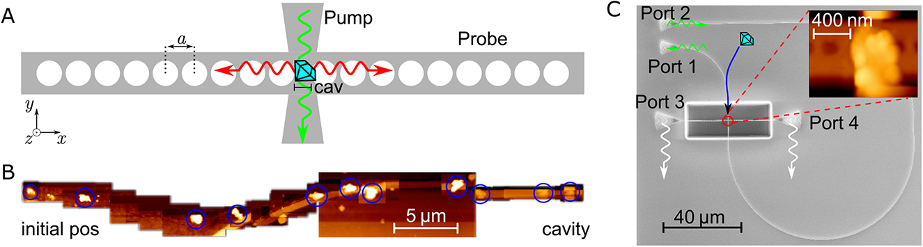
Nanopositioning of ND within cavity mode. A The periodic change a of the material on both sides of the probe waveguide lead to a photonic band gap, while the cavity is formed by the distance cav. The positioned ND can be evanescently excited through the pump waveguide. B AFM images during nanopositioning of SiV− ensemble into PCC. The distance of the initial position was approximately 40 µm to the final position on top of the cavity. C SEM image of the PCC. The device has four grating couplers – two for coupling of green light (port 1 and 2) to off-resonantly excite the emitter in the interaction zone – and two grating couplers (port 3 and 4) for collecting the emission of the cavity system. The inset shows an AFM image of the ND ensemble placed in the interaction zone.
2.2 Post-processing
The post-processing step for placing the ND within the interaction zone of the PCC follows the procedure described in Reference [14], [17]. A dispersion of NDs in water with incorporated SiV− color centers is coated on the surface of the PCC chip. Suitable SiV− center are preselected using a custom-build confocal microscope. Superimposing the confocal scan with an AFM image enables the precise localization of the SiV− center host crystal. After the preselected ND is found, the AFM cantilever tip is used to push the ND in the interaction zone of the PCC. Several steps of the positioning procedure are shown in Figure 1B. The ND is pushed along a total distance of over 40 µm.
The manipulation path is schematically drawn in the SEM image of the photonic device in Figure 1C. The positioned ND is off-resonantly excited through port 1 and its emission into the cavity-waveguide can be read out at port 3 and 4. The small inset shows an AFM image of the positioned ND in the interaction zone. A cross-talk measurement of the empty PCC probes the resonance modes. Therefore, a 532 nm laser with 0.6 mW is coupled into port 1 and the cavity signal is collected at port 3. The signal, arising from Si3N4 background fluorescence, is shown in Figure 3A (green). The occurring peaks correspond to the respective cavity modes, where the highest resonance at 721 nm shows a quality factor of Q = 2260 and the resonance near 737.4 nm has a Q-factor of Q = 1000.
2.3 Simulation of Local Density of States
The design of the freestanding PCC is numerically optimized via 3D FDTD simulations [22]. The PCC consists of two modulated Bragg mirrors with inserted cavity region in between. The periodicity of the holes (a = 265 nm) is determined to match the bandgap region of the PCC to the investigated wavelength of the SiV− ZPL. To achieve high Q-factors optimization on the cavity length and hole diameter was performed [14], [23].
For a maximum enhancement of the emitted light, the source need to be placed in the antinode of the electric field distribution of the resonance mode [24]. Thus, the position of the SiV− embedded in a ND is carried out via 3D FDTD simulations [22] in two steps. For the simulation a cube-shaped (200 nm) ND is placed on the cavity region.
The coupling strength between the optical dipole transition and the cavity field mode depends, in particular, on the dipole orientation and the position with respect to the cavity field. Both parameters can be accessed by nanomanipulation as demonstrated in reference [16] without altering the optical properties of the SiV− center. While the dipole orientation shows a cosine dependence the dipole position requires a more sophisticated study. The first optimization step is the enhancement of the Local Density of States (LDOS) dependent on the emitter position (see Figure 2A). The LDOS is proportional to the overlap integral between the electric field distribution of the resonance mode and the emitter [25]. According to the axes in Figure 1A the dipole position, embedded in a ND placed on the cavity, is centered along y- and z-direction and varied along the longitudinal x-direction, since this component shows the strongest contribution to the convolution. The rotational orientation of the dipole is aligned to the PCC axis for highest coupling. The overlap integral of the dipole and the electric field follows a cosine dependence and is therefore one for the aligned case and zero for the orthogonal orientation. The normalized LDOS enhancement is calculated for each position of the dipole with respect to the field distribution of the mode. Therefore, the enhancement of the LDOS through the cavity is divided by the LDOS enhancement for a waveguide without cavity. The highest enhancement (see Figure 2A) for odd modes is achieved for a dipole shift of ∼ (0.4–0.45) a from the symmetry plane of the center of the cavity, matching an antinode of the electric field distribution. For a reduction in simulation time, the number of segments in each Bragg-mirror was reduced to N = 18, since the electric field distribution (position of minimum and maximum) of resonance modes changes in a minor way with varying number of segments.
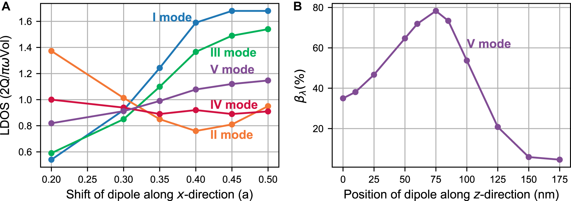
Simulation of ND position on cavity interaction zone. A Simulated LDOS enhancement for different resonance modes of the emitted light from the dipole embedded in a 200 nm cube-shaped ND, dependent on its longitudinal position weighted by the cavity periodicity a. The position of the ND is chosen according to its experimental position in Figure 1C, while the dipole position is varied along the x-direction. B Simulated on-resonance coupling efficiency
The second part of the 3D FDTD simulations targeted the position optimization of the ND embedded emitter along the z-axis. Therefore, we quantify the coupling of the emitter to the cavity with the β-factor [14], which gives the ratio of coupled spontaneous emission Γcav and the total amount of spontaneously emitted photons to free space and in the cavity Γfree + Γcav:
The
FDTD simulations are carried out to compute the Purcell enhancement [24] for the Vth-order resonance mode of the cross-bar PCCs with N = 27 and N = 53 holes, each with a 200 nm cube-shaped ND crystal on the cavity region as described above. The resulting Purcell-factors read FP = 20 and FP = 29, respectively for a spectrally and polarization matched resonance mode and an emitter located at the antinode of the electric field.
2.4 Purcell-enhanced photon emission
After the ND is positioned on top of the interaction zone, the sample is placed inside a flow-cryostat and cooled to approximately 150 K. The emitter-cavity system is excited via port 1 with 130 µW of green laser while the emission is collected through port 3 (shown in Figure 3A in orange). In blue, the free space emission of the SiV− center is shown, where the ensemble is evanescently excited through port 1 and the emission is collected at the center position of the ND. Both collection procedures are shown in the small insets in Figure 3A.
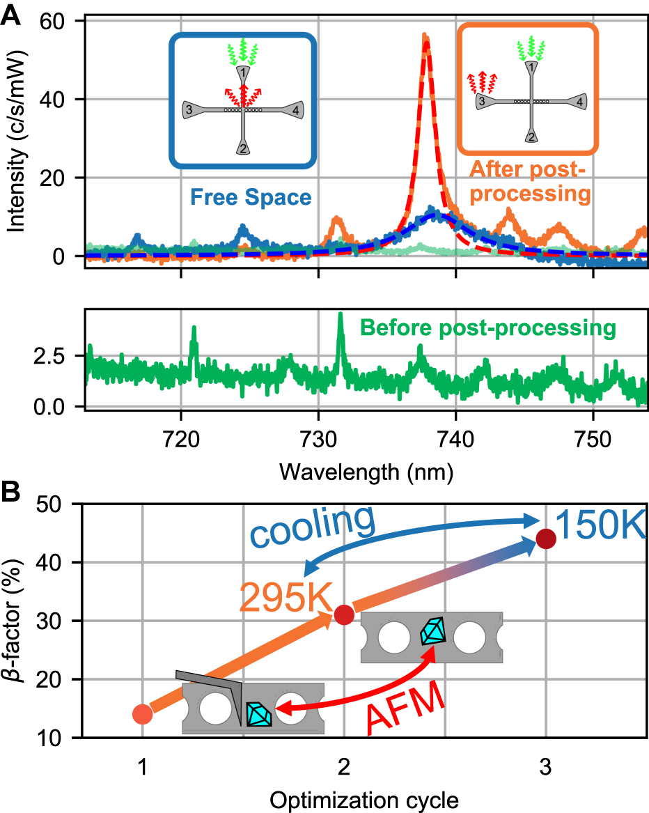
Optimized emitter-cavity coupling. A The cross-talk spectrum of the cavity (green) before the ND was placed, shows a resonance at 737.4 nm. In blue the free space emission of the SiV− ensemble for ≈150 K. The free space emission was collected in the center, while excited over port 1, as it can be seen in the small inset. The spectrum of the coupled cavity emission in orange shows a clear magnification of the emission rate for the resonance at 737.9 nm (excited over port 1 and collected from port 3). A β-factor of 0.44 corresponding to a Purcell of 0.79 was calculated from the Lorentzian fits on the free space and the cavity-emitter emission spectra. B Coupling evolution for three optimization cycles utilizing different tuning mechanism like positioning of the ND inside the interaction zone (step 1 and 2) and temperature tuning (step 3). The highest ensemble coupling was achieved for Position 2 and 150 K.
The presence of the ND in the interaction zone changes the effective refractive index of the cavity. This leads to a red shift of the desired cavity resonance. Together with a change in temperature the shift is approximately 0.4 nm. The altered mode at ∼737.9 nm of the PCC is fed by the ZPL of the SiV− ensemble. The other resonances are slightly enhanced due to phonon side band coupling and scattered background fluorescence. The Q-factor of the desired resonance decreased from Qcav = 1000 for the empty cavity to Qcoupled = 480 for the coupled system caused by scattering losses and degradation of the PCC. For obtaining the emitted photon rates we compare the photoluminescence (PL) intensities Icav, Ifree, weighted by their relative efficiencies.
According to equation (1), we obtain a coupling of:
where Ifree, Icav are the detected intensities of the free-space and cavity emission,
for all emitters inside the SiV− ensemble. The tuning mechanisms for modifying the ensemble coupling utilized so far, are position of the ND and temperature. In Figure 3B the β-factors after optimizing the position of the ND and after temperature tuning are shown. The position and orientation of the ND in the interaction zone can be controlled by AFM-based nanomanipulation [16], which yields to a better dipole alignment of the ND to the cavity axis. Position 1 and position 2 in Figure 3B correspond to a coupling averaged over the whole ensemble of 0.14 and 0.31, respectively. At position 2 we cooled the sample from 295 K to ∼150 K. This further increased the average ensemble β-factor to 0.44 (as shown in Figure 3A and given in equation (1)).
Additional reduction of the temperature to ∼4 K reveals the fine structure splitting of the SiV− centers in the ensemble. Thus, instead of the average ensemble coupling the β-factors of individual transitions of single SiV− centers can be determined, as depicted in Figure 4. Again, the free space emission (blue) needs to be compared to the joint emitter cavity signal (insets Figure 3A). Freezing and unfreezing processes, together with temperature tuning further shifted the central frequency of the resonance mode to approximately 740.3 nm (depicted in gray Figure 4 top). This implies a detuning from the average ensemble ZPL resonance at ∼738 nm leading to decreased average coupling. The detuning enables the coupling of individual, however more strained, SiV− centers (Figure 4 top), apparent when zooming into the red square (Figure 4 bottom). A splitting of (244 ± 10) GHz between the doublet of (A,B) and (C,D) is observed, while the splitting between C and D is (37 ± 10) GHz. These four lines arise from one SiV− center with an excited state splitting of 252 GHz and a ground state splitting of 46.3 GHz influenced by the strain inside the ND [4], where the ZPL position of the SiV− can be shifted (axial strain) while keeping the state splitting constant (low transverse strain) [27]. The used NDs have proven to inhere low transverse strain [4]. For the SiV− center transition A and D have the same dipole orientation as well as transition B and C [28]. Figure 4 confirms that transition B and C show a better coupling to the cavity mode than transition A and D originating from dipole alignment of the emitter to the cavity axis. Due to strain induced differences in the selection rules, transition B and C show different enhancement factors [29].
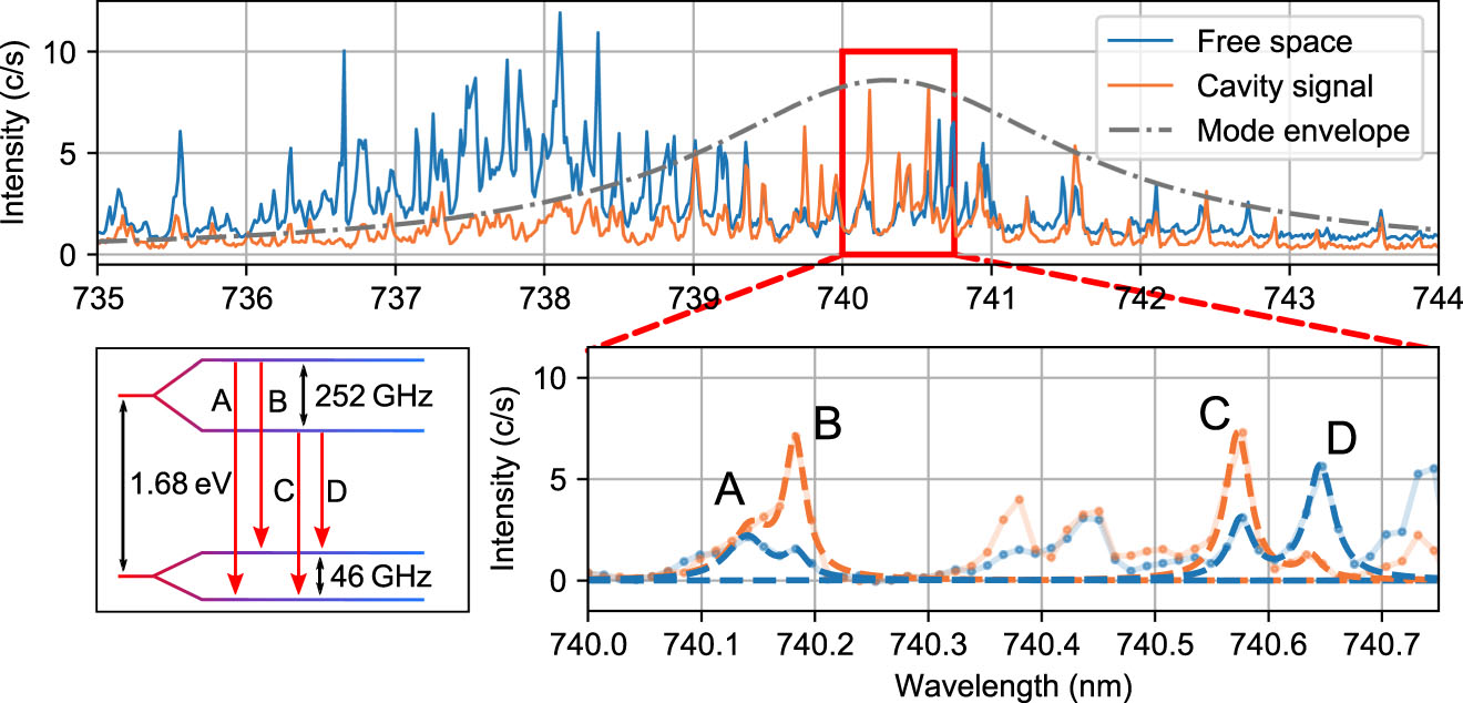
Spectrum of coupled emitter-cavity system at cryogenic temperatures. Cavity emission of coupled SiV− ensemble in orange. Free space emission in blue and envelope resonance mode in gray. For some spectral lines, the emission into the cavity mode reaches higher counting rates than into free space. The lower plot shows a zoom of the area in the red rectangle and the four transitions A–D (level scheme sketched on the right) of the SiV− center are referenced to the lines according to their spacing.
Similar dipole orientation of the transitions reach higher (B and C) and lower (A and D) coupling efficiencies to the cavity mode. From these values according to equation (1), we estimate the β-factor for all four transitions. The highest coupling was achieved for transition B, which is
4/5 of the total spontaneous emission are channeled into the photonic circuit. The measured β-factor of 0.81 corresponds to a lifetime reduction of
3 Outlook
In our work we demonstrate the efficient coupling of individual optical transitions of SiV− centers to a Si3N4-based cross-bar PCC with a Purcell enhancement of more than 4, where the enhanced signal was read out via a probe waveguide (with a PCC) by excitation via a crossed waveguide on chip. Much higher Purcell enhancement is prohibited by residual scattering from the ND reducing the overall Q-factor of the PCC. Furthermore, the achievable evanescent coupling strength is ultimately limited by the distance of the SiV− center to the field maximum of the PCC. In future experiments we envision Purcell factors beyond 100 for single SiV− center in NDs with diameter of a few ten nanometers. To emphasize the influence of the ND emitter host on the Purcell enhancement factor simulations without the scattering crystal were computed leading to FP = 68 (
4 Methods
4.1 Fabrication of nanodiamonds
SiV− containing diamond nanoparticles were obtained by HPHT treatment of the metal catalysts-free growth system based on a homogeneous mixture of naphthalene (C10H8), fluorographite (CF1.1), and tetrakis(trimethylsilyl)silane (C12H36Si5) which was used as the Si doping component. (Introduction of fluorine-containing compounds into the growth system was intended to reduce the content of NV centers in NDs-SiV−) HPHT treatment of the initial homogeneous mixtures was carried out in a high-pressure apparatus of “Toroid” type. The experimental procedure consists of loading the high-pressure apparatus to 8.0 GPa, heating the samples up to 1450 °C and short (3 s) isothermal exposures at these temperatures.
4.2 Fabrication of the photonic chip
Free-standing PCC devices on chip were realized on Silicon nitride-on-insulator wafers consisting of 200 nm stoichiometric Si3N4 on top of a 2 µm thick SiO2 layer on top of Si. Fabrication of the nanophotonic circuits involved several steps of electron-beam lithography (e-beam) followed by reactive ion etching. The nanophotonic circuits were defined on top of the Si3N4 layer using negative tone photoresist ma-N 2403 in the first lithography step and after were 75% dry-etched into the silicon nitride layer using an CHF3/O2 plasma. To realize freestanding PCC underneath SiO2 should be removed, which was achieved by opening a window around the photonic crystal region in the second step of lithography by means of exposing positive photoresist PMMA in this area. In the following step, the remaining 25% of silicon nitride in the window area was etched, while the waveguide inside of the window was protected with a ma-N 2403 photoresist; the waveguides outside the windows were protected by unexposed PMMA photoresist. After that, both photoresists were removed by O2 plasma. In the last fabrication step SiO2 layer in the windows was removed by wet etching, namely by immersing the chip in hydrofluoric acid (HF).
4.3 Optical methods
The optical readout was established by a self build confocal microscope setup with an NA = 0.55 objective (×50 magnification). For scanning the sample, a galvo mirror system was used. With the help of a second laser path and a 4f-lens system, the laser can be set on a fixed position, while the readout is collected from a different position. The readout can be directed on a spectrometer and an avalanche photo diode.
Funding source: Verein Deutscher Ingenieure, Germany
Funding source: Russian Foundation for Basic Research, Russia, Germany
Award Identifier / Grant number: 18-03-00936
Funding source: Deutsche Forschungsgemeinschaft
Award Identifier / Grant number: 398628099
Acknowledgment
The project was funded by the Deutsche Forschungsgemeinschaft (DFG, German Research Foundation) – Project number: 398628099. AK acknowledges support of the BMBF/VDI in project Q.Link.X and the European fund for regional development (EFRE) program Baden-Württemberg. KGF and AK acknowledge support of IQst. The AFM was funded by the DFG. We thank Prof. Kay Gottschalk and Frederike Erb for their support. V. A. Davydov thanks the Russian Foundation for Basic Research (Grant No. 18-03-00936) for financial support.
Author contribution: All the authors have accepted responsibility for the entire content of this submitted manuscript and approved submission.
Conflict of interest statement: The authors declare no conflicts of interest regarding this article.
References
[1] M. Atatüre, D. Englund, N. Vamivakas, S.-Y. Lee, and J. Wrachtrup, “Material platforms for spin-based photonic quantum technologies,” Nat. Rev. Mater., vol. 3, pp. 38–51, 2018. https://doi.org/10.1038/s41578-018-0008-9.Suche in Google Scholar
[2] D. D. Awschalom, R. Hanson, J. Wrachtrup, and B. B. Zhou, “Quantum technologies with optically interfaced solid-state spins,” Nat. Photonics, vol. 12, pp. 516–527, 2018. https://doi.org/10.1038/s41566-018-0232-2.Suche in Google Scholar
[3] J. N. Becker and C. Becher, “Coherence properties and quantum control of silicon vacancy color centers in diamond,” Phys. Status Solidi A, vol. 214, p. 1700586, 2017. https://doi.org/10.1002/pssa.201700586.Suche in Google Scholar
[4] L. J. Rogers, O. Wang, Y. Liu, et al., “Single Si-V− centers in low-strain nanodiamonds with bulklike spectral properties and nanomanipulation capabilities,” Phys. Rev. Appl., vol. 11, 2019, Art no. 024073. https://doi.org/10.1103/physrevapplied.11.024073.Suche in Google Scholar
[5] A. Sipahigil, K. D. Jahnke, L. J. Rogers, et al., “Indistinguishable photons from separated silicon-vacancy centers in diamond,” Phys. Rev. Lett., vol. 113, p. 113602, 2014. https://doi.org/10.1103/physrevlett.113.113602.Suche in Google Scholar
[6] Y.-I. Sohn, S. Meesala, B. Pingault, et al., “Controlling the coherence of a diamond spin qubit through its strain environment,” Nat. Commun., vol. 9, no. 1, pp. 1–6, 2018. https://doi.org/10.1038/s41467-018-04340-3.Suche in Google Scholar PubMed PubMed Central
[7] D. D. Sukachev, A. Sipahigil, C. T. Nguyen, et al., “Silicon-vacancy spin qubit in diamond: a quantum memory exceeding 10 ms with single-shot state readout,” Phys. Rev. Lett., vol. 119, no. 22, p. 223602, 2017. https://doi.org/10.1103/physrevlett.119.223602.Suche in Google Scholar PubMed
[8] M. H. Metsch, K. Senkalla, B. Tratzmiller, et al., “Initialization and readout of nuclear spins via a negatively charged silicon-vacancy center in diamond,” Phys. Rev. Lett., vol. 122, no. 19, p. 190503, 2019. https://doi.org/10.1103/physrevlett.122.190503.Suche in Google Scholar
[9] K.-M. C. Fu, C. Santori, P. E. Barclay, et al., “Coupling of nitrogen-vacancy centers in diamond to a gap waveguide,” Appl. Phys. Lett., vol. 93, p. 234107, 2008. https://doi.org/10.1063/1.3045950.Suche in Google Scholar
[10] D. Englund, B. Shields, K. Rivoire, et al., “Deterministic coupling of a single nitrogen vacancy center to a photonic crystal cavity,” Nano Lett., vol. 10, pp. 3922–3926, 2010. https://doi.org/10.1021/nl101662v.Suche in Google Scholar PubMed
[11] P. E. Barclay, K.-M. C. Fu, C. Santori, A. Faraon, and R. G. Beausoleil, “Hybrid nanocavity resonant enhancement of color center emission in diamond,” Phys. Rev. X, vol. 1, 2011, Art no. 011007. https://doi.org/10.1103/physrevx.1.011007.Suche in Google Scholar
[12] J. Wolters, A. W. Schell, G. Kewes, et al., “Enhancement of the zero phonon line emission from a single nitrogen vacancy center in a nanodiamond via coupling to a photonic crystal cavity,” Appl. Phys. Lett., vol. 97, p. 141108, 2010. https://doi.org/10.1063/1.3499300.Suche in Google Scholar
[13] M. Radulaski, J. L. Zhang, Y.-K. Tzeng, et al., “Nanodiamond integration with photonic devices,” Laser Photonics Rev., vol. 13, no. 8, p. 1800316, 2019. https://doi.org/10.1002/lpor.201800316.Suche in Google Scholar
[14] K. G. Fehler, A. P. Ovvyan, N. Gruhler, W. H. P. Pernice, and A. Kubanek, “Efficient coupling of an ensemble of nitrogen vacancy center to the mode of a high-Q, Si3N4 photonic crystal cavity,” ACS Nano, vol. 13, pp. 6891–6898, 2019. https://doi.org/10.1021/acsnano.9b01668.Suche in Google Scholar PubMed
[15] U. Jantzen, A. B. Kurz, D. S. Rudnicki, et al., “Nanodiamonds carrying silicon-vacancy quantum emitters with almost lifetime-limited linewidths,” New J. Phys., vol. 18, 2016, Art no. 073036. https://doi.org/10.1088/1367-2630/18/7/073036.Suche in Google Scholar
[16] S. Häußler, L. Hartung, K. G. Fehler, et al., “Preparing single SiV− center in nanodiamonds for external, optical coupling with access to all degrees of freedom,” New J. Phys., vol. 21, p. 103047, 2019. https://doi.org/10.1088/1367-2630/ab4cf7.Suche in Google Scholar
[17] A. W. Schell, G. Kewes, T. Schröder, J. Wolters, T. Aichele, and O. Benson, “A scanning probe-based pick-and-place procedure for assembly of integrated quantum optical hybrid devices,” Rev. Sci. Instrum., vol. 82, 2011, Art no. 073709. https://doi.org/10.1063/1.3615629.Suche in Google Scholar PubMed
[18] S. Wehner, D. Elkouss, and R. Hanson, “Quantum internet: A vision for the road ahead,” Science, vol. 362, no. 6412, 2018, Art no. eaam9288. https://doi.org/10.1126/science.aam9288.Suche in Google Scholar PubMed
[19] J. B. Spring, B. J. Metcalf, P. C. Humphreys, et al., “Boson sampling on a photonic chip,” Science, vol. 339, pp. 798–801, 2013. https://doi.org/10.1126/science.1231692.Suche in Google Scholar PubMed
[20] K. Li, Y. Zhou, A. Rasmita, I. Aharonovich, and W. Gao, “Nonblinking emitters with nearly lifetime-limited linewidths in cvd nanodiamonds,” Phys. Rev. Appl., vol. 6, no. 2, 2016, Art no. 024010. https://doi.org/10.1103/physrevapplied.6.024010.Suche in Google Scholar
[21] Y. Zhou, A. Rasmita, K. Li, Q. Xiong, I. Aharonovich, and W.-b. Gao, “Coherent control of a strongly driven silicon vacancy optical transition in diamond,” Nat. Commun., vol. 8, no. 1, pp. 1–7, 2017. https://doi.org/10.1038/ncomms14451.Suche in Google Scholar PubMed PubMed Central
[22] A. F. Oskooi, D. Roundy, M. Ibanescu, P. Bermel, J. D. Joannopoulos, and S. G. Johnson, “Meep: A flexible free-software package for electromagnetic simulations by the fdtd method,” Comput. Phys. Commun., vol. 181, pp. 687–702, 2010. https://doi.org/10.1016/j.cpc.2009.11.008.Suche in Google Scholar
[23] Y. Akahane, T. Asano, B.-S. Song, and S. Noda, “High-q photonic nanocavity in a two-dimensional photonic crystal,” Nature, vol. 425, p. 944, 2003. https://doi.org/10.1038/nature02063.Suche in Google Scholar PubMed
[24] E. M. Purcell, H. C. Torrey, and R. V. Pound, “Resonance absorption by nuclear magnetic moments in a solid,” Phys. Rev., vol. 69, p. 37, 1946. https://doi.org/10.1103/physrev.69.37.Suche in Google Scholar
[25] A. Taflove, A. Oskooi, and S. G. Johnson, Advances in FDTD Computational Electrodynamics: Photonics and Nanotechnology, Artech House, 2013.Suche in Google Scholar
[26] J. L. Zhang, S. Sun, M. J. Burek, et al., “Strongly cavity-enhanced spontaneous emission from silicon-vacancy centers in diamond,” Nano Lett., vol. 18, pp. 1360–1365, 2018. https://doi.org/10.1021/acs.nanolett.7b05075.Suche in Google Scholar PubMed
[27] S. Meesala, Y.-I. Sohn, B. Pingault, et al., “Strain engineering of the silicon-vacancy center in diamond,” Phys. Rev. B, vol. 97, no. 20, p. 205444, 2018. https://doi.org/10.1103/physrevb.97.205444.Suche in Google Scholar
[28] L. J. Rogers, K. D. Jahnke, M. H. Metsch, et al., “All-optical initialization, readout, and coherent preparation of single silicon-vacancy spins in diamond,” Phys. Rev. Lett., vol. 113, p. 263602, 2014. https://doi.org/10.1103/physrevlett.113.263602.Suche in Google Scholar PubMed
[29] C. Hepp, T. Müller, V. Waselowski, et al., “Electronic structure of the silicon vacancy color center in diamond,” Phys. Rev. Lett., vol. 112, no. 3, 2014, Art no. 036405. https://doi.org/10.1103/physrevlett.112.036405.Suche in Google Scholar
[30] A. Imamoglu, D. D. Awschalom, G. Burkard, et al., “Quantum information processing using quantum dot spins and cavity qed,” Phys. Rev. Lett., vol. 83, pp. 4204–4207, 1999. https://doi.org/10.1103/PhysRevLett.83.4204.Suche in Google Scholar
[31] M. J. Kastoryano, F. Reiter, and A. S. Sørensen, “Dissipative preparation of entanglement in optical cavities,” Phys. Rev. Lett., vol. 106, 2011, Art no. 090502. https://doi.org/10.1103/physrevlett.106.090502.Suche in Google Scholar
[32] S.-B. Zheng and G.-C. Guo, “Efficient scheme for two-atom entanglement and quantum information processing in cavity qed,” Phys. Rev. Lett., vol. 85, pp. 2392–2395, 2000. https://doi.org/10.1103/physrevlett.85.2392.Suche in Google Scholar PubMed
[33] E. Waks and J. Vuckovic, “Dipole induced transparency in drop-filter cavity-waveguide systems,” Phys. Rev. Lett., vol. 96, p. 153601, 2006. https://doi.org/10.1103/physrevlett.96.153601.Suche in Google Scholar
[34] J. Borregaard, P. Kómár, E. M. Kessler, M. D. Lukin, and A. S. Sørensen, “Long-distance entanglement distribution using individual atoms in optical cavities,” Phys. Rev. A, vol. 92, 2015, Art no. 012307. https://doi.org/10.1103/physreva.92.012307.Suche in Google Scholar
[35] J. I. Cirac, P. Zoller, H. J. Kimble, and H. Mabuchi, “Quantum state transfer and entanglement distribution among distant nodes in a quantum network,” Phys. Rev. Lett., vol. 78, pp. 3221–3224, 1997. https://doi.org/10.1103/physrevlett.78.3221.Suche in Google Scholar
[36] P. Kok, W. J. Munro, K. Nemoto, T. C. Ralph, J. P. Dowling, and G. J. Milburn, “Linear optical quantum computing with photonic qubits,” Rev. Mod. Phys., vol. 79, p. 135, 2007. https://doi.org/10.1103/revmodphys.79.135.Suche in Google Scholar
[37] H. Riedmatten and M. Afzelius, Quantum Light Storage in Solid State Atomic Ensembles. Nano-Optics and Nanophotonics, Springer International Publishing, 2015.10.1007/978-3-319-19231-4_9Suche in Google Scholar
[38] W. J. Munro, K. Azuma, K. Tamaki, and K. Nemoto, “Inside quantum repeaters,” IEEE J. Sel. Top. Quantum Electron, vol. 21, pp. 78–90, 2015. https://doi.org/10.1109/jstqe.2015.2392076.Suche in Google Scholar
[39] B. M. Terhal, “Quantum error correction for quantum memories,” Rev. Mod. Phys., vol. 87, pp. 307–346, 2015. https://doi.org/10.1103/revmodphys.87.307.Suche in Google Scholar
[40] C. L. Degen, F. Reinhard, and P. Cappellaro, “Quantum sensing,” Rev. Mod. Phys., vol. 89, 2017, Art no. 035002. https://doi.org/10.1103/revmodphys.89.035002.Suche in Google Scholar
© 2020 Konstantin G. Fehler et al., published by De Gruyter, Berlin/Boston
This work is licensed under the Creative Commons Attribution 4.0 International License.
Artikel in diesem Heft
- Reviews
- Boron nitride for excitonics, nano photonics, and quantum technologies
- Design for quality: reconfigurable flat optics based on active metasurfaces
- Research Articles
- Microwave oscillator and frequency comb in a silicon optomechanical cavity with a full phononic bandgap
- Second harmonic generation in metasurfaces with multipole resonant coupling
- Symmetry-tailored patterns and polarizations of single-photon emission
- Highly transparent and conductive metal oxide/metal/polymer composite electrodes for high-efficiency flexible organic light-emitting devices
- Optical anapole mode in nanostructured lithium niobate for enhancing second harmonic generation
- Temporal plasmonics: Fano and Rabi regimes in the time domain in metal nanostructures
- Chemiluminescent carbon nanodots as sensors for hydrogen peroxide and glucose
- Dual-polarized multiplexed meta-holograms utilizing coding metasurface
- Tunable photoluminescence properties of selenium nanoparticles: biogenic versus chemogenic synthesis
- Compact disordered magnetic resonators designed by simulated annealing algorithm
- Controlling the plasmon resonance via epsilon-near-zero multilayer metamaterials
- 2D GeP-based photonic device for near-infrared and mid-infrared ultrafast photonics
- Purcell-enhanced emission from individual SiV− center in nanodiamonds coupled to a Si3N4-based, photonic crystal cavity
- Ultrasensitive and fast photoresponse in graphene/silicon-on-insulator hybrid structure by manipulating the photogating effect
- Multiresonant plasmonic nanostructure for ultrasensitive fluorescence biosensing
- Advanced encryption method realized by secret shared phase encoding scheme using a multi-wavelength metasurface