A flexible platform for controlled optical and electrical effects in tailored plasmonic break junctions
-
Florian Laible

 ,
Kai Braun
,
Otto Hauler
,
Kai Braun
,
Otto Hauler

Abstract
Mechanically controllable break junctions are one suitable approach to generate atomic point contacts and ultrasmall and controllable gaps between two metal contacts. For constant bias voltages, the tunneling current can be used as a ruler to evaluate the distance between the contacts in the sub-1-nm regime and with sub-Å precision. This ruler can be used to measure the distance between two plasmonic nanostructures located at the designated breaking point of the break junction. In this work, an experimental setup together with suitable nanofabricated break junctions is developed that enables us to perform simultaneous gap-dependent optical and electrical characterization of coupled plasmonic particles, more specifically bowtie antennas in the highly interesting gap range from few nanometers down to zero gap width. The plasmonic break junction experiment is performed in the focus of a confocal microscope. Confocal scanning images and current measurements are simultaneously recorded and exhibit an increased current when the laser is focused in the proximity of the junction. This setup offers a flexible platform for further correlated optoelectronic investigations of coupled antennas or junctions bridged by nanomaterials.
1 Introduction
Mechanically controllable break junctions (MCBJs) are primarily used for investigations of the electrical properties of molecules for molecular electronics [1] and metal point contacts [2]. The concept of a break junction is well known since 1985 [3]. Starting from there, they were continuously refined and advanced to perform under ambient conditions. Mechanically controllable break junctions are usually fabricated by thinning a wire either by chemical etching [4] or electromigration [5]. A different approach is to lithographically predefine a wire with a designated breaking point [6]. By introducing mechanical stress, the junctions break at their weakest point. During the breaking process, the conductance of an MCBJ gradually decreases, showing quantized conductance in multiples of the (spin-degenerate) conductance quantum G0=2e2/h when the current is transported by few down to single atoms [7], where G0 represents the conductance of an atomic point contact [8], [9]. After the last atom connecting the two sides has lost physical contact, charge transfer takes place until the contacts are separated by more than approximately 1 nm, and the tunneling current drops below the detection limit. With a sufficiently small and static bias, the tunnel current can be used as a ruler with sub-Å precision [10]. This effect is also exploited in scanning tunneling microscopy [11]. The small gaps between the metal contacts induce high electrical near-fields when excited. This has been used for surface-enhanced Raman spectroscopy (SERS) of molecules in the gap of a break junction [12]. Optical experiments with break junctions have revealed an increased tunneling current when the junction is illuminated with laser light [13], [14]. Also, experiments on the transmission of surface plasmon polaritons through atomic point contacts and break junctions with ultranarrow gaps have been performed in the past [15], [16].
As another aspect of nanogap investigations, the coupling of plasmonic nanoantennas across ultranarrow gaps has proven to be of high interest. As nanoantennas metallic, most commonly gold, nanoparticles are used. Plasmons are collective oscillations of the free electron density at a metal–dielectric interface. If the metal particle is smaller than the wavelength of visible light, a collective oscillation of the free electron gas within the particle can be excited. These excitations are called localized surface plasmon polaritons (LSPPs). The collective motion of the electrons results in an accumulation of charge at the edges of the particle, which causes an enhanced electrical near-field around the antenna, especially under resonant conditions [17]. The frequency of the LSPP resonance depends on the material and shape of the particle, the refractive index of the media surrounding it, and the presence of other particles in the proximity of the antenna [18].
If two nanoantennas are positioned in close proximity to each other (separated by less than roughly the radius of one antenna), the near-fields of both nanoantennas couple, leading to a dimer configuration. In this work, we look at dimers consisting of two equally sized triangles that are pointing at each other. This antenna configuration is called a bowtie (BT). The modes of the antennas along the long axis of the dimer hybridize, resulting in a longitudinal bonding- and antibonding mode. For the bonding mode, the surface charge density near the gap is heteropolar and for the antibonding mode homopolar [19]. With decreasing distance, the hybridization increases. This leads to a red shift of the bonding mode and a blue shift of the antibonding mode, as well as a strong increase of the near-field in the gap at the wavelength of the bonding mode [20], [21].
This behavior changes when the distance between the nanoantennas is small enough for electrons to tunnel through the gap. These ultranarrow gaps are generally very difficult to fabricate and control. By introducing plasmonic nanoantennas into MCBJs, the device can be used as a test bench for dimers with sub-1-nm gap sizes to investigate the coupling in the transition from the classical [19], [22] to the quantum mechanical regime [23].
The integration of the BTs also opens up several other possibilities, such as using the plasmonic antennas to further enhance the Raman signal in the gap area, making the MCBJs even more potent in this field. Alternatively, by bridging the gap, conductance measurements can be performed on nanomaterials or single molecules [24], [25], [26], [27]. In the present work, BT-shaped plasmonic MCBJs are broken by bending in the focus of a confocal microscope. This enables combined in situ measurements of tunneling current, and therefore gap width, and the localized plasmonic resonance of the BT before and after breaking, as well as the scattering and luminescence of the plasmonic dimer particle.
2 Results
2.1 Sample design
As the design of the MCBJs, connected gold BTs with a designated breaking point at the center are chosen. Constrictions between the BT and contact lines partially decouple the plasmonic structures from the leads. The MCBJ is elevated on a plateau above the substrate and underetched to improve the breaking performance. The substrate consists of bendable thin steel sheet plates that are coated with a layer of polyimide (PI). The PI layer acts as an insulation layer and smoothens the relatively rough steel surface. The fabrication of the plasmonic break junctions consists of the substrate preparation and two lithography steps followed by reactive ion etching (RIE). A several-millimeters-long lead with a designated breaking point at the connection between two nanotriangles is fabricated on the PI film via electron beam lithography. The width of the designated breaking point located in the middle of the lead is 10 to 50 nm. In the broken state, the triangles are forming a BT nanoantenna. The triangles are connected to leads at their bases. To decouple the nanoantenna from the leads, the contact point is much smaller than the base of the triangle, but wider than the designated breaking point. The PI is partially etched away until the breaking point is freestanding to promote the breaking of the junction. In order to excite localized plasmonic oscillations of the free electron gas of the BT dimer, the particles must be smaller than the wavelength of the exciting light. Therefore, the plasmonic particles must be as much as possible decoupled from the leads.
Two approaches for the decoupling are shown in Figure 1. Introducing bottlenecks before and after the BT is the first approach (Figure 1A and C). The constrictions partly separate the gold BT from the gold leads. Localized surface plasmon polaritons can form along the long axis of the BT, but some charge carriers will propagate through the bottleneck away from the BT. To reduce this effect, the leads can be tilted by 45° (Figure 1D). If the polarization of the exciting light is oriented perpendicular to the leads, the leakage of the plasmons is minimized, and the coupling peak can best be monitored. The plasmonic nanoparticle at the designated breaking point of the junctions sets these samples apart from classical break junctions. This configuration opens the field for a vast variety of experiments and introduces a new analysis channel into MCBJs. Investigations of ultranarrow gap dimers become possible, as well as correlative SERS and conductance measurements.
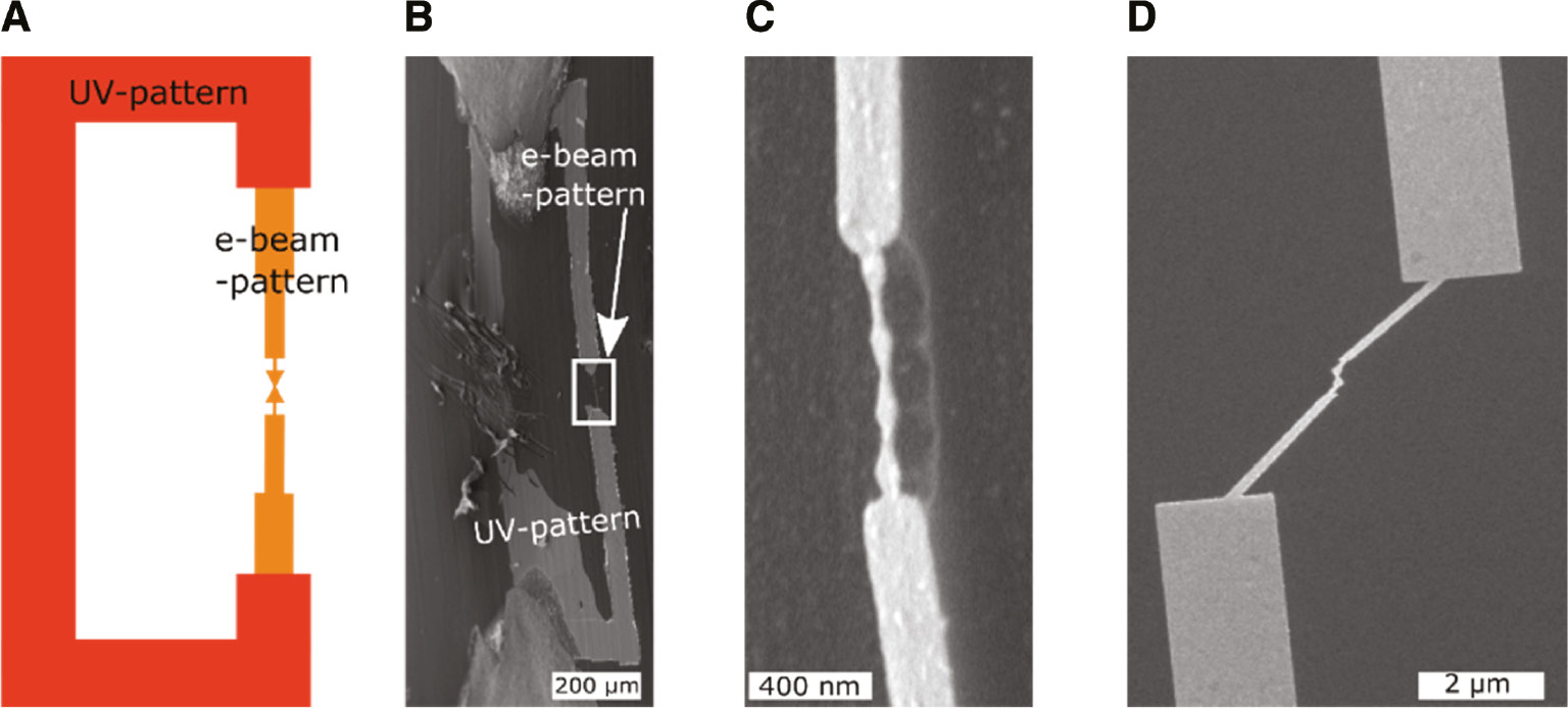
Overview of the fabricated geometries and patterns.
(A) Layout of the exposure pattern. The UV pattern is formed as a horseshoe in order to shortcut the MCBJ and therefore protect the junction from electrostatic damage in the following fabrication steps and mounting process. (B) Scanning electron microscope image of the UV pattern and the e-beam patterns. The UV structure is contacted with conducting silver on both sides of the MCBJ and then scratched through, removing the shortcut. (C) Side view of the elevated BT region after the RIE step. The bottlenecks above and below the BT partially decouple the BT from the leads. (D) Mechanically controllable break junction design with angled contact lines, further decoupling the BT from the contact lines.
2.2 Excitation of LSPPs in integrated BT nanoantennas
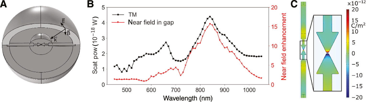
In order to verify that it is possible to excite localized plasmon polaritons in a BT that is integrated in a break junction, finite element method simulations are performed using COMSOL Multiphysics. The applied model is shown in Figure 2A. The exciting electromagnetic wave is transverse magnetically (TM) polarized, i.e. the electric field is oriented perpendicularly to the wave vector and lies in the plane of incidence. The wave vector
Finite element method simulation of a plasmonic MCBJ.
(A) Simulation model of a plasmonic break junction. The gap of the integrated BT is set to 6 nm. The base of the BT measures 120 nm, and the length of the triangle is 130 nm. (B) Simulated spectra of the scattered power (black squares) and the near-field enhancement in the gap (red triangles). The exciting light is TM polarized. The electric field is oriented along the long axis of the BT. (C) Surface charge density near the plasmonic break junction. The wavelength of the exciting light is chosen to 840 nm. The charge distribution implies that the main peak in (B) can be attributed to the bonding mode of the BT.
2.3 Bending device
A three-point bending device is engineered to fit on an existing inverse confocal microscope. In this setup, the junction is pointing downward. In contrast to most other known bending devices for MCBJs, all three points are adjustable in the z-direction (Figure 3). While the central pusher is driven by a screw, the outer fixating points are spring loaded against the micrometer screws from the top. The sample is mounted on the bending device. The springs at the outer points are fully compressed (Figure 3A). The sample is then bent until the conductance of the junction is starting to measurably decrease. Now the objective of the confocal microscope is moved up until the junction is in focus (Figure 3B). The bending of the sample is now increased by slowly releasing the outer screws while the sample stays mostly in focus (Figure 3C). A schematic of the whole setup and individual components is shown in Figure 3D.
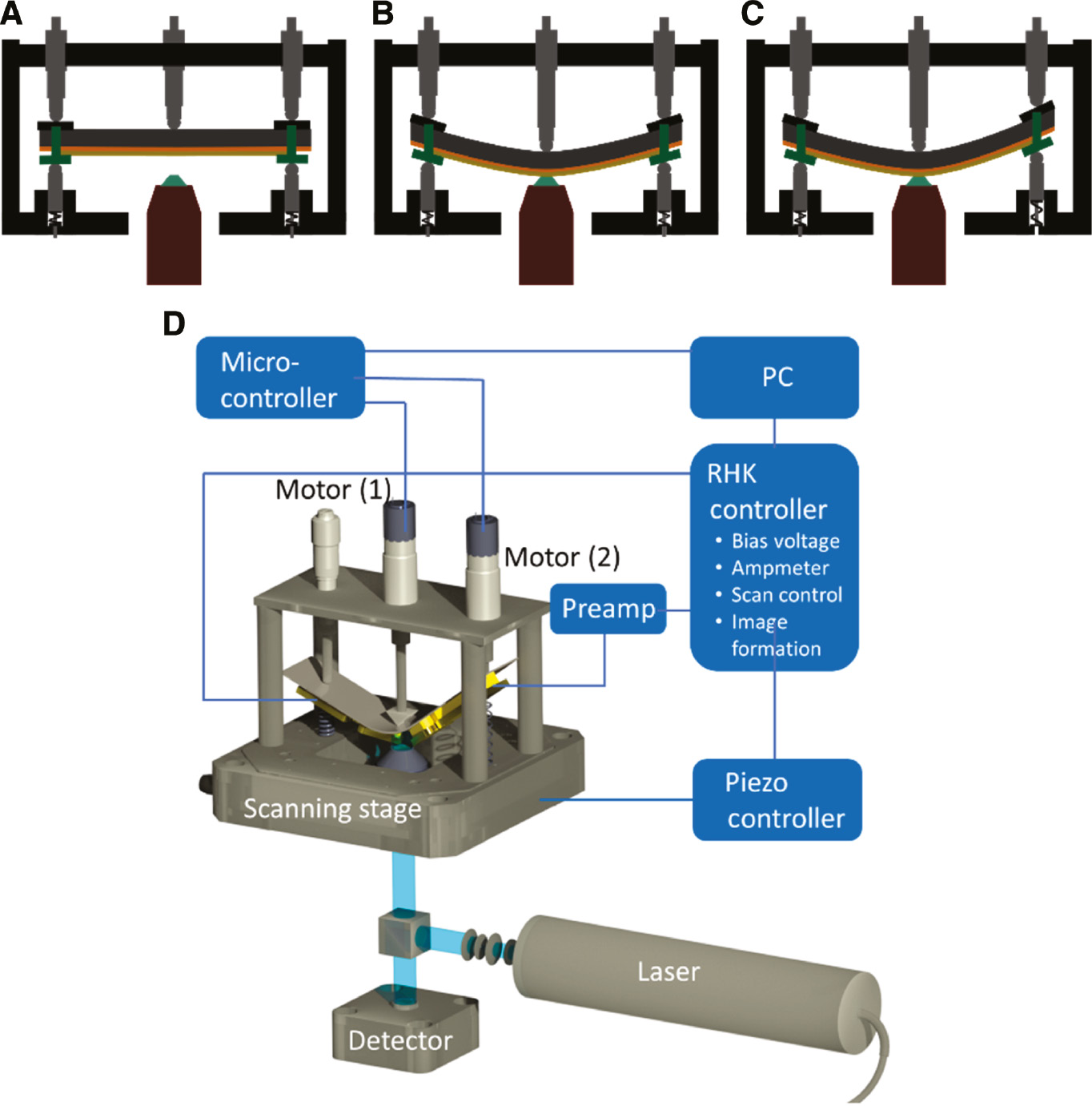
Schematic of the three-point bending device.
(A) Starting position. (B) Initial deformation via the central pusher. The sample is in the focus of the objective. (C) Additional bending via releasing one outer screw. The sample stays in focus. (D) Schematic of the combined bending and measurement setup with the relevant components.
2.4 Electrical measurements
The breaking process is monitored via an ammeter (see Section 4). The sample is prebent with the center pusher until the current begins to drop. Then, one of the counter supports is moved upward by a motor with a speed of 150 μm/min. The current is measured at 100 times per second. The conductance is evaluated with G0 as the unit. An exemplary conductance-over-time measurement is shown in Figure 4A. The data from Figure 4A are plotted as a histogram in Figure 4B, showing increased occurrences of values at or near integer multiples of G0 [28], [29], [30]. Such a quantized decrease of the conductance is expected for break junctions. In experiments dedicated to the quantification of G0, the bending and breaking are done more slowly and repeated several times by opening and closing the junction during the measurement. This results in increased statistics for the conductance histograms. Here, the measurement shown in Figure 4A and B clearly illustrates the finite steps in the conductance during the breaking process of the MCBJ resulting from the quantized conductance.
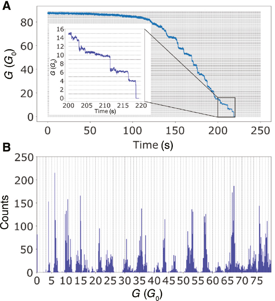
Results of electrical measurements during the breaking process of an MCBJ.
(A) Conductance measurement of an MCBJ over time. The junction was manually prebent. The bending is controlled by one continuously moving motor at one of the outer screws. Quantized conductance is observable. The last measured conductance step in this case is 4 G0. (B) Histogram of the data points of the plot in (A) showing accumulations near multiples of G0.
Each step represents one or several transport channels that are no longer participating in the charge transport. This measurement proves that the gold contact is breaking apart, and the loss of conduction does not have any other causes. To verify that the lead indeed breaks at the designated breaking point, the samples are heavily bent and examined with a scanning electron microscope (SEM) before and after the electrical and optical measurements (Figure 5A and B). One can clearly see the narrow gap in Figure 5B created at the previously connected BT center.

SEM images of a plasmonic MCBJ before and after bending the substrate.
(A) Connected plasmonic BT break junction after fabrication. (B) Plasmonic break junction that was broken at the designated breaking point exhibiting a nanogap after bending.
Important factors to control stable gap widths are, for example, the rotation speed of the motor that controls the bending, as well as the thickness of the PI. This thickness alters the gearing, that is, the ratio between the displacement of the pusher and corresponding gap displacement [2]. In the broken state, the MCBJs are relatively stable at a gap width of ~0.4 nm. Once this gap width is reached, the current through the MCBJ can be stabilized for up to minutes. The current here amounts to 4 nA at a bias voltage of 50 mV. For even narrower gaps, several processes may take place that can lead to dynamic modifications, such as thermal mobility of the gold atoms and electromigration [31], [32], or local modification of the junction, for example, by attraction of contaminants to high field regions. For lower currents, the MCBJs tend to drift apart. For higher currents, they tend to close up. To obtain time slots with stable currents in the tunneling regime, the motor at the counter support is used to stabilize the current at a given value in a feedback loop. Therefore, the current is measured, and the motor moves up or down, depending on whether the current is higher or lower than the target value. In Figure 6, a measurement is shown where the target current is 0.5 nA. The motor motion and its direction are illustrated, indicating whether the motor moves downward, thus decreasing the bending of the sample, or is moving upward, increasing the curvature of the sample. At the beginning of the measurement, the MCBJ is open, and no tunneling current can be observed. After decreasing the bending of the sample for 100 s, the current rises quickly into the overload of the preamplifier. The motor changes direction, and the current drops again to 0 A. This process repeats itself one more time. Then, the current can be stabilized around the target current for 20 s. During this time, optical measurements can be carried out. After the stable period, the current drops to zero, and the measurement ends.

Current measurement of an MCBJ with a gap.
The microcontroller is set to stabilize the current at 0.5 nA. In green areas, the motor is releasing the substrate; in red areas, the bending angle is increased. In white areas, the motor is stopped.
2.5 Combined electrical and optical measurements with a 488-nm irradiation
As discussed in the previous section, the MCBJs in their broken state are relatively stable at gaps of 0.4 nm. For the correlative measurements, an MCBJ is broken and mechanically tuned until the tunneling current is stabilized. The MCBJ is brought into the focus of a 488-nm continuous-wave (CW) laser (see Section 4). The light is linearly polarized, and the polarization axis is oriented parallel to the y axis of the scan window, that is, roughly parallel to the long axis of the BT (Figure 7A and D). The laser power is set to 50 μW. The energy density on the sample is 49.5 kW/cm2.
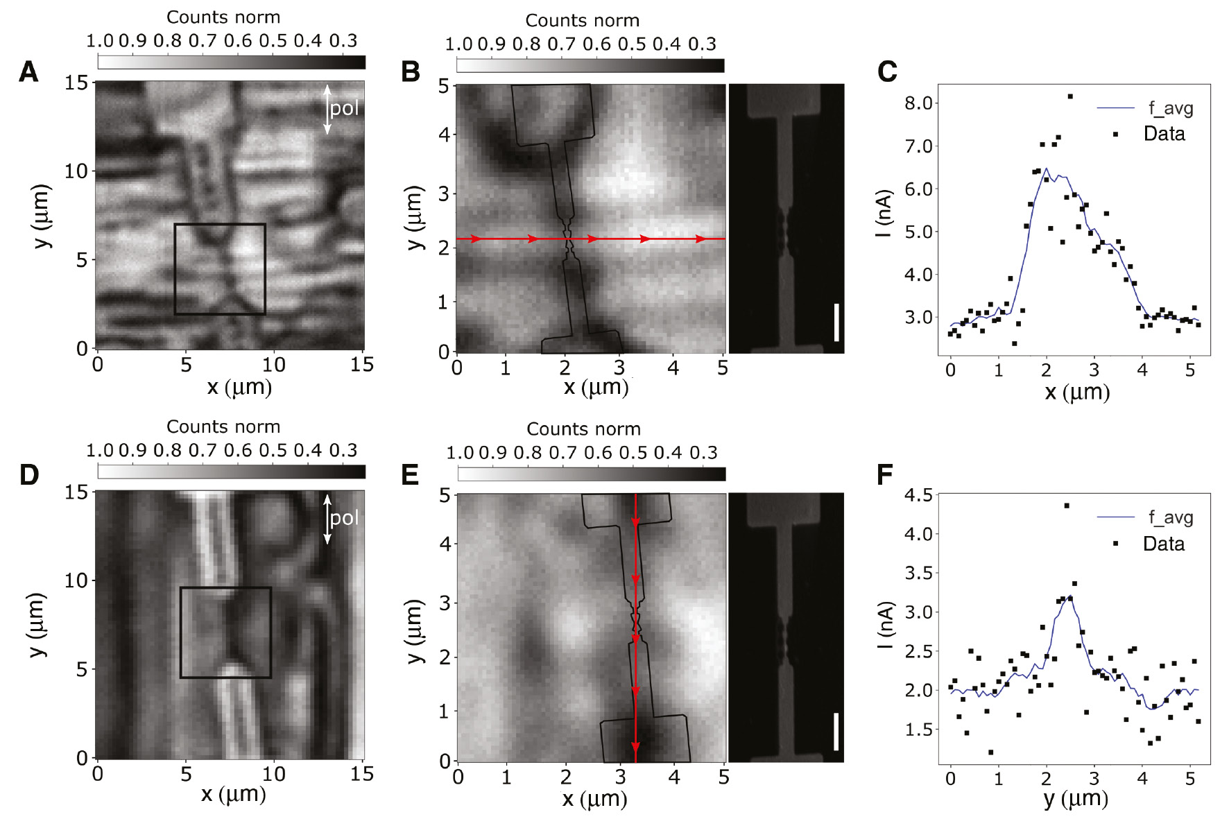
Results of combined optical and electrical measurements.
(A) Scattering image of a break junction with vertical scan direction. The black frame indicates the scan area of (B). (B) Higher-magnification image of the junction area of the break junction shown in (A). The outline of the break junction is overlaid to illustrate the position of the MCBJ. An SEM image of the break junction is displayed next to the image. The scale bar is 1 μm. (C) Current during a horizontal line section. The scan position is depicted in (B) as a red line. (D) Scattering image of a break junction with horizontal scan direction. The black frame indicates the scanning area of (E). (E) Higher magnification image of the junction area of the break junction shown in (D). The measurement is slightly out of focus, resulting in a blurred picture. The outline of the break junction is overlaid to illustrate the position of the MCBJ. An SEM image of the break junction is displayed next to the image. The scale bar is 1 μm. (F) Current during a vertical line section. The scan position is depicted in (E) as a red line.
A scan of the junction area is performed. In Figure 7A, B, D, and E, the scattered intensity from the sample is displayed. In Figure 7A, the image area is scanned vertically column by column from left to right. Figure 7B is a higher-magnification image of the junction area of the MCBJ shown in Figure 7A. To illustrate the position of the MCBJ, the outline of the structure extracted from the SEM image displayed on the right is overlaid. In Figure 7C, the current measured during a horizontal line section through the BT is displayed. The position of the analyzed line is depicted in Figure 7B as a red line. Without illumination, the current is 3 nA. As the laser spot approaches the junction, the current rises significantly and peaks at 8.2 nA. To account for the noise, a floating average is calculated and displayed in the plot. The maximum of the floating average is 6.5 nA. When the laser spot has passed the junction, the current decreases to 3 nA. The scanning direction is rotated by 90° to horizontal scanning for Figure 7D–F. In Figure 7F, the current is displayed for a vertical line section over the junction. The position of the line section is shown in Figure 7E as a red line. Without illumination, the current has stabilized around 2 nA. When the laser spot is in the proximity of the junction area, the current increases to a maximum value of 4.4 nA. The floating average peaks at 3.2 nA. A number of effects may contribute to the increased current shown in Figure 7, such as thermal expansion, photon-assisted tunneling [33], or plasmon-assisted tunneling. Thermal expansion is ruled out by Guhr et al. [13] and Ward et al. [34] for the use of CW lasers.
The additional current through photon-assisted tunneling reported by Ward et al. [34], when corrected for the respective gap widths, appears to have been smaller than the increase observed here. This may be an indication that LSPPs further increase the tunneling probability. In order to better understand the relative contributions of these possible effects, additional experiments need to be carried out. A Yagi-Uda antenna design could be used with the BT at the emitter position. The directors can then be excited, which translates into an excitement of the BT without direct illumination. In any case, the experiment proves the potential of the measurement configuration for simultaneous correlative imaging of the optical scattering and electronic transport information obtained from the MCBJ.
2.6 Optical measurements with 785-nm irradiation
In order to decrease the luminescence background of the PI substrate, a different laser wavelength is used. Choosing a single mode laser with a wavelength of 785 nm, the fluorescence of PI is reduced to less than 1% of the fluorescence at 488-nm excitation. The scattering and luminescence signal of the gold and the nanostructure are now stronger than the background. A break junction with leads at an angle of 45° as in Figure 1D is shown in Figure 8A. The nanostructure in the center of the MCBJ is visible as a bright spot between the leads. The sample is bent in order to break the junction. To verify the scattering image, the SEM image of the same MCBJ is displayed in Figure 8B, and an overlay of Figure 8A and B is shown in Figure 8C. The difference in scattering intensity of the opposite edges of the leads is due to inhomogeneous illumination resulting from the curvature of the bent substrate. Using the 785-nm laser therefore shows the way toward further low-background correlative measurements and to the selective evaluation of the BT’s plasmonic resonance spectrum.

Confocal and SEM images of an MCBJ with oblique leads.
(A) Smoothed scattering image of a bent MCBJ (logarithmic color scale). The image is taken with the confocal microscope using a 785-nm laser for illumination. The arrow indicates the increased scattering at the location of the BT. (B) SEM image of the MCBJ with oblique leads (see also Figure 1D). (C) Scattering image from (A), partly overlaid with the SEM image from (B). The left edges of the leads scatter more strongly than the others. This is due to the bending of the substrate and therefore inhomogeneous illumination.
3 Conclusion
In this work, a flexible platform with corresponding samples for the correlative optical and electrical investigation of ultranarrow gap junctions was developed. The fabrication of well-defined BT nanostructures at the designated breaking point of MCBJs was demonstrated. Two geometries were introduced to partly decouple the nanoantenna from the leads.
A bending device with height-adjustable counter-supports that is compatible with a confocal microscope was designed. The curvature of the sample can be changed by moving the counter-support, while the sample surface at the center pusher stays in the focus of the microscope. The pusher and counter-support were motorized. For measurements at nanogap widths that were not intrinsically stable, a feedback loop was implemented in order to automatically fix the sample at a specific current value. In the tunnel regime, the loop manages to stabilize the current at the target value for around 20 s. The mechanical functionality was proven by electrical measurements, in which quantized conductance was observed, and SEM imaging of bent samples exhibiting a nanoscale gap. The strong luminescence of the substrate turned out to be detrimental for spectroscopic measurements, but experiments with a near-infrared laser source show that increasing the wavelength is a viable strategy to overcome these difficulties. Nevertheless, the correlative measurements of the tunneling current and scattered light showed an increased tunneling current whenever the junction area was illuminated. The enhancement of the tunneling current measured in the present work showed higher values than reported in the existing literature on photon-assisted tunneling at subnanometer gaps. This may indicate that an excitation of LSPPs in the dimer nanostructures at the junction could further boost the tunneling efficiency. The novel bending setup for simultaneous optical and transport measurements together with the tailored plasmonic MCBJ samples opens the way for many further experiments on light-induced charge processes in ultranarrow gaps or at ultrashort channel lengths.
4 Materials and methods
4.1 Fabrication
For the sample preparation, a 350-μm-thick sheet of steel is cut into 1×7-cm2 pieces. Polyimide (PI 2610; DuPont, Wilmington, DE, USA) is spin-coated on top of the steel substrates forming a flat 3- to 5-μm-thin layer on the rather rough surface. The PI is cured in an oven under nitrogen atmosphere. The temperature is increased from room temperature to 350°C with a ramp of 4°C/min. When the maximum is reached, the temperature is held for 30 min and then passively lowered to room temperature by switching off the heaters. After the curing process, a 130-nm-thick polymethyl methacrylate (PMMA) layer is spin-coated onto the PI. The PMMA is structured via electron beam lithography performed with a FEI XL-30 SEM and a XENOS XPA 2 pattern generator. The beam energy is 30 keV. In the center of the exposed pattern, a connected BT nanostructure is located. The BT consists of two equally sized triangles pointing toward each other. The triangle dimensions are in the range of 100 to 200 nm. For plasmonic break junctions, the triangles touch each other forming a 10- to 20-nm bridge. This connection is the thinnest part of the whole pattern, acting as the designated breaking point of the MCBJ. Each triangle of the BT is separately connected by leads, which emerge from the back of the triangles. The leads are getting stepwise wider with increasing distance to the BT. The electron beam exposure pattern is shown in Figure 1A (orange), and e-beam defined structures are shown in Figure 1C and D.
After the exposure, the resist is developed for 70 s in a 1:3 mixture of methylisobutylketone and isopropyl alcohol at room temperature. After the development, the sample is metalized with a 30-nm-thick gold layer via thermal evaporation. For the following lift-off, the sample is immersed in an acetone bath. Now a UV-sensitive resist (maP-1215, microchemical resist) is spin-coated onto the substrate. A mask with the macroscopic leads is aligned with respect to the e-beam structure. On the one hand, leads connecting the e-beam-defined lines to the voltage source are patterned. In addition, a macroscopic line is integrated into the UV mask, which is shortcutting the break junction via the leads by forming a U-shape to protect it from externally induced charging and currents that might destroy the junction during the following fabrication steps and transportation. After the 35-s UV exposure and 35-s development in maD 331 (microresist technology) at room temperature, a second thermal metallization is performed. The UV structure is shown in Figure 1A (red) and Figure 1B. One hundred nanometer of gold is evaporated onto the sample, and the lift-off is performed again in an acetone bath. Before the measurement, the macroscopic shortcut is manually lifted by scratching through the gold line.
To promote the breaking of the MCBJ under strain, the lithographically determined breaking point must be underetched. This is done via RIE of the PI. The gases used are 80% oxygen (O2) and 20% carbon tetrafluoride (CF4). The process pressure is 100 mTorr, and the microwave power is 50 W. The vertical etch rate for PI with these parameters is determined to 100 nm/min and the horizontal etch rate to 50 nm/min. The etch time is originally determined by SEM imaging of the e-beam structures. The goal is to underetch the designated breaking point, but still provide sufficient support of the nanostructured junction area (Figure 1C). The fabrication process is schematically depicted in Figure 9. After the sample is mounted into the measuring setup, both sides of the MCBJ are connected to wires. Both wires are at the same potential. The shortcutting line is interrupted by mechanical scratching. Right before the experiment, the two wires are connected to a DC voltage source and ammeter.

Schematic illustration of the fabrication process.
(A) Metallic substrate with PI layer, (B) spin coating of a PMMA layer as e-beam resist, (C) E-beam exposure, (D) development, (E) thermal evaporation of a gold layer, (F) lift-off, (G) spin coating of maP 1215 UV resist, (H) UV lithography, (I) development, (J) thermal evaporation of a gold layer, (K) lift-off, (L) RIE.
4.2 Characterization
During the bending process, a bias voltage of 50 mV is applied to the MCBJ, and the current is continuously monitored. The sample is prebent with the central pushing rod (motor 1) until the current drops by an order of magnitude. Now the objective is moved upward until the designated breaking point of the break junction is in focus. The sample is then further bent with the outer pusher (motor 2) until the conductance is well below G0 and the tunneling regime is reached. For the first measurements, all screws are manually operated. When a constant tunneling current is reached, a simultaneous optical and electrical measurement is carried out. A CW laser of either 488- or 785-nm wavelength is employed for excitation. Therefore, a 15×15 or 5×5 μm2 square around the designated breaking point is measured with 64×64 pixels by scanning the sample (P-517.3CL; Physik Instrumente, Karlsruhe, Germany) through the laser focus of the confocal microscope, resulting in a pixel spacing of 234 or 78 nm, respectively, whereas the focus size of the linearly polarized Gaussian beam is ~300 nm (500 nm) in diameter for 488-nm (785-nm) excitation. Depending on the filter set used, either the scattered light or the luminescence of the sample can be investigated. For each pixel, the scattered intensity is measured via an avalanche photodiode (APD) with a 5-ms exposure time. Alternatively to the APD, a grating spectrometer (Acton SpectraPro 2300, Princeton Instruments, Trenton, NJ, USA) equipped with a cooled CCD camera (iDus 401, Oxford Instruments, Abingdon, UK) can be used to record the light from the sample. The measured electrical current is averaged for each pixel over the exposure time used for the optical measurement.
Acknowledgments
Financial support by Deutsche Forschungsgemeinschaft through the DFG Grants FL670/7-1 and BR532/1-1, Funder Id: http://dx.doi.org/10.13039/501100001659 and the Open Access Publishing Fund of University of Tübingen is gratefully acknowledged.
References
[1] Wang L, Wang L, Zhang L, Xiang D. Advance of mechanically controllable break junction for molecular electronics. Top Curr Chem 2017;375:61.10.1007/978-3-030-03305-7_2Suche in Google Scholar
[2] Krans JM, Muller CJ, Yanson IK, Govaert TCM, Hesper R, van Ruitenbeek JM. One-atom point contacts. Phys Rev B 1993;48:14721–4.10.1103/PhysRevB.48.14721Suche in Google Scholar
[3] Moreland J, Ekin JW. Electron tunneling experiments using Nb-Sn “break” junctions. J Appl Phys 1985;58:3888.10.1063/1.335608Suche in Google Scholar
[4] van Ruitenbeek JM, Alvarez A, Pineyro I, et al. Adjustable nanofabricated atomic size contacts. Rev Sci Instrum 1996;67:108.10.1063/1.1146558Suche in Google Scholar
[5] Hoffmann R, Weissenberger D, Hawecker J, Stoffler D. Conductance of gold nanojunctions thinned by electromigration. Appl Phys Lett 2008;93:043118.10.1063/1.2965121Suche in Google Scholar
[6] Zhou C, Muller CJ, Deshpande MR, Sleight JW, Reed MA. Microfabrication of a mechanically controllable break junction in silicon. Appl Phys Lett 1995;67:1160–2.10.1063/1.114994Suche in Google Scholar
[7] Makk P, Tomaszewski D, Martinek J, et al. Correlation analysis of atomic and single-molecule junction conductance. ACS Nano 2012;6:3411–23.10.1021/nn300440fSuche in Google Scholar PubMed
[8] van Wees BJ, van Houten H, Beenakker CWJ, et al. Quantized conductance of point contacts in a two-dimensional electron-gas. Phys Rev B 1988;60:848–50.10.1103/PhysRevLett.60.848Suche in Google Scholar PubMed
[9] Wharam DA, Thornton TJ, Newbury R, et al. One-dimensional transport and the quantization of the ballistic resistance. J Phys C Solid State 1988;21:L209–14.10.1088/0022-3719/21/8/002Suche in Google Scholar
[10] Simmons JG. Generalized formula for the electric tunnel effect between similar electrodes separated by a thin insulating film. J Appl Phys 1963;34:1793–1803.10.1063/1.1702682Suche in Google Scholar
[11] Binnig G, Rohrer H. Scanning tunneling microscopy. Helv Phys Acta 1982;55:726–35.10.1007/978-1-4615-7682-2_1Suche in Google Scholar
[12] Konishi T, Kiguchi M, Takase M, et al. Single molecule dynamics at a mechanically controllable break junction in solution at room temperature. J Chem Soc 2013;135:1009–14.10.1021/ja307821uSuche in Google Scholar PubMed
[13] Guhr DC, Rettinger D, Boneberg J, Erbe A, Leiderer P, Scheer E. Influence of laser light on electronic transport through atomic-size contacts. Phys Rev Lett 2007;99:086801.10.1103/PhysRevLett.99.086801Suche in Google Scholar PubMed
[14] Guhr DC, Rettinger D, Boneberg J, Erbe A, Leiderer P, ScheerE.Influence of chopped laser light onto the electronic transport through atomic-sized contacts. J Microsc 2008;229:407–14.10.1111/j.1365-2818.2008.01920.xSuche in Google Scholar PubMed
[15] Benner D, Boneberg J, Nurnberger P, Ghafoori G, Leiderer P, Scheer E. Transmission of surface plasmon polaritons through atomic-size constrictions. New J Phys 2013;15:113014.10.1088/1367-2630/15/11/113014Suche in Google Scholar
[16] Ghafoori G, Boneberg J, Leiderer P, Scheer E. Tuning the transmission of surface plasmon polaritons across nano and micro gaps in gold stripes. Opt Express 2016;24:17313–20.10.1364/OE.24.017313Suche in Google Scholar PubMed
[17] Giannini V, Fernández-Domínguez AI, Heck SC, Maier SA. Plasmonic nanoantennas: fundamentals and their use in controlling the radiative properties of nanoemitters. Chem Rev 2011;111:3888–912.10.1021/cr1002672Suche in Google Scholar PubMed
[18] Petryayeva E, Krull UJ. Localized surface plasmon resonance: Nanostructures, bioassays and biosensing—a review. Anal Chim Acta 2011;706:8–24.10.1016/j.aca.2011.08.020Suche in Google Scholar PubMed
[19] Nordlander P, Oubre C, Prodan E, Li K, Stockman MI. Plasmon hybridization in nanoparticle dimers. Nano Lett 2004;4:899–903.10.1021/nl049681cSuche in Google Scholar
[20] Jain PK, Huang W, El-Sayed MA. On the universal scaling behavior of the distance decay of plasmon coupling in metal nanoparticle pairs: a plasmon ruler equation. Nano Lett 2007;7:2080–8.10.1021/nl071008aSuche in Google Scholar
[21] Laible F, Gollmer DA, Dickreuter S, Kern DP, Fleischer M. Continuous reversible tuning of the gap size and plasmonic coupling of bow tie nanoantennas on flexible substrates. Nanoscale 2018;10:14915.10.1039/C8NR03575JSuche in Google Scholar
[22] Fromm DP, Sundaramurthy A, Schuck PJ, Kino G, Moerner WE. Gap-dependent optical coupling of single “bowtie” nanoantennas resonant in the visible. Nano Lett 2004;4:957–61.10.1021/nl049951rSuche in Google Scholar
[23] Zuloaga J, Prodan E, Nordlander P. Quantum description of the plasmon resonances of a nanoparticle dimer. Nano Lett 2009;9:887–91.10.1021/nl803811gSuche in Google Scholar PubMed
[24] Bai J, Daaoub A, Sangtarash S, et al. Anti-resonance features of destructive quantum interference in single-molecule thiophene junctions achieved by electrochemical gating. Nat Mater 2019;18:364–9.10.1038/s41563-018-0265-4Suche in Google Scholar PubMed
[25] Kergueris C, Bourgoin JP, Palacin S, et al. Electron transport through a metal-molecule–metal junction. Phys Rev B 1999;59:12505–13.10.1103/PhysRevB.59.12505Suche in Google Scholar
[26] Reed MA, Zhou C, Muller CJ, Burgin TP, Tour JM. Conductance of a molecular junction. Science 1997;278:252–4.10.1126/science.278.5336.252Suche in Google Scholar
[27] Taniguchi M, Tsutsui M, Yokota K, Kawai T. Inelastic electron tunneling spectroscopy of single-molecule junctions using a mechanically controllable break junction. Nanotechnology 2009;20:434008.10.1088/0957-4484/20/43/434008Suche in Google Scholar PubMed
[28] Aiba A, Iwane M, Fujii S, Kiguchi M. Electronic properties of single atom and molecule junctions. ChemElectroChem 2018;5:2508–17.10.1002/celc.201800787Suche in Google Scholar
[29] Costa-Krämer JL, García N, Olin H. Conductance quantization histograms of gold nanowires at 4 K. Phys Rev B 1997;55:12910–3.10.1103/PhysRevB.55.12910Suche in Google Scholar
[30] Kiguchi M, Sekiguchi N, Murakoshi K. Electric conductance of metal nanowires at mechanically controllable break junctions under electrochemical potential control. Surf Sci 2007;601:5262–5265.10.1016/j.susc.2007.04.218Suche in Google Scholar
[31] Wang QL, Liu R, Xiang D, et al. Single-atom switches and single-atom gaps using stretched metal nanowires. ACS Nano 2016;10:9695–702.10.1021/acsnano.6b05676Suche in Google Scholar PubMed
[32] Yang Y, Liu JY, Feng S, et al. Unexpected current-voltage characteristics of mechanically modulated atomic contacts with the presence of molecular junctions in an electrochemically assisted-MCBJ. Nano Res 2016;9:560–70.10.1007/s12274-015-0937-1Suche in Google Scholar
[33] Stolz A, Berthelot J, Mennemanteuil MM, et al. Nonlinear photon-assisted tunneling transport in optical gap antennas. Nano Lett 2014;14:2330–8.10.1021/nl404707tSuche in Google Scholar PubMed
[34] Ward DR, Huser F, Pauly F, Cuevas JC, Natelson D. Optical rectification and field enhancement in a plasmonic nanogap. Nat Nanotechnol 2010;5:732–6.10.1038/nnano.2010.176Suche in Google Scholar PubMed
©2020 Florian Laible, Kai Braun, Monika Fleischer et al., published by De Gruyter, Berlin/Boston
This work is licensed under the Creative Commons Attribution 4.0 International License.
Artikel in diesem Heft
- Reviews
- Multiparticle quantum plasmonics
- Physics and applications of quantum dot lasers for silicon photonics
- Integrated lithium niobate photonics
- Subwavelength structured silicon waveguides and photonic devices
- Nonlinear optical microscopies (NOMs) and plasmon-enhanced NOMs for biology and 2D materials
- Enhancement of upconversion luminescence using photonic nanostructures
- 3D Nanophotonic device fabrication using discrete components
- Research Articles
- A flexible platform for controlled optical and electrical effects in tailored plasmonic break junctions
- Effects of roughness and resonant-mode engineering in all-dielectric metasurfaces
- Colloidal quantum dots decorated micro-ring resonators for efficient integrated waveguides excitation
- Engineered telecom emission and controlled positioning of Er3+ enabled by SiC nanophotonic structures
- Diffraction engineering for silicon waveguide grating antenna by harnessing bound state in the continuum
- On-chip scalable mode-selective converter based on asymmetrical micro-racetrack resonators
- High-Q dark hyperbolic phonon-polaritons in hexagonal boron nitride nanostructures
- Multilevel phase supercritical lens fabricated by synergistic optical lithography
- Continuously-tunable Cherenkov-radiation-based detectors via plasmon index control
- Cherenkov radiation generated in hexagonal boron nitride using extremely low-energy electrons
- Geometric phase for multidimensional manipulation of photonics spin Hall effect and helicity-dependent imaging
- Stable blue-emissive aluminum acetylacetonate nanocrystals with high quantum yield of over 80% and embedded in polymer matrix for remote UV-pumped white light–emitting diodes
- Pumping-controlled multicolor modulation of upconversion emission for dual-mode dynamic anti-counterfeiting
- Broadband graphene-on-silicon modulator with orthogonal hybrid plasmonic waveguides
- Non-noble metal based broadband photothermal absorbers for cost effective interfacial solar thermal conversion
- Metal-insulator-metal nanoresonators – strongly confined modes for high surface sensitivity
- Erratum
- Erratum to: Darkfield colors from multi-periodic arrays of gap plasmon resonators