All-in-one silicon photonic polarization processor
-
Hailong Zhou
 ,
Yuhe Zhao
,
Yuhe Zhao
 and
Xinliang Zhang
and
Xinliang Zhang

Abstract
With the great developments in optical communication technology and large-scale optical integration technology, it is imperative to realize the traditional functions of polarization processing on an integration platform. Most of the existing polarization devices, such as polarization multiplexers/demultiplexers, polarization controllers, polarization analyzers, etc., perform only a single function. Definitely, integrating all these polarization functions on a chip will increase function flexibility and integration density and also cut the cost. In this article, we demonstrate an all-in-one chip-scale polarization processor based on a linear optical network. The polarization functions can be configured by tuning the array of phase shifters on the chip. We demonstrate multiple polarization processing functions, including those of a multiple-input-multiple-output polarization descrambler, polarization controller, and polarization analyzer, which are the basic building blocks of polarization processing. More functions can be realized by using an additional two-dimensional output grating. A numerical gradient descent algorithm is employed to self-configure and self-optimize these functions. Our demonstration suggests great potential for chip-scale, reconfigurable, and fully programmable photonic polarization processors with the artificial intelligence algorithm.
1 Introduction
Polarization, as one of the fundamental physical characteristics of light, has a great impact on many fields of photonics, including optical communication [1], [2], [3], optical imaging [4], and quantum optics [5]. Manipulation of the state of polarization (SOP) of light is fundamental for these applications. With the rapid development of large-scale optical integration technology, numerous on-chip polarization processing devices have been proposed, such as the polarization beam splitter (PBS) [6], [7], [8], [9], polarization splitter-rotator (PSR) [10], polarization rotator (PR) [11], [12], polarization controller [13], [14], [15], [16], and polarization analyzer [17], [18], [19], [20], [21], since an integrated photonic polarization device usually has a much smaller footprint and higher power efficiency. These functions are the basic building blocks for polarization signal processing and show important applications. For example, the PSR, PBS, and PR can be combined to multiplex and demultiplex two orthogonally polarized beams, acting as a polarization multiplexer/demultiplexer [2], [22], [23]. Moreover, a multiple-input-multiple-output (MIMO) algorithm is further needed to descramble the two channels when the SOPs are changed or even become non-orthogonal, caused by crosstalk and unbalanced loss [24]. Unfortunately, the MIMO algorithms suffer from heavy computation requirements for high-bandwidth electronic hardware. Alternatively, all-optical MIMO descramblers were developed to descramble the modes with the inherent speed of light [25], [26], [27]; however, all-optical MIMO descramblers are rarely reported in the realm of polarization. A polarization controller is an optical device that allows arbitrary modification of the SOP of light. Polarization controllers can be implemented with free-space optics, through a fiber pigtailed U-bench, or with integrated optical devices [13], [14], [15], [16], [28]. An integrated polarization controller is usually composed of PRs and phase shifters. Integrated polarization controllers based on different materials such as polymer [16] and silicon [13], [14], [15] have been developed. The SOP of light can be measured by a polarization analyzer. Typically, the issue of SOP measurement has been addressed by dividing the signal spatially or temporally [4]. Division-of-space polarization analyzers divide the input beam into multiple optical paths, with each path aiming to get different polarization information. Some integrated schemes based on plasmonic nanostructures and metasurfaces have been reported [29], [30], [31]. Also, silicon-based schemes have been suggested [18], [19], [21]. For division-of-time methods, different polarization information is measured at different times [32], [33]. For example, two Mach-Zehnder interferometers (MZIs) with a two-dimensional (2D) grating could be combined to form an integrated division-of-time polarization analyzer based on the polarization-frequency mapping technique [17]. In view of both the advantages of silicon-on-isolator (SOI) devices and the necessity of on-chip polarization management, SOI-based polarization analyzers and polarization controllers are highly desirable. Although various integrated functional devices for polarization processing have been developed, most of them show limited reconfigurability, resulting in poor robustness and high cost. An effective solution is to implement multipurpose polarization processing in an optical network with a reconfigurable and integrated polarization processor.
In recent years, some programmable optical devices have been developed. For example, a universal linear optical network was rapidly reprogrammed to implement various quantum applications [34]. Other devices for radio frequency applications [35] and photonics signal processing [36], [37], [38], [39] have also been reported. These programmable optical processors show great advantages in reconfigurability and self-configuration capability. They are reconfigurable for multiple functions, self-configurable with some learning ability, and field-programmable with strong fabrication tolerance. Inspired by programmable optics, it is possible to implement a reconfigurable and programmable polarization processor with a linear optical network.
In this article, we propose an all-in-one chip-scale polarization processor based on a linear optical network. The chip contains a 2D grating and four MZIs, which can complete an arbitrary linear transformation by thermal tuning of the phase shifters. By tuning the transmission matrix of the network, the chip can be configured as a polarization MIMO descrambler, a polarization controller, and two kinds of polarization analyzers. A numerical gradient descent algorithm is employed to self-configure and self-optimize these functions. Our demonstration suggests great potential for chip-scale reconfigurable and fully programmable photonic polarization processing with the artificial intelligence (AI) algorithm.
2 Principle
The photonic polarization processor is composed of a 2D grating and four MZIs, as shown in Figure 1A. The 2D grating splits the two orthogonal components (defined as x and y polarizations) of the input light into different waveguide branches with the same TE mode. Both MZI 1 and MZI 4 can perform any arbitrary 2×2 unitary matrix transformation [40], [41], [42], [43], [44], [45]. The combination of MZIs 2 and 3 can perform an arbitrary 2×2 diagonal matrix transformation. The four MZIs constitute a complete network that can implement an arbitrary transformation matrix based on singular value decomposition [45], [46]. The light is coupled to the fiber array from the chip with TE gratings. By designing the transmission matrix, the chip is reconfigured to achieve three different functions.
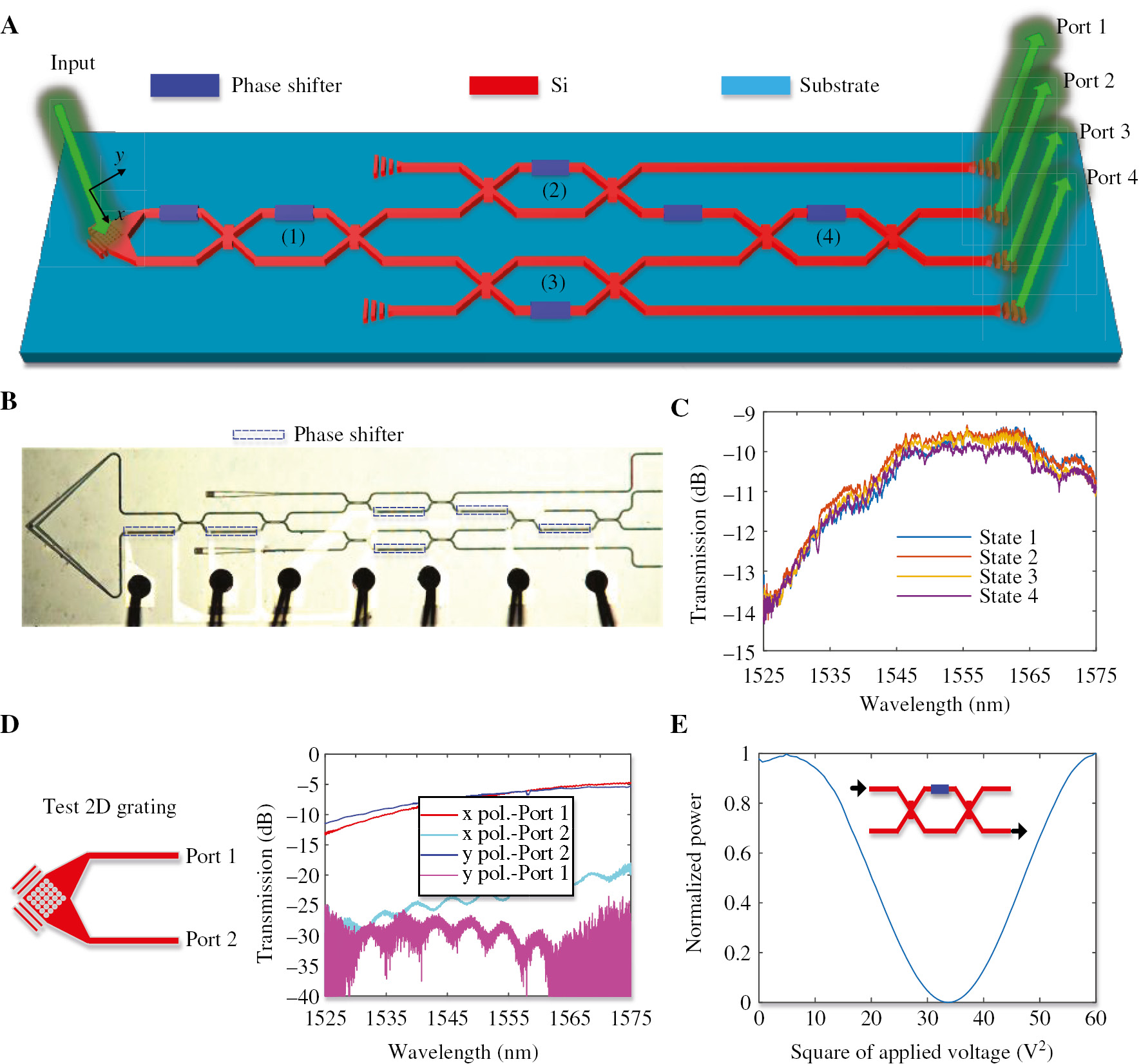
Photonic polarization processing circuits.
(A) Detailed structure of the polarization processor chip. (B) Micrograph of fabricated chip. (C) Transmission spectra of the chip for random input SOPs and applied voltages. (D) Transmission spectra of the 2D grating. (E) Imparted phase depending on the applied voltage for the tested MZI structure.
Usually, the SOPs of two polarization channels are orthogonal and set as x and y polarizations. While crosstalk between different channels will be introduced both in the optical transmission link and in the mode multiplexer/demultiplexer, the SOPs of two channels will be changed or even become non-orthogonal. Assume that the Jones matrices of two channels in the receiving end are P and Q, respectively, given by
In order to separate the two channels, a transformation matrix is needed to meet
Here, ᴧ=[A1, A2] is a diagonal matrix, representing the optical field distribution in the output ports (Ports 2 and 3) for two channels. The transformation matrix is then given by
From the above analysis, the P-polarized component (Channel 1) of the input light will emerge from Port 2 and the Q-polarized one (Channel 2) will emerge from Port 3. Similarly, the output ports can be switched by rotating the diagonal matrix by 90°. It proves that our chip is able to separate two arbitrary polarization-based channels in theory, which can be used to descramble the polarization-based channels.
Meanwhile, our chip can also transform an arbitrary polarization into a fixed known one and transform a fixed known polarization into an arbitrary one in reverse, acting as a polarization controller. The transformation matrix is given by
Here, P⊥ is the cross-polarization of P. When P-polarized light is incident on the 2D grating, only one output port will excite the light. And in the reverse, arbitrarily polarized light can be generated and emerge from the 2D grating when the light is incident on one of the output ports.
Furthermore, the four ports can output different polarization information, which can be used to measure the SOP of light, making the chip as a division-of-space polarization analyzer. The Stokes parameters S=[S0, S1, S2, S3] can be obtained by [30]
where I=[I1, I2, I3, I4] is the measured optical power in the four output ports. T is a 4×4 matrix dependent on the internal parameters of chip. The four intensities of the different polarized components can be equivalently obtained at different times by applying four sets of direct current (DC) voltage signals on the phase shifters, making the chip as a division-of-time polarization analyzer.
The key point to configure these polarization functions is how to load a targeted transformation matrix on the chip. Here we employ a numerical gradient descent algorithm modified from deep learning [46], [47] to optimize this issue. According to the different purposes of our processor, a suitable and special cost function (CF) should be first defined. Then the only training target is to make the defined CF maximum using the numerical gradient descent algorithm. Theoretically, training needs to combine forward and backward propagation methods, similar to deep learning. Forward propagation is used to calculate the output as the data for the next iteration, and then backward propagation aims to estimate the errors and find the gradient descent. This training algorithm is also called the gradient descent algorithm, which is a common method for training artificial neural networks (ANNs). In our design, the optical chip can output automatically and timely provided the input is set. And the gradient descent can be alternatively measured by fine-tuning each parameter. So in our design, no backward propagation is needed and forward propagation can be implemented by the chip itself at the speed of light. Furthermore, the chip can be regarded as a “black box”. That means the internal structure of the chip is transparent to the users. The full training process is as follows:
Initialization: all the adjustable parameters θ(i=1, 2, …) are set randomly. Here, θi is the carried phase on the corresponding phase shifter.
Tuning each parameter: set θ1 to θ1+Δθ temporarily.
If CF(θ1+Δθ)≥CF(θ1), replace θ1 with θ1+Δθ; else, replace θ1 with θ1−Δθ.
Repeat Step 2 for all adjustable parameters one by one.
Repeat Steps 2 and 3 until the CF is converged or reach the target value.
For the polarization MIMO descrambler, the CF is defined independently of the channel by
The operation “•” means the scalar product of two vectors. Aexpn (n=1, 2) is the measured output power distribution in Ports 2 and 3 when only Channel n is open.
Similarly, the CF of the polarization controller is defined by
Here, Pow is the desired output power distribution in four ports and Powexp is the measured one. For example, Pow can be set as [0, 1, 0, 0] if we want to make all the light output from Port 2.
CF ranges from 0 to 1, where CF=0 means that the experimental results are completely inconsistent with the targeted results and CF=1 means that they are completely consistent. Our training target is to make CF as close to 1 as possible. To guarantee power efficiency, the first eigenvalue of the transmission matrix is fixed to 1; namely the phase difference of two inner arms of the second MZI in Figure 1A is always equal to π and there is no light output from Port 1. In the following, the chip is reconfigured to achieve three different functions.
3 Results
3.1 Experimental setup
The chip is fabricated on a commercial silicon-on-insulator (SOI) wafer. A passive process is employed to fabricate the structure on the SOI wafer with a 220-nm top silicon layer, a 2-μm silica cladding layer, and a 2-μm-thick buried oxide (BOX) substrate. The size of chip is about 2.0 mm×0.5 mm. The micrograph of the fabricated chip is shown in Figure 1B. The transmission spectra of the chip are shown in Figure 1C, which are measured by summing the output power of four ports when the input SOP and the applied voltages are both random. The transmission at 1550 nm is about –10 dB (excluding the output TE gratings), and the 3-dB bandwidth is about 40 nm (1535–1575 nm). The 2D grating coupler consists 17 rows and columns of holes of diameter 360 nm and shallow etch of 70 nm. The holes are arranged in the circular lattice with the average period of 635 nm. The transmission spectra of the 2D grating are shown in Figure 1D. The insertion loss at 1550 nm for two polarizations is about 6.5 dB, and the polarization extinction ratios are larger than 15 dB for both polarizations in the entire C-band. The imparted phase, which depends on the applied voltage (V), may be expressed as θ=2πV2/T [46]. MZIs with internal phase shifters are used to convert the phase change into output power. The measured power distribution, which depends on the square of the applied voltage, is presented in Figure 1E. The measured average period of T is about 55V2. The phase tuning efficiency is measured to be 27 mW per π phase shift, and the electrical resistance is about 1000 Ω. The response speed of thermo-optic phase shifters is larger than 10 kHz [17]. The network training (typically <1000 iterations) can be completed within 100 ms provided the external driver is fast enough. Figure 2 presents the experimental setup. The setup for polarization multiplexing is depicted in Figure 2A. The two channels (SOP1 and SOP2) are independently configured with lasers, single-mode fibers (SMFs), and polarization controllers (PCs). Then they are combined with an optical coupler (OC). Two optical switches (OSs) powered by electricity are inserted in the paths to open or close the corresponding channel. Figure 2B presents the setup for polarization preparation. Any arbitrary or known SOP can be generated by rotating the wave plates (WPs), which contain a half-WP and a quarter-WP. The combined light in Figure 2A or the generated polarized light in Figure 2B is injected to the chip with a 2D grating for subsequent processing. Figure 2C presents the setup for polarization processing. A V-groove fiber array (VGA) and a four-channel photodetector array (PDA) are used to receive the output light from the chip. All the phase shifters in the chip and the OSs are driven by a voltage source array (VSA). All the monitoring instruments and voltage sources are connected and controlled by the same computer.
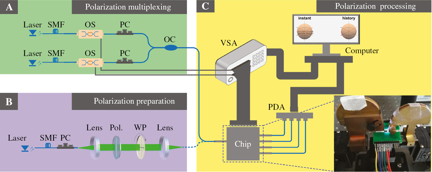
Experimental setup.
(A) Polarization multiplexing: two polarization channels are independently configured and then combined. (B) Polarization preparation: an arbitrary and known SOP can be generated by rotating the wave plates (WPs), which contain a half-WP and a quarter-WP. (C) Polarization processing: all the phase shifters in the chip are driven by a voltage source array (VSA), and the output light is collected by a photodetector array (PDA). The PDA and VSA are connected and controlled by the same computer. The inset shows the details of chip packaging.
3.2 Polarization MIMO descrambler
Crosstalk between different channels always exists both in the optical transmission link and in the polarization multiplexer/demultiplexer. Here, all-optical MIMO demultiplexing can be accomplished with our chip. The experimental devices in Figure 2A,C are used to configure the polarization MIMO descrambler. The SOPs of two channels are randomly set by tuning the PCs in Figure 2A, to emulate the optical transmission link and polarization multiplexing with crosstalk accumulation. The two channels can be separated using the self-configuring method, and the CFs in Eq. (6) are used to optimize the problem. Figure 3A presents the training process as a function of the number of iterations (Video S1). The CF is near 0.63 before the training, indicating the two channels are strongly mixed and the crosstalk is quite large. Then the CF is gradually increased with the training algorithm and finally reaches near 1 (0.9999). Figure 3B presents the light power distributions when the number of iterations equals 1, 10, and 40. One can see that the crosstalk can be eliminated using the optimization algorithm, which finally is below –20 dB at 1550 nm. We tested six random states (Cases 1–6), where the SOPs of two channels are randomly set by tuning the PCs in Figure 2A. The normalized transmission spectra for the two channels are measured and presented in Figure 4A,B for the routing states SOP 1-Port 2 and SOP 2-Port 3. The crosstalk is less than –10 dB in a bandwidth of ~9 nm. The routing state can be also switched, and the measured transmission spectra (routing state: SOP1-Port3, SOP2-Port2) for Case 6 are shown in Figure 4C,D. The crosstalk is less than –20 dB at 1550 nm and less than –10 dB in a bandwidth of ~7 nm. It proves that our chip can function as a polarization MIMO descrambler and a polarization switch.
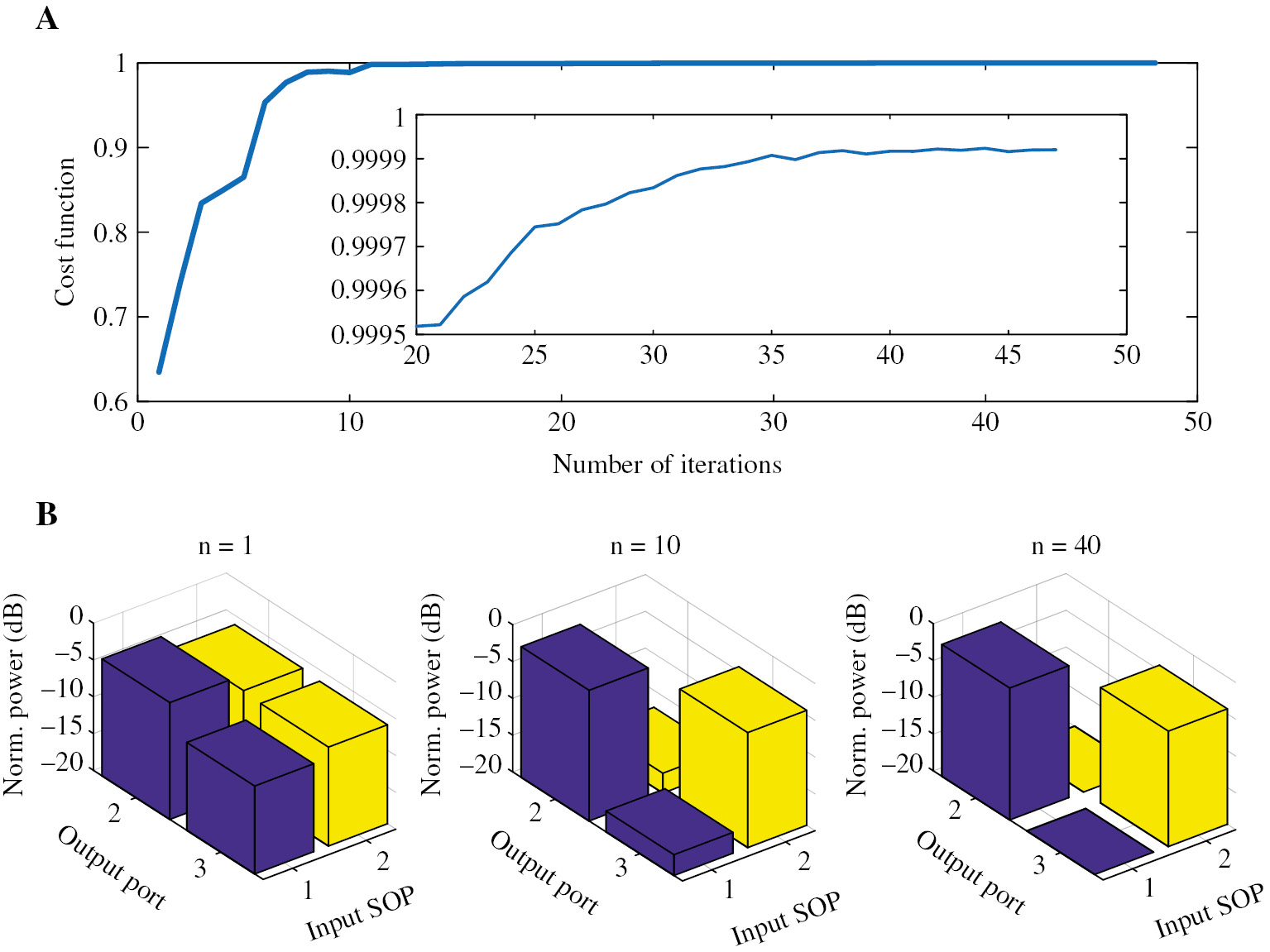
Training process for polarization MIMO descrambler.
(A) Cost function dependent on the number of iterations (Video S1). (B) Light power distributions when the number of iterations equals 1, 10, and 40.
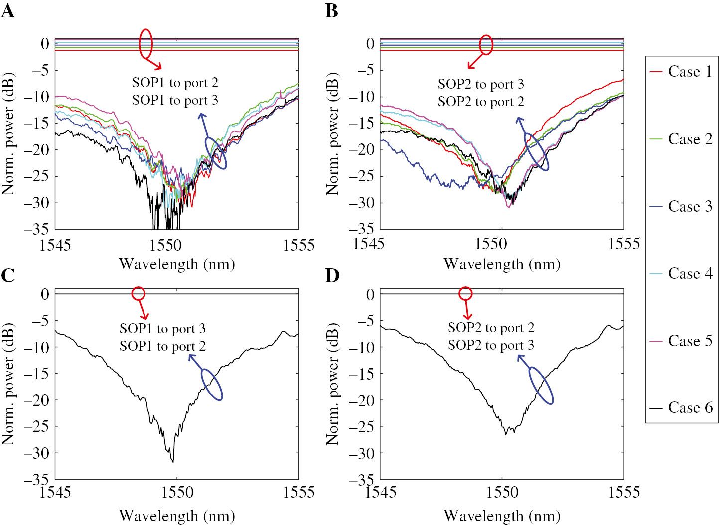
Transmission spectra for polarization MIMO descrambler and polarization switch.
Six random states are tested. (A, B) Routing state: SOP 1–Port 2, SOP 2–Port 3. (C, D) Routing state: SOP 1–Port 3, SOP 2–Port 2.
3.3 Polarization controller
The chip can also be configured as a polarization controller. A polarization controller can transform an arbitrary polarization into a fixed, known one. In our experiment, one of the channels in Figure 2A is used to generate light with random and unknown SOP. And an arbitrary output port can be set as the targeted port to make all the light output from this port. Figure 5A shows an example where Port 4 is the targeted output port (Video S2). The CF in Eq. (7) is used to optimize this kind of problem and train the network. The CF can reach up to 0.999 after 174 rounds of iterations. Figure 5B presents the light power distributions when the number of iterations equals 1, 25, 50 and 174. We can see that the light gradually accumulates at Port 4 and recedes from the other ports correspondingly. Finally, the extinction ratio can be less than –20 dB at 1550 nm. In further experiments, we tested 10 samples of different random SOPs as the initial SOPs. The targeted ports were randomly assigned. The goal was to make light emerge at the assigned port. The measured transmission spectra (including the TE grating couplers) are shown in Figure 5C. The extinction ratio can be less than –18 dB at 1550 nm for all cases.
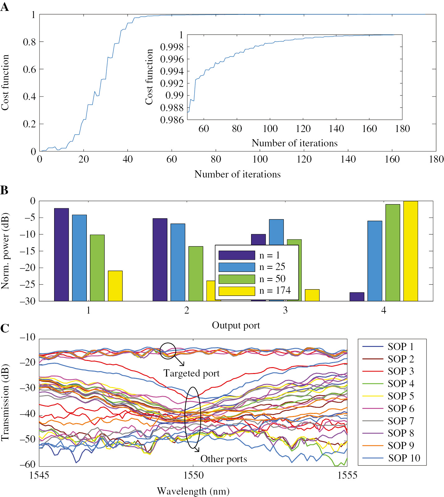
Experimental results for polarization controller.
(A) Cost function dependent on the number of iterations (Video S2). (B) Light power distributions when the number of iterations equals 1, 25, 50, and 174. (C) Transmission spectra (including the TE grating couplers) for 10 cases with random SOPs and random targeted ports.
In the reverse, the polarization controller can transform a fixed, known polarization into an arbitrary one. In this case, we can inject light into the chip from any arbitrary output port, and the light with a specified SOP can emerge from the 2D grating. Both forward and backward trainings can be used to implement polarization control.
3.4 Polarization analyzer
In our chip, the MZIs are asymmetrically designed, thus introducing phase differences in both the internal and external arms. As a result, four output ports can represent different polarization information, acting as a division-of-space polarization analyzer. The systematic structure is shown in Figure 6A. Here, all phase shifters do not work during the experiment. Namely, we do not apply any voltage on the phase shifters. The input SOPs are prepared with the setup in Figure 2B. A half-WP and a quarter-WP are used to generate an arbitrary and known SOP. Then the output power of different polarized components is received by the PDA. First, the transmission matrix T in Eq. (5) is calibrated by using the four known SOPs in advance. The theoretical SOPs can be calculated according to the readings of WPs. Then the chip can be used to measure the Stokes parameters of unknown input light according to Eq. (5). The Stokes parameters are measured and marked on the Poincaré sphere, as shown in Figure 6B. One can see that the experimental results are well consistent with the theoretical results. A live demo is recorded (Video S3), where the half-WP is rotated continuously, whereupon the measured SOPs should rotate by a circle around the center of the sphere. The ellipticity angle of SOP (labeled by χ) and the orientation angle of SOP (labeled by φ) are defined by
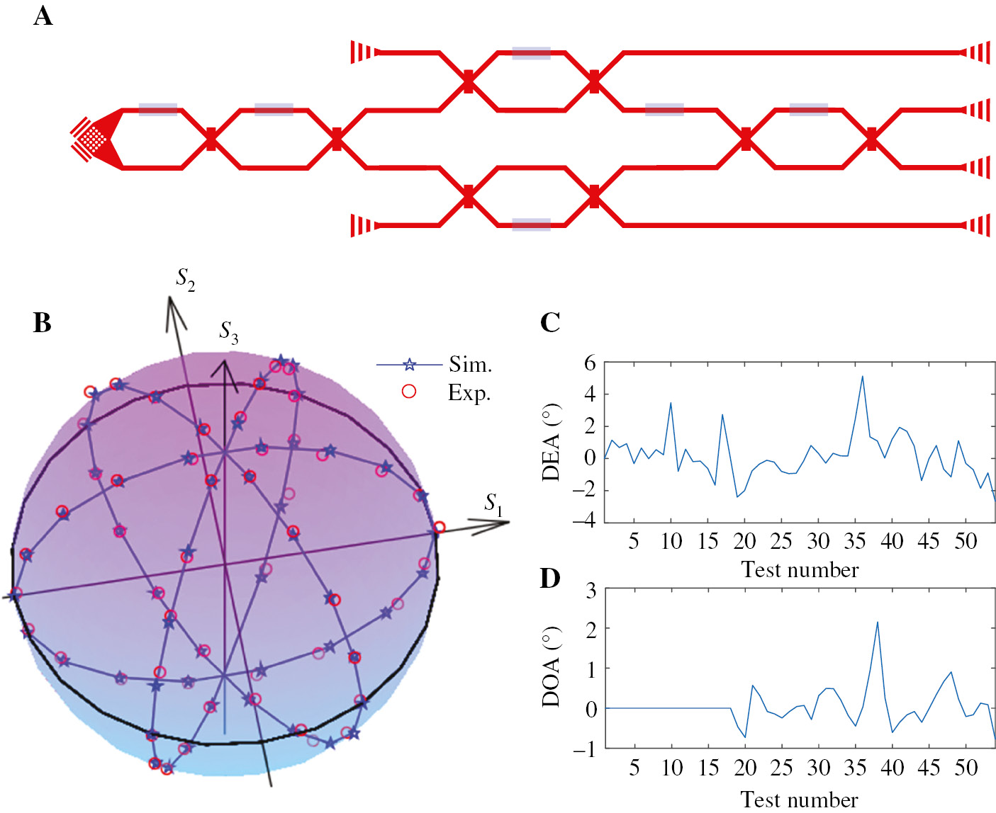
Experimental results for a division-of-space polarization analyzer.
(A) Used structure. (B) Experimental Stokes parameters compared with the theoretical results. (C) Deviations of the ellipticity angle. (D) Deviations of the orientation angle.
The deviations of the ellipticity angle (DEAs) and the deviations of the orientation angle (DOAs) are further analyzed, as shown in Figure 6C,D. The DEAs are changed from –2.7° to 5.1° and the DOAs are varied from –0.77° to 2.16°. The root-mean-squared errors (RMSEs) of DEAs and DOAs are 1.38° and 0.45°, respectively.
This chip can also implement a polarization analyzer with the division-of-time method. In this case, only the first MZI and Port 1 are utilized, as shown in Figure 7A. Four sets of random DC voltages are applied on the two phase shifters, and the output power of different polarized components is received at different times. The final experimental Stokes parameters are presented on the Poincaré sphere of Figure 7B, which are consistent with the theoretical results. The DEAs shown in Figure 7C are changed from –3.2° to 7.3°, and the DOAs shown in Figure 7D are varied from –2.1° to 2.2°. The RMSEs of DEAs and DOAs are 1.11° and 0.84°, respectively.
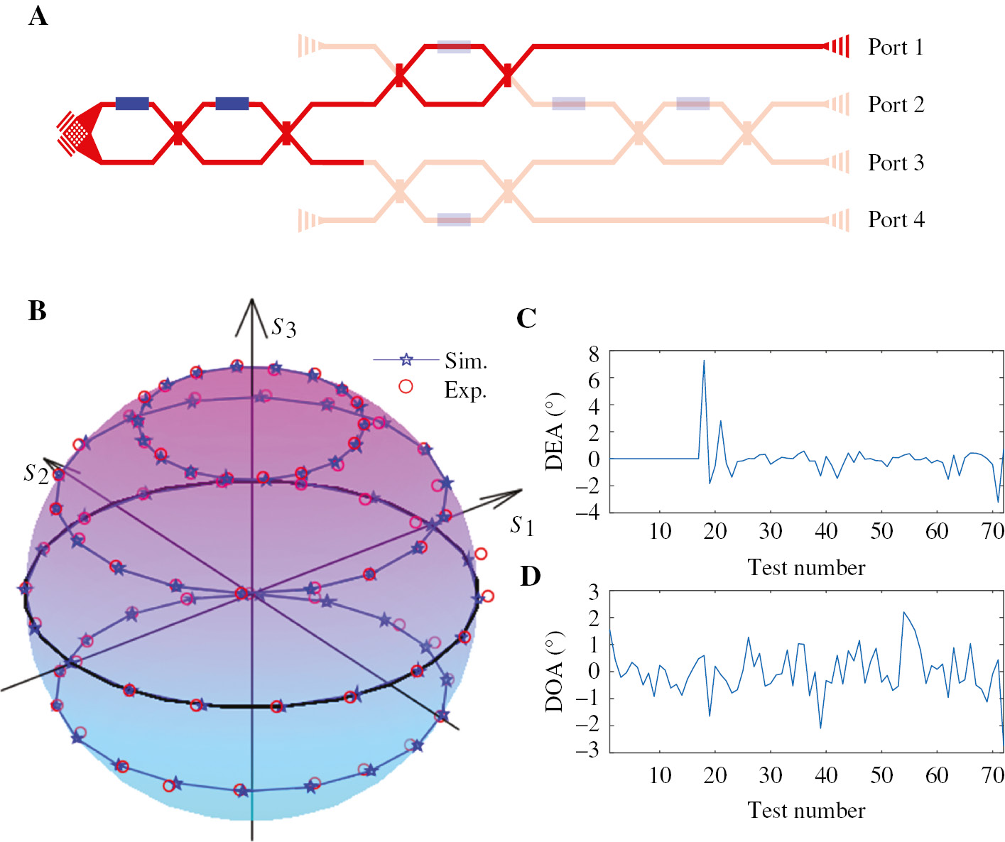
Experimental results for a division-of-time polarization analyzer.
(A) Used structure. (B) Experimental Stokes parameters compared with the theoretical results. (C) Deviations of the ellipticity angle. (D) Deviations of the orientation angle.
3.5 Potentials for more polarization processing
The proposed photonic polarization processor can perform multiple functions, including as a polarization MIMO descrambler, polarization controller, and polarization analyzer, which are basic building blocks in polarization processing. In fact, the polarization MIMO descrambler can cover the functions of polarization splitting, polarization multiplexing/demultiplexing, and polarization switching. Furthermore, arbitrary polarization-based coordinate conversion can be further performed if another symmetrical 2D grating is used to couple the light out from the chip, as shown in Figure 8. In the case, the polarization transformation can be expressed as
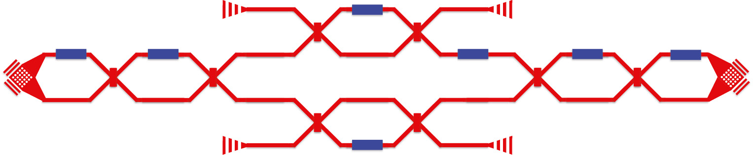
Photonic polarization processing circuits for polarization-based coordinate conversion.
Here, Pin, Qin are the input SOPs of two channels and Pout, Qout are the output SOPs. A WP or a PR can be realized when the transmission matrix is a unitary matrix (i.e., orthogonal coordinate conversion). And an arbitrary WP or PR can be designed by tuning the transmission matrix. Non-orthogonal coordinate conversion can be also performed if the transmission matrix is reversible but not unitary. It can be used to correct the SOPs of two channels provided the two channels degrade and become non-orthogonal. Finally, an arbitrary polarizer can be implemented when the transmission matrix is irreversible. For example, the light with SOP P⊥ is blocked by the chip and the light with SOP P can pass through the chip when M=[P, P]*; here the operation “*” means conjugate transposition. Up to now, we have demonstrated a variety of polarization processing functions with our chip, which cover almost all the basic building blocks of polarization processing, revealing the potential for an all-in-one photonic polarization processor.
4 Summary
In conclusion, we have designed, fabricated, and demonstrated an all-in-one, chip-scale polarization processor based on a linear optical network. By tuning the transmission matrix of the network, the chip can be configured as a polarization MIMO descrambler, a polarization controller, a division-of-space polarization analyzer, and a division-of-time polarization analyzer. A numerical gradient descent algorithm was employed to self-configure and self-optimize these functions. More functions can be configured, such as an arbitrary wave plate, PR, and polarizer, if another 2D grating is used to couple the light out from the chip. Our chip can achieve almost all the basic building blocks of polarization processing, suggesting great potential for chip-scale, reconfigurable, and fully programmable photonic polarization processing with the AI algorithm.
Acknowledgment
This work was partially supported by National Key Research and Development Project of China (2018YFB2201901), the National Natural Science Foundation of China (61622502, 61805090, Funder Id: http://dx.doi.org/10.13039/501100001809), the China Postdoctoral Science Foundation (2017M622419), the State Key Laboratory of Advanced Optical Communication Systems and Networks, Shanghai Jiao Tong University, China (2019GZKF03002), the Hong Kong Research Grants Council (PolyU152471/16E), and the Hong Kong Scholars Program 2018 (XJ2018018, Funder Id: http://dx.doi.org/10.13039/501100005953).
References
[1] Dai DX, Li CL, Wang SP, et al. 10-channel mode (de)multiplexer with dual polarizations. Laser Photon Rev 2018;12:1700109.10.1002/lpor.201700109Search in Google Scholar
[2] Wang J, He SL, Dai DX. On-chip silicon 8-channel hybrid (de) multiplexer enabling simultaneous mode-and polarization-division-multiplexing. Laser Photon Rev 2014;8:L18–22.10.1002/lpor.201300157Search in Google Scholar
[3] Chen Z-Y, Yan L-S, Pan Y, et al. Use of polarization freedom beyond polarization-division multiplexing to support high-speed and spectral-efficient data transmission. Light: Sci Appl 2016;6:e16207.10.1038/lsa.2016.207Search in Google Scholar PubMed PubMed Central
[4] Tyo JS, Goldstein DL, Chenault DB, Shaw JA. Review of passive imaging polarimetry for remote sensing applications. Appl Opt 2006;45:5453–69.10.1364/AO.45.005453Search in Google Scholar PubMed
[5] Ding D-S, Zhang W, Zhou ZY, Shi S, Shi B-S, Guo G-C. Raman quantum memory of photonic polarized entanglement. Nat Photon 2015;9:332.10.1038/nphoton.2015.43Search in Google Scholar
[6] Dai D, Bowers JE. Novel ultra-short and ultra-broadband polarization beam splitter based on a bent directional coupler. Opt Express 2011;19:18614–20.10.1364/OE.19.018614Search in Google Scholar PubMed
[7] Feng J, Zhou Z. Polarization beam splitter using a binary blazed grating coupler. Opt Lett 2007;32:1662–4.10.1364/OL.32.001662Search in Google Scholar PubMed
[8] Guan X, Wu H, Shi Y, Wosinski L, Dai D. Ultracompact and broadband polarization beam splitter utilizing the evanescent coupling between a hybrid plasmonic waveguide and a silicon nanowire. Opt Lett 2013;38:3005–8.10.1364/OL.38.003005Search in Google Scholar PubMed
[9] Lin J, Mueller JP, Wang Q, et al. Polarization-controlled tunable directional coupling of surface plasmon polaritons. Science 2013;340:331–4.10.1126/science.1233746Search in Google Scholar PubMed
[10] Dai D, Bowers JE. Novel concept for ultracompact polarization splitter-rotator based on silicon nanowires. Opt Express 2011;19:10940–9.10.1364/OE.19.010940Search in Google Scholar PubMed
[11] Alonso-Ramos C, Halir R, Ortega-Moñux A, et al. Highly tolerant tunable waveguide polarization rotator scheme. Opt Lett 2012;37:3534–6.10.1364/OL.37.003534Search in Google Scholar PubMed
[12] Wang ZC, Dai DX. Ultrasmall Si-nanowire-based polarization rotator. J Opt Soc Am B Opt Phys 2008;25:747–53.10.1364/JOSAB.25.000747Search in Google Scholar
[13] Rodríguez-Fortuño FJ, Puerto D, Griol A, Bellieres L, Martí J, Martínez A. Universal method for the synthesis of arbitrary polarization states radiated by a nanoantenna. Laser Photon Rev 2014;8:L27–31.10.1002/lpor.201300184Search in Google Scholar
[14] Velha P, Sorianello V, Preite MV, et al. Wide-band polarization controller for Si photonic integrated circuits. Opt Lett 2016;41:5656–9.10.1364/OL.41.005656Search in Google Scholar PubMed
[15] Sarmiento-Merenguel JD, Halir R, Le Roux X, et al. Demonstration of integrated polarization control with a 40dB range in extinction ratio. Optica 2015;2:1019.10.1364/OPTICA.2.001019Search in Google Scholar
[16] Kim J-W, Park S-H, Chu W-S, Oh M-C. Integrated-optic polarization controllers incorporating polymer waveguide birefringence modulators. Opt Express 2012;20:12443–8.10.1364/OE.20.012443Search in Google Scholar PubMed
[17] Zhou H, Yan S, Wei Y, et al. Silicon-based polarization analyzer by polarization-frequency mapping. APL Photon 2018;3:106105.10.1063/1.5044379Search in Google Scholar
[18] Espinosa-Soria A, Rodriguez-Fortuno FJ, Griol A, Martinez A. On-chip optimal stokes nanopolarimetry based on spin-orbit interaction of light. Nano Lett 2017;17:3139–44.10.1021/acs.nanolett.7b00564Search in Google Scholar PubMed
[19] Wu W, Yu Y, Liu W, Zhang X. Fully integrated CMOS-compatible polarization analyzer. Nanophotonics 2019;8:467–74.10.1515/nanoph-2018-0205Search in Google Scholar
[20] Rubin NA, Zaidi A, Juhl M, et al. Polarization state generation and measurement with a single metasurface. Opt Express 2018;26:21455–78.10.1364/OE.26.021455Search in Google Scholar PubMed
[21] Lin Z, Rusch L, Chen Y, Shi W. Chip-scale, full-Stokes polarimeter. Opt Express 2019;27:4867.10.1364/OE.27.004867Search in Google Scholar PubMed
[22] Alferness RC, Buhl L. Low-cross-talk waveguide polarization multiplexer/demultiplexer for λ=1.32 μm. Opt Lett 1984;9:140–2.10.1364/OL.9.000140Search in Google Scholar PubMed
[23] Doerr CR, Fontaine NK, Buhl LL. PDM-DQPSK silicon receiver with integrated monitor and minimum number of controls. IEEE Photon Technol Lett 2012;24:697–9.10.1109/LPT.2012.2187048Search in Google Scholar
[24] Li X, Zhong WD, Alphones A, Yu CY, Xu ZW. Channel equalization in optical OFDM systems using independent component analysis. J Lightwave Technol 2014;32:3206–14.10.1109/JLT.2014.2340431Search in Google Scholar
[25] Miller DA. Reconfigurable add-drop multiplexer for spatial modes. Opt Express 2013;21:20220–9.10.1364/OE.21.020220Search in Google Scholar PubMed
[26] Annoni A, Guglielmi E, Carminati M, et al. Unscrambling light – automatically undoing strong mixing between modes. Light: Sci Appl 2017;6:e17110.10.1038/lsa.2017.110Search in Google Scholar PubMed PubMed Central
[27] Melati D, Alippi A, Melloni A. Reconfigurable photonic integrated mode (de)multiplexer for SDM fiber transmission. Opt Express 2016;24:12625–34.10.1364/OE.24.012625Search in Google Scholar PubMed
[28] Koch B, Noe R, Sandel D, Mirvoda V. Versatile endless optical polarization controller/tracker/demultiplexer. Opt Express 2014;22:8259–76.10.1364/OE.22.008259Search in Google Scholar PubMed
[29] Lee K, Yun H, Mun SE, Lee GY, Sung J, Lee B. Ultracompact broadband plasmonic polarimeter. Laser Photon Rev 2018;12:1700297.10.1002/lpor.201700297Search in Google Scholar
[30] Balthasar Mueller JP, Leosson K, Capasso F. Ultracompact metasurface in-line polarimeter. Optica 2016;3:42–7.10.1364/OPTICA.3.000042Search in Google Scholar
[31] Pors A, Nielsen MG, Bozhevolnyi SI. Plasmonic metagratings for simultaneous determination of Stokes parameters. Optica 2015;2:716–23.10.1364/OPTICA.2.000716Search in Google Scholar
[32] Zhou H, Liu M, Dong J, Zhang X. Tomographic polarization analyzer by polarization-mode-frequency mapping. Opt Express 2017;25:14023–32.10.1364/OE.25.014023Search in Google Scholar PubMed
[33] Zhou HL, Fu DZ, Dong JJ, et al. Orbital angular momentum complex spectrum analyzer for vortex light based on the rotational Doppler effect. Light Sci Appl 2017;6: e16251.10.1038/lsa.2016.251Search in Google Scholar PubMed PubMed Central
[34] Carolan J, Harrold C, Sparrow C, et al. Quantum optics. Universal linear optics. Science 2015;349:711–6.10.1126/science.aab3642Search in Google Scholar PubMed
[35] Zhuang LM, Roeloffzen CGH, Hoekman M, Boller KJ, Lowery AJ. Programmable photonic signal processor chip for radiofrequency applications. Optica 2015;2:854–9.10.1364/OPTICA.2.000854Search in Google Scholar
[36] Perez D, Gasulla I, Crudgington L, et al. Multipurpose silicon photonics signal processor core. Nat Commun 2017;8:636.10.1038/s41467-017-00714-1Search in Google Scholar PubMed PubMed Central
[37] Harris NC, Carolan J, Bunandar D, et al. Linear programmable nanophotonic processors. Optica 2018;5:1623–31.10.1364/OPTICA.5.001623Search in Google Scholar
[38] Miller DAB. Self-configuring universal linear optical component [Invited]. Photon Res 2013;1:1–15.10.1364/PRJ.1.000001Search in Google Scholar
[39] Liu W, Li M, Guzzon RS, et al. A fully reconfigurable photonic integrated signal processor. Nat Photon 2016;10:190–5.10.1038/nphoton.2015.281Search in Google Scholar
[40] Clements WR, Humphreys PC, Metcalf BJ, Kolthammer WS, Walmsley IA. Optimal design for universal multiport interferometers. Optica 2016;3:1460–5.10.1364/OPTICA.3.001460Search in Google Scholar
[41] Hughes TW, Minkov M, Shi Y, Fan SH. Training of photonic neural networks through in situ backpropagation and gradient measurement. Optica 2018;5:864–71.10.1364/OPTICA.5.000864Search in Google Scholar
[42] Mennea PL, Clements WR, Smith DH, et al. Modular linear optical circuits. Optica 2018;5:1087–90.10.1364/OPTICA.5.001087Search in Google Scholar
[43] Miller DAB. Perfect optics with imperfect components. Optica 2015;2:747.10.1364/OPTICA.2.000747Search in Google Scholar
[44] Ribeiro A, Ruocco A, Vanacker L, Bogaerts W. Demonstration of a 4×4-port universal linear circuit. Optica 2016;3:1348–57.10.1364/OPTICA.3.001348Search in Google Scholar
[45] Reck M, Zeilinger A, Bernstein HJ, Bertani P. Experimental realization of any discrete unitary operator. Phys Rev Lett 1994;73:58–61.10.1103/PhysRevLett.73.58Search in Google Scholar PubMed
[46] Shen Y, Harris NC, Skirlo S, et al. Deep learning with coherent nanophotonic circuits. Nat Photon 2017;11:441–6.10.1038/nphoton.2017.93Search in Google Scholar
[47] Lin X, Rivenson Y, Yardimci NT, et al. All-optical machine learning using diffractive deep neural networks. Science 2018;361:1004–8.10.1126/science.aat8084Search in Google Scholar PubMed
Supplementary Material
The online version of this article offers supplementary material (https://doi.org/10.1515/nanoph-2019-0310).
© 2019 Jianji Dong et al., published by De Gruyter, Berlin/Boston
This work is licensed under the Creative Commons Attribution 4.0 Public License.
Articles in the same Issue
- Review Articles
- A review of 2D and 3D plasmonic nanostructure array patterns: fabrication, light management and sensing applications
- Semiconductor nanowire plasmonic lasers
- Fluorescence imaging with tailored light
- Phonon-polaritonics: enabling powerful capabilities for infrared photonics
- Research Articles
- All-optical vectorial control of multistate magnetization through anisotropy-mediated spin-orbit coupling
- CdSe/ZnS core-shell quantum dot assisted color conversion of violet laser diode for white lighting communication
- Improved near-UV electroluminescence of ZnO nanorod array LEDs by coupling with a graphene plasmon layer
- Promoting luminescence of Yb/Er codoped ferroelectric composite by polarization engineering for optoelectronic applications
- Two-dimensional Bi2S3-based all-optical photonic devices with strong nonlinearity due to spatial self-phase modulation
- Sub-terahertz and terahertz generation in long-wavelength quantum cascade lasers
- Iterative optimization of photonic crystal nanocavity designs by using deep neural networks
- All-in-one silicon photonic polarization processor
- Coulomb forces in THz electromechanical meta-atoms
- An electro-tunable Fabry–Perot interferometer based on dual mirror-on-mirror nanoplasmonic metamaterials
- Photonic bands, superchirality, and inverse design of a chiral minimal metasurface
- Grating-assisted coupling enhancing plasmonic tip nanofocusing illuminated via radial vector beam
- Greatly amplified spontaneous emission of colloidal quantum dots mediated by a dielectric-plasmonic hybrid nanoantenna
- Controllable Kerr and Raman-Kerr frequency combs in functionalized microsphere resonators
- Comprehensive insights into intracellular fate of WS2 nanosheets for enhanced photothermal therapeutic outcomes via exocytosis inhibition
- A new generation of dual-mode optical thermometry based on ZrO2:Eu3+ nanocrystals
- Corrigendum
- Corrigendum to: Dielectric cross-shaped-resonator-based metasurface for vortex beam generation at mid-IR and THz wavelengths