Improved near-UV electroluminescence of ZnO nanorod array LEDs by coupling with a graphene plasmon layer
-
Cen Zhang

 ,
Haiyang Xu
,
Liu Yang
,
Haiyang Xu
,
Liu Yang

Abstract
The development of short-wavelength light-emitting diodes (LEDs) with high emission efficiency, a fascinating research area, is still necessary because of great scientific interest and practical significance. Here, a graphene plasmon layer treated by oxygen plasma was employed into ZnO nanorod/p-GaN LEDs for a surface plasmon effect. The graphene-decorated heterojunction exhibited an approximately 4-fold improvement of ZnO ultraviolet (UV) electroluminescence (EL) intensity relative to a primitive p-n junction device. Time-resolved spectroscopy and temperature-dependent luminescence measurement indicated that the EL enhancement resulted from the coupling of ZnO excitons with graphene surface plasmons. The current research not only provides an opportunity to construct three-dimensional architecture from a vertical array of one-dimensional nanorods and a two-dimensional graphene layer, but also proposes an effective strategy to improve near-UV emission efficiency in various devices.
1 Introduction
A one-dimensional (1D) nanorod (NR) may be regarded as an ideal single crystal with superior photoelectric performance. Merging NRs into light-emitting diodes (LEDs) can effectively improve device performance [1], [2], [3], [4]. ZnO is a third-generation semiconductor that is a potential building block for short-wavelength LEDs [5], [6], [7], [8]. In particular, 1D ZnO NR arrays have exhibited excellent performance in the field of light-emitting devices [9], [10], [11], [12], [13], [14], [15], [16]. Recently, Chongxin Shan’s research groups used 1D ZnO micro-nano heterostructures for electrically pumped Fabry-Perot micro-lasers and electrically driven ultraviolet (UV) plasmonic lasers at room temperature [17], [18]. However, an increased surface-to-volume ratio deteriorates the efficiency and stability of ZnO NR LEDs. Thus, an important challenge is to overcome these surface-mediated non-radiative and deep-level recombination channels in order to improve device performance.
Surface plasmons (SPs) are electron oscillations that have attracted intense interest as a means to increase luminescence efficiency [19], [20], [21], [22]. Recently, graphitic carbon materials have exhibited a resonant SP effect attributed to an induced oscillation behavior of π and π+σ electrons with Dirac-cone-like energy bands [23], [24], [25], [26], [27], [28], [29]. Two-dimensional (2D) graphene, a layered structure of sp2-hybridized carbon atoms with a unique honeycomb lattice structure, has been of considerable interest because of the ability to engineer its band gap and the Fermi energy via electrical gating and carrier doping [30], [31]. As early as 2008, Nair et al. [32] reported for the first time that the unexpected absorption was attributed to the excitation of spectrally broadened surface plasmonic modes in graphene and the breakdown of the Dirac-fermion model, caused by triangular warping and non-linearity of energy bands far from the Dirac energy. Next, Dawlaty et al. [33] presented experimental results on the optical absorption spectra of epitaxial graphene from UV to the visible frequency range. Subsequently, Hwang et al. [24] also observed that the graphene showed an abnormally increased absorption in the violet-frequency region. They demonstrated that the resonant excitation of graphene plasmon is responsible for such absorption and eventually contributes to enhanced photoemission from structures of graphene/ZnO films when the corrugation of the ZnO surface modulates photons emitted from ZnO to fulfill the dispersion relation of graphene plasmon. Meanwhile, Koppens et al. [26] expounded a light-matter interaction process and optical field confinement induced by graphene. These important findings have unquestionably confirmed that graphene can show an abnormal absorption in the UV region, which indicated a probable SP effect. Furthermore, compared with metal SPs, graphene-like SPs are conveniently tunable in a wide spectral range and generally have lower optical loss, greater confinement, and better flexibility [25], [34]. These favorable factors promise greater resonant coupling and should stimulate the development of new optoelectronic devices. Therefore, graphene is now regarded as a more promising plasmonic material than metals. Additionally, versatile 2D graphene nano-materials have many advantages and unique characteristics, such as mechanical, electrical, and thermal stability; higher quantum efficiency; and strong non-linear optical processes. They have been used in plasmonic devices, information storage devices, and LEDs [34], [35]. Hence, there are significant scientific value and economic benefits in developing graphene-based LEDs with SP modulation. Resonant enhancement induced by graphene SPs and an increased ZnO luminescence have been demonstrated for the graphene/ZnO system. However, most reports focused on enhanced photoluminescence (PL) [36], [37], [38], [39], [40], [41], [42], [43], [44] rather than greater UV electroluminescence (EL) [45], [46].
Here, a hybrid 3D structure of 1D ZnO NR vertical arrays and a 2D graphene plasmon layer was fabricated on a commercial p-GaN substrate. By some effective means, the graphene plasmon layer was directly inserted into the active region between the NR arrays and the substrate, optimizing the SP-enhanced LED luminescence. Compared with the primitive ZnO/GaN heterostructure, the graphene-embedded device demonstrated an approximately 4-fold improvement in near-UV EL intensity. The enhancement mechanism was revealed according to time-resolved spectroscopy and temperature-dependent PL (TD-PL). The internal quantum efficiency (IQE) was estimated to be approximately 53%, which is among the highest reported for ZnO nanostructures. In our current study, by introducing a graphene plasmon layer, improved UV EL behavior was observed. To the best of our knowledge, this contribution may be the first to report on graphene-based SP-improved ZnO UV LEDs.
2 Experiments
Simple p-n heterostructure ZnO NR arrays were epitaxially prepared, as described previously [15], on commercial p-GaN substrates using a hydrothermal synthesis method. Catalysts and seed layers were not required, and zinc acetate and hexamethylenetetramine were used as precursors. The device structure and preparation were modified to investigate the effect of the embedded graphene plasmon layer on ZnO luminescence. Because the layer had to be near the active region to enhance the luminescence, it was transferred to the p-GaN substrate before growth of the ZnO NR arrays, as reported previously [47], [48]. Initially, polymethyl methacrylate (PMMA) was dissolved in acetone solution at a 4% mass fraction and spin-coated as a protective layer (3600 r/min, 30 s) on a graphene sheet supported on a Cu substrate. The sample was then placed on a 110°C heating plate for 15 min, followed by immersion in an FeCl3 solution to remove the Cu substrate. The graphene/PMMA layer was then transferred onto a p-GaN substrate by a lift-up process and dried in air for 12 h. The sample was again heated at 130°C for 30 min, and then placed in a 50°C acetone solution for 10 min to dissolve and remove the residual PMMA. Thus, a precise and controllable graphene plasmon layer transfer process was accomplished. Because of the graphene dangling bonds and the lattice mismatch with ZnO, plasma processing technology was performed. Specifically, the graphene plasmon layer was placed in 100 Pa oxygen plasma for 1 min at an input power of 40 W to form dangling bonds and nucleation sites favorable to ZnO NR growth. This created oxygen-containing functional groups or defect sites on the surface of graphene for nucleation and growth of oxides, similar to the nitrogen plasma etching used for inorganic nitride growth (e.g. AlN and GaN) on graphene monolayers. High-performance blue LEDs were fabricated with these graphene-buffered nitride emissive layers [49], [50], [51], [52]. ZnO NR arrays were then synthesized on the graphene plasmon layer via the hydrothermal method noted above. A schematic of the fabrication procedure is shown in Figure 1. A primitive reference ZnO NR array/p-GaN LED without graphene plasmon layer decoration was also fabricated for comparison. Au/Ni and In contact electrodes were thermally evaporated on p-GaN and ZnO NR, respectively. PL and EL spectra were recorded and collected from one side of the cathode and detected in the same way for direct comparison.

Schematic of graphene transfer and device preparation process.
3 Results and discussion
ZnO NR arrays were synthesized on the commercial p-GaN chip or the graphene/p-GaN substrate was imaged with a scanning electron microscope (SEM), as shown in Figure 2A and B. The NRs were vertically aligned on the p-GaN substrates in a highly ordered distribution. The average NR diameter was approximately 150 nm and the average length was approximately 2 μm. The inset of Figure 2A is a high-magnification SEM image of a single ZnO NR having a flat and smooth side surface. After inserting the oxygen-plasma-processed graphene plasmon layer, the mass and morphology of the ZnO NR arrays did not degrade significantly and the surface density slightly decreased. In Figure 2C and D, the microstructure of a single ZnO NR was imaged with high-resolution transmission electron microscope (HRTEM) and selected-area electron diffraction (SAED). The SAED pattern was along the [011̅0] zone axis, indicating a single-crystal wurtzite structure with a [0002] growth direction. Interplanar spacings of 0.26 and 0.16 nm, corresponding to the orthogonal (0002) and (21̅1̅0) planes of wurtzite ZnO, were clearly observed. Furthermore, superimposed electronic images and energy dispersive X-ray (EDX) mapping of a single ZnO NR on graphene-covered p-GaN (inset of Figure 2A) are shown in Figure 2E–J. They verified the uniform distributions of elemental Zn, O, Ga, N, and C.
![Figure 2: Microstructure characterization of the device.SEM images of ZnO NR arrays prepared on p-GaN substrates without (A) and with (B) graphene plasmon layer insertion. The inset of (A) shows a single smooth ZnO NR. (C) TEM image of ZnO NR. The inset displays the SAED pattern along the [011̅0] zone axis of a wurtzite structure. (D) HRTEM image with clear lattice fringes showing interplanar spacings of 0.26 and 0.16 nm, corresponding to the orthogonal (0002) and (21̅1̅0) planes of wurtzite ZnO. (E–J) EDX mapping results of single ZnO NR on graphene-covered p-GaN substrate.](/document/doi/10.1515/nanoph-2019-0228/asset/graphic/j_nanoph-2019-0228_fig_002.jpg)
Microstructure characterization of the device.
SEM images of ZnO NR arrays prepared on p-GaN substrates without (A) and with (B) graphene plasmon layer insertion. The inset of (A) shows a single smooth ZnO NR. (C) TEM image of ZnO NR. The inset displays the SAED pattern along the [011̅0] zone axis of a wurtzite structure. (D) HRTEM image with clear lattice fringes showing interplanar spacings of 0.26 and 0.16 nm, corresponding to the orthogonal (0002) and (21̅1̅0) planes of wurtzite ZnO. (E–J) EDX mapping results of single ZnO NR on graphene-covered p-GaN substrate.
The EDX patterns (Figure 3A) collected from the surface of the microstructure also indicated the formation of a heterostructure. The X-ray diffraction pattern depicted in Figure 3B, which included (100), (002), (101), (102), (110), (103), (200), and (004) planes, matched well with Joint Committee on Powder Diffraction Standard card no. 36-1451. The sample prepared on graphene-covered p-GaN had a higher-intensity (002) peak, which implied a vertical alignment consistent with the SEM images in Figure 2A and B. A Raman spectrum of transferred graphene (red line in Figure 3C) had two vibrations at 1580 and 2700 cm−1 attributed to the G and 2D bands, respectively. The 2D/G intensity ratio was 2.4, which indicated good-quality layered graphene [53], [54]. Raman spectroscopy of the sample after oxygen plasma treatment (blue line in Figure 3C) exhibited a stronger D peak (ID) and a weaker G peak (IG), enhancing the ID/IG ratio and indicating that the perfect graphene structure was degraded. This indirectly verified changes in the defect density (point-like defects and nucleation sites) to enable growth of ZnO NR arrays [55]. Cancado et al. and Lucchese et al. carried out theoretical quantitative analysis and proposed that the defect density was closely related to ID/IG. The relationship can be represented by [56], [57]:

The structure and optical properties in both devices.
(A) EDX pattern collected from the graphene-decorated ZnO NR array/p-GaN. (B) XRD pattern of graphene-decorated ZnO NR prepared on a p-GaN substrate. The curve at the bottom is the standard Powder Diffraction File (PDF) card for ZnO lattice structure. (C) Raman characterization of a graphene plasmon layer before (red curve) and after (blue curve) oxygen plasma treatment. (D) PL measurement of ZnO NR array/p-GaN without (red line) and with (blue line) graphene plasmon layer decoration.
The length scales of rA and rS indicated the region around D band scattering, where rS is the radius of a disordered area, rA is the radius of a point defective area, and LD is the distance between point-like defects. Studies have shown that ID/IG is dependent on the activated area, which is weighted by the parameter CA, and a defective area weighted by the parameter CS [53]. Herein, we chose CS=0 and
By replacing rA=3.1 nm, rS=1 nm, Eq. (2) can be rewritten as
According to the wavelength of the laser excitation λL, we obtain
Finally, according to Eqs. (3) and (4), the expression for the defect density is
and
From the Raman spectra of the graphene plasmon layer before and after oxygen plasma treatment, the values of ID/IG (before),
Figure 4A displays a structural diagram of the graphene-inserted ZnO NR array/p-GaN heterojunction LED. As described in Section 2 the graphene plasmon layer was introduced without affecting the original heterostructure. A primitive ZnO NR array/p-GaN LED was also constructed, and the performances of both LEDs were characterized. As shown in Figure 4B, the current-versus-voltage (I–V) curves of both junctions exhibited good rectification behavior, which indicated that the graphene plasmon layer did not significantly degrade longitudinal electrical transport. More important, the inserted graphene device had lower forward-injection and reverse-leakage currents at the same voltage, which resulted from the increased series resistance. Additionally, the ohmic contact between the positive electrode (Au/Ni) and p-GaN was acceptable, as shown by the linear I–V curve in the inset of Figure 4B (orange triangles). Negative electrode In easily formed an ideal ohmic contact with ZnO, which was also demonstrated by a linear I–V curve (green squares in the inset). We considered that this graphene plasmon layer also has other advantages during device operation. For example, it has a good heat dissipation layer that allows the heat to spread from the ZnO NR arrays to the p-GaN, reducing the junction temperature. It may promote the radiative recombination of ZnO excitons and probably leads to higher UV emission. Moreover, the oxygen-plasma-processed graphene plasmon layer is a less-conductive semi-insulating blocking layer that slows down the diffusion of electrons from the ZnO NR arrays to p-GaN, which enables ZnO UV luminescence. Overall, introducing the graphene plasmon layer is likely to produce better device performance.

(A) Device structure diagram of graphene-decorated ZnO NR array/p-GaN heterojunction. (B) I–V curves of both devices without and with a graphene plasmon layer.
The inset shows the near-linear I–V characters of Au/Ni-p-GaN and In-ZnO NR arrays, confirming good ohmic contacts.
In Figure 5A and B, there are two sets of EL spectra obtained under a forward bias from ZnO NR array/p-GaN heterojunctions without and with graphene plasmon layer decoration. With the injection current ranging from 1 to 10 mA, both EL spectra exhibited a broad near-UV emission band, which may have included several luminescence sources and increased in intensity with injection current. The most striking feature in Figure 5A and B was that the LED with the embedded graphene plasmon layer had much stronger near-UV luminescence centered at approximately 395 nm. The integrated intensities of both heterojunctions as a function of injection current are shown in Figure 5C. The intensities of both LEDs increased with injection current and saturated near 10 mA. The inset of Figure 5C shows a change rule between the enhancement ratio and injection current. The ratio gradually decreased and leveled off at approximately 1.0 when the injection current reached 10 mA. This was most likely because Joule heating became more dominant at higher injection currents and also because of the screening effect of excess carriers induced by higher injection levels for the SP-enhanced LEDs. The above discussion indicated a more appreciable enhancement observed at lower injection levels. Therefore, both EL measurements detected at 1 mA acted as the objects of the study for comparison. In Figure 5D, the main difference was that the intensity of the graphene-inserted heterojunction was more than approximately 4 times that of the primitive ZnO NR array/p-GaN LED device, as reflected in the EL photographs. Moreover, the broad-band near-UV emission peak position experienced no red shift in the EL spectra.

EL spectra of both LEDs (A) without and (B) with graphene plasmon layer decoration, collected at the front of the devices for variable injection currents from 1 to 10 mA. (C) Relationship among integral intensity, improvement ratio, and injection current. (D) EL measurement of light-emitting devices without and with a graphene plasmon layer collected at an applied current of 1 mA.
The insets show instant EL photographs.
A traditional ZnO/GaN heterojunction can generally produce several luminescence sources, as demonstrated by the broad-band EL spectra. To better analyze and recognize the changes in the spectral lines, both spectra were analyzed with Gaussian deconvolution fits in Figure 6A and B. The applied current was fixed at 1 mA, and defect-related ZnO emissions were very weak. Therefore, the EL broad-band emissions from the two LEDs were split into three independent types of recombination. According to previous reports and the aforementioned PL characterization, these emission peaks were reasonably given to ZnO excitonic radiative recombination, interfacial recombination, and Mg-acceptor dependent emission in p-GaN [8], [9], [10]. All spectra from the primitive ZnO NR array/p-GaN LED derived from pronounced ZnO excitonic emission and interfacial recombination, while the p-GaN acceptor emission accounted for a relatively small proportion, as seen in the weight distribution in Figure 6A. However, after inserting the graphene plasmon layer, the components of decomposed sub-peaks greatly improved (Figure 6B) because of the spectral overlap between the near-UV luminescence and the increased abnormal absorption of graphene in the UV region. Additionally, the weight and enhancement of each sub-peak were changed observably, as described in Figure 6C and D. Similar to PL enhancement, the ZnO excitonic emission was effectively enhanced by approximately 4-fold. The increased abnormal absorption of graphene suggested that its SP resonance frequency was mainly situated in the UV region. Therefore, there was a near-UV emission enhancement from the ZnO NR arrays.

The luminescence sources in EL spectra.
Gaussian deconvolution fittings of EL spectra in LEDs without (A) and with (B) a graphene plasmon layer. (C) Weight distribution of every luminescence component. (D) Enhancement ratio of every luminescence component.
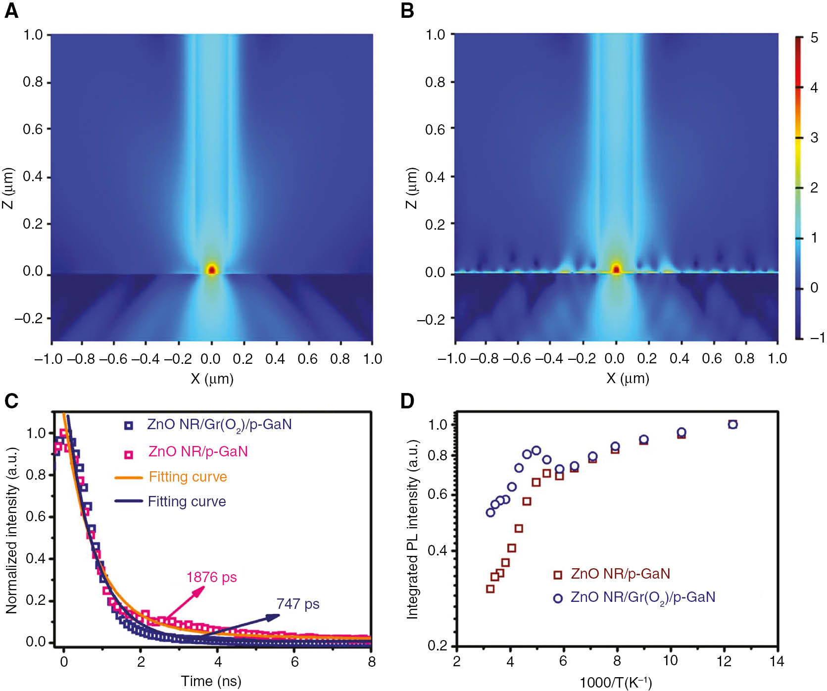
As expected from a plasmonic material, graphene SP can also provide an additional radiative recombination route, which can improve the IQE. The energy of some particles, such as electron-hole pairs/excitons in semiconductors, can be coupled to an SP mode and then scattered into free space radiatively. It has been proposed that SP can be generated on the surface of a graphene plasmon layer in a driven heterojunction LED, which has a great effect on luminescence enhancement. To demonstrate this proposal, finite-difference time-domain (FDTD) numerical simulations were performed on the spatial distributions of the electric field intensity at the ZnO NR array/p-GaN interface without and with graphene. The simulation model construction and parameter selections resembled the actual device configuration to ensure reliability. A dipole light source was situated in the junction area, i.e. in accordance with the active region. As presented in Figure 7A and B, the simulations first suggested that the luminescence can be rather confined to the active region and propagate along the NR growth direction, which has been previously confirmed in waveguide-type transmission and light-emitting modes [15]. Further, the SP effect similar to a surface propagation plasmon can be generated on the surface of a graphene plasmon layer, and the graphene enables the energy of light to spread horizontally. Finally, the FDTD results demonstrated that graphene in the active region clearly improved the emitted luminescence intensity of an individual ZnO NR. For ZnO NR array/p-GaN heterojunction, its EL enhancement originates from the collective effect of luminescence improvement of individual ZnO NR. In fact, Chunxiang Xu’s groups have reported some related works on graphene-improved ZnO UV emission [30], [32], [34], [36], [37]. Especially, some interesting works have been focused on numerical simulation of graphene/ZnO heterostructures [36], [60]. These works indicated that the graphene SP can be located in the UV frequency region and couple with ZnO excitons to generate ZnO UV luminescence enhancement.
Graphene plasmonic effect.
FDTD simulations of electric field intensity spatial distributions at a ZnO NR array/p-GaN interface (A) without and (B) with graphene plasmon layer decoration. (C) TR-PL measurements of both heterojunctions. (D) Arrhenius plots of the normalized intensity from ZnO NR arrays without (red squares) and with (blue circles) graphene plasmon layer decoration.
Another way to understand this phenomenon is that the light source of energy can be coupled with the excited graphene SP, which indicates the existence of a resonance coupling interaction between graphene SP and ZnO exciton. To verify this proposal, time-resolved PL (TR-PL) was performed with a fluorescence measurement system (Photon Technology International, London, Ontario, Canada), a pulsed laser of nitrogen molecule, and a photomultiplier. ZnO UV emission at 377 nm was monitored. In Figure 7C, fluorescence decay curves with and without the graphene plasmon layer are illustrated. The curves were normalized and fit to bi-exponential functions. The effective PL lifetimes for the graphene-decorated structure and the pure ZnO NR were determined to be approximately 747 and 1876 ps, respectively. The graphene-decorated ZnO NR array/p-GaN exhibited a faster spontaneous radiative recombination rate than that of the primitive heterostructure, indicating exciton-SP resonant coupling and an increased IQE. To further confirm the latter, TD-PL spectra were acquired over the temperature range 85–310 K. Figure 7D displays Arrhenius plots of UV integrated intensity for ZnO NRs without and with graphene decoration. Interestingly, the graphene-inserted structure presented slower temperature quenching than the primitive structure. Thus, its IQE increased from 30% to 53% via exciton-SP resonant coupling. Herein, it is noteworthy that the IQE of graphene SP-decorated ZnO NR array reaches approximately 53%, which is among the highest reported for ZnO nanostructures. In addition, there was an anomalous change in the integrated intensity over the temperature range 170–230 K in both structures. This was because bound excitons in the surface or interface states were thermally dissociated into free excitons, which provide newly created energy for UV luminescence [61], [62]. More detailed TR-PL and TD-PL characteristics have been previously reported [8], [15], [16]. These experimental results verified the origin of the luminescence enhancement.
The spatial distribution of the light output in the light-emitting device is as important as the emission efficiency. The angle-resolved and normalized EL intensities from the LEDs without and with graphene plasmon layer were thus acquired. The inset of Figure 8A shows a structural diagram with respect to the angle-resolved EL configuration used for data acquisition. The primitive LED exhibited high light output directionality because of the waveguide model. The EL had maximum intensity along the growth direction and decayed rapidly with increased angle. In contrast, the LED device with the graphene plasmon layer exhibited a broader angular distribution in Figure 8B. The width of the spatial distribution was extended, and the spatial uniformity was improved. The luminescence from the active region was divergent; however, the excited graphene SPs coupled with photons in the axial direction of the NRs. Hence, wasted photon energy was re-extracted by the SP mode and uniformly scattered into all directions, resulting in increased light extraction.

Measured angle-resolved integral intensities of both LEDs in (A) rectangular coordinates and (B) polar coordinates.
The curves are normalized by the axial direction EL intensity.
4 Conclusions
A near-UV nano-LED was fabricated according to procedures for ZnO NR/p-GaN junctions. When a graphene plasmon layer was introduced into the active region, there was a significant increase in ZnO UV PL and EL relative to the primitive device. This resulted from resonance coupling interaction between graphene SPs and ZnO excitons. The IQE of graphene-decorated ZnO NR array was approximately 53%, which is among the maximum values ever reported for ZnO nanostructures. Although the device structure should be redesigned and optimized, the current consideration of preparing graphene-decorated SP structures provide a novel approach for performance improvement for various LED devices.
Funding source: National Natural Science Foundation of China
Award Identifier / Grant number: 51732003
Award Identifier / Grant number: 51872043
Award Identifier / Grant number: 61604037
Award Identifier / Grant number: 11874104
Funding source: “111” Project
Award Identifier / Grant number: B13013
Funding source: Jilin Province
Award Identifier / Grant number: JJKH20180007KJ
Award Identifier / Grant number: JJKH20190274KJ
Funding source: Central Universities
Award Identifier / Grant number: 2412019BJ006
Award Identifier / Grant number: 2412019FZ034
Funding statement: Cen Zhang and Yue Qiu contributed equally to this work. This work was supported by the Program of National Natural Science Foundation of China (Funder Id: http://dx.doi.org/10.13039/501100001809, nos. 51732003, 51872043, 61604037, and 11874104), the “111” Project (no. B13013), the Fund from Jilin Province (nos. JJKH20180007KJ and JJKH20190274KJ), and the Fundamental Research Funds for the Central Universities (nos. 2412019BJ006 and 2412019FZ034).
References
[1] Li RX, Wei ZP, Zhao FH, et al. Investigation of localized and delocalized excitons in ZnO/ZnS core-shell heterostructured nanowires. Nanophotonics 2017;6:1093–110.10.1515/nanoph-2016-0157Suche in Google Scholar
[2] Zhang C, Qian QY, Qin LL, et al. Broadband light harvesting for highly efficient hot-electron application based on conformal metallic nanorod arrays. ACS Photon 2018;5:5079–85.10.1021/acsphotonics.8b01389Suche in Google Scholar
[3] Chou MC, Lin CY, Lin BL, et al. Polarization-selecting III-nitride elliptical nanorod light-emitting diodes fabricated with nanospherical-lens lithography. ACS Nano 2018;12:8748–57.10.1021/acsnano.8b04933Suche in Google Scholar PubMed
[4] Robin Y, Bae SY, Shubina TV, et al. Insight into the performance of multi-color InGaN/GaN nanorod light emitting diodes. Sci Rep 2018;8:7311–8.10.1038/s41598-018-25473-xSuche in Google Scholar PubMed PubMed Central
[5] Zhu H, Shan CX, Yao B, et al. Ultralow-threshold laser realized in zinc oxide. Adv Mater 2009;21:1613–7.10.1002/adma.200802907Suche in Google Scholar
[6] Chu S, Wang G, Zhou W, et al. Electrically pumped waveguide lasing from ZnO nanowires. Nat Nanotechnol 2011;6:506–10.10.1038/nnano.2011.97Suche in Google Scholar PubMed
[7] Zhang TF, Wu GA, Wang JZ, et al. A sensitive ultraviolet light photodiode based on graphene-on-zinc oxide Schottky junction. Nanophotonics 2017;6:1073–81.10.1515/nanoph-2016-0143Suche in Google Scholar
[8] Yang L, Liu WZ, Xu HY, et al. Enhanced near-UV electroluminescence from p-GaN/i-Al2O3/n-ZnO heterojunction LEDs by optimizing the insulator thickness and introducing surface plasmons of Ag nanowires. J Mater Chem C 2017;5:3288–95.10.1039/C7TC00419BSuche in Google Scholar
[9] Xu S, Xu C, Liu Y, et al. Ordered nanowire array blue/near-UV light emitting diodes. Adv Mater 2010;22:4749–53.10.1002/adma.201002134Suche in Google Scholar PubMed
[10] Dai J, Xu CX, Sun XW. ZnO-Microrod/p-GaN heterostructured whispering-gallery-mode microlaser diodes. Adv Mater 2011;23:4115–9.10.1002/adma.201102184Suche in Google Scholar PubMed
[11] Lu YJ, Shan CX, Zhou ZX, et al. Electrically pumped random lasers with p-diamond as a hole source. Optica 2015;2:558–62.10.1364/OPTICA.2.000558Suche in Google Scholar
[12] Zhao X, Gao Y, Wang Y, et al. Manipulating optical properties of ZnO/Ga:ZnO core-shell nanorods via spatially tailoring electronic bandgap. Adv Optical Mater 2015;3:1066–71.10.1002/adom.201500087Suche in Google Scholar
[13] Ren XL, Zhang XH, Liu NS, et al. White light-emitting diode from Sb-doped p-ZnO nanowire arrays/n-GaN film. Adv Funct Mater 2015;25:2182–8.10.1002/adfm.201404316Suche in Google Scholar
[14] Kwon OH, Jang JW, Park SJ, et al. Plasmonic-enhanced luminescence characteristics of microscale phosphor layers on a ZnO nanorod-arrayed glass substrate. ACS Appl Mater Interfaces 2019;11:1004–12.10.1021/acsami.8b13767Suche in Google Scholar PubMed
[15] Zhang C, Marvinney CE, Xu HY, et al. Enhanced waveguide-type ultraviolet electroluminescence from ZnO/MgZnO core/shell nanorod array light-emitting diodes via coupling with Ag nanoparticles localized surface plasmons. Nanoscale 2015;7:1073–80.10.1039/C4NR04966GSuche in Google Scholar PubMed
[16] Liu WZ, Xu HY, Yan SY, et al. Effect of SiO2 spacer-layer thickness on localized surface plasmon-enhanced ZnO nanorod array LEDs. ACS Appl Mater Interfaces 2016;8:1653–60.10.1021/acsami.5b08382Suche in Google Scholar PubMed
[17] Li Z, Jiang M, Sun Y, et al. Electrically pumped Fabry-Perot microlasers from single Ga-doped ZnO microbelt based heterostructure diodes. Nanoscale 2018;10:18774–85.10.1039/C8NR05559ASuche in Google Scholar PubMed
[18] Yang X, Ni PN, Jing PT, et al. Room temperature electrically driven ultraviolet plasmonic lasers. Adv Opt Mater 2019;7:1801681.10.1002/adom.201801681Suche in Google Scholar
[19] Okamoto K, Niki I, Shvartser A, et al. Surface-plasmon-enhanced light emitters based on InGaN quantum wells. Nat Mater 2004;3:601–5.10.1038/nmat1198Suche in Google Scholar PubMed
[20] Kim BH, Cho CH, Mun JS, et al. Enhancement of the external quantum efficiency of a silicon quantum dot light-emitting diode by localized surface plasmons. Adv Mater 2008;20:3100–4.10.1002/adma.200703096Suche in Google Scholar
[21] Zhang SG, Zhang XW, Yin ZG, et al. Localized surface plasmon-enhanced electroluminescence from ZnO-based heterojunction light-emitting diodes. Appl Phys Lett 2011;99:181116.10.1063/1.3658392Suche in Google Scholar
[22] Xu CX, Qin FF, Zhu QX, et al. Plasmon-enhanced ZnO whispering-gallery mode lasing. Nano Res 2018;11:3050–64.10.1007/s12274-018-2047-3Suche in Google Scholar
[23] Grigorenko AN, Polini M, Novoselov KS. Graphene plasmonics. Nat Photonics 2012;6:749–58.10.1038/nphoton.2012.262Suche in Google Scholar
[24] Hwang SW, Shin DH, Kim CO, et al. Plasmon-enhanced ultraviolet photoluminescence from hybrid structures of graphene/ZnO Films. Phys Rev Lett 2010;105:127403.10.1103/PhysRevLett.105.127403Suche in Google Scholar PubMed
[25] Guo DY, Shan CX, Liu KK, et al. Surface plasmon effect of carbon nanodots. Nanoscale 2015;7:18908–13.10.1039/C5NR05918FSuche in Google Scholar PubMed
[26] Koppens FHL, Chang DE, Abajo FJG. Graphene plasmonics: a platform for strong light-matter interactions. Nano Lett 2011;11:3370–7.10.1021/nl201771hSuche in Google Scholar PubMed
[27] Huang SY, Song CY, Zhang GW, et al. Graphene plasmonics: physics and potential applications. Nanophotonics 2017;6:1191–204.10.1515/nanoph-2016-0126Suche in Google Scholar
[28] Kuzmin DA, Bychkov IV, Shavrov VG, et al. Plasmonics of magnetic and topological graphene-based nanostructures. Nanophotonics 2018;7:597–611.10.1515/nanoph-2017-0095Suche in Google Scholar
[29] Shen CL, Lou Q, Lv CF, et al. Bright and multicolor chemiluminescent carbon nanodots for advanced information encryption. Adv Sci 2019;6:1802331.10.1002/advs.201802331Suche in Google Scholar PubMed PubMed Central
[30] Zhang YB, Tang TT, Girit C, et al. Direct observation of a widely tunable bandgap in bilayer graphene. Nature 2009;459:820–3.10.1038/nature08105Suche in Google Scholar PubMed
[31] Wang F, Zhang YB, Tian CS, et al. Gate-variable optical transitions in graphene. Science 2008;320:206–9.10.1126/science.1152793Suche in Google Scholar PubMed
[32] Nair RR, Blake P, Grigorenko AN, et al. Fine structure constant defines visual transparency of graphene. Science 2008;320:1308.10.1126/science.1156965Suche in Google Scholar PubMed
[33] Dawlaty JM, Shivaraman S, Strait J, et al. Measurement of the optical absorption spectra of epitaxial graphene from terahertz to visible. Appl Phys Lett 2008;93:131905.10.1063/1.2990753Suche in Google Scholar
[34] Luo XG, Qiu T, Lu WB, et al. Plasmons in graphene: recent progress and applications. Mater Sci Eng R 2013;74:351–76.10.1016/j.mser.2013.09.001Suche in Google Scholar
[35] Yan YB, Gong J, Chen J, et al. Recent advances on graphene quantum dots: from chemistry and physics to applications. Adv Mater 2019;31:1808283.10.1002/adma.201808283Suche in Google Scholar PubMed
[36] Liu R, Fu XW, Meng J, et al. Graphene plasmon enhanced photoluminescence in ZnO microwires. Nanoscale 2013;5:5294–8.10.1039/c3nr01226cSuche in Google Scholar PubMed
[37] Li JT, Lin Y, Lu JF, et al. Single mode ZnO whispering-gallery submicron cavity and graphene improved lasing performance. ACS Nano 2015;9:6794–800.10.1021/acsnano.5b01319Suche in Google Scholar PubMed
[38] Kim S, Shin DH, Kim CO, et al. Enhanced ultraviolet emission from hybrid structures of single-walled carbon nanotubes/ZnO films. Appl Phys Lett 2009;94:213113.10.1063/1.3148646Suche in Google Scholar
[39] Li JT, Xu CX, Nan HY, et al. Graphene surface plasmon induced optical field confinement and lasing enhancement in ZnO whispering-gallery microcavity. ACS Appl Mater Interfaces 2014;6:10469–75.10.1021/am502043fSuche in Google Scholar PubMed
[40] Kim K, Lee SM, Do YS, et al. Enhanced photoluminescence from zinc oxide by plasmonic resonance of reduced graphene oxide. J Appl Phys 2013;114:074903.10.1063/1.4818953Suche in Google Scholar
[41] Qin FF, Xu CX, Zhu QX, et al. Optical performance improvement in hydrothermal ZnO/graphene structures for ultraviolet lasing. J Mater Chem C 2018;6:3240–4.10.1039/C7TC05880BSuche in Google Scholar
[42] Han F, Yang SM, Jing WX, et al. Surface plasmon enhanced photoluminescence of ZnO nanorods by capping reduced graphene oxide sheets. Opt Express 2014;22:11436–45.10.1364/OE.22.011436Suche in Google Scholar PubMed
[43] Li JT, Jiang MM, Xu CX, et al. Plasmon coupled Fabry-Perot lasing enhancement in graphene/ZnO hybrid microcavity. Sci Rep 2015;8:9263.10.1038/srep09263Suche in Google Scholar PubMed PubMed Central
[44] Zhu QX, Qin FF, Lu JF, et al. Synergistic graphene/aluminum surface plasmon coupling for zinc oxide lasing improvement. Nano Res 2017;10:1996–2004.10.1007/s12274-016-1387-0Suche in Google Scholar
[45] Lee JM, Yi J, Lee WW, et al. ZnO nanorods-graphene hybrid structures for enhanced current spreading and light extraction in GaN-based light emitting diodes. Appl Phys Lett 2012;100:061107.10.1063/1.3683484Suche in Google Scholar
[46] Zhang C, Zhu FF, Xu HY, et al. Significant improvement of near-UV electroluminescence from ZnO quantum dot LEDs via coupling with carbon nanodot surface plasmons. Nanoscale 2017;9:14592–601.10.1039/C7NR04392ASuche in Google Scholar PubMed
[47] Barin GB, Song Y, Gimenez IF, et al. Optimized graphene transfer: Influence of polymethylmethacrylate (PMMA) layer concentration and baking time on graphene final performance. Carbon 2015;84:82–90.10.1016/j.carbon.2014.11.040Suche in Google Scholar
[48] Regan W, Alem N, Aleman B, et al. A direct transfer of layer-area graphene. Appl Phys Lett 2010;96:113102.10.1063/1.3337091Suche in Google Scholar
[49] Chung K, Beak H, Tchoe Y, et al. Growth and characterizations of GaN micro-rods on graphene films for flexible light emitting diodes. APL Mater 2014;2:092512.10.1063/1.4894780Suche in Google Scholar
[50] Chen ZL, Zhang X, Dou ZP, et al. High-brightness blue light-emitting diodes enabled by a directly grown graphene buffer layer. Adv Mater 2018;30:1801608.10.1002/adma.201801608Suche in Google Scholar PubMed
[51] Chen ZL, Liu ZQ, Wei TB, et al. Improved epitaxy of AlN film for deep-ultraviolet light-emitting diodes enabled by graphene. Adv Mater 2019;31:1807345.10.1002/adma.201807345Suche in Google Scholar PubMed
[52] Ci HN, Chang HL, Wang RY, et al. Enhancement of heat dissipation in ultraviolet light-emitting diodes by a vertically oriented graphene nanowall buffer layer. Adv Mater 2019;31:1901624.10.1002/adma.201901624Suche in Google Scholar PubMed
[53] Wimalananda MDSL, Kim JK, Lee JM. Effect of annealing dependent surface free energy change of Cu foil during graphene growth on quality of monolayer continuous graphene. Carbon 2016;108:127–34.10.1016/j.carbon.2016.07.006Suche in Google Scholar
[54] Ni ZH, Wang YY, Yu T, et al. Raman spectroscopy and imaging of graphene. Nano Res 2008;1:273–91.10.1007/s12274-008-8036-1Suche in Google Scholar
[55] Eckmann A, Felten A, Mishchenko A, et al. Probing the nature of defects in graphene by Raman spectroscopy. Nano Lett 2012;12:3925–30.10.1021/nl300901aSuche in Google Scholar PubMed
[56] Cancado LG, Jorio A, Ferreira EHM, et al. Quantifying defects in graphene via Raman spectroscopy at different excitation energies. Nano Lett 2011;11:3190–6.10.1021/nl201432gSuche in Google Scholar PubMed
[57] Lucchese MM, Stavale F, Ferreira EHM, et al. Quantifying ion-induced defects and Raman relaxation length in graphene. Carbon 2010;48:1592–7.10.1016/j.carbon.2009.12.057Suche in Google Scholar
[58] Cancado LG, Takai K, Enoki T, et al. General equation for the determination of the crystallite size La of nanographite by Raman spectroscopy. Appl Phys Lett 2006;88:163106.10.1063/1.2196057Suche in Google Scholar
[59] Cancado LG, Jorio A, Pimenta MA. Measuring the absolute Raman cross section of nanographites as a function of laser energy and crystallite size. Phys Rev B 2007;76:064304.10.1103/PhysRevB.76.064304Suche in Google Scholar
[60] Jiang M, Li J, Xu C, et al. Graphene induced high-Q hybridized plasmonic whispering gallery mode microcavities. Opt Express 2014;22:23836–50.10.1364/OE.22.023836Suche in Google Scholar PubMed
[61] Moret N, Oberli DY, Dwir B, et al. Diffusion of electron-hole pairs in disordered quantum wires. Appl Phys Lett 2008;93:192101.10.1063/1.2970987Suche in Google Scholar
[62] Tong YH, Liu YC, Shao CL, et al. Growth and optical properties of faceted hexagonal ZnO nanotubes. J Phys Chem B 2006;110:147.10.1021/jp056654hSuche in Google Scholar PubMed
©2019 Weizhen Liu and Haiyang Xu et al., published by De Gruyter, Berlin/Boston
This work is licensed under the Creative Commons Attribution 4.0 Public License.
Artikel in diesem Heft
- Review Articles
- A review of 2D and 3D plasmonic nanostructure array patterns: fabrication, light management and sensing applications
- Semiconductor nanowire plasmonic lasers
- Fluorescence imaging with tailored light
- Phonon-polaritonics: enabling powerful capabilities for infrared photonics
- Research Articles
- All-optical vectorial control of multistate magnetization through anisotropy-mediated spin-orbit coupling
- CdSe/ZnS core-shell quantum dot assisted color conversion of violet laser diode for white lighting communication
- Improved near-UV electroluminescence of ZnO nanorod array LEDs by coupling with a graphene plasmon layer
- Promoting luminescence of Yb/Er codoped ferroelectric composite by polarization engineering for optoelectronic applications
- Two-dimensional Bi2S3-based all-optical photonic devices with strong nonlinearity due to spatial self-phase modulation
- Sub-terahertz and terahertz generation in long-wavelength quantum cascade lasers
- Iterative optimization of photonic crystal nanocavity designs by using deep neural networks
- All-in-one silicon photonic polarization processor
- Coulomb forces in THz electromechanical meta-atoms
- An electro-tunable Fabry–Perot interferometer based on dual mirror-on-mirror nanoplasmonic metamaterials
- Photonic bands, superchirality, and inverse design of a chiral minimal metasurface
- Grating-assisted coupling enhancing plasmonic tip nanofocusing illuminated via radial vector beam
- Greatly amplified spontaneous emission of colloidal quantum dots mediated by a dielectric-plasmonic hybrid nanoantenna
- Controllable Kerr and Raman-Kerr frequency combs in functionalized microsphere resonators
- Comprehensive insights into intracellular fate of WS2 nanosheets for enhanced photothermal therapeutic outcomes via exocytosis inhibition
- A new generation of dual-mode optical thermometry based on ZrO2:Eu3+ nanocrystals
- Corrigendum
- Corrigendum to: Dielectric cross-shaped-resonator-based metasurface for vortex beam generation at mid-IR and THz wavelengths