Large-area pixelated metasurface beam deflector on a 12-inch glass wafer for random point generation
-
Nanxi Li
 ,
Yuan Hsing Fu
,
Yuan Hsing Fu
 ,
Yuan Dong
,
Yuan Dong

Abstract
Metasurface-based beam deflector, as an important optical element to bend the light propagation direction, has drawn a lot of interests in research to achieve miniaturization of devices and reduction of system complexity. Based on the 12-inch immersion lithography technology, in this work, an ultra-thin and large-area pixelated metasurface beam deflector with a footprint of 2500 × 2500 μm, formed by nanopillars with diameters from 221 to 396 nm, is demonstrated on a 12-inch glass wafer. The 21 × 21 array of deflectors is designed to bend the input light in different directions and to generate 441 random points. In addition, the layer transfer on the 12-inch glass wafer makes the device working in transmission mode at a 940-nm wavelength. The random point array generated from the experiment shows good match with the design. This pixelated metasurface beam deflector can generate random points simultaneously and has potential to make beam steering by switching each pixel of the beam deflector, which can be applied on motion detection, facial recognition, and light detection and ranging.
1 Introduction
Manipulating light by optical components makes effective use of light and hence explores numerous applications. For example, a lens is used to redirect light to focus for imaging application, and a prism is used to bend the light. However, conventional optical components are bulky and optically thick, which limit their integration capability for a compact optical device. Recently, the metasurface-based optics offers a series of alternative optical components in flat, ultra-thin and light-weight form. Moreover, because of the efficient control of the amplitude, phase and polarization of light, particularly in achieving a full 2π phase shift, the metasurface-based structure has been widely applied to achieve the function of lens, waveplates, holograms and so on, among which beam deflectors are one of the most basic optical components to control the propagation direction of the beam in free space. In the past decade, metasurface-based beam deflectors have been demonstrated by using metallic [1], [2], [3] and dielectric [4], [5], [6], [7], [8] nanostructures and have shown polarization-insensitive deflection with a single output beam [6]. Recently, pixelated metasurfaces are reported, showing the pixel level controlling of light [9], [10]. However, the metasurface-based pixelated beam deflector in a large area, which can be used as a random point generator, remains to be minimally explored. For large-area nanostructure patterning, both nanoimprint lithography and photolithography have been developed. Nanoimprint lithography, based on mold, is able to pattern the metasurface by creating a mechanical deformation on an imprint resist [11] or a metasurface layer [12] or by transferring the pattern onto the substrate as etching hard mask [13]. Although these demonstrate the feasibility of nanoimprint lithography for mass production, because of the contact mode of nanoimprinting, there still are concerns about defects, throughput and template wear. In comparison, photolithography uses light to transfer a geometric pattern from a photomask to a photoresist on the substrate, which has advantages in terms of consistency and throughput. Photolithography is currently used as a part of the standard complementary metal-oxide-semiconductor (CMOS) fabrication process in the microelectronics industry. Besides, it has been widely used in silicon photonics for optical and electronic components patterning [14], [15], [16], [17], [18], [19]. Recently, it has also been applied for large-area metasurface fabrication [20], [21], [22], [23].
In this work, we report a pixelated metasurface-based beam deflector. Thanks to the advances of 12-inch immersion photolithography technology with large-area patterning while still keeping small critical dimension [24], the footprint of the metasurface beam deflector is 2500×2500 μm with the diameters of the nanopillar from 221 to 396 nm. By using the CMOS-compatible layer transfer technology developed in-house, the amorphous silicon (a-Si) metasurface layer originally grown on Si substrate is transferred to a 12-inch standard glass wafer, which makes a transmission type metasurface beam deflector with a working wavelength of 940 nm. The metasurface-based device generates 441 random points, which are deflected from a 21×21 array of beam deflectors. Our work can provide an ultra-thin metasurface beam deflector to generate random points simultaneously [25] or make beam steering by switching each pixel of the beam deflector, which could be applied on motion detection, facial recognition and light detection and ranging [26], [27], [28], [29].
2 Device design
The random points generation by the pixelated metasurface beam deflector is illustrated schematically (drawing not to scale) in Figure 1A. The pixelated metasurface beam deflector is constituted by an array of metasurface beam deflectors. The incident light is injected from the bottom, and each metasurface beam deflector will bend the light in one desired direction. The direction of bending light from each beam deflector is described by bending angle θ and orientation angle ϕ as shown in Figure 1A. This gives 2 degrees of freedom to engineer the bending direction of the transmitted light. The beam deflectors are formed by a-Si nanopillar array with various diameters embedded within the dielectric surrounding medium. Figure 1B, C and D show the perspective, top and side views of one nanopillar in a unit cell, respectively.
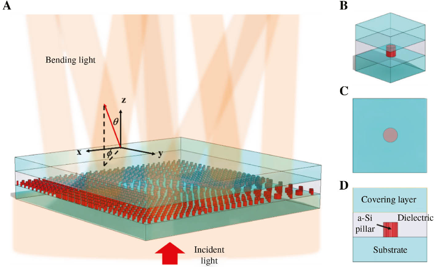
Schematic of the large-area pixelated metasurface beam deflector to generate random points.
(A) Schematic of the pixelated metasurface beam deflector (drawing not to scale), demonstrating the concept for random point generator. (B) The perspective view, (C) top view and (D) side view of a one unit cell of the a-Si nanopillar.
The beam deflector shapes the wavefront of the transmitted light with a phase gradient and deflects the light with a deflection angle θ, which is governed by the generalized Snell’s law [30], as presented in the following equation:
where the incident angle θi=0o (normal incidence), and hence the deflection angle, also known as bending angle θ, is determined by the phase gradient dφ/dx. The nanopillar pattern is oriented in a designed angle ϕ to determine the orientation angle of the bending direction. The orientation angle ϕ covers from 0° to 360°. The combination of the bending angle θ and the orientation angle ϕ enables the generation of two-dimensional (2D) point array.
To realize the phase gradient of the beam deflector, we use a supercell containing a number of nanopillars, whose diameter is chosen to provide the accumulated phase difference from one neighboring nanopillar to the other, resulting in a full 2π phase difference accumulation over the period of the supercell. According to Equation (1), the bending angle is determined by the period of the supercell. Figure 2A shows the simulation results of the phase shift and transmission for nanopillars with a variation of diameters, which is calculated by three-dimensional finite difference time domain (FDTD) method (FDTD Solutions, Lumerical Inc., Vancouver, British Columbia, Canada). In the simulation, the unit cell dimension is fixed at 545 nm, and the height of the nanopillar is 145 nm, with working wavelength at 940 nm. The phase shift and the transmission with respect to the diameter of the nanopillar is calculated for each metasurface unit cell. The range of the pillar diameters is chosen to be 221 to 396 nm, in order to cover the full range of phase shift (from 0 up to 2π) while maintaining a relatively high transmission (>70%).
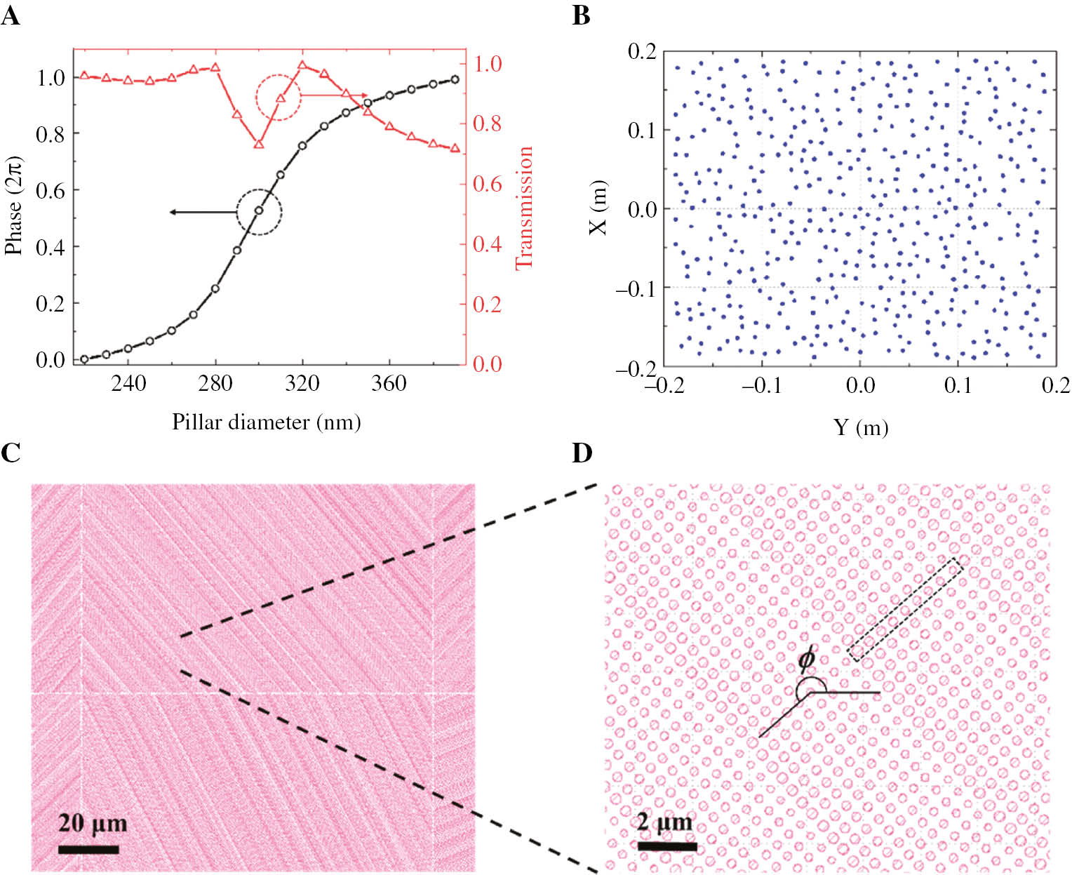
Design of the large-area pixelated metasurface beam deflector.
(A) Simulation of phase shift and transmission of building block for beam deflector (a-Si nanopillar with a unit cell of 545 nm and height of 145 nm embedded in dielectric media) as a function of diameter. (B) Designed 441 random point positions (relating to the bending angles θ and the orientation angles ϕ) on a screen with distance of 1 m away from the pixelated metasurface beam deflector. (C) Layout mask for the designed metasurface, showing pixel boundaries. (D) Zoomed-in view of (C), showing a supercell of beam deflector (denoted by a dotted rectangle) and nanopillar array with a designed orientation.
The design is able to achieve different bending and orientation angles for the transmitted light from each beam deflector to form a 2D point array. The 2D point array is designed within a square area with a diagonal length of 0.53 m on the surface located 1 m behind the metasurface, with the largest bending angle of 15°. The location of each point within the area is randomly generated, with the limitation on the minimum distance between two points of 1.8 cm. The metasurface pixel is 21×21, which gives 441 random points on the screen. The designed 2D point array is shown in Figure 2B. The layout of the pixelated metasurface beam deflector is partly shown in Figure 2C, and the zoomed-in view of one beam deflector is shown in Figure 2D. It is clear to see that the nanopillars with various diameters are arranged in one supercell denoted by the dotted rectangle, and the supercell has an orientation angle of ϕ.
3 Results and discussion
Figure 3A shows the fabricated 12-inch glass wafer, with its central die highlighted in a red dotted line. A zoomed-in view of the central die is illustrated in Figure 3B, with the pixelated metasurface beam deflector device highlighted. The CMOS-compatible fabrication process flow of the metasurface on glass wafer is shown in Figure 3C. It starts with a 12-inch (300-mm) silicon wafer, and a 1-μm thick SiO2 layer is deposited at the top via plasma enhanced chemical vapor deposition (PECVD). This SiO2 layer serves two purposes: it acts as an etch stop layer for the later process and a protective cladding layer at the top of the metasurface structure. The 100-nm-thick amorphous Si (a-Si) layer is deposited at the top via PECVD, as shown in step I. Next, a layer of photoresist is patterned at the top using a 193-nm ArF deep ultraviolet immersion lithography. The a-Si metasurface nanopillar structure is then formed by inductively coupled plasma (ICP) etching, as shown in step II. After the formation of the metasurface layer, a layer of transparent bonding glue is spin coated at the top of the a-Si layer, which is used to bond the silicon wafer with a standard 12-inch glass wafer, as shown in step III. The bonding glue is chosen based on its refractive index (n=1.479, k=0 at 940 nm), which is close to the glass substrate (n=1.452 at 940 nm) to make the a-Si nanopillar to be embedded in a more homogeneous environment [8]. Then the Si substrate thickness is reduced to about 20 μm through backside grinding and polishing process. In the last step, the remaining Si layer is removed completely by wet etching process, with the SiO2 layer as an etch stop, as shown in step IV. The metasurface layer under the scanning electron microscopy right after the ICP etching process is shown in Figure 3D. The projected view includes several pixels of beam deflector. Each pixel has a dimension of 120×120 μm and is designed to generate one spot by bending the input light beam to the designed direction. The enlarged view for one pixel is shown in Figure 3E. The nanopillars with various diameters are arranged and oriented with designed angles for light bending, which refers to Figure 2D. The shape of each nanopillar can be visualized in zoomed-in view in Figure 3F, showing a clear edge without defect after the patterning and etching process. The cross-section view of the nanopillar on the glass substrate is captured by transmission electron microscopy, as shown in Figure 3G. The shape of each pillar and the gap in between can be seen clearly. The height of the a-Si layer is measured to be 125 nm. These images prove the mass-manufacturing capability of the sub-wavelength metasurface structure using the immersion lithography technology for a 12-inch glass wafer.
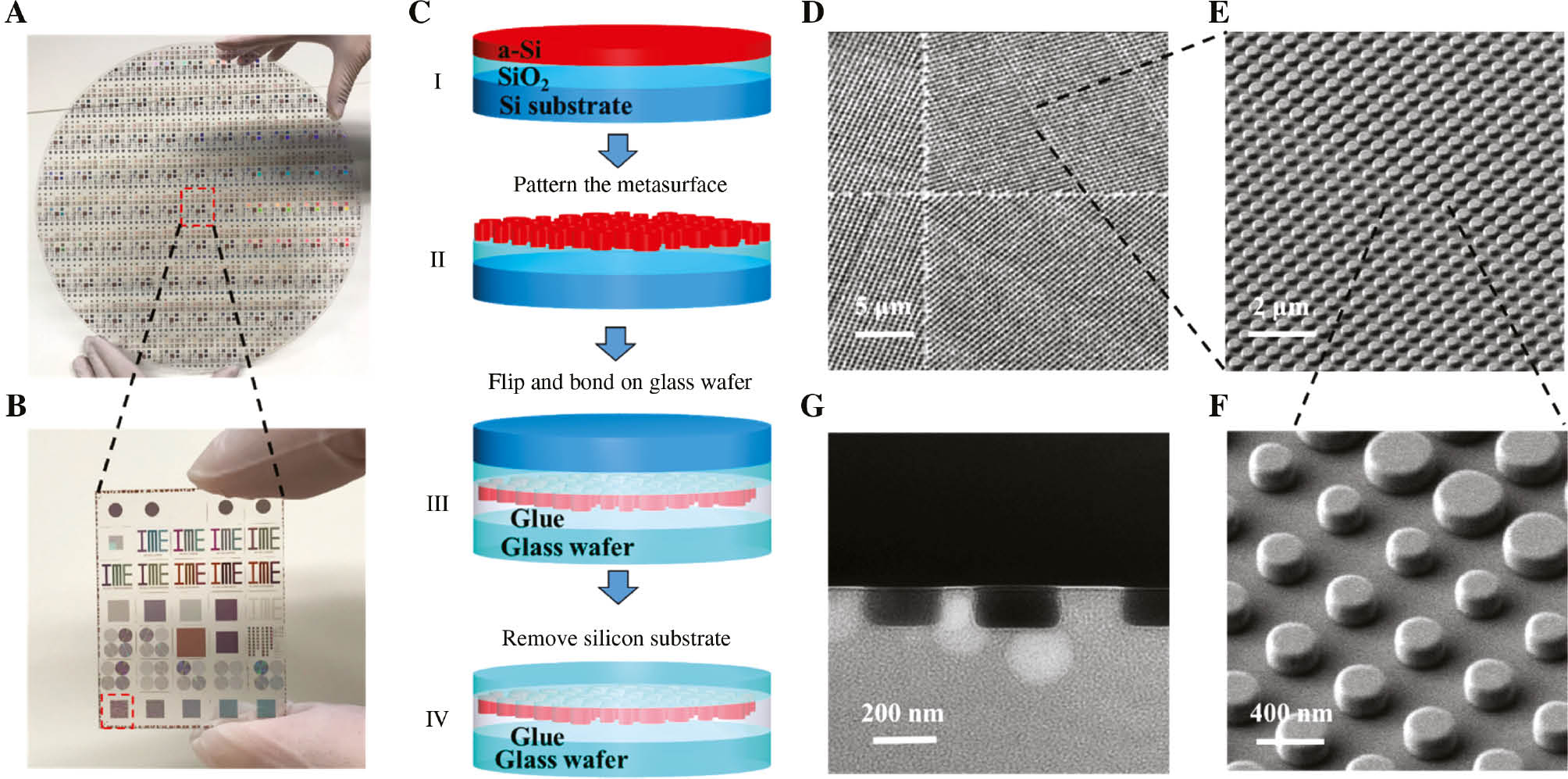
Fabrication of the large-area pixelated metasurface beam deflector on a 12-inch glass wafer.
(A) The photo of the fabricated 12-inch glass wafer, with highlighted area denoting central die. (B) Central die with dimension of 33×26 mm2, with highlighted area indicating the pixelated metasurface beam deflector. (C) Schematic of the fabrication process for layer transfer on glass wafer: (I) 12-inch Si wafer with SiO2 and a-Si layer deposited both via PECVD; (II) patterning of the photoresist using the 193-nm immersion lithography, followed by ICP etching of the metasurface layer; (III) spin coating of the bonding glue, followed by the bonding of Si wafer with glass wafer; and (IV) backside grinding and polishing, followed by wet etching process to remove the Si substrate. (D) The projected scanning electron microscopy of the fabricated metasurface layer after the ICP process, with projection angle of 45°. (E) Zoomed-in view of (D) for one pixel of beam deflector. (F) Zoomed-in view of (E) showing the nanopillar fabricated on Si substrate. (G) Cross-sectional transmission electron microscopy image of the nanopillars on glass embedded in bonding glue.
Figure 4A shows the characterization setup. A supercontinuum laser source (SuperK series, NKT Photonics Inc., Portland, OR, USA) cascaded with an acoustic optical tunable filter (AOTF) is used as a light source. A lens set, which is formed by two lenses with focus lengths of 6.24 and 20 mm, is used to expand the beam diameter to fully cover the metasurface area. A paper screen is placed at the back of the device with a distance of 31 cm. An infrared (IR) camera is used to capture the random points projected on the paper screen. The AOTF central wavelength is tuned to 940 nm. The image captured by the IR camera is presented in Figure 4B. The comparison between the designed 2D point array and the measurement result is made by taking the mirror image of the design and overlapping with the screen capture from experiment, as shown in Figure 4C. A good match can be observed. Note that the camera is placed on the side of the metasurface device with a viewing angle; hence, the width and the height of the design needs to be adjusted to compensate for the image distortion from the side view. In order to obtain the deflection efficiency of this random point generator, a hole with a diameter of 12 mm is drilled on the screen to pass the zeroth order diffraction. The area around the central hole looks more elongated along the vertical direction because the original beam from the supercontinuum cascaded by the AOTF source is elongated along the vertical direction. The optical power measured after the metasurface and after the screen through the hole are 0.43 and 0.23 mW, respectively. The deflection power efficiency can, therefore, be calculated by using 1 minus the ratio between 0.23 and 0.43, which gives 46.5%. Such efficiency can be further improved by optimizing the design of the nanopillars, taking the interactions among nearby pillars with various diameters into consideration. Furthermore, the efficiency performance of the device may also be affected by the critical dimension variation from the lithography process, which can be compensated by implementing the optical proximity correction technique. In addition, the transmission of the bonded glass wafer can be improved by optimizing the quality of the bonding process.
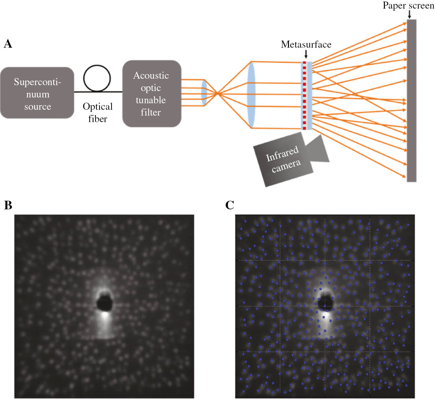
Characterization setup and results for the large-area pixelated metasurface beam deflector.
(A) Metasurface-based random point generator characterization setup, showing expanded input laser beam injected on the device and deflected to different directions on the screen behind the metasurface device. (B) The image on the screen captured by IR camera. (C) The comparison between the designed random point array with the experimental result, showing good match.
To conduct the spectral characterization of the metasurface, we vary the central wavelength of incident light from the AOTF, which is from 900 up to 980 nm, with a step of 20 nm. The deflection efficiencies at the wavelength of 900, 920, 940, 960 and 980 nm are measured to be 30.0%, 33.8%, 46.5%, 40.6% and 32.1%, respectively. The highest deflection efficiency is found to be at 940-nm wavelength, which matches with the designed wavelength of the device. A note worth to mention is that the images captured by the IR camera at different wavelengths are not comparable as the sensitivity of the IR camera detector varies with the wavelength.
The wafer-level uniformity of our platform was measured and analyzed in a previous work [24], which reports the amorphous silicon nanopillar with a comparable dimension as the ones used in this work. The wafer-level lithography shows good uniformity in terms of the range (max-min) and 3σ values. The maximum critical dimension variation was measured to be 7.65% after the etching process. Here, to verify the wafer-level uniformity on device performance, the optical deflection efficiency of the selected dies on the wafer are measured at 940 nm. The selected five dies are in the central row on the wafer and are indicated in Figure 5. The device is located at the left-bottom corner of each die and is highlighted in red. The deflection efficiencies on locations (0, −4), (0, −2), (0, 0), (0, 2) and (0, 4) are measured to be 40.4%, 43.5%, 46.5%, 45.7% and 44.7%, respectively. It can be found that the deflection efficiency has the highest value at the central die (0, 0) and becomes lower as the location of the die moves toward the edge of the wafer. The variation of deflection efficiency at different locations on the wafer should be contributed by the etching rate difference from the wafer center to the edge. Such variations can be further reduced by optimization of the etching process.
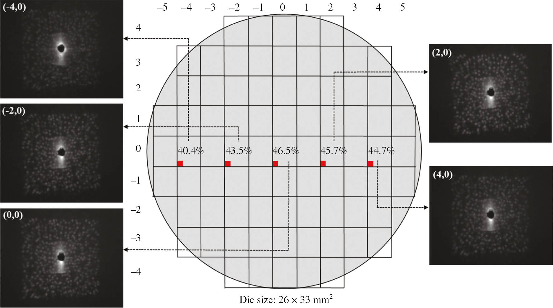
Wafer-level device performance uniformity measurement, showing the deflection efficiency measured in the central row.
At locations (0, −4), (0, −2), (0, 0), (0, 2) and (0, 4), the deflection efficiencies are measured to be 40.4%, 43.5%, 46.5%, 45.7% and 44.7%, respectively. The random points images captured by the IR camera show a slight difference in brightness contributed by the difference in deflection efficiency.
4 Conclusion
In summary, a large-area pixelated metasurface beam deflector based random point generator working at 940 nm is demonstrated. A CMOS-compatible fabrication process is developed to make the device on standard 12-inch glass wafer substrate. The random point generator contains a 21×21 array of beam deflector as pixels. Each pixel of beam deflector has a designed bending angle and orientation angle to control the propagation direction of the transmission beam. The random point array generated by the device is captured in experiment, showing good match with the original design. The potential applications of this device include sensing motion, facial recognition and light detection and ranging.
Acknowledgment
The authors would like to thank Dr. Ying Lin for assistance on photolithography. The appreciation extends to Dr. Vladimir Bliznetsov for assistance on wafer etching process and Dr. Stephanie Yang for the project initiation.
Funding: RIE2020 Advanced Manufacturing and Engineering (AME) Domain’s Core Funds: SERC Strategic Funds (A1818g0028).
References
[1] Sun S, Yang K-Y, Wang C-M, et al. High-efficiency broadband anomalous reflection by gradient meta-surface. Nano Lett 2012;12:6223–9.10.1021/nl3032668Search in Google Scholar PubMed
[2] Huang L, Chen X, Mühlenbernd H, et al. Dispersionless phase discontinuities for controlling light propagation. Nano Lett 2012;12:5750–5.10.1021/nl303031jSearch in Google Scholar PubMed
[3] Kita S, Takata K, Ono M, et al. Coherent control of high efficiency metasurface beam deflectors with a back partial reflector. APL Photonics 2017;2:046104.10.1063/1.4978662Search in Google Scholar
[4] Zhang Q, Li M, Liao T, Cui X. Design of beam deflector, splitters, wave plates and metalens using photonic elements with dielectric metasurface. Opt Commun 2018;411:93–100.10.1016/j.optcom.2017.11.011Search in Google Scholar
[5] Wang D, Fan Q, Wang J, Zhang Z, Liang Y, Xu T. All-dielectric metasurface beam deflector at the visible frequencies. Opto-Electron Rev 2017;44:103–7.Search in Google Scholar
[6] Emani NK, Khaidarov E, Paniagua-Domínguez R, et al. High-efficiency and low-loss gallium nitride dielectric metasurfaces for nanophotonics at visible wavelengths. Appl Phys Lett 2017;111:221101.10.1063/1.5007007Search in Google Scholar
[7] Zhou Z, Li J, Su R, et al. Efficient silicon metasurfaces for visible light. ACS Photonics 2017;4:544–51.10.1021/acsphotonics.6b00740Search in Google Scholar
[8] Yu YF, Zhu AY, Paniagua-Domínguez R, Fu YH, Luk’yanchuk B, Kuznetsov AI. High-transmission dielectric metasurface with 2π phase control at visible wavelengths. Laser Photonics Rev 2015;9:412–8.10.1002/lpor.201500041Search in Google Scholar
[9] Tittl A, Leitis A, Liu M, et al. Imaging-based molecular barcoding with pixelated dielectric metasurfaces. Science 2018;360:1105.10.1126/science.aas9768Search in Google Scholar PubMed
[10] Park Y, Kim J, Cho K-S, et al. Metasurface electrode light emitting diodes with planar light control. Sci Rep 2017;7:14753.10.1038/s41598-017-15254-3Search in Google Scholar PubMed PubMed Central
[11] Brière G, Ni P, Héron S, et al. An etching-free approach toward large-scale light-emitting metasurfaces. Adv Opt Mater 2019;7:1801271.10.1002/adom.201801271Search in Google Scholar
[12] Checcucci S, Bottein T, Gurioli M, Favre L, Grosso D, Abbarchi M. Multifunctional metasurfaces based on direct nanoimprint of titania sol-gel coatings. Adv Opt Mater 2019;7:1801406.10.1002/adom.201801406Search in Google Scholar
[13] Lee G-Y, Hong J-Y, Hwang S, et al. Metasurface eyepiece for augmented reality. Nat Commun 2018;9:4562.10.1038/s41467-018-07011-5Search in Google Scholar PubMed PubMed Central
[14] Li N, Su Z, Purnawirman, et al. Athermal synchronization of laser source with WDM filter in a silicon photonics platform. Appl Phys Lett 2017;110:211105.10.1063/1.4984022Search in Google Scholar PubMed PubMed Central
[15] Purnawirman, Li N, Magden ES, et al. Wavelength division multiplexed light source monolithically integrated on a silicon photonics platform. Opt Lett 2017;42:1772–5.10.1364/OL.42.001772Search in Google Scholar PubMed
[16] Magden ES, Li N, Raval M, et al. Transmissive silicon photonic dichroic filters with spectrally selective waveguides. Nat Commun 2018;9:3009.10.1038/s41467-018-05287-1Search in Google Scholar PubMed PubMed Central
[17] Singh N, Xin M, Vermeulen D, et al. Octave-spanning coherent supercontinuum generation in silicon on insulator from 1.06 μm to beyond 2.4 μm. Light Sci Appl 2018;7:17131.10.1038/lsa.2017.131Search in Google Scholar PubMed PubMed Central
[18] Su Z, Li N, Frankis HC, et al. High-Q-factor Al2O3 micro-trench cavities integrated with silicon nitride waveguides on silicon. Opt Express 2018;26:11161–70.10.1364/OE.26.011161Search in Google Scholar PubMed
[19] Li N, Vermeulen D, Su Z, et al. Monolithically integrated erbium-doped tunable laser on a CMOS-compatible silicon photonics platform. Opt Express 2018;26:16200–11.10.1364/OE.26.016200Search in Google Scholar PubMed
[20] She A, Zhang S, Shian S, Clarke DR, Capasso F. Large area metalenses: design, characterization, and mass manufacturing. Opt Express 2018;26:1573–85.10.1364/OE.26.001573Search in Google Scholar PubMed
[21] Hu T, Zhong Q, Li N, et al. Demonstration of a-Si metalenses on a 12-inch glass wafer by CMOS-compatible technology. 2019;arXiv e-prints arXiv:1906.11764.Search in Google Scholar
[22] Xu Z, Dong Y, Fu YH, et al. Embedded dielectric metasurface based subtractive color filter on a 300 mm glass wafer. In Conference on lasers and electro-optics. OSA Technical Digest. Optical Society of America, 2019, p. STh1O.4.10.1364/CLEO_SI.2019.STh1O.4Search in Google Scholar
[23] Xu Z, Dong Y, Tseng C-K, et al. CMOS-compatible all-Si metasurface polarizing bandpass filters on 12-inch wafers. Opt Express 2019;27:26060–9.10.1364/OE.27.026060Search in Google Scholar PubMed
[24] Hu T, Tseng C-K, Fu YH, et al. Demonstration of color display metasurfaces via immersion lithography on a 12-inch silicon wafer. Opt Express 2018;26:19548–54.10.1364/OE.26.019548Search in Google Scholar PubMed
[25] Li Z, Dai Q, Mehmood MQ, et al. Full-space cloud of random points with a scrambling metasurface. Light Sci Appl 2018;7:63.10.1038/s41377-018-0064-3Search in Google Scholar PubMed PubMed Central
[26] Mertz C, Navarro-Serment LE, MacLachlan R, et al. Moving object detection with laser scanners. J Field Robot 2013;30:17–43.10.1002/rob.21430Search in Google Scholar
[27] Spreeuwers L. Fast and accurate 3D face recognition. Int J Comput Vision 2011;93:389–414.10.1007/s11263-011-0426-2Search in Google Scholar
[28] Li W, Guo Q, Jakubowski MK, Kelly M. A new method for segmenting individual trees from the lidar point cloud. Photogramm Eng R S 2012;78:75–84.10.14358/PERS.78.1.75Search in Google Scholar
[29] Sampath A, Shan J. Segmentation and reconstruction of polyhedral building roofs from aerial lidar point clouds. IEEE T Geosci Remote 2010;48:1554–67.10.1109/TGRS.2009.2030180Search in Google Scholar
[30] Yu N, Genevet P, Kats PA, et al. Light propagation with phase discontinuities: generalized laws of reflection and refraction. Science 2011;334:333.10.1126/science.1210713Search in Google Scholar PubMed
©2019 Yuan Hsing Fu et al., published by De Gruyter, Berlin/Boston
This work is licensed under the Creative Commons Attribution 4.0 Public License.
Articles in the same Issue
- Review Articles
- Optically accessible memristive devices
- Role of nanophotonics in the birth of seismic megastructures
- Perovskite nanocrystals for energy conversion and storage
- Coherent nonlinear optics of quantum emitters in nanophotonic waveguides
- Optical force microscopy: combining light with atomic force microscopy for nanomaterial identification
- Enhanced nanodrug delivery in tumors after near-infrared photoimmunotherapy
- Metal-induced energy transfer
- Progresses in the practical metasurface for holography and lens
- Research Articles
- In-situ electrospun aligned and maize-like AgNPs/PVA@Ag nanofibers for surface-enhanced Raman scattering on arbitrary surface
- Plasmonic near-field scanning nanoscope with a cross-polarization detection technique
- Tunable atom-trapping based on a plasmonic chiral metamaterial
- Rigorous coupled-wave analysis of absorption enhancement in vertically illuminated silicon photodiodes with photon-trapping hole arrays
- Expanded Jones complex space model to describe arbitrary higher-order spatial states in fiber
- Color generation from self-organized metalo-dielectric nanopillar arrays
- Tandem white organic light-emitting diodes stacked with two symmetrical emitting units simultaneously achieving superior efficiency/CRI/color stability
- Ag nanoparticle-enhanced alkyl radical generation in photopolymerization for holographic recording
- Gate-tunable metafilm absorber based on indium silicon oxide
- High-performance and compact broadband terahertz plasmonic waveguide intersection
- Plasmonic quantum effects on single-emitter strong coupling
- Strong coupling with directional absorption features of Ag@Au hollow nanoshell/J-aggregate heterostructures
- Letter
- Broad band infrared modulation using spintronic-plasmonic metasurfaces
- Large-area pixelated metasurface beam deflector on a 12-inch glass wafer for random point generation