Colour centre generation in diamond for quantum technologies
-
Jason M. Smith

 ,
Simon A. Meynell
,
Simon A. Meynell

Abstract
Effective methods to generate colour centres in diamond and other wide band-gap materials are essential to the realisation of solid state quantum technologies based on such systems. Such methods have been the subject of intensive research effort in recent years. In this review, we bring together the various techniques used in the generation and positioning of colour centres in diamond: ion implantation, delta-doping, electron irradiation, laser writing and thermal annealing. We assess the roles and merits of each of these techniques in the formation of colour centres for different quantum technologies and consider future combinations of the techniques to meet the requirements of the most demanding applications.
1 Introduction
Research activity focused on colour centres in wide band gap materials, such as the diamonds used in quantum technologies, has increased in recent years. In many ways, point defects in diamonds act as isolated atoms with coherent optical transitions, Zeeman sublevels and hyperfine structure that allow a plethora of functionalities from which quantum technologies can be realised. Ensembles of colour centres have the potential to perform many of the applications of quantum optics using atomic gases, such as optical quantum memory [1] and magnetometry [2], [3], whilst isolated colour centres provide an alternative to trapped atoms and ions for quantum simulators and computers [4], [5], [6], [7] along with other applications, such as nano-magnetometry [8] and nano-thermometry [9]. Some of these applications are beginning to gain commercial footing. One example is magnetometry using negatively charged nitrogen-vacancy colour centres (NV−), which is currently being developed for microscopy (www.qnami.ch;www.qzabre.com) as well as navigation and vehicle detection applications (https://www.lockheedmartin.com/en-us/news/features/2019-features/tech-thats-cool-as-dark-ice.html).
Here, we review the methods used to create colour centres in diamond materials as a step in device fabrication. Many of the technologically important colour centres are defect complexes comprising at least one impurity atom and at least one lattice vacancy, bound together in a thermodynamically stable configuration. As such, methods for their generation tend to involve three elements: the introduction of impurities, the introduction of lattice vacancies and an annealing process to allow defect migration and bound state formation. Figure 1 illustrates this process via the example of the nitrogen-vacancy (NV) defect.
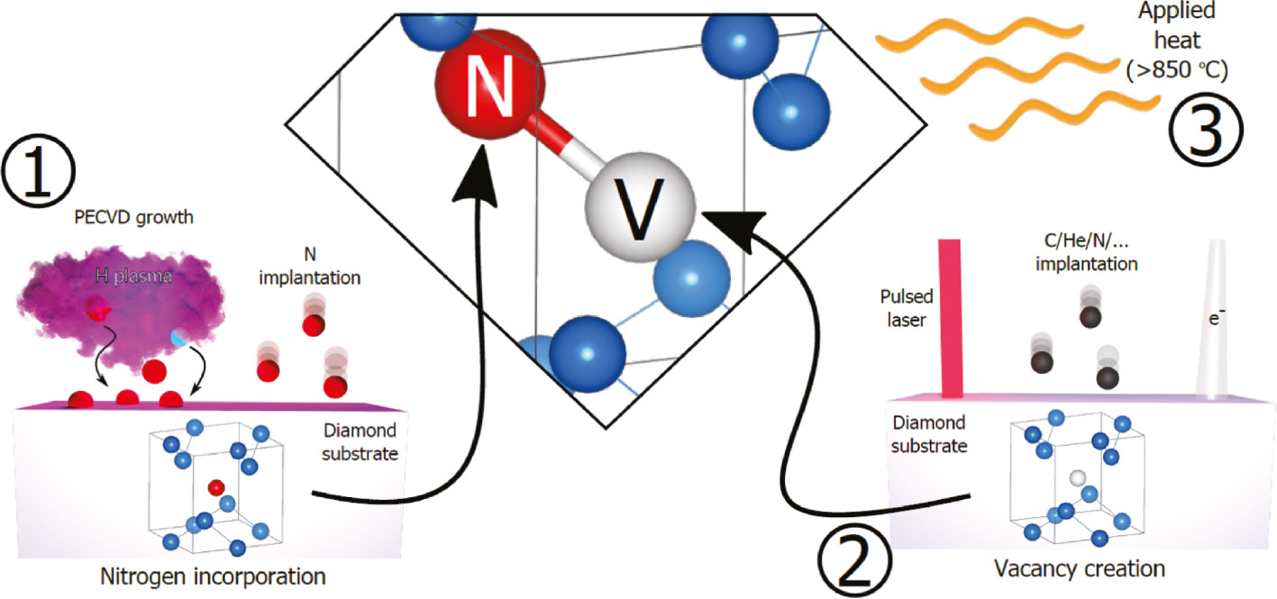
Processes involved in the generation of the nitrogen-vacancy colour centres in diamond.
We focus on the three main techniques for generating colour centres post-diamond growth, namely, ion irradiation/implantation, electron irradiation and laser processing, usually in combination with thermal annealing. Material growth and other elements of material processing are discussed only in the context of the material requirements for these colour centre fabrication methods. One exception is the delta doping of diamond, which can be beneficial in controlled depth positioning for colour centre generation and is thus covered in some detail. By bringing the various colour centre generation techniques together in a single review, we seek to compare their relative strengths in the context of the range of practical uses to which colour centres might be applied. We refer the reader to other recent reviews that discuss individual techniques for colour centre generation, including aspects of diamond growth [10] and microstructure fabrication [11], [12].
Before reviewing the fabrication techniques in detail, we first outline the principal requirements placed on the functional colour centres in diamond for different applications, which are key in setting the stage for the development of appropriate fabrication strategies. As will be seen, there are many considerations for specific applications, which may lead to a clear choice of colour centre and its generation method; however, it also often involves trade-offs between different parameters when no single fabrication technique can provide all the desired properties. We return to this topic in the discussion section after the process methods have been reviewed in detail. In discussing the applications, we do not seek to be comprehensive, rather we aim to highlight the principal fabrication challenges. Similarly, the references cited are intended to give examples that illustrate aspects of colour centre fabrication and so may not necessarily coincide with the state of the art in demonstrated functionality or performance.
We begin with applications involving ensembles of defects, where high concentrations are generally required as the device figure of merit scales with (typically the square root of) the number of colour centres present. For instance, in fluorescent labels for biosensing, where nanodiamonds are valued for their biological inertness and their stable, non-quenching fluorescence, it is desirable to achieve strong fluorescent signals from small nanodiamonds that cause minimal perturbation to biological function. NV centres are commonly used, created using electron irradiation or ion bombardment, followed by thermal annealing to create a high density of colour centres. Densities as high as 1/500 nm−3 are achieved, providing nearly 1000 NV centres in a 100 nm-diameter nanodiamond (http://www.fndbiotech.net/red_fluorescent_nds.html). High densities of NV centres are also needed for the hyperpolarisation of nuclear spins in contrast agents for medical MRI (https://www.nvision-imaging.com/).
Ensembles of NV centres are also widely developed for use in magnetometry, for which narrow spin transition linewidths in addition to high densities are important to provide high sensitivity. The requirement for narrow spin transition linewidth places an effective upper limit on the NV concentration based on the dominance of dipole-induced spin dephasing by either paramagnetic nitrogen or NV centres, depending on the N-NV conversion efficiency, at concentrations above 2 ppm. To reach this dipolar limit, other inhomogeneous broadening mechanisms, such as strain inhomogeneities, must be minimised and this requires that the NV creation processes should minimise defect densities that tend to create random local strain fields. Background fluorescence from other defects can limit the contrast of optically detected magnetic resonance and should also be minimised. Applications that require optical homogeneity in dense ensembles, such as optical quantum memories and diamond lasers, are still more demanding as optical transition energies are typically more sensitive to strain than are spin transitions. Exceptions to this rule occur for colour centres with similar electron distributions in the two states [13], which include the group IV vacancy defects SiV, GeV, SnV and PbV that show much lower inhomogeneous broadening in their optical transitions.
Finally, fabricating defects with preferred orientation can bring significant benefits to ensemble magnetometry because misaligned defects contribute unwanted background. Orientation alignment is one of the most challenging aspects of colour centre fabrication. Whilst the preferred orientation in an ensemble of colour centres has been achieved during growth [14], [15], this has yet to be achieved using post-growth processing techniques.
Many applications rely on the creation of colour centres with control over spatial localisation within the diamond. For example, the controlled depth positioning below a diamond surface is important for applications involving the use of colour centre ensembles for micrometre-scale spatial resolution imaging purposes [16], [17].
Spatial localisation becomes particularly important for applications involving individual colour centres, which often require alignment with sub-micrometre precision relative to other structures or components. Requirements vary from ~1 μm for alignment under a solid immersion lens (SIL) to ~10 nm for nano-probe tips, to a few nanometres for generating entangled spins [18]. In some cases, it may be beneficial to fabricate multiple colour centres within a small volume.
Some single-defect applications can be realised without careful positioning accuracy in defect fabrication, instead of aligning a structure to a single preselected defect. This approach is commonly taken with SILs [19] and with external Fabry Pérot microcavities [20] and are adequate for some applications, including single photon sources [21] and quantum repeaters [22]. With other devices, such as cantilever probe tips, a large number of structures can be fabricated and alignment can be achieved stochastically [23]. However, it seems likely that commercially attractive manufacturing routes will need to include sufficient positioning accuracy and colour centre yield so that the quasi-deterministic fabrication of useful devices can be achieved. The realisation of scalable devices containing multiple isolated defects aligned with optical or mechanical resonator structures, such as photonic crystals or external Fabry Pérot microcavity arrays, will require high positioning accuracy and high-yield colour centre fabrication (~50 nm in the case of photonics crystals and ~100 nm in the case of Fabry Pérots).
In addition to demanding high positioning accuracy and orientation alignment, the most advanced applications also demand long spin coherence, narrow and stable optical lines and good defect charge state stability, all of which are highly sensitive to the defect’s local environment. Therefore minimising damage to the lattice during defect creation and in post-processing annealing steps is a key consideration. Further advanced applications may also require the ability to engineer other parameters, such as the local distribution of nuclear spins for the creation of multi-qubit nodes for quantum computing [5], [6], [7]. For such devices, the ability not only to create but to controllably modify and delete individual colour centres may prove important. Such factors as compatibility with wafer-scale production and CMOS architectures will be important for realizing mass production in a commercial setting.
2 Ion implantation
Ion implantation is a well-known method that is widely used in the semiconductor industry and has found extensive use in colour centre generation [24]. It is the only method by which impurity atoms can be introduced into diamond post-growth; thus, it is a necessary step in the creation of colour centres for which a constituent impurity cannot readily be grown in to the diamond. It is also the only method to date by which the 3D positioning of impurities in diamond has been demonstrated.
Ion implantation has been used to create many different colour centres in diamond, including (but not limited to) NV, SiV, GeV, SnV and PbV, which have potential for quantum technologies either well-known or predicted [25]. However, the “ideal” colour centre for the most demanding applications has yet to be identified so there remains a continued interest in identifying new candidates. In 2018, Lühmann et al. reported a method for screening potential candidate colour centres by the implantation of oxygen, calcium, magnesium, fluorine and phosphorus followed by thermal annealing [26]. Such combinatorial efforts reflect the significant difficulty that remains in predicting both stable defect structures and their physical properties. Ion implantation is not limited to single species, and the implantation of molecular species, such as CN and N2, have been carried out in order to position the constituent ions within a few nanometres of each other in the diamond lattice [27].
2.1 Positioning of impurities using ion implantation
Implanting ions at defined positions is achieved by masking or focusing an ion beam, combined with a choice of kinetic energy to determine the implantation depth. The lateral and depth resolution of the implantation process is then determined by a combination of the kinetic energy and the properties of the target material [28].
The kinetic energy of the implanted ion will be dissipated by collisions with the electrons and the atomic nuclei. In particular, the collisions with nuclei lead to a strong deviation from the original direction wherein the higher the kinetic energy of the ions the greater the expected statistical deviation. This effect is called “straggling” and is very well studied. Figure 2 shows the penetration depth and the expected statistical deviation from the targeted position using the example of nitrogen and hydrogen ions in diamond. In order to achieve a deviation of less than 5 nm, for example, the ion energy must be limited to below 10 keV. The penetration depth in this case is about 10 nm. In general, a high lateral resolution can only be achieved for small kinetic energies and limits the penetration depth to a few nanometres. The creation of shallow implanted ions can then be achieved using contact masks – a standard method within semiconductor technology. Figure 3 shows the production of regular structures using contact PMMA masks on diamond. In this case, the number of colour centres generated is defined by Poisson statistics. However, contact masks are difficult for certain applications, such as the production of photonic crystals or implantation on diamond tips [29].
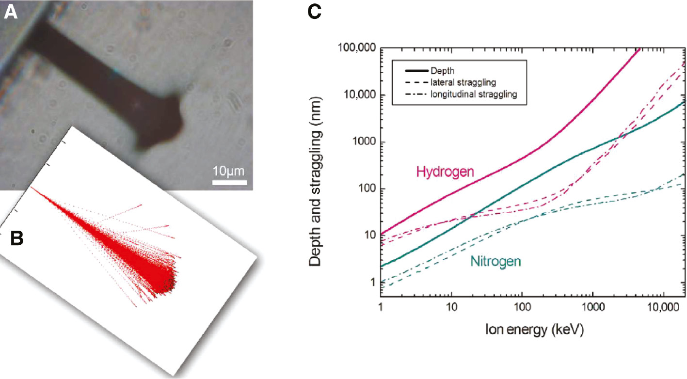
Penetration depth and the expected statistical deviation from the targeted position using the example of nitrogen and hydrogen ions in diamond.
(A) Optical image (side view) of a diamond sample implanted with a 3 MeV focused proton beam at high fluence. (B) SRIM simulation of 3 MeV protons implanted in diamond. (C) Plot of the ion range and straggle (lateral and longitudinal) simulated with SRIM for hydrogen and nitrogen implanted into diamond. Reproduced with permission from Sébastien Pezzagna and Jan Meijer, High-Resolution Ion Implantation from keV to MeV, INTECH: (2012).
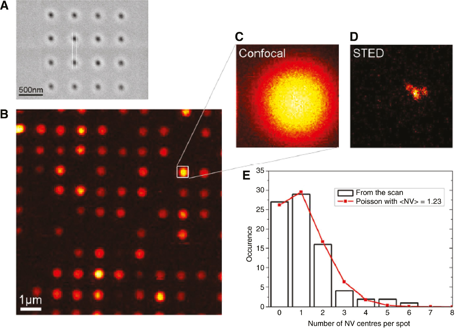
Production of regular structures using PMMA masks in diamond.
(A) SEM image of a PMMA photoresist mask patterned by electron beam lithography. The estimated hole diameter is 65 nm and the resist thickness is 230 nm. (B) Confocal fluorescence image of the surface of a diamond implanted with 55 keV CN-molecules through a PMMA mask. (C) Zoom on the inset in (B). (D) STED image of the same confocal spot, the single NV centres can be resolved. (E) Distribution of the number of NV centres per spot, fitted by a Poisson distribution with an average value of 1.23. Reproduced with permission from Sébastien Pezzagna and Jan Meijer, High-Resolution Ion Implantation from keV to MeV, INTECH: (2012).
An alternative method is the use of a hollow atomic force microscope (AFM) tip as a mask to achieve a high lateral resolution placement of shallow implanted ions [30]. In the first step, the AFM will be used to investigate the topographical structure of the surface, which allows an alignment within a few nanometres. In the second step, a nano-hole is fabricated in the AFM tip using a focused ion beam, as shown in Figure 4. The AFM tip with nano-hole then serves as a mask for ion implantation. The method allows a resolution of approximately 5–15 nm. An example of a spot containing about 8 NV centres is shown in Figure 5 and a schematic of the full implantation apparatus is shown in Figure 6.
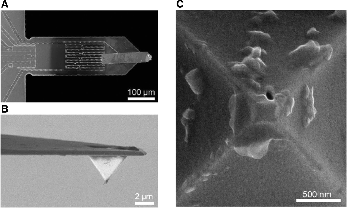
A nano-hole is fabricated in the AFM tip using a focused ion beam.
(A) SEM image of the piezo-resistive cantilever at the end of which the tip is glued. (B) SEM image of the hollow pyramidal AFM tip. (C) SEM image of the summit of the tip where a nano-hole has been drilled by focused ion beam milling. Reproduced with permission from Sébastien Pezzagna and Jan Meijer, High-Resolution Ion Implantation from keV to MeV, INTECH: (2012).
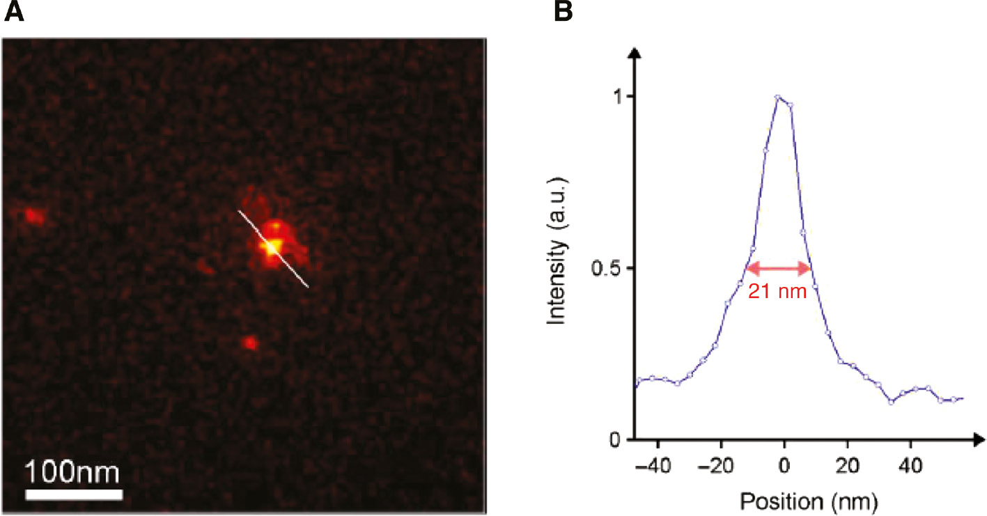
Spot containing about 8 NV centres.
(A) STED microscopy scan of the spot of NV centres created by implantation of 5 keV nitrogen ions through a reduced nano-hole. (B) Intensity profile corresponding to the line seen in (A). The optical resolution of the STED microscope is 10 nm. Reproduced with permission from Sébastien Pezzagna and Jan Meijer, High-Resolution Ion Implantation from keV to MeV, INTECH: (2012).
2.2 Deterministic control over number of implanted ions
The stochastic nature of ion implantation leads to a Poissonian statistical distribution of the number of implanted ions per site and represents a major hurdle for engineered devices in which a well-defined number of colour centres per site is likely to be necessary. For example, if a single colour centre is desired, the optimum result is obtained by setting the ion beam fluence such that, on average, only a single ion is implanted per given time interval. This method results in a probability of 37% to implant a single atom. This low probability of success makes the fabrication of complex devices impractical. For example, the production of a perfect array of only 10 qubits 1/(0.37)10 requires 20,800 attempts.
The deterministic implantation of single ions offers a potential way out and can be achieved by detecting the ion either pre- or post-impact with the substrate. The first method by which this was implemented was by detecting secondary electrons emitted from the substrate upon impact [31]. A second method to be developed, suitable for detection of ions of lower kinetic energy, was by the detection of excited electron-hole pairs [32]. The disadvantage of this latter method is that the device needs a diode structure to separate and detect the holes and electrons. In pre-impact detection, the ion will be detected before it reaches the material and is only directed to the target if it has been clearly identified beforehand. This method has the advantage of not generating false positive signals. Such methods have been realised at the groups of Prof. Schmidt-Kaler in Mainz who used ion trap detection [33], and in Leipzig using mirror charge detection [34]. In the ion trap scheme, individual ions are trapped, cooled and specifically accelerated to the target. As the ions have been identified in the trap, this method leads to an extremely reliable signal, resulting in a deterministic implantation with almost 100% probability of detection. A disadvantage is the high technical effort and the low implantation rate, because every ion has to be trapped and laser cooled. The mirror charge method uses a large number of rings in which a signal is generated when a charged particle passes through. When the signal exceeds a predetermined threshold, a fast beam shutter is activated such that only one ion is implanted in the target. This method is very fast, but it has high technical demands in terms of signal processing. Figure 7 shows a sketch of the image charge detection system at the Leipzig deterministic implantation group. The system is equipped with an EBIT (Electron beam ion Trap) source to provide highly charged ions and enhance the detection signal.
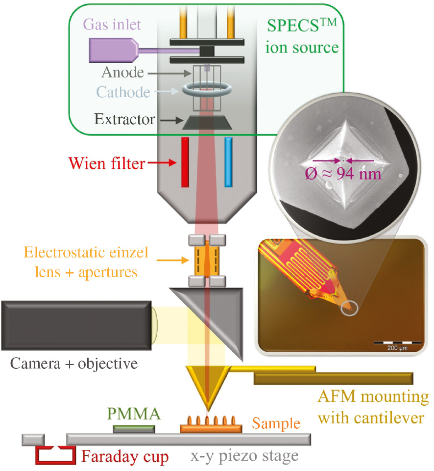
Nano-beam with AFM setup: ions are generated by SPECSTM ion source and separated by a Wien filter before entering an electrostatic einzel lens.
The ion beam crosses a mirror block that enables the observation of a pierced AFM tip, which is mounted on a cantilever. By using this technique, approaching single photonic structures and implanting through the bore in the tip allows spatial selective ion implantation of a few nm resolution. Reproduced with permission from T. Herzig et al. IEEE 2019, DOI: 10.1109/IIT.2018.8807909.
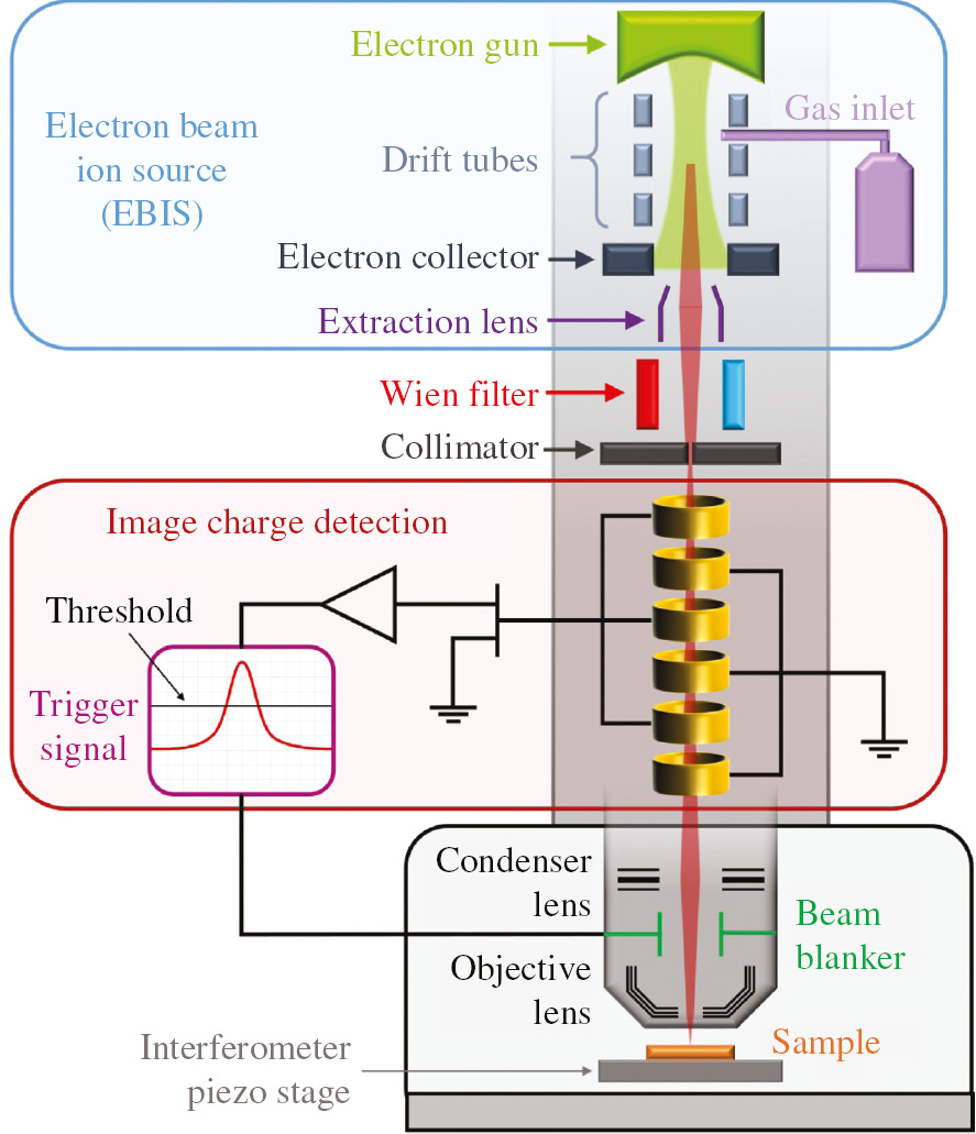
Concept for deterministic ion implantation: ions, coming from an EBIS, are separated by a Wien filter and collimator, before entering the image charge detector.
The image charge signals, induced into the detection tubes, are amplified and measured, thus allowing the distinction of single ions. The connected beam blanker is controlled by the trigger signal allowing deflection of ions with unknown or unwanted properties, thus ensuring deterministic implantation of defined single ions. Reproduced with permission from T. Herzig et al. IEEE 2019, DOI: 10.1109/IIT.2018.8807909.
Unfortunately, ion implantation has always been linked to the generation of additional defects. This fact emphasises the importance of understanding and manipulating defect generation in order to generate specific colour centres with a probability close to unity, thus minimising “collateral damage”. Highly coherent spin transitions and optical transitions have been reported from NV colour centres resulting from processes involving nitrogen implantation [35]. However, a recent report suggests that such optical transitions are not readily observed from NV centres, which include the implanted nitrogen atoms, rather by implantation-generated vacancies binding to nitrogen impurities that are already present in the lattice [36].
3 Combining nitrogen delta doping with ex-situ vacancy creation
3.1 Nitrogen doping during CVD growth
Doping during the plasma-enhanced chemical vapour deposition (PE-CVD) growth of diamond is another promising, though less explored, route towards creating colour centres in diamond. This bottom-up technique features gentle dopant incorporation with minimal lattice damage as well as highly controlled depth localisation; it has been successfully employed in creating highly coherent NV centres in diamond when combined with subsequent gentle vacancy creation methods, such as electron irradiation or remote ion implantation [37], [38].
Chemical vapour deposition is a highly non-equilibrium approach to diamond growth, carried out under conditions in which the equilibrium phase of carbon is graphite. A mixture of CH4 and H2 is introduced into a growth chamber and, upon the application of radio-frequency microwaves, ionises into a plasma. The role of the atomic hydrogen plasma is to create reactive hydrocarbons and radical sites upon which these hydrocarbons can incorporate into the diamond [39]. The atomic hydrogen will also preferentially etch away undesired diamond orientations or hydrocarbon species [40]. The growth itself consists of a series of reactions both at the surface and in the plasma above and will be sensitive to the injection position and flow rates of the gas [41] temperature and microwave power [42]. The technique of generating depth-localised, shallow NV centres in diamond via nitrogen depth-localised doping in 100-substrates during CVD growth was first developed in 2012 [37], [38].
The depth-localised doping technique developed by Ohno et al. consists of injecting nitrogen gas for a brief time (10 min) into the growth chamber while growing at a relatively slow rate (8 nm/h), with a thickness tuneable down to a few nanometres enabled by the slow growth rate. The (100)-oriented substrates are the most commonly used substrates for growth, though growth on other orientations has been demonstrated [43], [44], [45]. Following the introduction of nitrogen into the lattice, the NV centres are activated by a separate step using techniques such as electron irradiation [37], [46], carbon implantation [47], helium implantation [48] or laser writing [49] ex-situ. These vacancy-generation techniques will be discussed in Section 3.2 and Section 4.
The growth of thin homoepitaxial layers of engineered diamond enables the formation of high-quality, shallow NV centres, which are particularly useful for high spatial resolution sensing and imaging as well as for coupling to other quantum elements. In a typical growth, a homoepitaxial trilayer, consisting of a buffer layer, a doped layer and a capping layer, is grown atop a bulk, single-crystal diamond substrate, as shown in Figure 8A. The buffer layer serves to shield the NV centres from the sources of noise in the seed substrate and the capping layer protects against decoherence from the surface [50], [51]. These layers can be grown with 12C isotopically purified methane to reduce the decohering effects of the 13C nuclear spins. Control over the thickness and density of the nitrogen layer is governed by the time the nitrogen gas is on and by the flow rate of the gas. Slow growth rates help to minimise defects and strain to ensure NV centres with long coherence times.
![Figure 8: (A) Schematic of a typical homoepitaxial trilayer grown with PE-CVD. A buffer layer is grown atop the diamond substrate to protect from decoherence induced by impurities in the seed substrate, then a second layer is gently doped with nitrogen and finally a capping layer is grown to separate the doped layer from surface decoherence. (B) Carbon-13 concentration in a trilayer as measured by SIMS. Reproduced from Ref. [39], with the permission of AIP Publishing. For this growth, the buffer and capping layer are carbon-13 enriched whereas the doped layer is depleted. (C) A typical T2 coherence time in a grown NV as measured with a Hahn echo from Ref [46] in a 13C depleted grown layer. Reprinted with permission from Ref. [48]. Copyright 2016 American Chemical Society.](/document/doi/10.1515/nanoph-2019-0196/asset/graphic/j_nanoph-2019-0196_fig_008.jpg)
(A) Schematic of a typical homoepitaxial trilayer grown with PE-CVD. A buffer layer is grown atop the diamond substrate to protect from decoherence induced by impurities in the seed substrate, then a second layer is gently doped with nitrogen and finally a capping layer is grown to separate the doped layer from surface decoherence. (B) Carbon-13 concentration in a trilayer as measured by SIMS. Reproduced from Ref. [39], with the permission of AIP Publishing. For this growth, the buffer and capping layer are carbon-13 enriched whereas the doped layer is depleted. (C) A typical T2 coherence time in a grown NV as measured with a Hahn echo from Ref [46] in a 13C depleted grown layer. Reprinted with permission from Ref. [48]. Copyright 2016 American Chemical Society.
Figure 8B shows a secondary ion mass spectrometry (SIMS) measurement of a tri-layer with two 13C enriched layers surrounding a nitrogen-doped 13C depleted layer. Using this particular trilayer, Ohno et al. confirmed the nanometre-scale confinement of the central NV- rich layer by measuring the coupling of NV centres to 13C atoms in the outer layers. Importantly, the T2 coherence times of NV centres produced via delta-doping are reproducibly long [46] as shown in Figure 8C. As can be seen, there is a typical 1 ms T2 coherence time in a Hahn echo measurement.
3.2 Vacancy creation and NV conversion
Once nitrogen has been gently incorporated into the diamond at a specific depth and density, a secondary step of introducing vacancies into the diamond is needed to create NV centres. Various vacancy creation techniques are used to preserve the pristine CVD-grown diamond lattice and many of them feature additional advantages, such as lateral spatial localisation and tunable NV densities.
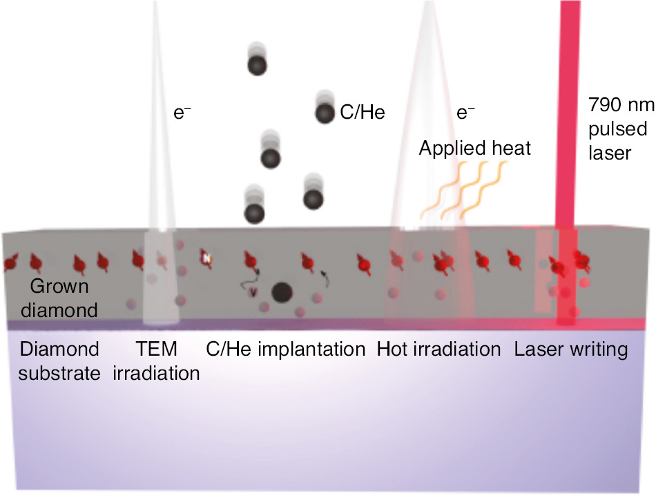
A variety of vacancy creation techniques are schematically depicted in Figure 9. A doped layer of nitrogen (represented by the red spins) is shown in a grown diamond. Progressing from left to right, focused electron irradiation from a transmission electron microscope (TEM) offers an energetically tunable way to write nanoscale patterns of vacancies into a diamond [46], [52]. Carbon [47] and helium [48] implantation are alternative methods for introducing vacancies in a controlled and gentle way in which ions can be implanted at a different depth than the nitrogen layer, thus minimising collateral damage at the nitrogen layer. An additional annealing step is then required for vacancy diffusion to form NV centres and to remove other residual defects, such as paramagnetic divacancies that may contribute additional sources of decoherence. Annealing is typically done in a separate step as discussed in Section 5, but a promising approach to further minimise collateral damage during vacancy formation involves annealing the sample with simultaneous irradiation [53] with the intent of minimising the formation of larger vacancy clusters and other vacancy-related defects before they have a chance to form. The high NV conversion rates have been achieved using this technique. Pulsed laser writing, another promising technique for both generating vacancies and in situ annealing, shall be discussed in Section 4.
A schematic depiction of various gentle vacancy creation techniques for CVD-doped nitrogen.
Left to right: low energy TEM irradiation is capable of gently generating localised vacancies. Ion implantation at a depth that is different from the nitrogen layer is another way of gently introducing vacancies. In this approach, a subsequent anneal will activate the NV centres as the vacancies diffuse to the nitrogen layer. Simultaneous annealing with vacancy creation is new technique whereby vacancies are introduced slowly during annealing. Laser writing vacancies is discussed in detail in Section 4 and is a promising technique for use in nitrogen-doped diamond.
3.2.1 Vacancy creation by electron irradiation
Electrons with sufficiently high energy can displace carbon atoms to form vacancies in the diamond lattice [54]. There are three primary ways in which an incident electron can dissipate energy within the diamond: Rutherford scattering, knock-on atoms and ionisation. The vacancy-creating damage of diamond from a Rutherford process is from scattering and subsequent displacement of a carbon atom, usually into an interstitial site. A minimum energy required to displace a carbon atom of about 30 eV [54] which translates to a minimum kinetic energy for electron irradiation of 145 keV [46]. Knock-on displacements occur when a displaced carbon causes further lattice damage, similar to that of implanted carbon ions. The third and final way by which electrons dissipate their energy is in the form of ionisation through the generation of electron-hole pairs in the diamond. The Monte Carlo simulation software called CASINO is used for calculating vacancy generation throughout an irradiated material [55].
MeV-scale electron irradiation is commonly used to form vacancies in nitrogen-rich diamond [2], [53], [56]. Growth, in conjunction with lower energy electron irradiation or other gentle vacancy creation techniques, is capable of creating ensembles of highly coherent NVs and has been shown to have sensitivities that are within a factor of 1.6 of the dipole-limit wherein the sensitivity is limited by the other NVs in the bath [52]. These dense and coherent spin ensembles are capable of high-sensitivity imaging on the mesoscale [46], [52] and could be useful in probing many-body spin physics in a highly controlled environment.
The precise control of the position of an NV centre in all three spatial dimensions can be achieved by using electron irradiation with a focused electron beam in a TEM incident on a delta-doped diamond sample, thus bringing the additional advantage of removing the need for masking. Recently, a TEM with energy tunable down to ~145 keV has been shown to produce reproducibly long coherence NV centres in the diamond lattice [46], [52]. Further, the small and controllable spot size of the TEM allows one to pattern arrays of varying dosages and sizes, and the depth extent of vacancy creation can be limited to ~1 μm in depth via control over the energy. Figure 10A shows a pattern produced by McLellan et al. [46]. In this paper, the T2’s of ~1 ms were reported to be combined with depth localisation to less than 4 nm via delta-doping and lateral localisation, and was limited by the vacancy diffusion length during annealing equal to or smaller than the optical diffraction limit. Going from left to right in Figure 10A, dosages of 1.6×10²², 2.5×10²⁰ and 2×10¹⁹ e/cm2 were used with a variable beam size in a 13C depleted layer. In this study, irradiation times varied from several minutes to hours. Typical dosages with conventional high energy (2 MeV) electron irradiation are of the order 1015–1017 e/cm2 [56]. The disparity between fluences illustrates one advantage of TEM irradiation: the tight focus of the beam allows for especially high fluence at the cost of the large areal coverage afforded to traditional high-energy electron irradiation techniques.
![Figure 10: (A) An array of NV centre ensembles created with TEM irradiation. The tunability of a TEM allows for a systematic varying of both dosage and energy. Reprinted with permission from Ref. [46]. Copyright 2016 American Chemical Society. (B) (i) An array of He implanted spots in a type 1b diamond. (ii) The optical properties of a He implanted diamond [48]. Reproduced from Ref. [48], with the permission of AIP Publishing. (C) Carbon implantation in a layer separated from a doped nitrogen layer. Reproduced from Ref. [47], with the permission of AIP Publishing.](/document/doi/10.1515/nanoph-2019-0196/asset/graphic/j_nanoph-2019-0196_fig_010.jpg)
(A) An array of NV centre ensembles created with TEM irradiation. The tunability of a TEM allows for a systematic varying of both dosage and energy. Reprinted with permission from Ref. [46]. Copyright 2016 American Chemical Society. (B) (i) An array of He implanted spots in a type 1b diamond. (ii) The optical properties of a He implanted diamond [48]. Reproduced from Ref. [48], with the permission of AIP Publishing. (C) Carbon implantation in a layer separated from a doped nitrogen layer. Reproduced from Ref. [47], with the permission of AIP Publishing.
3.2.2 Vacancy generation by ion implantation
Another way of gently introducing vacancies into the diamond is through controlled variants of ion implantation. Standard nitrogen implantation (Section 2) introduces vacancies as well as nitrogen, but can also introduce other defects (e.g. divacancies, vacancy clusters and inhomogeneous residual strain) that can act as sources of decoherence. To preserve the undamaged environment around a grown layer of nitrogen, one promising technique was developed by Huang et al. [48] where a scanning focused helium ion beam was used to pattern an array of vacancies while systematically varying the fluence. A helium ion beam can be focused down to 240 pm and can thus be used to produce highly laterally confined spots of vacancies. Figure 10B (i) from [48] shows one such array of implanted spots in a type 1b diamond wherein the ion dose varies between 108 and 1014 cm−2 with an energy of 30 keV. Figure 10B (ii) shows the resulting optical spectra. Another ion implantation technique shown to be useful in activating doped nitrogen layers was developed by Ohno et al. [47]. Here, 12C ions are implanted in a layer well-separated from the doped nitrogen in order to spatially separate the nitrogen layer from the damage layer. After annealing, the vacancies diffuse some distance away from the damaged implantation layer (depending on the annealing time) and then joined the doped nitrogen atoms to form NV centres. In this work, T2’s of over 300 μs are reported in 13C depleted CVD grown diamond, with NV density tunable with implanted 12C dose (Figure 10C).
4 Laser writing
Ultrafast laser processing has been used for decades to fabricate structures inside transparent materials from glasses, to polymers, crystals and biological materials. Some of the defects created are themselves colour centres [57]. However, it is only recently that it has been explored as a route to the controlled formation of defect complexes. A significant advantage of laser processing (using sub-band gap radiation) over other post-growth methods for materials engineering is that the nonlinearity of the interaction provides a route to localisation in three dimensions. In this section, we review recent developments in the use of ultrafast lasers for both the controlled creation of vacancies and local annealing of diamond.
4.1 Laser writing into bulk materials
In bulk crystalline materials, the generation of damage using sub-bandgap radiation is understood to occur via a sequential process involving first the generation of hot excitons, then subsequent relaxation delivering energy to the lattice [58]. The hot exciton generation process itself may involve three distinct light-induced processes: the generation of excitons via either multi-photon ionisation or Zener breakdown and the further heating of excitons via free-carrier absorption. The balance between MPI and the Zener breakdown is in close analogy with the ionisation of isolated atoms, as described by the Keldysh parameter [59]. In diamond, this parameter suggests that MPI will be the dominant process for photoionisation at optical intensities below about 25 W cm−2, whilst the Zener breakdown will dominate at higher intensities. A study involving theoretical analysis of photoionisation in bulk diamond using laser pulses at a wavelength of 800 nm concluded that carrier generation in the low pulse energy regime occurred via a 9-photon MPI process [60]. The need for hot excitons to create lattice damage may lead to significantly higher nonlinearities, which relate more directly the number of photons to the energy required for defect creation [61]. The subsequent relaxation and energy delivery generally involves some focusing process, either through the formation of polarons or via a lattice defect [58]. Photolytic defects, which are created via the non-radiative relaxation of electron-hole pairs, have been studied in dielectrics, such as alkali halides [62] and SiO2 [63].
To date, most of the works carried out on laser writing in diamond involved the graphitisation of regions in a bulk sample to fabricate electrically conductive wires for use in particle detectors [64], [65], [66] and optical waveguides [67], [68]. However, in some of these measurements, where samples were thermally annealed after laser processing, the creation of isolated NV centres near the graphitised region was observed as a result of the migration of vacancies from the damaged region to bind to nitrogen present in the diamond lattice. These reports provided the motivation for further work to attempt the controlled generation of single NV centres using laser processing. In 2017, Chen et al. demonstrated that single NV centres can be created effectively in diamond using the laser writing of vacancies followed by a thermal anneal [49]. In this work, single pulses of 300 fs duration at a wavelength of 790 nm with energies of 15–40 nJ were used to generate Frenkel defects, visible via GR1 (neutral vacancy) fluorescence, which then converted to NV centres upon thermal annealing. A single laser pulse at each site was used to avoid runaway damage to the lattice. Their results showed that a pulse energy regime existed in which sufficient vacancies can be generated to produce NV centres whilst allowing effective healing of the lattice during annealing. After annealing under nitrogen at 1000°C for 3 h, some of the NV centres created displayed lifetime-limited zero-phonon-line (ZPL) transitions at liquid helium temperatures (Figure 11) with transition energies that were robust to repumping of the NV− charge state. In a later work, it was shown that this method also achieved highly coherent electron spins, with Hahn echo measurements revealing T2 in the range 400–900 μs in diamond with natural abundance 13C [69]. The estimated positioning accuracy in the image plane of Frenkel defects was 100 nm, aided by the high nonlinearity of the interaction between the writing pulse and the diamond lattice and the use of spatial light modulator in the writing optics to correct for spherical aberration at the diamond surface. The resultant positional accuracy of the NV generation was measured to be about 200 nm in the image plane and estimated to be around 700 nm in depth, limited by the diffusion length of the vacancies during the anneal stage.
![Figure 11: Coherent optical transitions from single NV centres generated by laser writing of vacancies followed by a thermal anneal.(A) Fluorescence image of an array of processed sites showing laser-written NVs. (B) Example of a stable zero-phonon line (ZPL) transition with lifetime-limited linewidth. (C) Statistics from two samples (black and red) showing homogeneous and inhomogeneous line widths (sold and open circles, respectively) for different laser pulse energies. Originally published in Nature Photonics [49].](/document/doi/10.1515/nanoph-2019-0196/asset/graphic/j_nanoph-2019-0196_fig_011.jpg)
Coherent optical transitions from single NV centres generated by laser writing of vacancies followed by a thermal anneal.
(A) Fluorescence image of an array of processed sites showing laser-written NVs. (B) Example of a stable zero-phonon line (ZPL) transition with lifetime-limited linewidth. (C) Statistics from two samples (black and red) showing homogeneous and inhomogeneous line widths (sold and open circles, respectively) for different laser pulse energies. Originally published in Nature Photonics [49].
In a recent work [70], the process has been modified to include localised laser annealing accompanied by a fluorescence monitor to provide real-time feedback of colour centre creation. This method allows the near-deterministic creation of single NV centres (Figure 12A,B) and demonstrated improved positioning accuracy of around 35 nm in the image plane (Figure 12C) and 200 nm in depth (Figure 12D). The NV centres produced by this method showed shorter spin coherence times than those produced using thermal annealing. Narrow ZPL optical transitions have yet to be observed, although it should be noted that the diamond material used contained a relatively high nitrogen concentration of ~2 ppm and there is a significant potential for the further optimisation of the process.
![Figure 12: Writing of single NV centres using laser annealing.(A) A fluorescence monitor trace during the laser annealing process, showing NV-fluorescence appearing intermittently at first then as a stable signal. (B) A 5×5 array of processed sites in which a single NV centre has been created at 24 of the 25 sites. Measured scatter of NV centre positions (C) in the image plane and (D) in depth. Originally published in Optica [70].](/document/doi/10.1515/nanoph-2019-0196/asset/graphic/j_nanoph-2019-0196_fig_012.jpg)
Writing of single NV centres using laser annealing.
(A) A fluorescence monitor trace during the laser annealing process, showing NV-fluorescence appearing intermittently at first then as a stable signal. (B) A 5×5 array of processed sites in which a single NV centre has been created at 24 of the 25 sites. Measured scatter of NV centre positions (C) in the image plane and (D) in depth. Originally published in Optica [70].
The fluorescence monitor used in [70] provides some information regarding the dynamics of the NV centre formation process, with clear steps in fluorescence intensity observed showing single NV centre creation and destruction. The observations suggest that the annealing process mobilises both vacancies and interstitials, consistent with the low activation energies for the diffusion of these defects [71], [72].
A full theoretical model for the laser interaction with diamond has yet to be validated with experimental data. The high nonlinearities observed are beneficial in leading to high spatial resolution. However, these make the process challenging to control such that pulse energies are sufficient to anneal the diamond but without creating runaway damage. Kurita et al. have shown recently that the balance between colour centre generation and graphitisation depends on pulse duration [73], with 40 fs pulses providing a higher rate of NV centre generation relative to graphitisation than 1 ps pulses (Figure 13). This observation might suggest that the high exciton temperatures resulting from free carrier absorption serve to increase the degree of lattice damage.
![Figure 13: Dependence of laser-induced NV generation in bulk diamond on laser pulse duration.The images show fluorescence from arrays of processed sites with laser pulse durations of (A) 40 fs and (B) 1 ps. Pulse energies increase from the bottom rows to the upper rows in each image. Bright points indicate generation of NV centres whilst dark points are graphitised sites. Reproduced with permission from [73].](/document/doi/10.1515/nanoph-2019-0196/asset/graphic/j_nanoph-2019-0196_fig_013.jpg)
Dependence of laser-induced NV generation in bulk diamond on laser pulse duration.
The images show fluorescence from arrays of processed sites with laser pulse durations of (A) 40 fs and (B) 1 ps. Pulse energies increase from the bottom rows to the upper rows in each image. Bright points indicate generation of NV centres whilst dark points are graphitised sites. Reproduced with permission from [73].
4.2 Laser nano-ablation at the diamond surface and colour centre formation
The generation of near-surface NV centres by laser processing has been reported by two groups. In 2013 Liu et al. [74] reported the generation of ensembles and isolated NV centres after processing with 100 fs pulses of 800 nm light with energy of 4 μJ. The pulses were focused about 2 μm above the diamond surface, such that pulse intensities reached 3×10¹³ W cm−2 sufficient to ionise airborne nitrogen and irradiate the diamond surface with high energy electrons.
Kononenko et al. reported the generation of NV centres during nano-ablation of the diamond surface using a frequency tripled Ti:Sapphire laser (λ=266 nm) [75]. Based on the measured dependency of ablation rate and NV fluorescence intensity on the laser pulse fluence (Figure 14), they proposed a mechanism by which carbon-carbon bonds were broken via a two-photon process, such that ablation occurred via a photo-oxidation of the surface, scaling as the fourth power of the laser fluence, whilst NV formation included additional diffusion of vacancies from the surface to subsurface nitrogen, scaling as the sixth power of the fluence. NV centre generation followed a logarithmic dependence on the number of pulses.
![Figure 14: Dependence of nanoablation rate and photoluminescence signal from near-surface NV centres on laser fluence using 266 nm, 100 fs pulses.nc represents the nonlinearity to break a single C-C bond. Reproduced with permission from [75].](/document/doi/10.1515/nanoph-2019-0196/asset/graphic/j_nanoph-2019-0196_fig_014.jpg)
Dependence of nanoablation rate and photoluminescence signal from near-surface NV centres on laser fluence using 266 nm, 100 fs pulses.
nc represents the nonlinearity to break a single C-C bond. Reproduced with permission from [75].
In a later paper, the same group explored how the nano-ablation and NV generation dynamics varied with laser wavelength, using 266 nm, 400 nm and 800 nm [76]. Nano-ablation did not occur with 800 nm light, suggesting that the shorter wavelengths might be required to activate oxygen on the diamond surface and trigger the nano-ablation process. They also showed that the observed increase in PL intensity correlated closely with nano-ablation depth and followed the same roughly logarithmic dependence for 266 nm as for 400 nm light (Figure 15).
![Figure 15: Correlation between measured PL intensity of near-surface NV centres and depth of nanoablation crater, for processing wavelengths of 266 nm and 400 nm.Reproduced with permission from [76].](/document/doi/10.1515/nanoph-2019-0196/asset/graphic/j_nanoph-2019-0196_fig_015.jpg)
Correlation between measured PL intensity of near-surface NV centres and depth of nanoablation crater, for processing wavelengths of 266 nm and 400 nm.
Reproduced with permission from [76].
Laser writing has the potential for use in the creation of other colour centres in wide-gap materials and, recently, the generation of single VSi defects in Si-C has been reported [61]. In this work, a nonlinearity for the laser-generated vacancies was measured to be 15.5, consistent with a measured positioning accuracy of 80 nm, which was 3.7 times smaller than the diffraction-limited beam focus and with a displacement threshold energy for the Si atom in SiC of approximately 25 eV [77].
5 Thermal treatment
The creation of an NV centre requires the diffusion of a vacancy, either already present in the diamond or generated by one of the aforementioned methods, to a substitutional nitrogen atom. The annealing process used to facilitate this diffusion is also used to repair any additional defects created during impurity implantation or vacancy generation. It has been shown that annealing at 1200°C significantly increases the electron spin coherence time of NV centres generated by ion implantation [78]. The thermal treatment is, therefore, generally designed to achieve the highest possible conversion rate from substitutional nitrogen atoms into NV centres, whilst removing other paramagnetic defects that would induce decoherence [25], [26], [79]. The processes of defect diffusion and dissociation are all thermally activated, each with its own corresponding activation energy, whereby the annealing temperature determines which processes occur and at what rates. By the careful selection of the annealing time and temperature, the formation or removal of specific defects or colour centres can be encouraged or prevented.
The dynamics of the photoactive defect centres during the annealing procedure can be followed by photoluminescence (PL) and is shown in Figure 16 [26]: the neutral single vacancies (V0) are visible in the PL spectrum as GR1 centre at 740–800 nm, the characteristic ZPL is found at 741 nm [80]. The diffusion of vacancies starts at approx. 300–600°C [81] and the GR1 emission disappears [26]. At approximately 800°C the recombination of double C occurs, as evidenced by a decrease of 3H centre fluorescence at 503 nm [80]. At this temperature the activation energy to create the NV centres will be reached [26] and the creation of the NV centre starts. From about 1300°C in damaged diamond or 1600°C in undamaged diamond, the NV centres dissociate, whereas in diamonds with a high N or NV content H3 centres (N-V-N) are formed (Figure 16B) [26].
![Figure 16: The dynamics of the photoactive defect centres during the annealing procedure can be followed by photoluminescence.(A) Fluorescence intensity versus annealing temperature of different defects: NV, H3, GR1 and 3H. The NV centres correspond to implantations of N at 45 keV and ~1015 cm−2 (orange dots) and to 300 keV and ~1013 cm−2 (red dots) [26]. (B) Fluorescence intensity versus annealing temperature for the NV and H3 centres [26].](/document/doi/10.1515/nanoph-2019-0196/asset/graphic/j_nanoph-2019-0196_fig_016.jpg)
The dynamics of the photoactive defect centres during the annealing procedure can be followed by photoluminescence.
(A) Fluorescence intensity versus annealing temperature of different defects: NV, H3, GR1 and 3H. The NV centres correspond to implantations of N at 45 keV and ~1015 cm−2 (orange dots) and to 300 keV and ~1013 cm−2 (red dots) [26]. (B) Fluorescence intensity versus annealing temperature for the NV and H3 centres [26].
Another way to study the dynamics of defects of paramagnetic centres is to use electron paramagnetic resonance (EPR) measurements [82] which shows that the majority of paramagnetic defects disappear at approximately 1100°C [82]. Another parameter that determines the dynamics and concentration of defects is the location of the chemical potential during the annealing process [83]. For example, by determining the charge state of defects, such as holes, the formation of colour centres or defect clusters can be influenced positively or negatively. This also explains the low formation rate of NV centres on the surface of diamonds due to the band bending [79]. Thus, a high concentration of nitrogen could also influences the formation of defect clusters given that nitrogen acts as a donor. In addition, there is the influence of stress or surface defects, which can changed the diffusion of vacancies as a whole or in a certain direction [26]. Furthermore, the production of NV centres is influenced by the hydrogen content [26], [84]. Hydrogen can bind to the defects in the diamond and be incorporated during the growth process. This either favours or inhibits the diffusion properties and the formation of certain defect clusters. The content of hydrogen in the usual CVD growth process is only insufficiently known and can vary greatly [84]. Hydrogen can bind to NV centres to form NVH complexes. As this centre is stable up to temperatures of 1500 °C, its formation can unfortunately not be prevented or reversed by a high annealing temperature.
If one also considers that the combination of these complex processes is strongly dependent on the temperature and temperature progression during heating and cooling and that these are often not exactly determined, the partially very different results can be explained in the literature. Fortunately, the diffusion constant of nearly all other atoms, except vacancies and hydrogen, is extremely low in diamond, thus implanted atoms or colour centres stay at the place during the annealing procedure. It was already shown that even the direction of the NV centre is stable until 1100°C [26]. This makes the fabrication of very small structures like a quantum register based on single NV centres possible.
In summary, as many paramagnetic defects can be annealed at a temperature of 1100°C and the NV centre is stable until approximately 1300°C, an annealing temperature of 1100–1200°C can be described as optimal. If one wishes to maximise NV creation and lose as few point defects as possible before NV centres form, this temperature should be reached as quickly as possible.
Diamond oxidises at approximately 580°C, so the thermal treatment should take place in a vacuum or in an inert gas atmosphere. Overall, vacuum has proven to be advantageous because contamination with oxygen can hardly be prevented by multiple flushing. To avoid contamination, using a furnace made of high-purity graphite is an advantage. Metals, such as iron, lead to an etching process or to carbides and direct contact should be avoided in any case. A flashing with forming gas (90% N and 10% hydrogen) leads to a reduction of graphite on the surface, but hydrogen can dissociate at high temperatures and cause a reduction of the NV content at the surface.
6 Discussion and outlook
The preceding sections show that no single approach to defect fabrication fulfils all of the requirements for the range of potential applications. For the generation of ensembles of colour centres throughout the bulk only electron irradiation offers sufficient penetration depth to introduce vacancies uniformly through a sample, whilst also offering a relatively gentle and controllable method to produce high densities of coherent colour centres. For near-surface colour centres, both e-beam combined with delta doping and shallow ion implantation can be used. Ion implantation is an essential step to produce colour centres containing impurities that cannot be “grown in”.
Depth positioning and uniform ensembles at specified depth can be achieved using ion implantation of undoped material, as well as delta-doping of materials during growth which offers even tighter depth confinement. For the generation of colour centres at defined positions throughout the volume of a bulk diamond, the high nonlinearity of the laser writing technique provides a unique advantage.
All methods offer the possibility of creating single colour centres, but only laser writing has so far achieved this deterministically, as a result of local annealing combined with inline fluorescence feedback. The possibility of using this process to locally modify colour centres and their environments in a controllable way is tantalising but has yet to be demonstrated to a useful degree.
Long electron spin coherence times and coherent optical transitions have been achieved with all three methods, although the creation of local lattice damage around implanted ions raises a challenge in creating coherent optical transitions in non-centrosymmetric colour centres, such as the NV centre.
There are several ways in which these methods could be combined to achieve advanced colour centre engineering. For example, laser annealing and fluorescence feedback could be integrated with either ion implantation or e-beam irradiation to allow deterministic writing. A comprehensive method for defect engineering could involve all three processes: deterministic ion implantation to introduce the impurity atom, e-beam irradiation to generate vacancies nearby and a combination of thermal and laser annealing with feedback to form the colour centre complex. Integrating the three techniques into a single instrument may offer the ability to “repeat until success”, a great advantage given the unavoidably random nature of the defect environment.
The use of high temperature (>1200°C) thermal annealing is a promising way to remove lattice damage, such as divacancies and vacancy clusters created during ion implantation. The tendency of impurities (e.g. nitrogen) to migrate and form clusters under such high temperatures can potentially be mitigated by the charging of defects via doping.
Another open question is whether local annealing can be achieved near the diamond surface in such a way that coherent colour centres can be generated. The demonstrations of colour centre generation in the nano-ablation regime may provide a route going forward, and the use of heat absorber (e.g. graphite) on the surface for local annealing have also been suggested.
In summary, the generation of colour centres has advanced significantly in recent years, such that highly coherent colour centres can be produced on-demand with positioning accuracy of order 10 nm. The initial results showing the deterministic writing via local processing offer the beginnings of controlled device engineering for quantum technologies.
Acknowledgments
We acknowledge discussions with Dr. Claire McLellan.
References
[1] Poem E, Weinzetl C, Klatzow J, et al. Broadband noise-free optical quantum memory with neutral nitrogen-vacancy centres in diamond. Phys Rev B 2015;91:205108.10.1103/PhysRevB.91.205108Suche in Google Scholar
[2] Acosta VM, Bauch E, Ledbetter MP, et al. Diamonds with a high density of nitrogen-vacancy centres for magnetometry applications. Phys Rev B 2009;80:115202.10.1103/PhysRevB.80.115202Suche in Google Scholar
[3] Wolf T, Neumann P, Nakamura K, et al. Subpicotesla diamond magnetometry. Phys Rev X 2015;5:041001.10.1103/PhysRevX.5.041001Suche in Google Scholar
[4] Benjamin SC, Lovett BW, Smith JM. Prospects for measurement-based quantum computing using solid state spins. Laser Photonics Rev 2009;3:556.10.1002/lpor.200810051Suche in Google Scholar
[5] Nickerson NH, Fitzsimons JF, Benjamin SC. Freely scalable quantum technologies using cells of 5-to-50 qubits with very lossy and noisy photonic links. Phys Rev X 2014;4: 041041.10.1103/PhysRevX.4.041041Suche in Google Scholar
[6] Rong X, Geng J, Shi F, et al. Experimental fault-tolerant universal quantum gates with solid-state spins under ambient conditions. Nat Commun 2015;6:8748.10.1038/ncomms9748Suche in Google Scholar PubMed PubMed Central
[7] Bradley CE, Randall J, Abobeih MH, et al. A 10-qubit solid-state spin register with quantum memory up to one minute. Phys Rev X 2019;9:031045.10.1103/PhysRevX.9.031045Suche in Google Scholar
[8] Balasubramanian G, Chan IY, Kolesov R, et al. Nanoscale imaging magnetometry with diamond spins under ambient conditions. Nature 2008;455:648.10.1038/nature07278Suche in Google Scholar PubMed
[9] Kucsko G, Maurer PC, Yao NY, et al. Nanometre-scale thermometry in a living cell. Nature 2013;500:54.10.1038/nature12373Suche in Google Scholar PubMed PubMed Central
[10] Ekimov EA, Kondrin MV. Vacancy-impurity centres in diamond: prospects for synthesis and applications. Physics Uspekhi 2017;60:539.10.3367/UFNe.2016.11.037959Suche in Google Scholar
[11] Orwa JO, Greentree AD, Aharonovich I, et al. Fabrication of single optical centres in diamond – a review. J Luminescence 2010;130:1646.10.1016/j.jlumin.2009.12.028Suche in Google Scholar
[12] Kalish R. The role of ion-implantation in the realization of spintronic devices in diamond. Nucl Instrum Methods Phys Res B 2012;272:42.10.1016/j.nimb.2011.01.029Suche in Google Scholar
[13] Udvarhelyi P, Nagy R, Kaiser F, Lee S-Y, Wrachtrup J, Gali A. Spectrally stable defect qubits with no inversion symmetry for robust spin-to-photon interface. Phys Rev Appl 2019;11:044022.10.1103/PhysRevApplied.11.044022Suche in Google Scholar
[14] Michl J, Teraji T, Zaiser S, et al. Perfect alignment and preferential orientation of nitrogen-vacancy centres during chemical vapor deposition diamond growth on (111) surfaces. Appl Phys Lett 2014;104:102407.10.1063/1.4868128Suche in Google Scholar
[15] Lesik M, Tetienne J-P, Tallaire A, et al. Perfect preferential orientation of nitrogen-vacancy defects in a synthetic diamond sample. Appl Phys Lett 2014;104:113107.10.1063/1.4869103Suche in Google Scholar
[16] DeVience SJ, Pham LM, Lovchinsky I, et al. Nanoscale NMR spectroscopy and imaging of multiple nuclear species. Nat Nanotech 2015;10:129.10.1038/nnano.2014.313Suche in Google Scholar PubMed
[17] Tetienne J-P, Dontschuk N, Broadway DA, Stacey A, Simpson DA, Hollenberg LCL. Quantum imaging of current flow in graphene. Sci Adv 2017;3:1602429.10.1126/sciadv.1602429Suche in Google Scholar PubMed PubMed Central
[18] Dolde F, Jakobi I, Naydenov B, et al. Room-temperature entanglement between single defect spins in diamond. Nat Phys 2013;9:139.10.1038/nphys2545Suche in Google Scholar
[19] Marseglia L, Hadden JP, Stanley-Clarke AC, et al. Nanofabricated solid immersion lenses registered to single emitters in diamond. Appl Phys Lett 2011;98:133107.10.1063/1.3573870Suche in Google Scholar
[20] Johnson S, Dolan PR, Grange T, et al. Tunable cavity coupling of the zero phonon line of a nitrogen vacancy defect in diamond. New J Phys 2015;17:122003.10.1088/1367-2630/17/12/122003Suche in Google Scholar
[21] Dolan PR, Adekanye S, Trichet AAP, et al. Robust, tunable, and high purity triggered single photon source at room temperature using a nitrogen-vacancy defect in diamond in an open microcavity. Opt Express 2018;26:7056.10.1364/OE.26.007056Suche in Google Scholar PubMed
[22] Hensen B, Bernien H, Dréau AE, et al. Loophole-free Bell inequality violation using electron spins separated by 1.3 kilometres. Nature 2015;526:682.10.1038/nature15759Suche in Google Scholar PubMed
[23] Appel P, Neu E, Ganzhorn M, et al. Fabrication of all diamond scanning probes for nanoscale magnetometry. Rev Sci Inst 2016;87:063703.10.1063/1.4952953Suche in Google Scholar PubMed
[24] Meijer J, Burchard B, Domhan M, et al. Generation of single colour centres by focused nitrogen implantation. Appl Phys Lett 2005;87:261909.10.1063/1.2103389Suche in Google Scholar
[25] Pezzagna S, Rogalla D, Wildanger D, Meijer J, Zaitsev A. Creation and nature of optical centres in diamond for single-photon emission-overview and critical remarks. New J Phys 2011;13:035024.10.1088/1367-2630/13/3/035024Suche in Google Scholar
[26] Lühmann T, Raatz N, John R, et al. Screening and engineering of colour centres in diamond. J Phys D Appl Phys 2018;51:483002.10.1088/1361-6463/aadfabSuche in Google Scholar
[27] Spinicelli P, Dréau A, Rondin L, et al. Engineered arrays of nitrogen-vacancy colour centres in diamond based on implantation of CN- molecules through nanoapertures. New J Phys 2011;13:025014.10.1088/1367-2630/13/2/025014Suche in Google Scholar
[28] Loretz M, Pezzagna S, Meijer J, Degen CL. Nanoscale nuclear magnetic resonance with a 1.9-nm-deep nitrogen-vacancy sensor. Appl Phys Lett 2014;104:033102.10.1063/1.4862749Suche in Google Scholar
[29] Riedrich-Moller J, Pezzagna S, Meijer J, et al. Nanoimplantation and Purcell enhancement of single nitrogen-vacancy centres in photonic crystal cavities in diamond. Appl Phys Lett 2015;106:221103.10.1063/1.4922117Suche in Google Scholar
[30] Pezzagna S, Wildanger D, Mazarov P, et al. Nanoscale engineering and optical addressing of single spins in diamond. Small 2010;6:2117–21.10.1002/smll.201000902Suche in Google Scholar PubMed
[31] Shinada T, Okamoto S, Kobayashi T, Ohdomari I. Enhancing semiconductor device performance using ordered dopant arrays. Nature 2005;437:1128–31.10.1038/nature04086Suche in Google Scholar PubMed
[32] Jamieson DN, Yang C, Hopf T, et al. Controlled shallow single-ion implantation in silicon using an active substrate for sub-20-keV ions. Appl Phys Lett 2005;86:202101.10.1063/1.1925320Suche in Google Scholar
[33] Schnitzler W, Linke NM, Fickler R, Meijer J, Schmidt-Kaler F, Singer K. Deterministic ultracold ion source targeting the Heisenberg limit. Phys Rev Lett 2009;102:070501.10.1103/PhysRevLett.102.070501Suche in Google Scholar PubMed
[34] Racke P, Spemann D, Gerlach JW, Rauschenbach B, Meijer J. Detection of small bunches of ions using image charges. Sci Rep 2018;8:9781.10.1038/s41598-018-28167-6Suche in Google Scholar PubMed PubMed Central
[35] Chu Y, de Leon NP, Shields BJ, et al. Coherent optical transitions in implanted nitrogen vacancy centres. Nano Lett 2014;14:1982–6.10.1021/nl404836pSuche in Google Scholar PubMed
[36] van Dam SB, Walsh M, Degen MJ, et al. Optical coherence of diamond nitrogen-vacancy centres formed by ion implantation and annealing. Phys Rev B 2019;99:161203(R).10.1103/PhysRevB.99.161203Suche in Google Scholar
[37] Ohno K, Joseph Heremans F, Bassett LC, et al. Engineering shallow spins in diamond with nitrogen delta-doping. Appl Phys Lett 2012;101:082413.10.1063/1.4748280Suche in Google Scholar
[38] Ishikawa T, Fu K-MC, Santori C, et al. Optical and spin coherence properties of nitrogen-vacancy centres placed in a 100 nm thick isotopically purified diamond layer. Nano Lett 2012;12:2083–7.10.1021/nl300350rSuche in Google Scholar PubMed
[39] Butler J, Cheesman A, Ashfold MNR. Recent progress in the understanding of CVD growth of diamond. In: CVD diamond for electronic devices and sensors. Chichester, UK, John Wiley Sons, Ltd, 2009:103–24.10.1002/9780470740392.ch5Suche in Google Scholar
[40] Villalpando I, John P, Porro S, Wilson J. Hydrogen plasma etching of diamond films deposited on graphite. Diam Relat Mater 2011;20:711–6.10.1016/j.diamond.2011.03.007Suche in Google Scholar
[41] Mesbahiand A, Silva F. Study of the influence of gas flow on PECVD diamond growth: influence of the separate injection of gases. J Phys D Appl Phys 2017;50:475203.10.1088/1361-6463/aa9167Suche in Google Scholar
[42] Butler J, Mankelevich Y, Cheesman A, Ma J, Ashfold M. Understanding the chemical vapor deposition of diamond: recent progress. J Phys Condens Matter 2009;21:364201.10.1088/0953-8984/21/36/364201Suche in Google Scholar PubMed
[43] Fukui T, Doi Y, Miyazaki T, et al. Perfect selective alignment of nitrogen-vacancy centres in diamond. Appl Phys Express 2014;7:055201.10.7567/APEX.7.055201Suche in Google Scholar
[44] Lesik M, Plays T, Tallaire A, et al. Preferential orientation of NV defects in CVD diamond films grown on (113)-oriented substrates. Diam Relat Mater 2015;56:47–53.10.1016/j.diamond.2015.05.003Suche in Google Scholar
[45] Ozawa H, Tahara K, Ishiwata H, Hatano M, Iwasaki T. Formation of perfectly aligned nitrogen-vacancy-centre ensembles in chemical-vapor-deposition-grown diamond (111). Appl Phys Express 2017;10:045501.10.7567/APEX.10.045501Suche in Google Scholar
[46] McLellan CA, Myers BA, Kraemer S, Ohno K, Awschalom DD, Bleszynski Jayich AC. Patterned formation of highly coherent nitrogen-vacancy centres using a focused electron irradiation technique. Nano Lett 2016;16:2450–4.10.1021/acs.nanolett.5b05304Suche in Google Scholar PubMed
[47] Ohno K, Joseph Heremans F, de las Casas CF, et al. Three-dimensional localization of spins in diamond using 12C implantation. Appl Phys Lett 2014;105:052406.10.1063/1.4890613Suche in Google Scholar
[48] Huang Z, Li W-D, Santori C, et al. Diamond nitrogen-vacancy centres created by scanning focused helium ion beam and annealing. Appl Phys Lett 2013;103:091906.10.1063/1.4819339Suche in Google Scholar
[49] Chen Y-C, Salter PS, Knauer S, et al. Laser writing of coherent colour centres in diamond. Nat Photonics 2017;11:77–80.10.1038/nphoton.2016.234Suche in Google Scholar
[50] Myers BA, Das A, Dartiailh M, Ohno K, Awschalom DD, Jayich AB. Probing surface noise with depth-calibrated spins in diamond. Phys Rev Lett 2014;113:027602.10.1103/PhysRevLett.113.027602Suche in Google Scholar PubMed
[51] Kim M, Mamin HJ, Sherwood MH, Ohno K, Awschalom DD, Rugar D. Decoherence of near-surface nitrogen-vacancy centres due to electric field noise. Phys Rev Lett 2015;115:087602.10.1103/PhysRevLett.115.087602Suche in Google Scholar PubMed
[52] Eichhorn TR, McLellan CA, Jayich AC. Optimizing the formation of depth-confined nitrogen vacancy centre spin ensembles in diamond for quantum sensing. 2019;arXiv:1901.11519.10.1103/PhysRevMaterials.3.113802Suche in Google Scholar
[53] Kucsko G, Choi S, Choi J, et al. Critical thermalization of a disordered dipolar spin system in diamond. Phys Rev Lett 2018;121:023601.10.1103/PhysRevLett.121.023601Suche in Google Scholar PubMed
[54] Delgado D, Vila R. Statistical Molecular Dynamics study of displacement energies in diamond. J Nucl Mater 2011;419:32–8.10.1016/j.jnucmat.2011.08.035Suche in Google Scholar
[55] Hovington P, Drouin D, Gauvin R. CASINO: a new monte carlo code in C language for electron beam inter-action part I: description of the program. Scanning 1997;19:1–14.10.1002/sca.4950190101Suche in Google Scholar
[56] Rose BC, Weis CD, Tyryshkin AM, Schenkel T, Lyon SA. Spin coherence and N-14 ESEEM effects of nitrogen-vacancy centres in diamond with X-band pulsed ESR. Diam Relat Mater 2017;72:32.10.1016/j.diamond.2016.12.009Suche in Google Scholar
[57] Guizard S, Martin P, Petite G, D’Oliveira P, Meynadier P. Time-resolved study of laser-induced colour centres in SiO2. J Phys Condens Matter 1996;8:1281–90.10.1088/0953-8984/8/9/018Suche in Google Scholar
[58] Vainos NA. Laser growth and processing of photonic devices. Cambridge, Woodhead, 2012.10.1533/9780857096227Suche in Google Scholar
[59] Keldysh LV. Ionization in the field of a strong electromagnetic wave. Soviet Phys JETP 1965;20:1307–14.Suche in Google Scholar
[60] Lagomarsino S, Sciortino S, Obreshkov B, et al. Photoionization of monocrystalline CVD diamond irradiated with ultrashort intense laser pulse. Phys Rev B 2016;93:085128.10.1103/PhysRevB.93.085128Suche in Google Scholar
[61] Chen Y-C, Salter PS, Niethammer M, et al. Laser writing of scalable single colour centres in silicon carbide. Nano Lett 2019;19:2377–83.10.1021/acs.nanolett.8b05070Suche in Google Scholar PubMed
[62] Williams RT, Song KS, Faust WL, Leung CH. Off-centre self-trapped excitons and creation of lattice defects in alkali halide crystals. Phys Rev B 1986;33:7232–40.10.1103/PhysRevB.33.7232Suche in Google Scholar
[63] Itoh N, Shimizu-Iwayama T, Fujita T. Excitons in crystalline and amorphous SiO2: formation, relaxation and conversion to Frenkel pairs. J Non Cryst Solids 1994;179:194–201.10.1016/0022-3093(94)90697-1Suche in Google Scholar
[64] Neff M, Kononenko TV, Pimenov SM, Romano V, Lüthy W, Konov VI. Femtosecond laser writing of buried graphitic structures in bulk diamond. Appl Phys A 2009;97:543–7.10.1007/s00339-009-5393-xSuche in Google Scholar
[65] Lagomarsino S, Bellini M, Corsi C, et al. Electrical and Raman-imaging characterization of laser-made electrodes for 3D diamond detectors. Diam Relat Mater 2014;43:23–8.10.1016/j.diamond.2014.01.002Suche in Google Scholar
[66] De Feudis M, Caricato AP, Taurino A, et al. Diamond graphitization by laser-writing for all-carbon detector applications. Diam Relat Mater 2017;75:25–33.10.1016/j.diamond.2016.12.019Suche in Google Scholar
[67] Courvoisier A, Booth MJ, Salter PS. Inscription of 3D waveguides in diamond using an ultrafast laser. Appl Phys Lett 2016;109:031109.10.1063/1.4959267Suche in Google Scholar
[68] Sotillo B, Bharadwaj V, Hadden JP, et al. Diamond photonics platform enabled by femtosecond laser writing. Sci Rep 2016;6:35566.10.1038/srep35566Suche in Google Scholar PubMed
[69] Stephen CJ, Green BL, Lekhai YND, et al. Three-dimensional solid-state qubit arrays with long-lived spin coherence. arxiv:1807.03643.Suche in Google Scholar
[70] Chen YC, Griffiths B, Weng L, et al. Laser writing of individual nitrogen-vacancy defects in diamond with near-unity yield. Optica 2019;6:662–7.10.1364/OPTICA.6.000662Suche in Google Scholar
[71] Davies G, Lawson SC, Collins AT, Mainwood A, Sharp SJ. Vacancy-related centres in diamond. Phys Rev B 1992;46:13157–70.10.1103/PhysRevB.46.13157Suche in Google Scholar
[72] Twitchen DJ, Hunt DC, Wade C, et al. The production and annealing stages of the self-interstitial (R2) defect in diamond. Physica B 1999;273:644–6.10.1016/S0921-4526(99)00594-3Suche in Google Scholar
[73] Kurita T, Mineyuki N, Shimotsuma Y, et al. Efficient generation of nitrogen-vacancy centre inside diamond with shortening of laser pulse duration. Appl Phys Lett 2018;113:211102.10.1063/1.5054730Suche in Google Scholar
[74] Liu Y, Chen G, Song M, et al. Fabrication of nitrogen vacancy colour centres by femtosecond pulse laser illumination. Opt Express 2013;21:12843–8.10.1364/OE.21.012843Suche in Google Scholar
[75] Kononenko VV, Vlasov II, Gololobov VM, et al. Nitrogen-vacancy defects in diamond produced by femtosecond laser nanoablation technique. Appl Phys Lett 2017;111:081101.10.1063/1.4993751Suche in Google Scholar
[76] Kononenko VV, Vlasov II, Zavedeev EV, Khomich AA, Konov VI. Correlation between surface etching and NV centre generation in laser-irradiated diamond. Appl Phys A 2018;124:226.10.1007/s00339-018-1646-xSuche in Google Scholar
[77] Steeds JW, Evans GA, Danks LR, et al. Transmission electron microscope radiation damage of 4H and 6H SiC studied by photoluminescence spectroscopy. Diam Relat Mater 2002;11:1923–45.10.1016/S0925-9635(02)00212-1Suche in Google Scholar
[78] Naydenov B, Reinhard F, Lämmle A, et al. Increasing the coherence time of single electron spins in diamond by high temperature annealing. Appl Phys Lett 2010;97:242511.10.1063/1.3527975Suche in Google Scholar
[79] Pezzagna S, Naydenov B, Jelezko F, Wrachtrup J, Meijer J. Creation efficiency of nitrogen-vacancy centres in diamond. New J Phys 2010;12:065017.10.1088/1367-2630/12/6/065017Suche in Google Scholar
[80] Zaitsev AM. Optical properties of diamond. Berlin: Springer, 2001.10.1007/978-3-662-04548-0Suche in Google Scholar
[81] Steeds JW, Davies TJ, Charles SJ, Hayes JM, Butler JE. 3H luminescence in electron-irradiated diamond samples and its relationship to self-interstitials. Diam Relat Mater 1999;8:1847–52.10.1016/S0925-9635(99)00144-2Suche in Google Scholar
[82] Yamamoto T, Umeda T, Watanabe K, et al. Extending spin coherence times of diamond qubits by high-temperature annealing. Phys Rev B 2013;88:075206.10.1103/PhysRevB.88.075206Suche in Google Scholar
[83] Fávaro de Oliveira F, Antonov D, Wang Y, et al. Tailoring spin defects in diamond by lattice charging. Nat Commun 2016;8:15409.10.1038/ncomms15409Suche in Google Scholar PubMed PubMed Central
[84] Kato H, Watanabe H, Yamakasi S, Okushi H. N-type doping on (001)-oriented diamond. Diam Relat Mater 2006;15:548–53.10.1016/j.diamond.2005.12.017Suche in Google Scholar
©2019 Jason M. Smith et al., published by De Gruyter, Berlin/Boston
This work is licensed under the Creative Commons Attribution 4.0 Public License.
Artikel in diesem Heft
- Editorial
- Defects by design: Quantum nanophotonics in emerging materials
- Review Articles
- Quantum defects by design
- Colour centre generation in diamond for quantum technologies
- Ab initio theory of the nitrogen-vacancy center in diamond
- Principles and techniques of the quantum diamond microscope
- Research Articles
- Spin coherent quantum transport of electrons between defects in diamond
- The fine structure of the neutral nitrogen-vacancy center in diamond
- Discovery of ST1 centers in natural diamond
- Review Articles
- Emerging rare-earth doped material platforms for quantum nanophotonics
- Advances in quantum light emission from 2D materials
- Research Articles
- Perspectives on deterministic control of quantum point defects by scanned probes
- New insights into nonclassical light emission from defects in multi-layer hexagonal boron nitride
- Purification of single-photon emission from hBN using post-processing treatments
- Coupling of deterministically activated quantum emitters in hexagonal boron nitride to plasmonic surface lattice resonances