Plasmonic hollow gold nanoparticles induced high-performance Bi2S3 nanoribbon photodetector
-
Feng-Xia Liang


Abstract
A high performance hollow gold nanoparticles (HGNs) decorated one-dimensional (1-D) Bi2S3 nanoribbon (NR) photodetector was fabricated for green light detection (560 nm). The single crystal 1-D Bi2S3 NRs with growth orientation along [001] were synthesized by a simple solvothermal approach. Optoelectronic analysis reveals that the performance of the plasmonic photodetector was greatly enhanced after decoration with HGNs. For example, the responsivity increases from 1.4 × 10² to 1.09 × 10³ AW−1, the conductivity gain from 2.68 × 10² to 2.31 × 10³, and the detectivity from 2.45 × 10¹² to 2.78 × 10¹³, respectively. Such performance enhancement was attributed to the localized surface plasmon resonance (LSPR) effect caused by the HGNs according to both experiment and theoretical simulation. This study is believed to open up new opportunities for managing light and enhancing the device performance of other 1-D semiconductor nanostructures based optoelectronic devices and systems.
1 Introduction
Currently, noble metal nanoparticles (e.g. Au, Ag, and Pt) have been extensively studied in a variety of field due to their localized surface plasmon resonance (LSPR) effect, which is actually caused by the collective oscillations of the excited free electrons upon light illumination with a certain wavelength [1], [2], [3]. LSPR could couple with the incident light, leading to more light trapped nearby semiconductor in plasmonic optoelectronic devices [4], [5]. This mode of manipulating light through engineering noble metal nanoparticles on semiconductors has been exploited in a number of applications, such as photocatalysis [6], [7], plasmonic nanoantenna [8], [9], solar cells [10], [11], light emitting diodes [12], and photodetectors [13, 14]. Among these light-harvesting devices, high performance photodetectors enabled by LSPR are receiving special research interest for their great potential in environment monitoring, biological analysis, industrial control, space-to-space communications and so on [15], [16], [17]. For instance, Sakurai et al developed a high performance Au nanoparticles@ZnO nanowire photodetectors. It was observed that the dark current decrease by 100 times and the on/off ratio was considerably increased after decoration of plasmonic Au nanoparticles [18]. Moreover, Hu’s group observed that a large enhancement of photocurrent response is obtained by decorating multi-layer MoS2 with plasmonic gold nanoparticles array. Due to LSPR, the photocurrent of MoS2 phototransistors exhibited a threefold enhancement after depositing periodic Au nanoparticles arrays [19].
One dimensional (1-D) semiconductor nanostructures have demonstrated great potential in wide ranging device applications [20], [21], [22], [23]. Bismuth sulfide (Bi2S3), as a typical semiconductor with a direct bandgap of 1.3 eV and a high absorption coefficient, has attracted great attention in hydrogen storage, electronic devices, and optoelectronic devices [24], [25], [26]. For instance, Konstanatos et al. reported a solution-processed Bi2S3 nanocrystalline photodetector with the responsitivity of about 40 A/W and a high detectivity on the order of 1011 Jones [21]. Li et al. fabricated a visible light photodetector based on hierarchical Bi2S3 nanostructures. The photodetector showed stable photoresponse with a fast response time of 50 ms [27]. Despite these efforts, however, the device performance of the majority of the 1-D Bi2S3 nanostructure based photodetector ever reported was limited by relatively low photoresponsivity and external quantum efficiency, which is related to the extremely small absorption cross-section of the Bi2S3[28], [29]. Enlightened by the obvious positive role the plasmonic nanoparticles played in optoelectronic device, we herein reported a hollow gold nanoparticles (HGNs) induced high-performance Bi2S3 NRs photodetectors. It was found that the intensity of the light absorption increased after the NRs surface was modified with HGNs. Furthermore, an improved device performance with enhanced responsivity, detectivity and photoconductive gain was achieved. Theoretical simulation based finite element method (FEM) shows that the enhancement in devices performance is due to the strong LSPR effect of the HGNs.
2 Structural analysis of the Bi2S3 NRs
The 1-D Bi2S3 nanomaterial was synthesized by a modified solvothermal approach [30]. Both Figure 1(a) and b show the typical field-emission scanning electron microscope (FESEM) images of the as-synthesized Bi2S3 nanostructures. It is obvious that the product is composed of fiber-like nanostructures with aspect ratio (namely the length/diameter ratio) as high as 1000. The nanostructures are up to hundreds of micrometers in length and displayed high purity without appreciable contaminants, which is highly favorable for subsequent device construction. Figure 1(c) depicts the X-ray diffraction (XRD) pattern acquired from the product. All the strong diffraction peak in the range from 15–70° can be readily ascribed to orthorhombic lattices of Bi2S3 (JCPDS Card number: 17-320), in agreement with literature result [31]. Figure 2d shows the perspective view of the orthorhombic Bi2S3, in which the orange and cyan balls denote the bismuth and sulfur atoms, respectively. Further energy dispersive spectrometer (EDS) analysis shown in Figure 1e revealed the presence of B and S elements with atomic ratio of 1.9:3.1, in consistence with the stoichiometric ratio of Bi2S3 and the X-ray photoelectron spectroscopy analysis (Figure 1f).
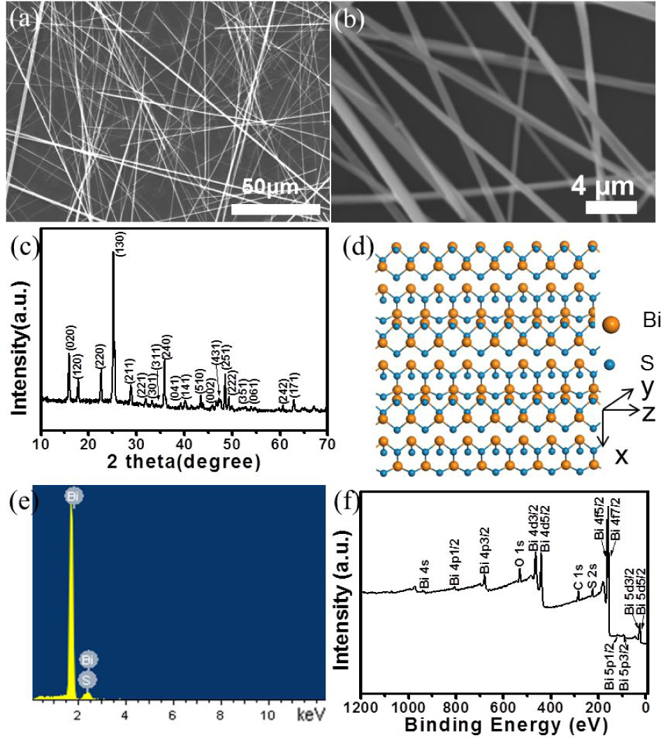
(a) Representative SEM image of the Bi2S3 NRs. (b) SEM image of the Bi2S3 NRs at large magnification. (c) XRD pattern of the Bi2S3 NRs. (d) Schematic illustration of the crystalstructure of the Bi2S3. (e) EDX spectrum of Bi2S3 NRs. (f) XPS spectrum analysis of the Bi2S3 NRs.

(a) TEM image of an individual Bi2S3 NR. (b) Corresponding HRTEM image. (c) and (d) elemental mapping of both S and Bi.
The microstructure of the as-prepared Bi2S3 NRs was then analyzed by both transmission electron microscopy (TEM) and high-resolution TEM. Figure 2a shows a typical TEM image of an individual Bi2S3 NR, in which the NR has a very smooth surface. The HRTEM image in Figure 2b exhibits a lattice-spacing of 0.38 nm, which corresponds to the d-spacing of (101) plane. Further analysis of the HRTEM image as well as the selected area electron diffraction (SAED) pattern reveals a preferential growth direction along [001], which agrees with previous report [31]. The EDS elemental mapping shows that the constituting elements (S and Bi atoms) were uniformed distributed in the NR (Figure 2c and d).
3 Results and discussion
Next, nano-photodetector based on individual Bi2S3 NR as shown in Figure 3(a) was fabricated to study its potential for device application. Figure 3(b) plots the typical I – V curves of an individual NR based photodetectors in dark and under 560 nm light illumination. It can be found that the I – V curves are linear at both conditions, suggesting that good contact (Ohmic contact) was formed at the In electrode/Bi2S3 NRs interface. When 560 nm light was illuminated on the photodetector, the current increased abruptly from 1.46 × 10⁻³ μA (corresponding to voltage of 2 V) to 0.215 μA, yielding an on/off ratio (i.e. photocurrent/dark current) of 147. Interestingly, with the increase of bias voltage, the photocurrent was observed to saturate when the voltage is as high as ∼14 V. It should be noted that the above photoresponse is highly reproducible when the illumination was repeatedly switched on and off. As shown in Figure 3(c), the photocurrent quickly increases to the maximum value and remains at a steady state upon light illumination. This process could be repeated with the light on and off for several cycles, indicative of good reproducibility of the photodetector device. To obtain a statistical significance, the dark current and photocurrent of 5 representative devices were plotted (Figure 3d). It is noted that all the devices exhibit obvious sensitivity to light illumination, with two lines denoting the average Idark and Ilight of 1.83 × 10⁻³, and 2.36 × 10⁻¹ μA, respectively. The large photocurrent is attributed to the photoconductive properties of Bi2S3 NRs upon 560 nm light illumination, whose energy is larger than the bandgap of the Bi2S3 NRs [32].
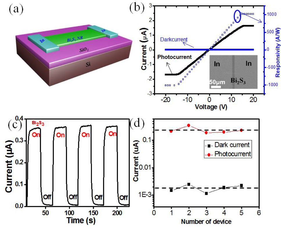
(a) Schematic illustration of the Bi2S3 NR device. (b) I – V curves and responsivity of Bi2S3 NR in dark and under 560 nm light illumination, the inset shows an SEM image of the device. (c) Photoresponsive characteristics of the Bi2S3 NR device. (d) Summary of both dark current and photocurrent of five representative individual Bi2S3 NR based device without HGNs decoration.
The inset of Figure 4(a) shows a typical TEM image of HGNs which were used to enhance the device performance of 1-D Bi2S3 NR device. In this study, the HGNs were synthesized by a sacrificial galvanic replacement reaction between Co nanoparticles and aqueous HAuC14[33], [34]. According to TEM analysis, their diameters are in the range from 20–40 nm, with average diameter of 30 nm (Figure 4b). What is more, the aspect ratio (i.e.: the inner-to-outer radius or din/douter) ranges from 20–80%, with a mean value of 55%. Theoretical simulation based on finite element method (FEM) reveals that for all HGNs with varied diameters (the aspect ratio is set to be 70%), the absorption spectrum exhibits strong absorption at 560 nm, which can be attributed to the LSPR of the HGNs. Moreover, the absorption intensity increases with the increasing diameter. This finding is understandable as large metal HGNs are capable of increasing the optical path length inside the nanostructures. Figure 4(d) plots the theoretical simulation of absorption of solid gold nanoparticles (SGN) and HGNs with aspect ratio ranging from 30–70%. Among the various HGNs with different diameters, SGNs show the weakest light absorption [35]. Meanwhile, when the aspect ratio increases gradually from 0 to 30, 50, 60, 70, and 75%, the wavelength of LSPR band is observed to red-shift from 500 to 505, 517, 531, 554, and 613 nm. In fact, the LSPR of the HGNs was experimentally confirmed by UV-vis absorption spectra of HGNs, Bi2S3 NRs and HGNs@Bi2S3 NRs, as shown in Figure 4(e). The absorption of pure Bi2S3 NRs is very weak at ∼570 nm. However, upon surface modification, the HGNs@Bi2S3 NRs heterojunction exhibits strong absorption at 570 nm, which corresponds to the LSPR band of HGNs.
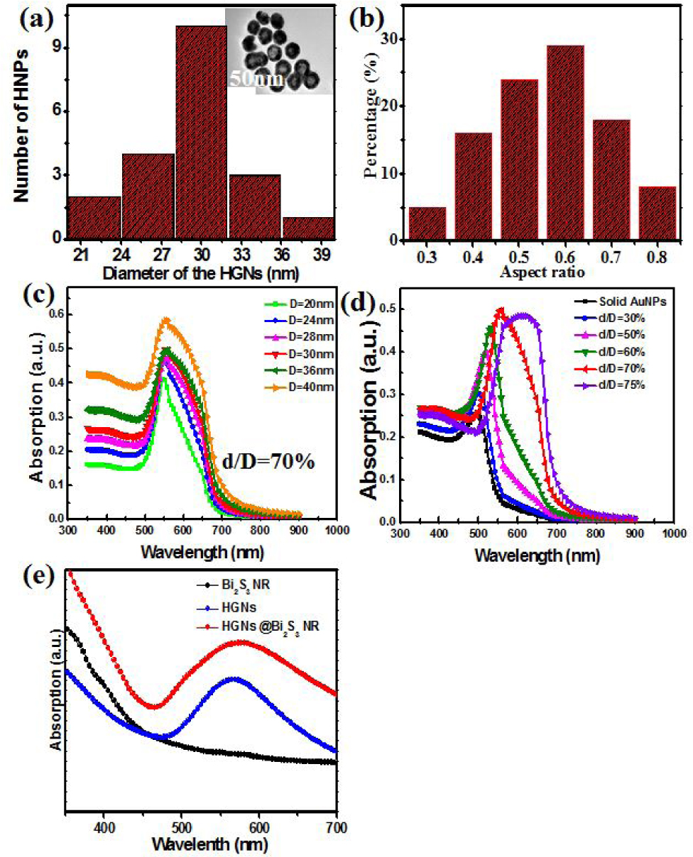
(a) Statistical distribution of the HGNs diameter. (b) The inner-to-outer radius aspect ratio of the HGNs. (c) Theoretical simulation of the HGNs with different diameters, the diameters are from 20 to 24, 28, 30, 36, and 40 nm. In addition, the inner-to-outer radius aspect ratios of all HGNs are set to be 70%. (d) Theoretical simulation of absorption of HGNs, the HGNs have inner-to-outer radius ratios ranging from 0 to 75%, the diameters of all nanoparticles (including both solid AuNPs and HGNs) are set to be 30 nm. (e) Experimental absorption spectra of Bi2S3 NRs, HGNs and HGNs @ Bi2S3 NRs.
The proof-of-concept plasmonic photodetector was fabricated by modifying HGNs on Bi2S3 NR surface via a simple chemical bonding method. Figure 5(a) illustrates the process to functionalize HGNs with ethylene glycol bis(3-mercaptopropionate), whose thiol groups (– SH) can bridge both Bi and Au atoms through chemical bonding. Optoelectronic study reveals that after HGNs decoration, the Bi2S3 NR device displays apparently enhanced sensitivity to light illumination. The photocurrent at bias voltage 2 V is about 1.66 μA, which is at least 6 times larger than that of device without HGNs [Figure 5(b)]. In addition, similar saturation in photocurrent was observed when the bias voltage was further increased. Our photoresponse study further suggests that the HGNs@Bi2S3 NR device is able to detect the illumination which was repeatedly switched on and off with good reproducibility [Figure 5(c)]. The dark current and photocurrent are 1.87 × 10⁻³ and 1.61 μA, respectively. Figure 5d lists the dark current and photocurrent of 5 representative HGNs@Bi2S3 NR devices. Compared with the device without HGNs (Figure 3d), the average photocurrent of HGNs@Bi2S3 NR increased from 2.36 × 10⁻¹ to 1.93 μA, while the dark current keeps nearly unchanged (Idark, Bi2S3/Idark, HGNs@Bi2S3:1.81 × 10⁻³ μA/1.83 × 10−3 μA), leading to considerable increase in On/Off ratio (from 147 to 1066).
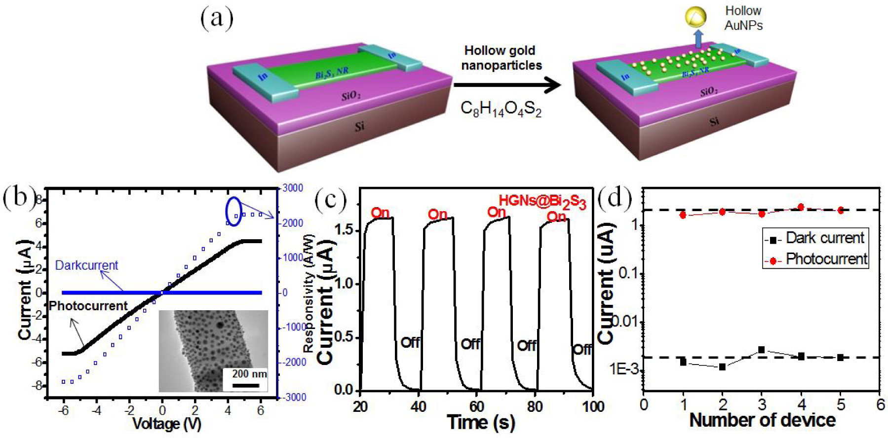
(a) Schematic illustration of the HGNs@Bi2S3 NR device. (b) I – V curves and responsivity of HGNs@Bi2S3 NR in dark and under 560 nm light illumination, the inset is the TEM image of a single NR modified with HGNs. (c) Photoresponsive characteristics of the HGNs@Bi2S3 NR device. (d) Summary of both dark current and photocurrent of 5 representative individual HGNs@Bi2S3 NR based device.
In order to quantitatively evaluate the performance of the present and other Bi2S3 nanostructures based devices, several key parameters including responsivity (R), conductivity gain (G), and detectivity (D) are calculated using the following equations:[36], [37]
Where Ip is the photo-excited current, Popt the incident light power illuminated on the device, h the Planck’s constant, c the velocity of the light, q the elemental charge, λ the incident light wavelength, η the quantum efficiency, A the effective area of the PD and Id the dark current, respectively. Based on the above equations, R is calculated to be 1.4 × 10² A/W (pure Bi2S3 NR) and 1.09 × 10³ A/W (HGNs@ Bi2S3 NR) under the illumination of 560 nm light at a bias of 2 V. G is estimated to be 2.68 × 10² (pure Bi2S3 NR) and 2.31 × 10³ (HGNs@ Bi2S3 NR). What is more, by assuming η = 1, D is determined to be 2.45 × 10¹² and 2.78 × 10¹³ Jones or Bi2S3 NRs and HGN@Bi2S3 NRs, respectively. Table 1 summarizes the several important metrics of our devices and other Bi2S3 nanostructures based photodetectors. Apparently, the key values of HGNs@Bi2S3 NRs were not only higher than photodetectors based on pure Bi2S3 NRs, but also than other Bi2S3 nanostructures based devices [21]. This result suggests that the utilization of the plasmonic HGNs is a promising method for improving the optoelectronic devices.
Comparison of the device performance of the present and other Bi2S3 nanostructures based photodetectors.
| Materials | On/off ratio | R/AW−1 | G | D* /cmHz1/2W−1 | Ref. |
|---|---|---|---|---|---|
| HGNs@Bi2S3 NR | 1066 | 1.09 × 10³ | 2.31 × 10³ | 2.78 × 10¹³ | our work |
| Bi2S3 NR | 147 | 1.4 × 10² | 2.68 × 10² | 2.45 × 10¹² | Our work |
| Bi2S3 crystalline | — | 1.7 | ∼40 | ∼1011 | [21] |
| Bi2S3 NW | 3.4 | — | — | — | [38] |
In addition to the high responsivity, conductive gain, and detectivity, the photocurrent of the plasmonic photodetector is highly dependent on the intensity of the excitation light. Figure 6 plots the photocurrents as a function of light intensity, from which one can find that the photocurrent increases almost linearly with increasing intensity. Carful fitting of both values finds that their relationship could be described by a power law [39]: I = APθ, where I, A, P and θ represent the photocurrent, the constant depending on the wavelength, the light power intensity and the exponent determining the response to light intensity, respectively. By fitting the curves, the θ for HGN@Bi2S3 NR is estimated to 0.96, slightly larger than that of pure Bi2S3 NR (0.91). Such a relatively large exponent is probably due to the passivation effect of the ethylene glycol bis(3-mercaptopropionate) during surface modification process. These nearly integer exponents for both devices are much larger than that of device composed of Bi2S3 nanocrystalline film (0.77),17 which means that the density of trapping center in both devices is very low according to Rose’s theory [40].
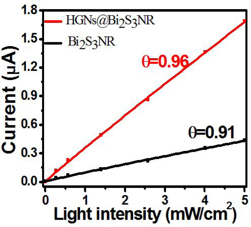
The fitting of the relationship between the photocurrent and light intensity for devices based on both pure Bi2S3 NR and HGNs@Bi2S3 NR.
The large enhancement of HGN@Bi2S3 NRS may be related to the strong LSPR, which is verified by FEM simulation. Figure 7 illustrates the electric field intensity distribution of the HGNs under light illumination with wavelengths of 350, 560 and 740 nm. Obviously, when shined by 560 nm light illumination, the HGNs can induce large-area hot spots with high field intensity. The peak dipolar electric energy according to the color bar, is more than 10-fold, which is much stronger than the ∼2.7-fold (350 nm) and 5.6-fold (740 nm), respectively. In addition, the field enhancement of HGNs under 560 nm light is much stronger than HGNs with the same diameter (5.1-fold). Such superb optical properties can be ascribed to their unique geometry: unlike the conventional solid gold nanoparticles with only one exterior surface, the HGNs have one more surface within the cavity. The two faces are able to facilitate coupling at light illumination, thus leading to relatively large field enhancement [41]. which is highly beneficial for light detection. Without question, compared with traditional plasmonic photodetectors using solid noble metal nanoparticles, the utilization of HGNs for enhancing nano-photodetector is advantageous in the following two aspects. (1) Large enhancement at low cost. Although the HGNs consume relatively few gold in comparison with SGNs, their field enhancement in contrast is much stronger. (2) Tunable LSPR band. As discussed above, the LSPR of HGNs can be easily adjusted in a range from 500–610 nm by tuning the aspect ratio. This convenience will make it possible to develop ultrasensitive nano-photodetectors with tunable spectral selectivity.
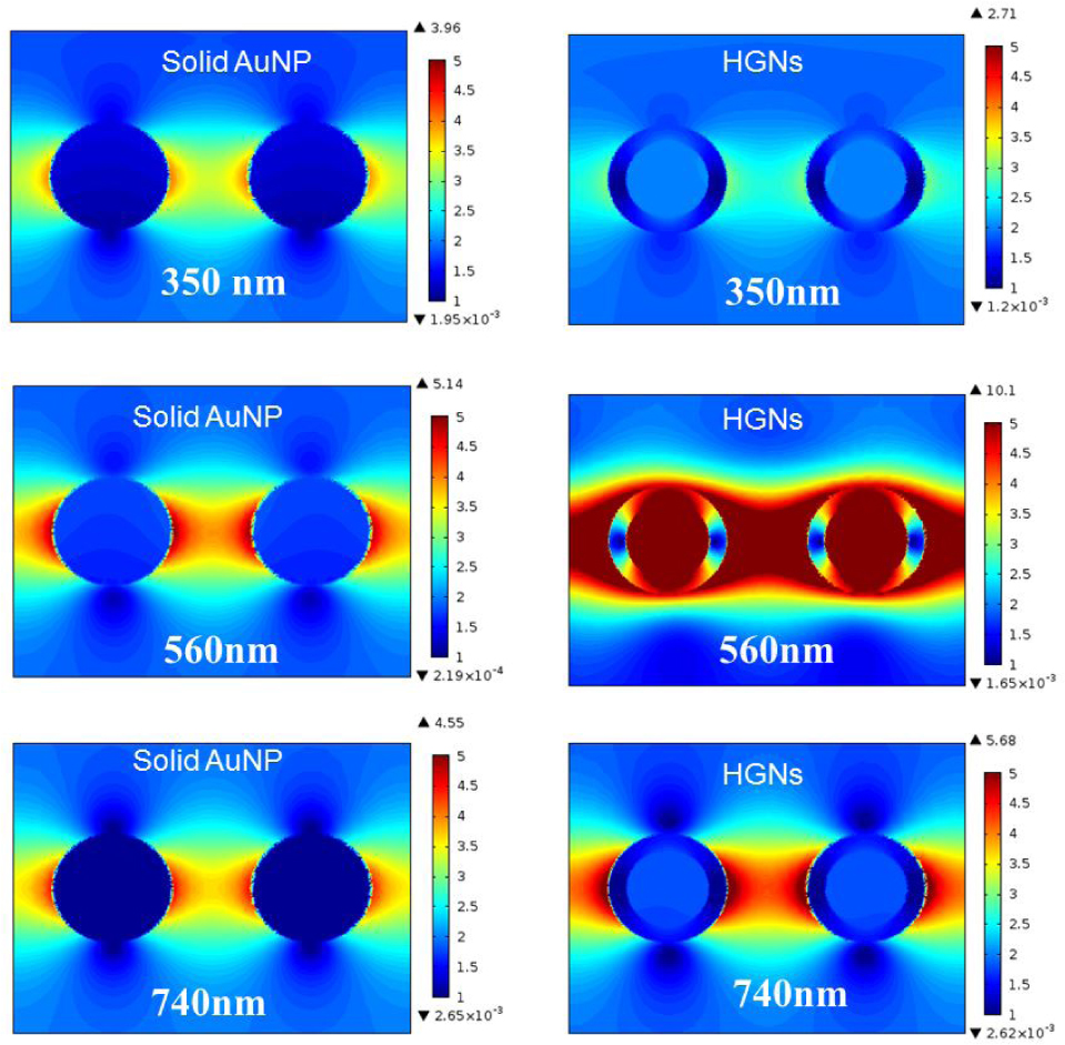
The electrical field distribution of both solid AuNP and HGNs under light illumination of 350, 560, and 740 nm. The solid AuNP has a diameter of 30 nm, and the HGN has a diameter and aspect ratio of 30 nm and 70%, respectively.
When the HGNs with strong LSPR effect were modified on the surface of Bi2S3 nanoribbons, the photocurrent, responsivity, and detectivity can be enhanced by the following three mechanisms: (1) Increased capability of light absorption by field enhancement. As a result, more photo-generated electron-hole pairs were generated, leading to enhanced photocurrent. (2) Accelerated separation of electron-hole pairs owning to the enhanced electromagnetic field surrounding the plasmonic HGNs [42], [43], [44]. (3) Direct electron transfer (DET). When irradiated by light illumination, the energetic hot electrons with energy as high as 1–4 eV will directly inject into the conduction band of the nearby semiconductor nanostructures [45], [46]. As a result, the photocurrent and responsivity were considerably increased.
4 Conclusion
In summary, we have demonstrated a simple strategy to improve the performance of nano-photodetector. The as-assembled HGN@Bi2S3 NR photodetector is highly sensitive to 560 nm illumination light with good reproducibility. Moreover, the HGNs decorated photodetector exhibits enhanced responsitivity, conductivity gain and detectivity in comparison with pure Bi2S3 NR and other Bi2S3 monocrystalline based devices. Theoretical simulation based FEM reveals that the enhancement in device performance is related to the LSPR effect of the HGNs, which may increase the light absorption of the HGNs@Bi2S3 NR heterojunction. This study suggests that plasmonic HGNs are highly reliable and efficient platforms to boost the device performance of 1-D semiconductor nanostructures based optoelectronic devices.
5 Methods
Synthesis and structural analysis of Bi2S3 NRS and hollow gold nanoparticles: The Bi2S3 NRs were synthesized via a simiple solvothermal approach. Briefly, NaOH, Bi(NO3)3, and Na2S2O3 were added sequentially into a mixed solution of glycerol and water (2:1 by volume), leading to a solution with concentration of 50 mM of Bi3+, 2 M of NaOH, and 100 mM of Na2S2O3. The mixed solution was then transferred into a Teflon-lined autoclave (50 mL capacity) which was sealed and maintained at 160°C. After keeping for 20 h, dark-gray precipate floating on the top of the solution was observed. The product was centrifuged and washed with distilled water for several times to remove possible contaminant and ions. The HGNs were prepared by a sacrificial galvanic replacement reaction between Co nanoparticles and aqueous HAuCl4. The Co nanoparticles were firstly synthesized by the following process: 1 M sodium borohydride solution (100 μL), 0.1 M trisodium citrate dehydrate (400 μL), 0.4 M cobalt hex-ahydrate solution (100 μL) and ultra-pure water (100 mL) were put into a three-neck flask and stirred to form a homogenous solution. To avoid the oxidation of the Co, the reaction solution was purged with N2 gas flow during the whole reaction process. After the formation of Co nanoparticles, 50 μl 0.1 M of chloroauric acid trihydrate solution was dropped into the above solution. Finally, the HGN was collected by centrifuging the HGN solution at 8000 rpm for 20 min. The phase of the Bi2S3 NR was examined using an X-ray diffraction (XRD, Rigaku D/Max-yB with Cu Kα radiation). The morphology and crystal structure were carried out on a SIRION 200 FEG scanning electron microscopy (FESEM), transmission electron microscopy (TEM), and high-resolution transmission electron microscopy (HRTEM, JEOL JEM-2010, at 200 kV). The optical absorption properties were performed on a UV-Vis absorption spectrophotometry (CARY 5000). The chemical composition of the product was analyzed using energy dispersive X-ray spectrometer (EDS), and X-ray photoelectron spectrometer (XPS).
Device construction and characterization: The Bi2S3 NRs based device was fabricated via the following procedures. Firstly, the as-synthesized Bi2S3 nanoribbons were dispersed on the SiO2 (300 nm)/Si substrate with a desired density. Then two parallel In electrodes were de-fined on the NR through a photolithography and e-beam evaporation method. Finally, to further decorate with hollow gold nanoparticles, the as-assembled device was immersed into an ethylene glycol bis(3-mercaptopropionate) solution for 1 h and HGN aqueous solution for 12 h sequentially. The optoelectronic properties of the fabricated photodetectors were measured on a Keithley 4200-SCSI-V system equipped with a monochromatic light source system (Princeton, ARC-SP-2155).
Theoretical simulation: The theoretical modeling was carried out by using a finite element method (FEM) to study the unit cell. A periodic boundary condition is used along x direction and transverse magnetic (TM) polarized light was assumed to be normally incident from the top of the structure. The calculated region is bordered by perfectly matched layers (PML) to reduce the influence of light reflection. The optical data of Au were from Sopra S. A. company database.
Acknowledgement
This work was supported by the Natural Science Foundation of China (NSFC, Nos. 61575059, 21501038, and 21101051), the Fundamental Research Funds for the Central Universities (2012HGCX0003, 2013HGCH0012, and 2014HGCH0005), the China Postdoctoral Science Foundation (103471013), and the Natural Science Foundation of Anhui Province (Grant No. J2014AKZR0036).
References
[1] Sudeep PK, Ipe BI, Thomas KG, George MV, Barazzouk S, Hotchandani S, Kamat PV. Fullerene-functionalized gold nanoparticles. A self-assembled photoactive antenna-metal nanocore assembly. Nano Lett 2002; 2: 29-35.10.1021/nl010073wSuche in Google Scholar
[2] Eustis S, El-Sayed MA. Why gold nanoparticles are more precious than pretty gold: Noble metal surface plasmon resonance and its enhancement of the radiative and nonradiative properties of nanocrystals of different shapes. Chem Soc Rev 2006;35:209-217.10.1039/B514191ESuche in Google Scholar PubMed
[3] Rasz S, Stenger N, Kadkhodazadeh S, Fischer SV, Kostesha N, Jauho AP, Burrows A, Wubs M, Mortensen NA. Blueshift of the surface plasmon resonance in silver nanoparticles studied with EELS. Nanophotonics 2013; 2:131-138.10.1515/nanoph-2012-0032Suche in Google Scholar
[4] Li RZ, Guo ZY, Wang W, Zhang JR, Zhang AJ, Liu JL, Qu SL, Gao J. Ultra-thin circular polarization analyzer based on the metal rectangular split-ring resonantors. Opt Express 2014; 22: 27968-27975.10.1364/OE.22.027968Suche in Google Scholar PubMed
[5] Wang W, Guo ZY, Li RZ, Zhang JR, Li Y, Liu Y, Wang XS, Qu SL, Plasmonics metalens independet from the incident polarizations. Opt Express 2015; 23: 16782-16791.10.1364/OE.23.016782Suche in Google Scholar PubMed
[6] Tian Y, Tatsuma T. Mechanisms and applications of plasmoninduced charge separation at TiO2 films loaded with gold nanoparticles. J Am Chem Soc 2005; 127: 7632-7.10.1021/ja042192uSuche in Google Scholar PubMed
[7] Wang P, Huang BB, Zhang XY, Qin XY, Jin H, Dai Y, Wang ZY, Wei JY, Zhan J, Wang SY, Wang JP, Whangbo MH. Highly efficient visible-light plasmonic photocatalyst Ag@AgBr. Chem Eur J 2009; 15: 1821-4.10.1002/chem.200802327Suche in Google Scholar PubMed
[8] Fang ZY, Fan LR, Lin CF, Zhang D, Meixner AJ, Zhu. X. Plasmonic coupling of bow tie antennas with Ag nanowire. Nano Lett 2011; 11: 1676-1680.10.1021/nl200179ySuche in Google Scholar PubMed
[9] Dorfmuller J, Cogelgesang R, Khunsin W, Rockstuhk C, Etrich C, Kern K. Plasmonic nanowire antennas: experiment, simulation, and theory. Nano Lett 2010; 10: 3596-3603.10.1021/nl101921ySuche in Google Scholar PubMed
[10] Ferry VE, Munday JN, Atwater HA. Design considerations for plasmonic photovoltaics. Adv Mater 2010; 22: 4794-4808.10.1002/adma.201000488Suche in Google Scholar PubMed
[11] Luo LB, Xie C, Wang XH, Yu YQ, Wu CY, Hu H, Zhou KY, Zhang XW, Jie JS. Surface plasmon resonance enhanced highly effi-cient planar silicon solar cell. Nano Energy 2014, 9:112-120.10.1016/j.nanoen.2014.07.003Suche in Google Scholar
[12] Okamoto K, Niki I, Shvartser A, Narukawa Y, Mukai T, Scherer A. Surface-plasmon-enhanced light emitters based on InGaN quantum wells. Nat Mater 2004; 3: 601-605.10.1038/nmat1198Suche in Google Scholar PubMed
[13] Chang CC, Sharma YD, Kim YS, Bur JA, Shenoi RV, Krishna S, Huang DH, Lin SY, A surface plasmon enhanced infrared photodetector based on InAs quantum dots. Nano Lett 2010, 10, (5), 1704-9.10.1021/nl100081jSuche in Google Scholar PubMed
[14] Luo LB, Zeng HL, Xie C, Yu YQ, Liang FX, Wu CY, Wang L, Hu JG. Light trapping and surface plasmon enhanced high-performance NIR photodetector. Sci Rep 2014; 4: 3914.10.1038/srep03914Suche in Google Scholar PubMed PubMed Central
[15] Buscema M, Groenendijk DJ, Blanter SI, Steele GA, van der Zant HSJ, Castellanos-Gomez A. Fast and broadband photoresponse of few-layer black phosphorus field-effect transistors. Nano Lett 2014; 14: 3347-3352.10.1021/nl5008085Suche in Google Scholar PubMed
[16] Tian W, Zhang C, Zhai TY, Li SL, Wang X, Liu JW, Jie X, Liu DQ, Liao MY, Koide Y, Golberg D, Bando, Y. Flexible ultraviolet photodetectors with broad photoresponse based on branched ZnS-ZnO heterostructure nanofilms. Adv Mater 2014; 26: 3088-3093.10.1002/adma.201305457Suche in Google Scholar PubMed
[17] Zhao HA, Guo QS, Xia FN, Wang H. Two-dimensional materials for nanophotonics application. Nanophotonics 2015; 4:128-142.10.1515/nanoph-2014-0022Suche in Google Scholar
[18] Liu KW, Sakurai M, Liao MY, Aono M. Giant improvement of the performance of ZnO nanowire photodetectors by Au nanoparticles. J Phys Chem C 2010, 114, 19835-9.10.1021/jp108320jSuche in Google Scholar
[19] Miao JS, Hu WD, Jing YL, Luo WJ, Liao L, Pan AL, Wu SW, Cheng JX, Chen XS, Lu W. Surface plasmon-enhanced photodetection in few layer MoS2 phototransistor with Au nanostructure array. Small 2015; 11: 2392-2398.10.1002/smll.201403422Suche in Google Scholar PubMed
[20] Li FZ, Luo LB, Huang XL, Yu YQ, Hu JG, Wu CY, Wang L, Zhu ZF, Jie JS, Yu SH. Ultrahigh mobility of p-type CdS nanowires: Surface charge transfer doping and photovoltaic devices. Adv Energy Mater 2013; 3: 579-583.10.1002/aenm.201200868Suche in Google Scholar
[21] Konstantatos G, Levina L, Tang J, Sargent EH. Sensitive solution-processed Bi2S3 nanocrystalline photodetectors. Nano Lett 2008; 8: 4002-6.10.1021/nl802600zSuche in Google Scholar PubMed
[22] Xie C, Nie B, Zeng LH, Liang FX, Wang MZ, Luo LB, Feng M, Yu YQ, Wu CY, Wu Y C, Yu SH. Core shell heterojunction of silicon nanowire arrays and carbon quantum dots for photovoltaic devices and self-driven photodetectors. ACS Nano 2014; 8: 4015-4022.10.1021/nn501001jSuche in Google Scholar PubMed
[23] Liu XQ, Liu X, Wang JL, Liao CN, Xiao XH, Guo SS, Jiang CZ, Fan ZY, Wang T, Chen XS. Transparent, high-performance thin-film transistors with an InGaZnO/aligned-SnO2-nanowire composite and their applicatio in photodetector. Adv Mater 2014; 26: 7399-7404.10.1002/adma.201401732Suche in Google Scholar PubMed
[24] Bao HF, Li CM, Cui XQ, Gan Y, Song QL, Guo J. Synthesis of a highly ordered single-crystalline Bi2S3 nanowire array and its metal/semiconductor/metal back-to-back Schottky diode. Small 2008; 4: 1125-9.10.1002/smll.200800007Suche in Google Scholar PubMed
[25] Ma JM, Yang JQ, Jiao LF, Wang TH, Lian JBA, Duan XC, Zheng WJ. Bi2S3 nanomaterials: morphology manipulation and related properties. Dalton T 2011; 40:10100-10108.10.1039/c1dt10846hSuche in Google Scholar PubMed
[26] Cademartiri L, Malakooti R, O’Brien PG, Migliori A, Petrov S, Kherani NP, Ozin GA. Large-scale synthesis of ultrathin Bi2S3 necklace nanowires. Angew Chem Int Ed 2008; 47: 3814-7.10.1002/anie.200705034Suche in Google Scholar PubMed
[27] Li HH, Yang J, Zhang JY, Zhou M. Facile synthesis of hierarchical Bi2S3 nanostructures for photodetector and gas sensor. RSC Adv 2012; 2: 6258-6261.10.1039/c2ra20751fSuche in Google Scholar
[28] Luo LB, Huang XL, Wang MZ, Xie C, Wu CY, Hu JG, Wang L, Huang JA. The effect of plasmonic nanoparticles on the optoelectronic characteristics of CdTe nanowires. Small 2014; 10: 2645-2652.10.1002/smll.201303388Suche in Google Scholar PubMed
[29] Nie B, Hu JG, Luo LB, Xie C, Zeng LH, Lv P, Li FZ, Jie JS, Feng M, Wu CY, Yu YQ, Yu SH. Monolayer graphene film on ZnO nanorod array for high-performance schottky junction ultraviolet photodetectors. Small 2013, 9, 2872-2879.10.1002/smll.201203188Suche in Google Scholar PubMed
[30] Liu ZP, Peng S, Xie Q, Hu ZK, Yang Y, Zhang SY, Qian YT. Large-scale synthesis of ultralong Bi2S3 nanoribbons via a solvothermal process. Adv Mater 2003; 15: 936-640.10.1002/adma.200304693Suche in Google Scholar
[31] Hu EL, Gao XH, Etogo A, Xie YL, Zhong YJ, Hu, Y. Controllable one-pot synthesis of various one-dimensional Bi2S3 nanostructures and their enhanced visible-light-driven photocatalytic reduction of Cr(VI). J Alloy Compd 2014; 611: 335-340.10.1016/j.jallcom.2014.05.075Suche in Google Scholar
[32] Zhang H, Ji YJ, Ma XY, Xu J, Yang DR. Long Bi2S3 nanowires prepared by a simple hydrothermal method. Nanotechnology 2003; 14: 974-7.10.1088/0957-4484/14/9/307Suche in Google Scholar
[33] Schwartzberg AM, Olson TY, Talley CE, Zhang JZ. Synthesis, characterization, and tunable optical properties of hollow gold nanospheres. J Phys Chem B 2006; 110: 19935-19944.10.1021/jp062136aSuche in Google Scholar PubMed
[34] Luo LB, Xie WJ, Zou YF, Yu YQ, Liang FX, Huang ZJ, Zhou KY. Surface plasmon propelled high-performance CdSe nanoribbons photodetector. Opt Exp 2015; 23:12979.10.1364/OE.23.012979Suche in Google Scholar PubMed
[35] Liang HP, Wan LJ, Bai CL, Jiang L. Gold hollow nanospheres: Tunable surface plasmon resonance controlled by interiorcavity sizes. J Phys Chem B 2005; 109: 7795-7800.10.1021/jp045006fSuche in Google Scholar PubMed
[36] Nie B, Luo LB, Chen JJ, Hu JG, Wu CY, Wang L, Yu YQ, Zhu ZF, Jie JS. Fabrication of p-type ZnSe:Sb nanowires for high-performance ultraviolet light photodetector application. Nanotechnology 2013; 24: 095603-710.1088/0957-4484/24/9/095603Suche in Google Scholar PubMed
[37] Wang MZ, Liang FX, Nie B, Zeng LH, Zheng LX, Lv P, Yu YQ, Xie C, Li YY, Luo LB. TiO2 nanotube array/monolayer graphene film schottky junction ultraviolet light photodetectors. Part Part Syst Char 2013, 30, 630-636.10.1002/ppsc.201300040Suche in Google Scholar
[38] Yang Q, Chen L, Hu CG, Wang SX, Zhang JC, Wu WD. Sensitive optical switch based on Bi2S3 single nanowire and nanowire film. J. Alloy Compd. 2014; 612: 301-5.10.1016/j.jallcom.2014.05.193Suche in Google Scholar
[39] Jie JS, Zhang WJ, Jiang Y, Meng XM, Li YQ, Lee ST. Photoconductive characteristics of single-crystal CdS nanoribbons. Nano Lett 2006; 9:1887-1892.10.1021/nl060867gSuche in Google Scholar PubMed
[40] Rose A. Concepts in photoconductivity and Allied Problems; Krieger Publishing Co.: New York, 1978.Suche in Google Scholar
[41] Liu KW, Sakurai M, Liao MY, Aono M. Giant improvement of the performance of ZnO nanowire photodetectors by Au nanoparticles. J Phys Chem C 2010; 114:198 35-198 39.10.1021/jp108320jSuche in Google Scholar
[42] Li DB, Sun XJ, Song H, Li ZM, Chen YR, Jiang H, Miao GQ. Realization of a high-performance GaN UV detector by nanoplasmonic enhancement. Adv Mater 2012; 24: 845-849.10.1002/adma.201102585Suche in Google Scholar PubMed
[43] Bao GH, Li DB, Sun XJ, Jiang MM, Li ZM, Song H, Jiang H, Chen YR, Miao GQ, Zhang ZW. Enhanced spectral resonse of an AlGaN-based solar-blind ultraviolet photodetector with Al nanoparticles. Opt Express 2014; 22: 24286-24293.10.1364/OE.22.024286Suche in Google Scholar PubMed
[44] Zhang W, Xu J, Li Y, Qi ZQ, Dai JN, Wu ZH, Chen CQ, Yin J, Li J, Jiang H, Fang YY. High-performance AlGaN metal-semiconductor-metal solar-blind ultraviolet photodetectors by localized surface plasmon enhancement. Appl Phys Lett 2015; 106: 021112-5.10.1063/1.4905929Suche in Google Scholar
[45] Linic P, Christopher P, Ingram DB. Plasmonic-metal nanostructures for efficient conversion of solar to chemical energy. Nat Mater 2011; 10: 911-921.10.1038/nmat3151Suche in Google Scholar PubMed
[46] Lee YK, Jung CH, Park J, Seo H, Somorjai GA, Park JY. Surface plasmon-driven hot electron flow probed with metal-semiconductor nanodiode. Nano Lett 2011; 11: 4251-4255.10.1021/nl2022459Suche in Google Scholar PubMed
© 2017 Feng-Xia Liang et al.
This work is licensed under the Creative Commons Attribution-NonCommercial-NoDerivatives 3.0 License.
Artikel in diesem Heft
- Review Articles
- Nonlinear optical interactions in silicon waveguides
- Progress in ultrafast laser processing and future prospects
- Toward biomaterial-based implantable photonic devices
- Progress and Prospects in Stretchable Electroluminescent Devices
- Traditional and emerging materials for optical metasurfaces
- Research Articles
- Lasing Enhanced Surface Plasmon Resonance Sensing
- Optical and Electronic Properties of Two-Dimensional Layered Materials
- Plasmonic hollow gold nanoparticles induced high-performance Bi2S3 nanoribbon photodetector
- Erratum
- Erratum to: Recent Progress on Plasmon-Enhanced Fluorescence