
Two simple ways of making clean nitrogen-doped graphene for TEM studies
-
Ivan Musil

 ,
Lennart Rieger
,
Lennart Rieger

Abstract
Graphene is the ideal transmission electron microscopy (TEM) support when it comes to imaging, but often offers poor interaction with samples due to its inert nature, making preparation of the TEM samples difficult. Graphitic nitrogen substitutions in graphene could boost its reactivity while simultaneously bringing minimal disturbance to its periodic structure. Here, two straightforward and easy to implement methods are shown for nitrogen doping of graphene that is already freely suspended on a TEM grid. One procedure utilizes a standard plasma cleaner capable of generating radio frequency plasma, for the other a simple direct current glow discharge plasma chamber was built. Successful implantation of graphitic nitrogen was achieved via both methods and verified by high resolution TEM. A series of experiments allowed to find satisfactory conditions for doping, yielding samples where nitrogen substitutions can be found and imaged within otherwise clean areas of graphene. Interaction of an adsorbate with graphitic nitrogen was observed on an atomic level, demonstrating its capability to bind other materials.
1 Introduction
Since its discovery in 2004, graphene has been the subject of intensive research as it holds promising perspectives for future applications and further exploration into the world of 2D materials [1], [2], [3], [4], [5]. In connection with low-voltage transmission electron microscopy (TEM), it is now routinely imaged not only for gaining new insights into its structure and properties [6], but more importantly, as a well defined test sample to evaluate the performance of a microscope [7], [8], [9], [10], [11], [12]. Furthermore, it is used to study effects of electron irradiation [13], [14], [15], [16], or it can serve as a supporting substrate for the structures to be imaged under the electron beam [17], [18], [19], [20], [21], [22], [23]. Moreover, bilayer graphene can stabilize the electron-beam sensitive materials and make their TEM investigations possible, see Ref. [24] for an overview. This does not come as a surprise, as graphene is the thinnest known material consisting of light atoms while displaying a high mechanical, chemical and thermal stability [25], [26], and a well ordered crystal structure that can be filtered out during postprocessing of the images if necessary. However, due to its chemically inert nature, many types of adsorbates (single atoms, organic molecules, biomolecules, nanoparticles) may stick only weakly to graphene’s surface. This makes the preparation of well dispersed objects on graphene difficult and could also lead to instabilities of the adsorbate during imaging. To overcome this hurdle, one could modify the chemical structure of graphene. Graphene oxide has been used as a hydrophilic support to allow imaging of biomolecules [27], but it comes with a loss of image quality compared to pristine graphene and is prone to charging due to its low conductivity [28], [29]. Another option is the introduction of defects to the graphene lattice (vacancy defects, grain boundaries, edges), which are known to attract various adsorbates like metal atoms [30], [31], [32], [33], [34], [35], organic molecules [36], [37] and even larger nanostructures [38], [39], [40]. Obviously, these defects will lead to irregularities inside the crystal structure, creating enough contrast change which could hamper interpretation of the image. Harnessing the reactive nature of such defects while simultaneously keeping the variance in contrast from the pristine lattice at a minimum, would open new pathways for the use of graphene as a supporting substrate for electron microscopy.
The introduction of dopant atoms could help in this regard, and nitrogen seems to be a promising candidate. In nitrogen doped (N-doped) graphene, the in-built nitrogen comes in several bonding variations, the most important ones being graphitic nitrogen (sp2-hybridized, bond to three carbon atoms), pyridinic nitrogen (sp2-hybridized, bond to two carbon atoms in six-membered ring) and pyrrolic nitrogen (sp3-hybridized, bond to two carbon atoms in five-membered ring). Especially interesting is the case of the graphitic nitrogen, as it brings minimal variation in contrast due to its similar atomic number compared to carbon and minuscule change in bond length [41]. Nitrogen species inside graphene have been shown to interact with metal atoms [42] and organic molecules [43], [44]. Furthermore, nitrogen doping can increase wettability of nanocarbons [45], [46] and it is assumed that by shifting the Fermi level through doping the hydrophilicity can be controlled [47].
Before using the advantages of N-doped graphene, it first needs to be produced. Considerable amount of research has been poured into understanding and controlling the amount and type of implanted nitrogen, as this can drastically change the chemical and physical characteristics of graphene [48], [49], [50]. However, there is still a long road ahead before achieving precise and easily implementable control of nitrogen implantation. There are generally two ways to carry out the doping, during chemical vapor deposition (CVD) growth of graphene or post-growth. While the former often works with nitrogen-containing precursors during CVD growth, which allows some control over the doping by guiding the chemical reactions taking place during the process, it is prone to growth-induced segregation effects, lacks spatial selectivity and has to be performed before further processing [51].
Post-synthesis doping, in contrast, is possible with any source of graphene, so that established growth recipes or commercial sources can be used. Many options are available for the bombardment of graphene with low energy nitrogen ions: treatment can either be done with a beam of ions [51], [52], [53], [54], [55], [56], [57] potentially with a spatial resolution down to a few nanometers [58] with focused ion beams, or with different types of plasma [42], [59], [60], [61], [62]. Control over the ion species, energies and dosage used could guide the implantation process into the desired direction. Full control over the process implies that one fully understands the interaction between ions and graphene, thus further and deeper research is needed at the basic level. To do so, it would be desirable to remove as many interfering factors as possible. The most suitable subject for this is freely-suspended graphene, as it is known that a substrate may influence the behavior of the ion interaction by changing the electronic and topological structure of graphene [63], [64], [65], [66] or by backscattering the ions and sputtering the underlying substrate atoms [67], [68], [69]. For example, Wilke et al. showed that an underlying SiC(0001) substrate has influence on the ordering of nitrogen defects inside graphene implanted at 25 eV ion energy [54]. Furthermore, the substrate can influence the properties of graphene, making it harder to determine the changes induced by doping. An often desired effect through doping is the enhancement of the electronic properties, but metallic [70], [71] as well as insulating [72], [73] substrates are able to induce a band gap in graphene by direct contact. Ion beam exposure was previously used to implant nitrogen into free-standing graphene [51], [53], [55], [56]. While ion accelerators allow well controlled exposure conditions, they require rather complex setups, involving ion deceleration and narrow ion distribution over energies, and the very low (few tens of eV) energies that are required for a high-rate creation of substitutional impurities [74]. Furthermore, it is often difficult to avoid creation of undesired defects, such as vacancies. In contrast, a plasma treatment also results in an exposure of the sample to low energy ions, although their energies are not so well defined. Different types of plasmas have been successfully used to introduce nitrogen into graphene. Most studies have used supported graphene, but plasma doping of freely-suspended graphene has also been reported [70], although such studies are rare. In particular, TEM imaging of individual nitrogen substitutions in the graphene lattice was not demonstrated in previous plasma doping experiments, so the detailed sample morphology remains unclear. Indeed, it appears that many doping procedures result in highly disordered carbon structures [75], while the aim of this work is to obtain nitrogen atoms integrated into a sufficiently regular graphene lattice to allow the imaging of individual impurities.
The methods used to examine N-doped graphene are as important as the doping methods themselves. Raman spectroscopy is often used in this regard, as it can be easily performed and gives information about the amount as well as nature (point defect, grain boundary, etc.) of defects in the graphene lattice [76], [77], [78]. Even some types of point defects can be distinguished to a certain extent [79]. However, Raman spectroscopy does not allow to discern between nitrogen defects or other types of point defects. Much deeper insight can be achieved by X-ray photoelectron spectroscopy (XPS), which reveals not only the elemental composition of the sample, but can even give information about the bonding state of the implanted nitrogen atoms. Although a powerful tool used in many doping experiments [60], [62], [80], [81], [82], [83], [84], [85], it is bound to give an overall highly resolved spectrum of the sample, but does not offer almost any spatial resolution. Furthermore, interpretation of the spectra can become quite challenging and there exist many different nitrogen species with close by binding energies, thus posing risks for false peak assignments [86]. Conventional Raman spectroscopy suffers from the same spatial resolution problem, whereby it is possible to identify single point defects using tip-enhanced Raman spectroscopy [87]. It is, however, exceptionally interesting to observe what it looks like in the vicinity of a nitrogen defect, as there may be other nitrogen and non-nitrogen point defects present close by, certain patterns in the arrangement of in-built nitrogens could be detected and the role of contamination better understood, which is known to have an impact on low energy ion implantation [54]. This can be achieved by high-resolution microscopy like scanning tunneling microscopy [54], [88], [89]. Electron microscopy is also capable of observing nitrogen inside graphene’s structure, a number of studies have been conducted with scanning transmission electron microscopy (STEM) [56], [57] and often combined with electron energy loss spectroscopy (EELS) [42], [53], [55], [90], [91]. Using high-resolution transmission electron microscopy (HRTEM), it is as well possible to identify and observe single graphitic nitrogen defects [41], while other nitrogen configurations can not be discerned from regular carbon-only defects. This approach is used here, as it allows a relatively quick survey of the sample, covering more area per exposure compared to STEM. Imaging the atomic environment around implanted nitrogen atoms provides an additional level of examination in this field. It offers a valuable contribution for the voyage towards chemically and electrically tailored graphene.
We applied several methods to dope free-standing graphene with nitrogen, which we were able to confirm with HRTEM. Doping was either conducted with radio-frequency (RF) plasma or with a simple gas direct current (DC) glow discharge plasma, denoted as method 1 and method 2, respectively. The latter method has not yet been reported for freely-suspended, monolayer graphene in literature to our knowledge. Monolayer graphene treated by either method is characterized for the first time with atomic resolution images of the nitrogen impurities. The recorded images were analyzed to determine process parameters for efficient nitrogen doping and the different approaches were compared with each other. A schematic drawing of all steps involved to prepare and examine the samples is shown in Figure 1. In this study we focused on the observation of graphitic nitrogen through HRTEM, Figure 2 shows a model of the expected structures in mono- and bilayer graphene.
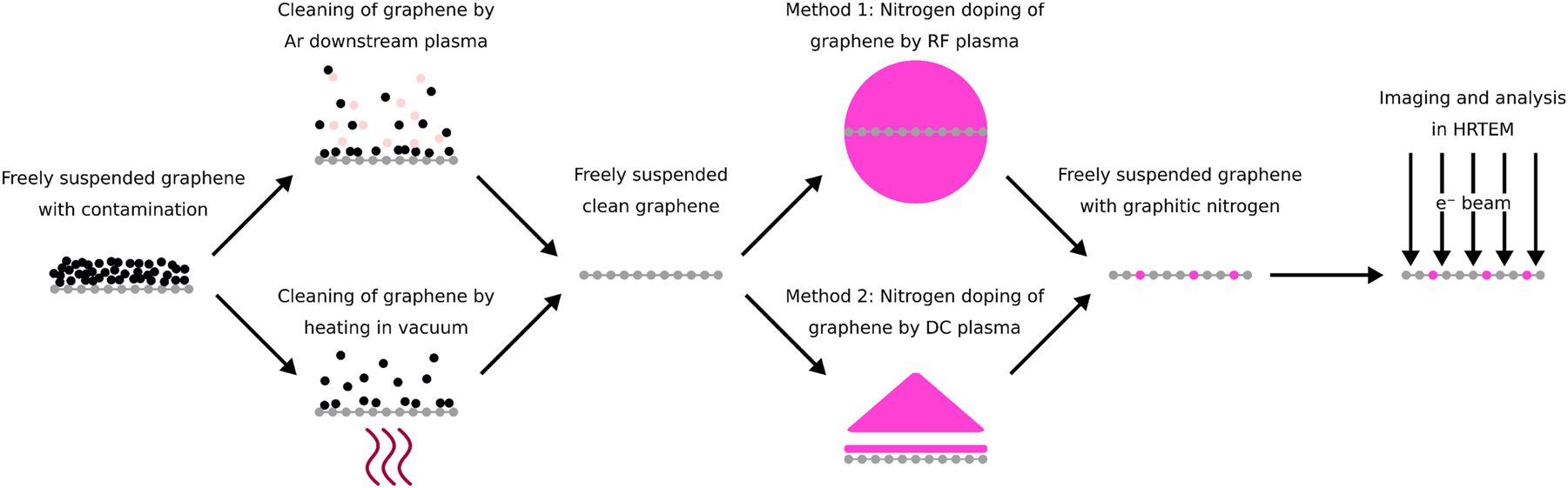
Schematic representation of steps used for preparing and analyzing nitrogen-doped graphene in this work. A more detailed description is found in Section 2.
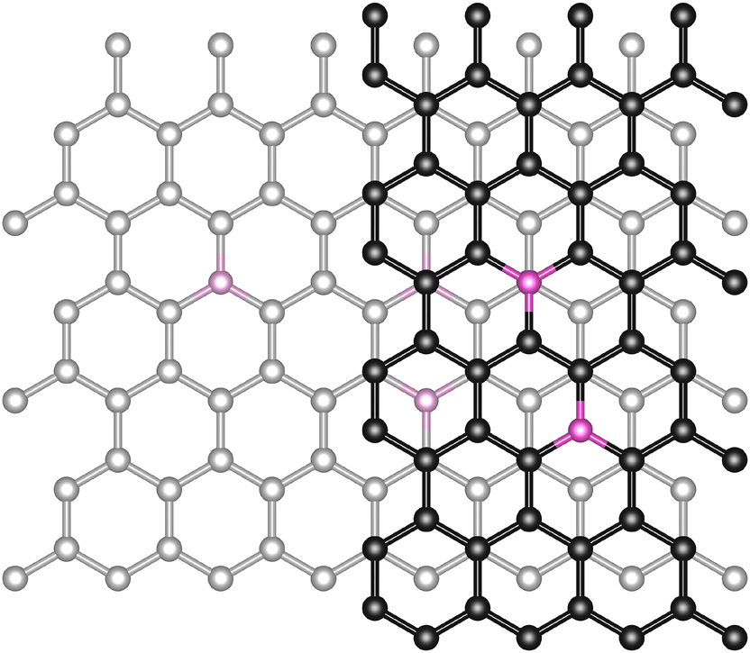
Schematic model of graphitic nitrogen implanted inside monolayer graphene (left) as well as bilayer graphene (right). Nitrogen atoms are highlighted in magenta. The darker lattice is the top layer.
2 Materials and methods
2.1 Sample preparation
Graphene monolayers on TEM grids were purchased from Graphenea, consisting of a gold TEM grid covered with a holey carbon film (Quantifoil) over which a monolayer CVD grown graphene is spanned. Cleaning of the samples was conducted either by downstream argon plasma in the Tergeo EM Plasma Cleaner or by heating to 450 °C at 0.1 mbar for 60 min.
2.2 Method 1: treatment of samples with RF plasma
Samples were treated with a Tergeo EM Plasma Cleaner from Pie Scientific, which is capable of generating a conductively coupled plasma at a frequency of 13.75 MHz. Doping was conducted with N2 gas. In addition, it can also create a downstream plasma, where ions are filtered out and only reactive species reach the sample. RF power, nitrogen flow and exposure time can be controlled to change the plasma properties and thus the treatment of each sample. Figure 3 shows an image and a schematic for both working modes of the plasma cleaner. RF1 and RF2 were cleaned by downstream argon plasma for 4 min. RF3 was cleaned by heating to 450 °C at 0.1 mbar for 60 min. The plasma at the position of the sample was characterized using a Langmuir probe method, as detailed in the supplementary information.
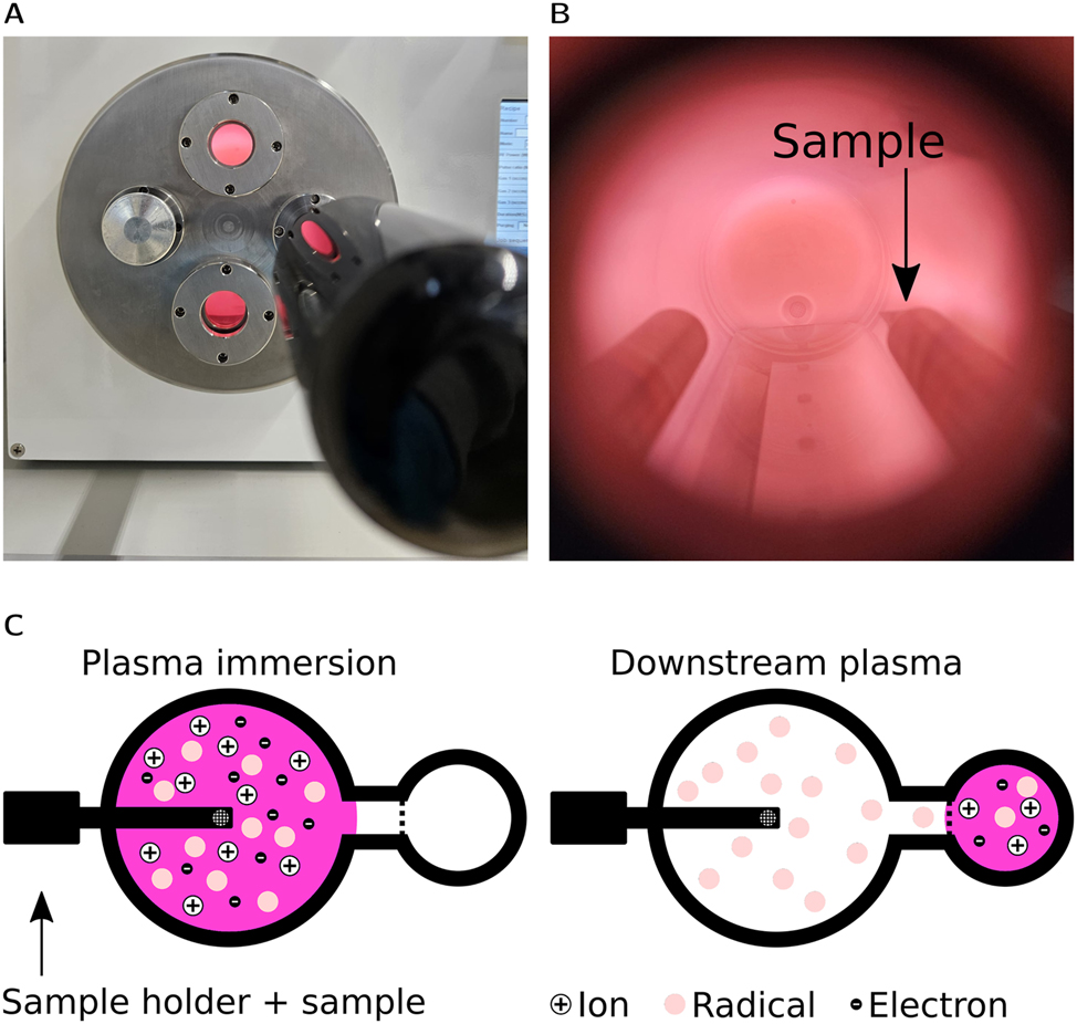
(A) Image of the plasma cleaner used in this work, with N2 plasma running and inserted TEM holder. (B) View through the window of the plasma cleaner, showing sample position. (C) Schematic drawing of immersion plasma mode (left) that is used to dope the sample and downstream plasma mode (right) that is used to clean the sample.
2.3 Method 2: treatment of samples with DC gas glow discharge plasma
DC plasma was realized by constructing a simple vacuum chamber, containing a copper rod as positive electrode and a sample holder as negative electrode (grounded), both being electrically connected to the outside and spaced by a distance of 15 mm from each other. Via two leakvalves, the chamber is connected to a Pfeiffer HiCube 300 turbopump station and the N2 gas line, allowing to adjust the desired pressure, which is monitored by a Pfeiffer CCR 363 pressure gauge (we note that a turbo pump is not strictly needed to obtain the pressures used in this study). A voltage of 750 V was applied to ignite the plasma inside the chamber, an exemplary photograph is shown in Figure 4A. Both sample holder and positive electrode were electrically connected to the outside and connected to a high voltage power supply (3B Scientific 5 kV power supply, adjustable from 0 to 5 kV, max. current 2 mA) power supply, as the scheme shows in Figure 4B. A relay driven by an Arduino microcontroller is used to switch the connection between the chamber and the power supply on for a selected amount of time, and thereby short pulses of discharges are obtained in a controlled way. The applied voltage was monitored via a multimeter. Most ions that strike the sample are created between the cathode and the negative glow region (see Figure 4B), thus only being accelerated by a part of the applied potential. All samples were cleaned by heating to 450 °C in a separate vacuum chamber at 0.1 mbar for 60 min prior to DC discharge plasma treatment.
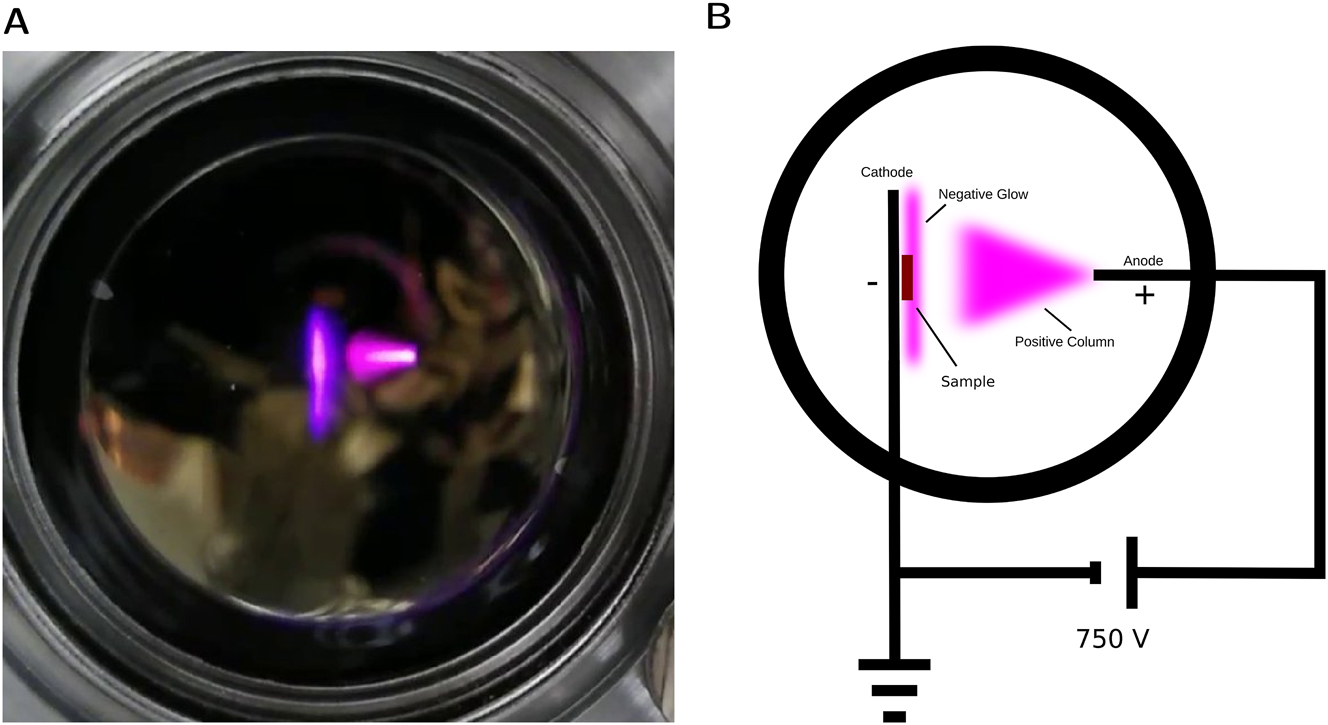
(A) Glow discharge inside DC plasma chamber at 6.5 mbar pressure and 750 V. (B) Sketch of observed glow discharge, showing electrical contacting and sample position.
2.4 TEM imaging and analysis
For HRTEM imaging an image-side corrected Jeol ARM200F TEM with CEOS aberration corrector and Gatan OneView camera was used at 80 kV acceleration voltage. Imaging and identification of the graphitic nitrogen substitution follows precisely the approach that was described previously [41], and is summarized here briefly: the contrast of the graphitic nitrogen is influenced by the rearrangement of charge density due to the perturbation of the electronic structure in the lattice by the nitrogen atom. As a result, it has a specific and rather unusual dependence on the defocus value, requiring optimized imaging conditions. Specifically, to enhance the contrast of the nitrogen defects, the defocus was set so that the graphene diffraction peaks were on the second ring of the contrast transfer function, i.e. the first zero crossing is just inside the six innnermost reflections. This corresponds to −18 nm defocus at 80 kV. After finding a suitable area to image, a series of roughly 30 images was taken to reach about 104 counts per pixel. For further analysis following procedure was applied using ImageJ: First the dark current reference was subtracted from the images and then they were divided by the gain reference. Intensity variations by slightly uneven illumination were removed by dividing each image by its strongly Gauss blurred duplicate. After aligning the series to compensate any drift, a summation or averaging of the series was done, resulting in a final image which could be further analyzed. As the contrast difference between a nitrogen defect and the pristine graphene lattice is minute, a Fourier transform of the image was created, the graphene peaks removed and a subsequent inverse Fourier transformation yielded a new image without crystal lattice. This way any defects are more easily visible in the image. The statistical analysis of graphitic nitrogens and other defects concentration was performed as follows: By measuring the size of the contamination-free area in each image, the number of carbon atoms for which individual point defects should be visible was estimated. The number of nitrogen or other defects in the same area was determined by simply counting them. Atomic concentrations were calculated by dividing the number of nitrogen or other defects by the number of expected carbon atoms. Three separate regions were imaged per sample and setting for statistical analysis. In the supplementary information, examples of the contrast analysis are given for the monolayer (as in the earlier study) and in comparison to the doped bilayer, which was not reported before.
3 Results
3.1 Radio-frequency plasma (method 1)
First attempts for nitrogen doping of graphene were done through the plasma cleaner. As the instrument is capable of a much higher plasma strength than needed, it was necessary to use it at very low power. Figure 5 shows an HRTEM image of one sample, where incorporated graphitic nitrogen as well as other defects are visible. Table 1 lists the parameters used for each sample. Using a higher power or longer exposure time lead to strong damaging or even complete removal of the graphene monolayer, thus these parameters were determined to be inside a suitable range for doping. Table 1 shows the determined graphitic nitrogen concentration as well as the concentration of other defects. As can be seen, nitrogen doping was achieved in all samples. Sample RF3 was subjected to an additional plasma cycle, in anticipation of a higher nitrogen concentration. However, the determined value seems to be even lower than before and strong damage of the sample was observed. Although the concentration of other defects is slightly higher than that of graphitic nitrogens in all samples, the latter can still be reliably found within the clean graphene sections of the sample.
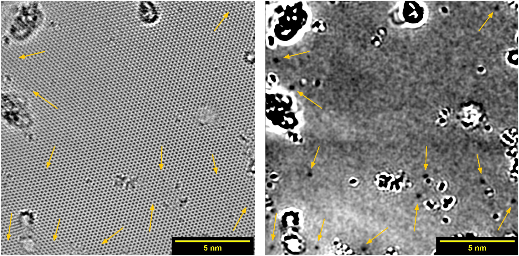
Monolayer graphene after doping with RF plasma, imaged by HRTEM (RF3). Arrows point at positions of graphitic nitrogen defects. On the left the complete image is shown, the same image with removed crystal lattice is shown on the right.
Results from RF plasma doping. Graphitic nitrogen and other defect concentrations determined by analysis of HRTEM images. For each sample all parameters (power, time, gas flow) used for doping are given. Note that RF3 was doped a second time, resulting in RF3-2.
| Sample | Parameters | Graphitic nitrogen concentration [at%] | Other defects concentration [at%] |
|---|---|---|---|
| RF1 | 1 W, 10 s, 1 sccm | 0.012 ± 0.012 | 0.021 ± 0.029 |
| RF2 | 1 W, 10 s, 50 sccm | 0.008 ± 0.012 | 0.029 ± 0.033 |
| RF3 | 1 W, 10 s, 25 sccm | 0.031 ± 0.011 | 0.071 ± 0.023 |
| RF3-2 | 1 W, 10 s, 25 sccm | 0.023 ± 0.017 | 0.034 ± 0.017 |
3.2 Direct current glow discharge plasma (method 2)
The plasma cleaner offers a quick and easy way to implant nitrogen inside graphene, but we achieved only relatively low doping concentrations. In search of a more suitable approach for doping, a DC glow discharge plasma chamber was built. The DC glow discharge is arguably the easiest way to create a plasma, probably even the first artificial one discovered as it has already been described by William Crookes in 1879 [92]. This low-effort and comparably cheap plasma chamber ionizes the incoming nitrogen gas by applying a high voltage between sample and an electrode, as seen in Figure 4. With this setup a series of doping experiments was conducted, using varying nitrogen gas pressures inside the chamber. Best results were achieved inside a pressure range from 3.5 to 8 mbar, higher pressures would either lead to strong contamination/destruction of the graphene or stable graphene with no incorporated nitrogen. Furthermore, it was found that short pulses of approximately 40 ms yield satisfactory and controllable results. Samples were also treated several times, first with 2 pulses, second time with 4 pulses and finally with additional 4 pulses. All parameters are shown in Table 2. Samples were observed via HRTEM and graphitic nitrogen could be found after doping, Figure 6 shows an example of such an image. In Figure 7 the measured concentration of graphitic nitrogen as well as other defects are visualized. As seen in Figure 7A, higher concentrations of graphitic nitrogen were achieved compared to the plasma cleaner method. Furthermore, with repeated treatment the graphitic nitrogen concentration increased, but at some point the graphene took up too much damage or got too contaminated to conduct further analysis. Only with 3.5 mbar we were able to still observe non-contaminated and free areas after 10 pulses. It seems that the graphitic nitrogen concentration reached a threshold at around 0.15 at%, before the destruction of bigger structures set in. Although the nitrogen content increased with further plasma treatment, it was not proportional to the number of applied pulses and the rise in concentration differed between the experiments. Here again, other defects were often in close vicinity to the graphitic nitrogen defects, as can be seen in Figure 6. For the 3.5 and 8 mbar series the number of defects outpaced the one of graphitic nitrogen or was similar, but the 5 and 6.5 mbar series showed higher amounts of graphitic nitrogen than other defects.
Results from DC plasma doping. Graphitic nitrogen and other defect concentrations determined by analysis of HRTEM images. For each sample N2 pressure and total number of pulses used for doping are given. Note that the same samples have been doped several times.
| Sample | Pressure [mbar] | Pulses | Graphitic nitrogen concentration [at%] | Other defects concentration [at%] |
|---|---|---|---|---|
| DC1 | 3.5 | 2 | 0.083 ± 0.011 | 0.099 ± 0.005 |
| DC1-2 | 3.5 | 6 | 0.120 ± 0.007 | 0.132 ± 0.036 |
| DC1-3 | 3.5 | 10 | 0.145 ± 0.006 | 0.100 ± 0.016 |
| DC2 | 5 | 2 | 0.133 ± 0.037 | 0.085 ± 0.017 |
| DC3 | 6.5 | 2 | 0.045 ± 0.016 | 0.015 ± 0.008 |
| DC3-2 | 6.5 | 6 | 0.133 ± 0.012 | 0.096 ± 0.048 |
| DC4 | 8 | 2 | 0.092 ± 0.004 | 0.126 ± 0.029 |
| DC4-2 | 8 | 6 | 0.103 ± 0.048 | 0.176 ± 0.007 |
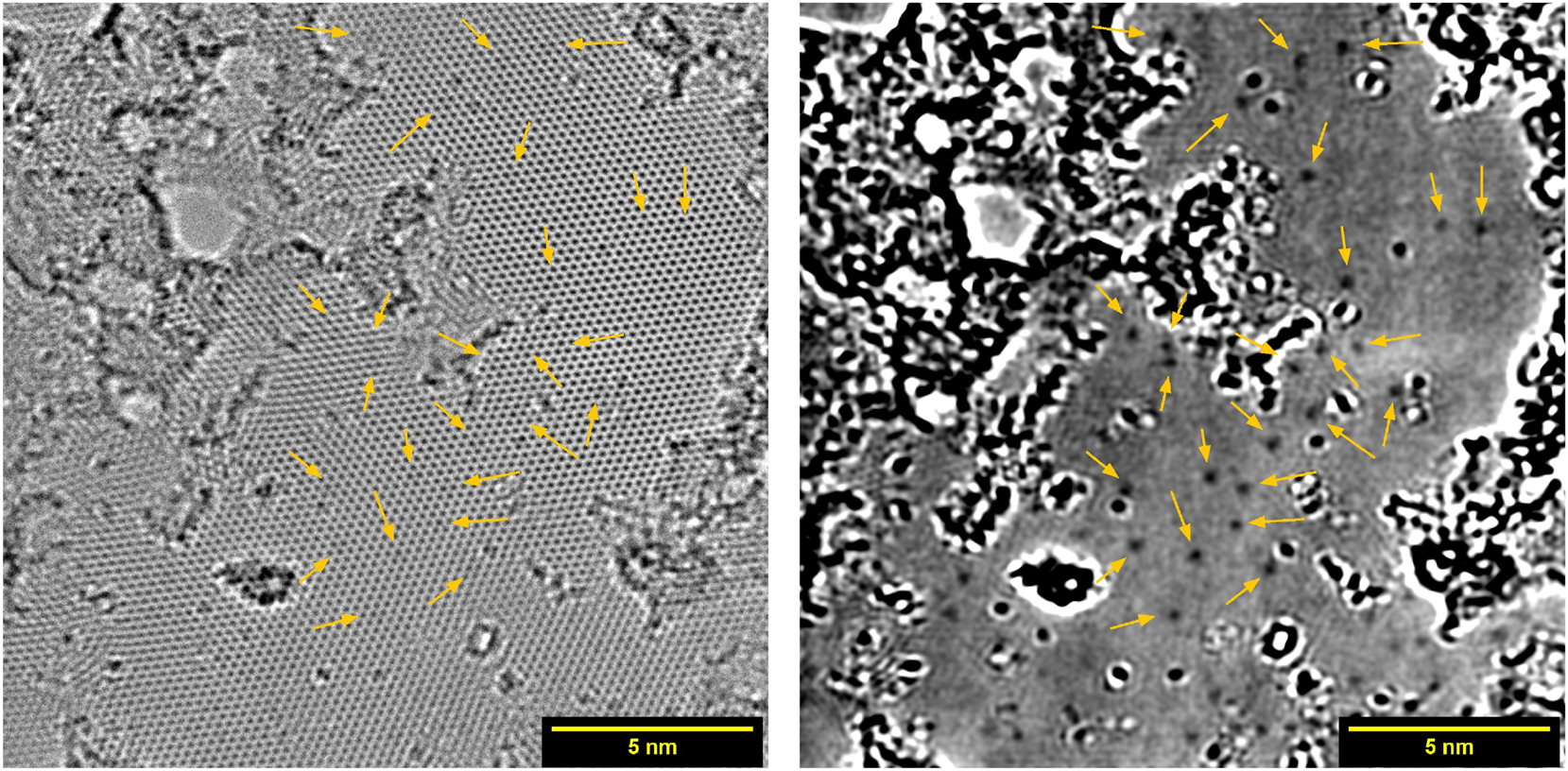
Monolayer graphene after doping inside DC plasma with 10 pulses at 3.5 mbar, imaged by HRTEM. Arrows point at positions of graphitic nitrogen defects. On the left the complete image is shown, the same image with removed crystal lattice is shown on the right.
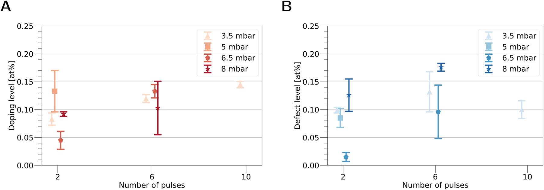
Results taken from Table 2. (A) Doping level of graphitic nitrogen as well as (B) defect level were determined from images.
3.3 Bilayer graphene doping
During imaging an area containing monolayer as well as bilayer graphene was found, as shown in Figure 8. Interestingly, graphitic nitrogen defects were detectable in both regions, as is shown in Figure S9.
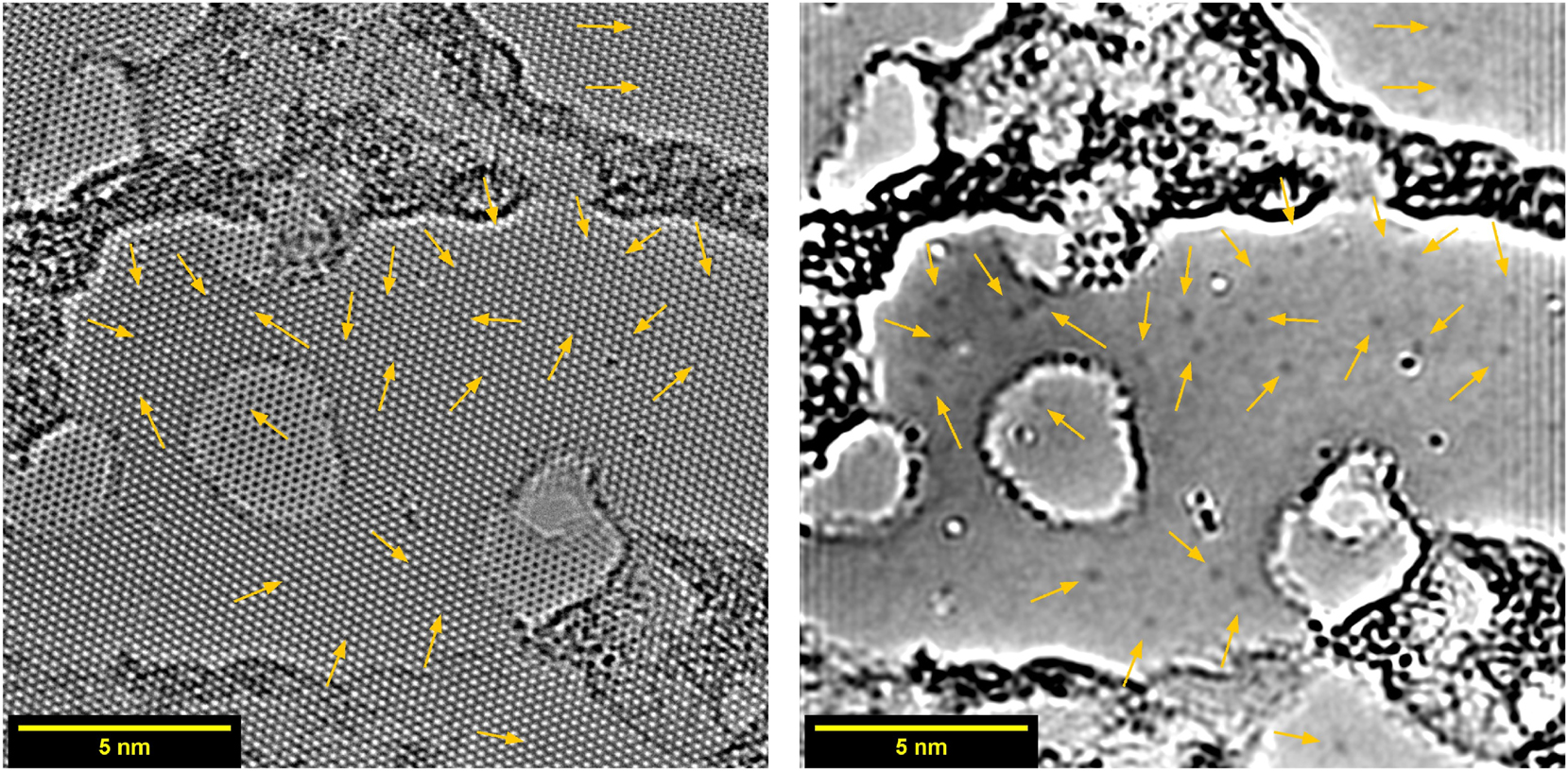
Bilayer graphene (most of the area) with some monolayer regions (holes formed in one of the two layers) after doping inside DC plasma with 2 pulses at 5 mbar, imaged by HRTEM. Arrows point at positions of graphitic nitrogen defects. On the left the original image is shown, the same image with removed crystal lattice is shown on the right.
3.4 Adsorption and desorption on a nitrogen substitution
During observation of a free area containing nitrogen defects, a different contrast was noticed temporarily for one of the graphitic nitrogens. Closer inspection revealed that only for a few frames of the image series an enhanced darker contrast was observable, whereas before and after the usual contrast value for graphitic nitrogen could be measured. Figure 9 shows three images from the series, where this change in contrast is visible. We interpret this as the temporary adsorption of heavier atom or small cluster at the nitrogen site, as discussed further below.
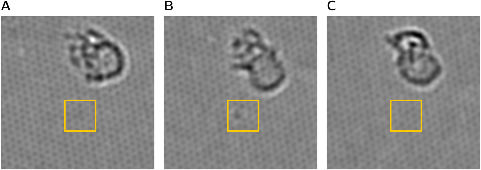
Observation of contrast change at position of a graphitic nitrogen defect, which is marked by the yellow box. Images show the nitrogen before (A), during contrast change (B) and afterwards (C). A slight Gauss blurring was applied to emphasize the change in contrast.
4 Discussion
4.1 Doping inside radio-frequency plasma (method 1)
Observing the results, as shown in Table 1, it is apparent that the concentration of graphitic nitrogen tends to stay below the concentration of other defects. This circumstance could be explained by the fact, that nitrogen defects are mostly created in a narrow range of ion energies [74], whereas other types of defects are more probable, e.g. vacancies at higher ion energies. Furthermore, it would be quite conceivable to conclude that some defects could be of pyrrolic or pyridinic nature. Unfortunately, these types can hardly be distinguished from simple vacancy defects inside the graphene lattice using HRTEM. It appears that a gas flow of 25 sccm introduces the highest number of defects (graphitic nitrogen and others), so that this setting could be just inside the right range for efficient doping of graphene. On one hand, a gas flow of 1 sccm might create too little ions due to the low gas pressure. On the other hand, 50 sccm might produce a too high pressure, thus hindering ions to accelerate and reach higher energies. Both, a too low ion concentration and energy, might lead to inefficient doping. However, from the characterization of the RF plasma (see Table S1) 1 sccm shows highest concentration in ions, contradicting this explanation. It should be kept in mind that the sample RF3 (25 sccm) was cleaned by heating in vacuum instead of downstream argon plasma, like RF1 and RF2 (1 and 50 sccm). Cleaning of the sample might have a significant impact on the implantation, as contamination that is already present before doping would shield the graphene from incoming nitrogen ions. Also, after doping contamination might preferably attach to more doped or defective regions, thereby hiding a portion of the dopant atoms in a selective way that affects the statistics.
A related study with freely-suspended graphene was conducted by Iyer et al. [70], where they used N2 RF plasma and analyzed the samples by X-ray and Raman spectroscopic methods. They were able to confirm different types of nitrogen species inside the sample, but no concentrations were determined. Compared to the results of this study, higher power (100 W) and longer exposure times (up to 10 min) were used. These values differ by orders of magnitude from the range of parameters determined here, outside of the range where we obtain stable structures. However, the power of the plasma source might not be directly comparable.
4.2 Doping inside direct current glow discharge plasma (method 2)
Higher graphitic nitrogen concentrations could be reached within the series of DC plasma doping experiments as compared to the RF plasma. However, there still seems to be a limit to the doping concentration that can be reached without destroying the sample or creating excessive other types of damage to the graphene. Similar to the RF plasma, it seems that doping is most efficiently achieved at medium pressures (5 and 6.5 mbar), at least in regards of the ratio between graphitic nitrogen and other defects. Again, the pressure inside the chamber might play an important role and can have an impact on the ion energy distribution. At too low pressure, the ion’s mean free path is big enough to accumulate more energy, making defects like single or double vacancies more probable. However, too high pressures should lead to lower ion energies and fewer number of defects of any kind, but this we can not observe in these results. It should be noted that only a small part of the possible parameter space could be explored in the scope of this study. For example, variation of the electrode geometry and applied voltage might lead to varying fractions of ions, radicals and neutrals bombarding the sample [93], [94]. Another relevant factor is the amount of hydrocarbons that is present inside the chamber during doping. By collisions with ions and neutrals these hydrocarbons might be deposited on the graphene as contamination and even turn at some point to amorphous carbon due to the energy transfer, similar to what happens under an electron beam. As noted before, contamination might shield the graphene from incoming ions, so that bakeout of the graphene in the same vacuum prior to doping would be desirable. However, examining the HRTEM images (Figures 5 and 6) reveals that many defects are in close vicinity to contamination. This circumstance might hint towards a deposition of contaminates after doping, possibly attracted by various defects.
A related study applying DC nitrogen plasma to multilayer graphene can be found in the literature, reaching doping concentrations of up to 3.12 at% [95]. In this case 350 V, 4.6 mbar and 20–40 s exposure time were used, which exceeds our time of 40 ms by magnitudes. However, the amount of graphitic nitrogen was not determined, and atomic level analysis (which would show the defectiveness of graphene besides the implanted nitrogen) is absent. In this case, 4–5 layer graphene on a substrate was used, which can be expected to withstand much harsher treatment conditions and is not easily comparable to freely-suspended graphene.
As discussed previously, HRTEM has some drawbacks when it comes to give a precise quantitative estimation for the nitrogen concentration of the samples. In particular, contamination accumulated during the transfer from DC chamber to the microscope might hide a portion of incorporated nitrogen atoms. However, in the case of doping graphene by ion implantation, contamination is also an often disregarded trap for other analysis methods. It is known that graphene tends to accumulate hydrocarbons from the air quite quickly [96]. Dedicated investigations have shown that the hydrocarbons themselves incorporate nitrogen atoms in a wide range of configurations, thus distorting the results obtained by commonly used methods as Raman spectroscopy and XPS [97]. Although often plagued by such contamination, HRTEM offers the possibility to truly confirm the integration of the nitrogen atom inside graphene’s structure. The samples obtained in this study display regions that are free from contamination, where nitrogen can be found surrounded by a clean lattice, for at least a significant fraction of the area. In spite of the doping, the overall appearance of clean regions interspersed with contamination networks is comparable to that of pristine graphene.
4.3 Doping and detection of nitrogen in bilayer graphene
As seen in Figure 8, graphitic nitrogen can be detected even in bilayer graphene. The defects show the same contrast in both mono- and bilayer (see Figure S9). However, we can not determine whether the nitrogen is preferentially implanted into one of the layers, as might be expected for the layer that points towards the other electrode in the DC discharge. It should be kept in mind that other doping mechanisms, involving chemical reactions with low energy ions, are theoretically conceivable [98]. A study of this aspect was conducted by Cress et al. on bilayer graphene [99]. They showed how low ion energies (45 eV) only modify the top layer, whereas higher energies (200 eV) modify both layers. As they used Raman spectroscopy to identify which layer is affected, there is no direct proof for the type of defect created.
4.4 Adsorption to graphitic nitrogen
As shown in Figure 9, a contrast change appears in the middle of the image series at the site of a graphitic nitrogen. Before as well as after this event the nitrogen defect was measurable at the exactly same position, thus it can be assumed that it is also present during the contrast change. Our explanation for this temporary increase in contrast is the presence of additional atoms, either a single adatom or several ones, possibly in the form of a molecule. From the image series it can be confirmed that the adsorption event goes on for roughly 60 s.
There are several theoretical studies concerned with the interaction and adsorption directly or close-by to graphitic nitrogen. Some state that the adsorption of various gases [100] and small hydrocarbons [101] is not enhanced by graphitic nitrogen, whereas many transition metals [101] and water [102] are supposed to bind more likely. Another theoretical study found that a carbon adatom, a likely species to encounter on graphene, would rather bind to the carbon neighbors of graphitic nitrogen than to itself [103]. This is explained by the charge redistribution introduced by the nitrogen, pushing more electron density towards the neighboring carbons and thus giving them a stronger electron donor character. Such change in electron density was confirmed experimentally by EELS [90], [91]. Scanning tunneling microscopy and spectroscopy experiments indicate that the interaction of certain organic molecules with graphene are manipulated by the presence of graphitic nitrogens [43], [44]. However, it is assumed that this results from the interaction with the changed electronic structure, rather than a chemical interaction with the nitrogen. Another study using STEM and EELS found no binding of various metal elements to graphitic nitrogen, but preferably to pyridinic nitrogen [42]. From these findings it could be assumed that graphitic nitrogen displays a weak binding character that is of electronic rather than of chemical nature.
The showcased images allow to observe a direct adsorption event mediated by graphitic nitrogen. Contrast change due to the adsorbate is visible directly at the nitrogen atom and its closer surroundings, making it hard to pin down which atoms participate during adsorption. Moreover, it is not clear if the interaction is of electronic or chemical character, but considering previous works, former might be more probable. This is also in line with the observation that no bonds are broken after the adsorbate has desorbed, leaving the graphitic nitrogen in the same configuration as before. However, our results indicate that graphitic nitrogen could have a higher affinity to adsorbates than previously expected.
4.5 N-doped graphene as substrate for TEM
As showcased before, graphitic nitrogen is able to adsorb atomic or molecular species for a time period which is sufficient for imaging. Of course the long-term stability of graphitic nitrogen under the electron beam is an important question. Indeed, the stability of the graphitic nitrogen substitution in graphene is remarkable, it is much more stable than most other defects under the 80 kV electron beam. Susi et al. showed that electron impact can displace a neighboring carbon atom, leading to the formation of pyridinic nitrogen [104]. However, this event is still quite rare at 80 kV and becomes more important at higher acceleration voltages. Another study by Warner et al. conducted at 60 kV concluded that graphitic nitrogen remains stable over a long time, even at temperatures of 500 °C [91]. This corresponds roughly to our findings, as many graphitic nitrogen defects would stay stable during recording of an image series, which could take more than 15 min. This time span should be enough for many applications, thus making N-doped graphene a suitable substrate for TEM. Another excellent characteristic of graphitic nitrogen is its very low contrast change compared to the pristine lattice, keeping the disturbance inside the image to a minimum. Other options for adsorption sites would be vacancy defects, but these bring stronger contrast change with them. Oxidative doping of graphene is another possibility to enhance adsorption [105], but oxygen defects often include some form of vacancy. There are records of triple bond oxygen in graphene [57], but it brings in more mass and charge compared with graphitic nitrogen, and this defect is also much less stable under the beam. Furthermore, oxidative doping usually demands high temperatures, which are often incompatible with most TEM holders. The plasma doping methods presented here can be applied directly at the TEM holder, keeping sample handling to a minimum. In general, both methods offer a simple, quick and controllable way to change the adsorption properties of graphene without greater disruption of its periodic structure inside the TEM image.
5 Conclusions
This work demonstrates successful N-doping of graphene by two simple methods, involving plasma treatment, one via a commercial plasma cleaner and another one via DC glow discharge plasma. Graphitic nitrogen inside structurally-intact graphene sheets was observed by HRTEM for both doping procedures. It was shown that detection of graphitic nitrogen is also possible in bilayer graphene. Furthermore, the direct binding of adsorbates to the graphitic nitrogen site was observed on an atomic scale.
These methods of graphene doping should be easy to implement for most labs and allow a chemical modification of graphene with minimal disturbance of its crystal structure, presenting an ideal TEM substrate with low background and enhanced binding of other materials to its surface. The N-doped graphene might also be used as a more interesting test sample than pristine graphene, providing a well defined structure with possibly the smallest contrast difference between neighboring atoms in a single atomic layer.
Funding source: Deutsche Forschungsgemeinschaft
Award Identifier / Grant number: KR 4866/9-1
Award Identifier / Grant number: ME 3313/6-1
Funding source: Vector Stiftung
Award Identifier / Grant number: P2022-0246
-
Research ethics: Not applicable.
-
Informed consent: Not applicable.
-
Author contributions: The authors have accepted responsibility for the entire content of this manuscript and approved its submission.
-
Use of Large Language Models, AI and Machine Learning Tools: None declared.
-
Conflict of interest: The authors state no conflict of interest.
-
Research funding: JCM and IM acknowledge funding from the Vector foundation, project No. P2022-0246, the German Research Foundation (DFG), project ME 3313/6-1, by the Ministry of Science, Research and Art Baden-Württemberg, Germany and by the European Union under EU-EFRE grant no. 712889. AVK acknowledges funding from the German Research Foundation (DFG), project KR 4866/9-1.
-
Data availability: The datasets generated and/or analyzed during the current study are available from the corresponding author on reasonable request.
References
[1] S. Roth and D. L. Carroll, “1 – Introduction to physics of low-dimensional systems,” in Graphene, 2nd ed., Woodhead Publishing Series in Electronic and Optical Materials, V. Skakalova and A. B. Kaiser, Cambridge, Woodhead Publishing, 2021, pp. 1–12.Search in Google Scholar
[2] F. Zhang, et al.., “Recent advances on graphene: synthesis, properties and applications,” Compos. Part A: Appl. Sci. Manuf., vol. 160, 2022, Art. no. 107051, https://doi.org/10.1016/j.compositesa.2022.107051.Search in Google Scholar
[3] A. R. Urade, I. Lahiri, and K. S. Suresh, “Graphene properties, synthesis and applications: a review,” JOM, vol. 75, no. 3, pp. 614–630, 2023, https://doi.org/10.1007/s11837-022-05505-8.Search in Google Scholar PubMed PubMed Central
[4] E. Galvagno, et al.., “Present status and perspectives of graphene and graphene-related materials in cultural heritage,” Adv. Funct. Mater., vol. 34, no. 13, 2024, Art. no. 2313043, https://doi.org/10.1002/adfm.202313043.Search in Google Scholar
[5] R. S. Perala, et al.., “A comprehensive review on graphene-based materials: from synthesis to contemporary sensor applications,” Mater. Sci. Eng. R: Rep., vol. 159, 2024, Art. no. 100805, https://doi.org/10.1016/j.mser.2024.100805.Search in Google Scholar
[6] G. Yang, L. Lihua, W. Bun, and M. C. Ng, “Structure of graphene and its disorders: a review,” Sci. Technol. Adv. Mater., vol. 19, no. 1, pp. 613–648, 2018, https://doi.org/10.1080/14686996.2018.1494493.Search in Google Scholar PubMed PubMed Central
[7] Z. Lee, J. C. Meyer, H. Rose, and U. Kaiser, “Optimum HRTEM image contrast at 20 kV and 80 kV—Exemplified by graphene,” Ultramicroscopy, vol. 112, no. 1, pp. 39–46, 2012, https://doi.org/10.1016/j.ultramic.2011.10.009.Search in Google Scholar PubMed
[8] W. Zhou, et al.., “Single atom microscopy,” Microsc. Microanal., vol. 18, no. 6, pp. 1342–1354, 2012, https://doi.org/10.1017/s1431927612013335.Search in Google Scholar PubMed
[9] L. Pardini, et al.., “Mapping atomic orbitals with the transmission electron microscope: images of defective graphene predicted from first-principles theory,” Phys. Rev. Lett., vol. 117, no. 3, 2016, Art. no. 036801, https://doi.org/10.1103/physrevlett.117.036801.Search in Google Scholar
[10] S. Morishita, M. Mukai, K. Suenaga, and H. Sawada, “Atomic resolution imaging at an ultralow accelerating voltage by a monochromatic transmission electron microscope,” Phys. Rev. Lett., vol. 117, no. 15, 2016, Art. no. 153004, https://doi.org/10.1103/physrevlett.117.153004.Search in Google Scholar PubMed
[11] O. L. Krivanek, et al.., “Improving the STEM spatial resolution limit,” Microsc. Microanal., vol. 24, no. S1, pp. 18–19, 2018, https://doi.org/10.1017/s1431927618000582.Search in Google Scholar
[12] F. Börrnert and U. Kaiser, “Chromatic- and geometric-aberration-corrected TEM imaging at 80 kV and 20 kV,” Phys. Rev. A, vol. 98, no. 2, 2018, Art. no. 023861, https://doi.org/10.1103/physreva.98.023861.Search in Google Scholar
[13] J. C. Meyer, et al.., “Accurate measurement of electron beam induced displacement cross sections for single-layer graphene,” Phys. Rev. Lett., vol. 108, no. 19, 2012, Art. no. 196102, https://doi.org/10.1103/physrevlett.108.196102.Search in Google Scholar
[14] G. T. Leuthner, et al.., “Scanning transmission electron microscopy under controlled low-pressure atmospheres,” Ultramicroscopy, vol. 203, pp. 76–81, 2019, https://doi.org/10.1016/j.ultramic.2019.02.002.Search in Google Scholar PubMed
[15] T. Susi, J. C. Meyer, and J. Kotakoski, “Quantifying transmission electron microscopy irradiation effects using two-dimensional materials,” Nat. Rev. Phys., vol. 1, no. 6, pp. 397–405, 2019, https://doi.org/10.1038/s42254-019-0058-y.Search in Google Scholar
[16] X. Zhao, et al.., “Engineering and modifying two-dimensional materials by electron beams,” MRS Bull., vol. 42, pp. 667–676, 2017, https://doi.org/10.1557/mrs.2017.184.Search in Google Scholar
[17] R. R. Nair, et al.., “Graphene as a transparent conductive support for studying biological molecules by transmission electron microscopy,” Appl. Phys. Lett., vol. 97, no. 15, 2010, Art. no. 153102, https://doi.org/10.1063/1.3492845.Search in Google Scholar
[18] B. Westenfelder, et al.., “Transformations of carbon adsorbates on graphene substrates under extreme heat,” Nano Lett., vol. 11, no. 12, pp. 5123–5127, 2011, https://doi.org/10.1021/nl203224z.Search in Google Scholar PubMed
[19] R. S. Pantelic, J. C. Meyer, U. Kaiser, and H. Stahlberg, “The application of graphene as a sample support in transmission electron microscopy,” Solid State Commun., vol. 152, no. 15, pp. 1375–1382, 2012, https://doi.org/10.1016/j.ssc.2012.04.038.Search in Google Scholar
[20] C. J. Russo and L. A. Passmore, “Modifying graphene substrates for imaging proteins in a transmission electron microscope,” Microsc. Microanal., vol. 20, no. S3, pp. 1214–1215, 2014, https://doi.org/10.1017/s1431927614007806.Search in Google Scholar
[21] J. Park, et al.., “Graphene liquid cell electron microscopy: progress, applications, and perspectives,” ACS Nano, vol. 15, no. 1, pp. 288–308, 2021, https://doi.org/10.1021/acsnano.0c10229.Search in Google Scholar PubMed
[22] S. Sinha and J. H. Warner, “Recent progress in using graphene as an ultrathin transparent support for transmission electron microscopy,” Small Struct., vol. 2, no. 4, 2021, Art. no. 2000049, https://doi.org/10.1002/sstr.202000049.Search in Google Scholar
[23] K. R. Strobel, et al.., “Temperature-dependence of beam-driven dynamics in graphene-fullerene sandwiches,” Micron, vol. 184, 2024, Art. no. 103666, https://doi.org/10.1016/j.micron.2024.103666.Search in Google Scholar PubMed
[24] A. V. Krasheninnikov, Y.-c. Lin, and K. Suenaga, “Graphene bilayer as a template for manufacturing novel encapsulated 2D materials,” Nano Lett., vol. 24, pp. 12733–12740, 2024, https://doi.org/10.1021/acs.nanolett.4c03654.Search in Google Scholar PubMed PubMed Central
[25] I. W. Frank, D. M. Tanenbaum, A. M. van der Zande, and P. L. McEuen, “Mechanical properties of suspended graphene sheets,” J. Vacuum Sci. Technol. B: Microelectron. Nanometer Struct. Process. Measur. Phenom., vol. 25, no. 6, pp. 2558–2561, 2007, https://doi.org/10.1116/1.2789446.Search in Google Scholar
[26] A. A. Balandin, et al.., “Superior thermal conductivity of single-layer graphene,” Nano Lett., vol. 8, no. 3, pp. 902–907, 2008, https://doi.org/10.1021/nl0731872.Search in Google Scholar PubMed
[27] R. S. Pantelic, J. C. Meyer, U. Kaiser, W. Baumeister, and J. M. Plitzko, “Graphene oxide: a substrate for optimizing preparations of frozen-hydrated samples,” J. Struct. Biol., vol. 170, no. 1, pp. 152–156, 2010, https://doi.org/10.1016/j.jsb.2009.12.020.Search in Google Scholar PubMed
[28] R. S. Pantelic, et al.., “Graphene: substrate preparation and introduction,” J. Struct. Biol., vol. 174, no. 1, pp. 234–238, 2011, https://doi.org/10.1016/j.jsb.2010.10.002.Search in Google Scholar PubMed
[29] C. Gómez-Navarro, et al.., “Electronic transport properties of individual chemically reduced graphene oxide sheets,” Nano Lett., vol. 7, no. 11, pp. 3499–3503, 2007, https://doi.org/10.1021/nl072090c.Search in Google Scholar PubMed
[30] Y. Gan, L. Sun, and F. Banhart, “One- and two-dimensional diffusion of metal atoms in graphene,” Small, vol. 4, no. 5, pp. 587–591, 2008, https://doi.org/10.1002/smll.200700929.Search in Google Scholar PubMed
[31] O. Cretu, et al.., “Migration and localization of metal atoms on strained graphene,” Phys. Rev. Lett., vol. 105, no. 19, 2010, Art. no. 196102, https://doi.org/10.1103/physrevlett.105.196102.Search in Google Scholar PubMed
[32] R. Zan, U. Bangert, Q. Ramasse, and K. S. Novoselov, “Interaction of metals with suspended graphene observed by transmission electron microscopy,” J. Phys. Chem. Lett., vol. 3, no. 7, pp. 953–958, 2012, https://doi.org/10.1021/jz201653g.Search in Google Scholar PubMed
[33] A. W. Robertson, et al.., “Dynamics of single Fe atoms in graphene vacancies,” Nano Lett., vol. 13, no. 4, pp. 1468–1475, 2013, https://doi.org/10.1021/nl304495v.Search in Google Scholar PubMed
[34] C. Gong, et al.., “Interactions of Pb and Te atoms with graphene,” Dalton Trans., vol. 43, no. 20, pp. 7442–7448, 2014, https://doi.org/10.1039/c4dt00143e.Search in Google Scholar PubMed
[35] Z. He, et al.., “Atomic structure and dynamics of metal dopant pairs in graphene,” Nano Lett., vol. 14, no. 7, pp. 3766–3772, 2014, https://doi.org/10.1021/nl500682j.Search in Google Scholar PubMed
[36] J. C. Meyer, C. O. Girit, M. F. Crommie, and A. Zettl, “Imaging and dynamics of light atoms and molecules on graphene,” Nature, vol. 454, no. 7202, pp. 319–322, 2008, https://doi.org/10.1038/nature07094.Search in Google Scholar PubMed
[37] F. Schäffel, M. Wilson, and J. H. Warner, “Motion of light adatoms and molecules on the surface of few-layer graphene,” ACS Nano, vol. 5, no. 12, pp. 9428–9441, 2011, https://doi.org/10.1021/nn2036494.Search in Google Scholar PubMed
[38] J. Choe, et al.., “Direct imaging of rotating molecules anchored on graphene,” Nanoscale, vol. 8, no. 27, pp. 13174–13180, 2016, https://doi.org/10.1039/c6nr04251a.Search in Google Scholar PubMed
[39] Q. Chen, K. He, A. W. Robertson, A. I. Kirkland, and J. H. Warner, “Atomic structure and dynamics of epitaxial 2D crystalline gold on graphene at elevated temperatures,” ACS Nano, vol. 10, no. 11, pp. 10 418–10 427, 2016, https://doi.org/10.1021/acsnano.6b06274.Search in Google Scholar PubMed
[40] S. Sinha, et al.., “In situ atomic-level studies of Gd atom release and migration on graphene from a metallofullerene precursor,” ACS Nano, vol. 12, no. 10, pp. 10439–10451, 2018, https://doi.org/10.1021/acsnano.8b06057.Search in Google Scholar PubMed
[41] J. C. Meyer, et al.., “Experimental analysis of charge redistribution due to chemical bonding by high-resolution transmission electron microscopy,” Nat. Mater., vol. 10, no. 3, pp. 209–215, 2011, https://doi.org/10.1038/nmat2941.Search in Google Scholar PubMed
[42] Y.-C. Lin, et al.., “Structural and chemical dynamics of pyridinic-nitrogen defects in graphene,” Nano Lett., vol. 15, no. 11, pp. 7408–7413, 2015, https://doi.org/10.1021/acs.nanolett.5b02831.Search in Google Scholar PubMed
[43] R. Lv, et al.., “Nitrogen-doped graphene: beyond single substitution and enhanced molecular sensing,” Sci. Rep., vol. 2, no. 1, p. 586, 2012, https://doi.org/10.1038/srep00586.Search in Google Scholar PubMed PubMed Central
[44] V. D. Pham, et al.., “Electronic interaction between nitrogen-doped graphene and porphyrin molecules,” ACS Nano, vol. 8, no. 9, pp. 9403–9409, 2014, https://doi.org/10.1021/nn503753e.Search in Google Scholar PubMed
[45] T. Matsuoka, H. Hatori, M. Kodama, J. Yamashita, and N. Miyajima, “Capillary condensation of water in the mesopores of nitrogen-enriched carbon aerogels,” Carbon, vol. 42, no. 11, pp. 2346–2349, 2004, https://doi.org/10.1016/j.carbon.2004.04.031.Search in Google Scholar
[46] A. D. Purceno, et al.., “Magnetic amphiphilic hybrid carbon nanotubes containing N-doped and undoped sections: powerful tensioactive nanostructures,” Nanoscale, vol. 7, no. 1, pp. 294–300, 2015, https://doi.org/10.1039/c4nr04005h.Search in Google Scholar PubMed
[47] G. Hong, et al.., “On the mechanism of hydrophilicity of graphene,” Nano Lett., vol. 16, no. 7, pp. 4447–4453, 2016, https://doi.org/10.1021/acs.nanolett.6b01594.Search in Google Scholar PubMed
[48] Z. Li and F. Chen, “Ion beam modification of two-dimensional materials: characterization, properties, and applications,” Appl. Phys. Rev., vol. 4, no. 1, 2017, Art. no. 011103, https://doi.org/10.1063/1.4977087.Search in Google Scholar
[49] X. Wu, X. Luo, H. Cheng, R. Yang, and X. Chen, “Recent progresses on ion beam irradiation induced structure and performance modulation of two-dimensional materials,” Nanoscale, vol. 15, no. 20, pp. 8925–8947, 2023, https://doi.org/10.1039/d3nr01366a.Search in Google Scholar PubMed
[50] B. Li, S. Zhang, C. Cui, W. Qian, and Y. Jin, “Comprehensive review on nitrogen-doped graphene: structure characterization, growth strategy, and capacitive energy storage,” Energy Fuels, vol. 37, no. 2, pp. 902–918, 2023, https://doi.org/10.1021/acs.energyfuels.2c03517.Search in Google Scholar
[51] M. Scardamaglia, et al.., “Nitrogen implantation of suspended graphene flakes: annealing effects and selectivity of sp2 nitrogen species,” Carbon, vol. 73, pp. 371–381, 2014, https://doi.org/10.1016/j.carbon.2014.02.078.Search in Google Scholar
[52] W. Zhao, et al.., “Production of nitrogen-doped graphene by low-energy nitrogen implantation,” J. Phys. Chem. C, vol. 116, no. 8, pp. 5062–5066, 2012, https://doi.org/10.1021/jp209927m.Search in Google Scholar
[53] U. Bangert, et al.., “Ion implantation of graphene—toward IC compatible technologies,” Nano Lett., vol. 13, no. 10, pp. 4902–4907, 2013, https://doi.org/10.1021/nl402812y.Search in Google Scholar PubMed
[54] P. Willke, et al.., “Short-range ordering of ion-implanted nitrogen atoms in SiC-graphene,” Appl. Phys. Lett., vol. 105, no. 11, 2014, Art. no. 111605, https://doi.org/10.1063/1.4895801.Search in Google Scholar
[55] D. Kepaptsoglou, et al.., “Electronic structure modification of ion implanted graphene: the spectroscopic signatures of p- and n-type doping,” ACS Nano, vol. 9, no. 11, pp. 11398–11407, 2015, https://doi.org/10.1021/acsnano.5b05305.Search in Google Scholar PubMed
[56] U. Bangert, et al.., “Ion-beam modification of 2-D materials – single implant atom analysis via annular dark-field electron microscopy,” Ultramicroscopy, vol. 176, pp. 31–36, 2017, https://doi.org/10.1016/j.ultramic.2016.12.011.Search in Google Scholar PubMed
[57] C. Hofer, et al.., “Direct imaging of light-element impurities in graphene reveals triple-coordinated oxygen,” Nat. Commun., vol. 10, no. 1, p. 4570, 2019, https://doi.org/10.1038/s41467-019-12537-3.Search in Google Scholar PubMed PubMed Central
[58] K. Höflich, et al.., “Roadmap for focused ion beam technologies,” Appl. Phys. Rev., vol. 10, no. 4, pp. 1–93, 2023, https://doi.org/10.1063/5.0162597.Search in Google Scholar
[59] Y. Shao, et al.., “Nitrogen-doped graphene and its electrochemical applications,” J. Mater. Chem., vol. 20, no. 35, pp. 7491–7496, 2010, https://doi.org/10.1039/c0jm00782j.Search in Google Scholar
[60] I. Bertóti, M. Mohai, and K. László, “Surface modification of graphene and graphite by nitrogen plasma: determination of chemical state alterations and assignments by quantitative X-ray photoelectron spectroscopy,” Carbon, vol. 84, pp. 185–196, 2015, https://doi.org/10.1016/j.carbon.2014.11.056.Search in Google Scholar
[61] G. R. S. Iyer, J. Wang, G. Wells, M. P. Bradley, and F. Borondics, “Nanoscale imaging of freestanding nitrogen doped single layer graphene,” Nanoscale, vol. 7, no. 6, pp. 2289–2294, 2015, https://doi.org/10.1039/c4nr05385k.Search in Google Scholar PubMed
[62] C. R. S. V. Boas, et al.., “Characterization of nitrogen doped graphene bilayers synthesized by fast, low temperature microwave plasma-enhanced chemical vapour deposition,” Sci. Rep., vol. 9, no. 1, 2019, Art. no. 13715, https://doi.org/10.1038/s41598-019-49900-9.Search in Google Scholar PubMed PubMed Central
[63] F. Varchon, et al.., “Electronic structure of epitaxial graphene layers on SiC: effect of the substrate,” Phys. Rev. Lett., vol. 99, no. 12, 2007, Art. no. 126805, https://doi.org/10.1103/physrevlett.99.126805.Search in Google Scholar PubMed
[64] T. Filleter and R. Bennewitz, “Structural and frictional properties of graphene films on SiC(0001) studied by atomic force microscopy,” Phys. Rev. B, vol. 81, no. 15, 2010, Art. no. 155412, https://doi.org/10.1103/physrevb.81.155412.Search in Google Scholar
[65] R. Villarreal, et al.., “Achieving high substitutional incorporation in mn-doped graphene,” ACS Nano, vol. 18, no. 27, pp. 17815–17825, 2024, https://doi.org/10.1021/acsnano.4c03475.Search in Google Scholar PubMed
[66] M. Kalbac, O. Lehtinen, A. V. Krasheninnikov, and J. Keinonen, “Ion-irradiation-induced defects in isotopically-labeled two layered graphene: enhanced in-situ annealing of the damage,” Adv. Mater., vol. 25, pp. 1004–1009, 2013, https://doi.org/10.1002/adma.201203807.Search in Google Scholar PubMed
[67] S. Kretschmer, et al.., “Supported two-dimensional materials under ion irradiation: the substrate governs defect production,” ACS Appl. Mater. Interfaces, vol. 10, no. 36, pp. 30827–30836, 2018, https://doi.org/10.1021/acsami.8b08471.Search in Google Scholar PubMed
[68] W. Li, X. Wang, X. Zhang, S. Zhao, H. Duan, and J. Xue, “Mechanism of the defect formation in supported graphene by energetic heavy ion irradiation: the substrate effect,” Sci. Rep., vol. 5, no. 1, p. 9935, 2015, https://doi.org/10.1038/srep09935.Search in Google Scholar PubMed PubMed Central
[69] E. A. Kolesov, “Choosing a substrate for the ion irradiation of two-dimensional materials,” Beilstein J. Nanotechnol., vol. 10, pp. 531–539, 2019, https://doi.org/10.3762/bjnano.10.54.Search in Google Scholar PubMed PubMed Central
[70] G. R. S. Iyer, et al.., “Large-area, freestanding, single-layer graphene–gold: a hybrid plasmonic nanostructure,” ACS Nano, vol. 8, no. 6, pp. 6353–6362, 2014, https://doi.org/10.1021/nn501864h.Search in Google Scholar PubMed
[71] J. Lee, K. S. Novoselov, and H. S. Shin, “Interaction between metal and graphene: dependence on the layer number of graphene,” ACS Nano, vol. 5, no. 1, pp. 608–612, 2011, https://doi.org/10.1021/nn103004c.Search in Google Scholar PubMed
[72] S. Y. Zhou, et al.., “Substrate-induced bandgap opening in epitaxial graphene,” Nat. Mater., vol. 6, no. 10, pp. 770–775, 2007, https://doi.org/10.1038/nmat2003.Search in Google Scholar PubMed
[73] R. Ribeiro-Palau, et al.., “Twistable electronics with dynamically rotatable heterostructures,” Science, vol. 361, no. 6403, pp. 690–693, 2018, https://doi.org/10.1126/science.aat6981.Search in Google Scholar
[74] S. Kretschmer and A. V. Krasheninnikov, “Atomistic simulations of low energy ion irradiation of 2D materials: from ab-initio molecular dynamics to simple binary collision model,” Phys. Rev. Mater., vol. 8, no. 11, 2024, Art. no. 114003, https://doi.org/10.1103/physrevmaterials.8.114003.Search in Google Scholar
[75] P. V. Pham, “A library of doped-graphene images via transmission electron microscopy,” C, vol. 4, no. 2, p. 34, 2018, https://doi.org/10.3390/c4020034.Search in Google Scholar
[76] R. Beams, L. Gustavo Cançado, and L. Novotny, “Raman characterization of defects and dopants in graphene,” J. Phys.: Condens. Matter, vol. 27, no. 8, 2015, Art. no. 083002, https://doi.org/10.1088/0953-8984/27/8/083002.Search in Google Scholar PubMed
[77] A. C. Ferrari and D. M. Basko, “Raman spectroscopy as a versatile tool for studying the properties of graphene,” Nat. Nanotechnol., vol. 8, no. 4, pp. 235–246, 2013, https://doi.org/10.1038/nnano.2013.46.Search in Google Scholar PubMed
[78] M. V. Bracamonte, G. I. Lacconi, S. E. Urreta, and L. E. F. Foa Torres, “On the nature of defects in liquid-phase exfoliated graphene,” J. Phys. Chem. C, vol. 118, no. 28, pp. 15455–15459, 2014, https://doi.org/10.1021/jp501930a.Search in Google Scholar
[79] A. Eckmann, et al.., “Probing the nature of defects in graphene by raman spectroscopy,” Nano Lett., vol. 12, no. 8, pp. 3925–3930, 2012, https://doi.org/10.1021/nl300901a.Search in Google Scholar PubMed
[80] H. Estrade-Szwarckopf, “XPS photoemission in carbonaceous materials: A “defect” peak beside the graphitic asymmetric peak,” Carbon, vol. 42, nos. 8-9, pp. 1713–1721, 2004, https://doi.org/10.1016/j.carbon.2004.03.005.Search in Google Scholar
[81] A. Barinov, et al.., “Initial stages of oxidation on graphitic surfaces: photoemission study and density functional theory calculations,” J. Phys. Chem. C, vol. 113, no. 21, pp. 9009–9013, 2009, https://doi.org/10.1021/jp902051d.Search in Google Scholar
[82] M. Cheng, et al.., “Restoration of graphene from graphene oxide by defect repair,” Carbon, vol. 50, no. 7, pp. 2581–2587, 2012, https://doi.org/10.1016/j.carbon.2012.02.016.Search in Google Scholar
[83] K. Ganesan, et al.., “A comparative study on defect estimation using XPS and Raman spectroscopy in few layer nanographitic structures,” Phys. Chem. Chem. Phys., vol. 18, no. 32, pp. 22160–22167, 2016, https://doi.org/10.1039/c6cp02033j.Search in Google Scholar PubMed
[84] W. Xie, L. Weng, K. L. Yeung, and C. Chan, “Repair of defects created by Ar+ sputtering on graphite surface by annealing as confirmed using ToF-SIMS and XPS,” Surf. Interface Anal., vol. 50, no. 9, pp. 851–859, 2018, https://doi.org/10.1002/sia.6487.Search in Google Scholar
[85] Y. Yamada, H. Tanaka, S. Kubo, and S. Sato, “Unveiling bonding states and roles of edges in nitrogen-doped graphene nanoribbon by X-ray photoelectron spectroscopy,” Carbon, vol. 185, pp. 342–367, 2021, https://doi.org/10.1016/j.carbon.2021.08.085.Search in Google Scholar
[86] T. Susi, T. Pichler, and P. Ayala, “X-ray photoelectron spectroscopy of graphitic carbon nanomaterials doped with heteroatoms,” Beilstein J. Nanotechnol., vol. 6, pp. 177–192, 2015, https://doi.org/10.3762/bjnano.6.17.Search in Google Scholar PubMed PubMed Central
[87] S. Mignuzzi, et al.., “Probing individual point defects in graphene via near-field Raman scattering,” Nanoscale, vol. 7, no. 46, pp. 19413–19418, 2015, https://doi.org/10.1039/c5nr04664e.Search in Google Scholar PubMed
[88] L. Zhao, et al.., “Visualizing individual nitrogen dopants in monolayer graphene,” Science, vol. 333, no. 6045, pp. 999–1003, 2011, https://doi.org/10.1126/science.1208759.Search in Google Scholar PubMed
[89] D. Deng, et al.., “Toward N-doped graphene via solvothermal synthesis,” Chem. Mater., vol. 23, no. 5, pp. 1188–1193, 2011, https://doi.org/10.1021/cm102666r.Search in Google Scholar
[90] R. J. Nicholls, et al.., “Probing the bonding in nitrogen-doped graphene using electron energy loss spectroscopy,” ACS Nano, vol. 7, no. 8, pp. 7145–7150, 2013, https://doi.org/10.1021/nn402489v.Search in Google Scholar PubMed
[91] J. H. Warner, Y.-C. Lin, K. He, M. Koshino, and K. Suenaga, “Stability and spectroscopy of single nitrogen dopants in graphene at elevated temperatures,” ACS Nano, vol. 8, no. 11, pp. 11806–11815, 2014, https://doi.org/10.1021/nn5054798.Search in Google Scholar PubMed
[92] W. Crookes, “On radiant matter; a lecture delivered to the British Association for the Advancement of Science, at Sheffield, Friday, August 22, 1879,” Am. J. Sci., vols. s3-18, no. 106, pp. 241–262, 1879, https://doi.org/10.2475/ajs.s3-18.106.241.Search in Google Scholar
[93] W. D. Davis and T. A. Vanderslice, “Ion energies at the cathode of a glow discharge,” Phys. Rev., vol. 131, no. 1, pp. 219–228, 1963, https://doi.org/10.1103/physrev.131.219.Search in Google Scholar
[94] K. S. Fancey and A. Matthews, “Some fundamental aspects of glow discharges in plasma-assisted processes,” Surf. Coat. Technol., vol. 33, pp. 17–29, 1987, https://doi.org/10.1016/0257-8972(87)90173-3.Search in Google Scholar
[95] W. Yang, et al.., “Nitrogen plasma modified CVD grown graphene as counter electrodes for bifacial dye-sensitized solar cells,” Electrochimica Acta, vol. 173, pp. 715–720, 2015, https://doi.org/10.1016/j.electacta.2015.05.143.Search in Google Scholar
[96] Z. Li, Y. Wang, et al.., “Effect of airborne contaminants on the wettability of supported graphene and graphite,” Nat. Mater., vol. 12, no. 10, pp. 925–931, 2013, https://doi.org/10.1038/nmat3709.Search in Google Scholar PubMed
[97] G. Robert Bigras, et al.., “Low-damage nitrogen incorporation in graphene films by nitrogen plasma treatment: effect of airborne contaminants,” Carbon, vol. 144, pp. 532–539, 2019, https://doi.org/10.1016/j.carbon.2018.12.095.Search in Google Scholar
[98] S. Moon, Y. Hijikata, and S. Irle, “Structural transformations of graphene exposed to nitrogen plasma: quantum chemical molecular dynamics simulations,” Phys. Chem. Chem. Phys., vol. 21, no. 23, pp. 12112–12120, 2019, https://doi.org/10.1039/c8cp06159a.Search in Google Scholar PubMed
[99] C. D. Cress, et al.., “Nitrogen-doped graphene and twisted bilayer graphene via hyperthermal ion implantation with depth control,” ACS Nano, vol. 10, no. 3, pp. 3714–3722, 2016, https://doi.org/10.1021/acsnano.6b00252.Search in Google Scholar PubMed
[100] J. Dai, J. Yuan, and P. Giannozzi, “Gas adsorption on graphene doped with B, N, Al, and S: a theoretical study,” Appl. Phys. Lett., vol. 95, no. 23, 2009, Art. no. 232105, https://doi.org/10.1063/1.3272008.Search in Google Scholar
[101] K. Li, N. Yan, T. Wang, Y. Zhang, Q. Song, and H. Li, “Adsorption of small hydrocarbons on pristine, N-doped and vacancy graphene by DFT study,” Appl. Surf. Sci., vol. 515, 2020, Art. no. 146028, https://doi.org/10.1016/j.apsusc.2020.146028.Search in Google Scholar
[102] T. Tan Pham, et al.., “How do the doping concentrations of N and B in graphene modify the water adsorption?,” RSC Adv., vol. 11, no. 32, pp. 19560–19568, 2021, https://doi.org/10.1039/d1ra01506k.Search in Google Scholar PubMed PubMed Central
[103] Z. Hou and K. Terakura, “Effect of nitrogen doping on the migration of the carbon adatom and monovacancy in graphene,” J. Phys. Chem. C, vol. 119, no. 9, pp. 4922–4933, 2015, https://doi.org/10.1021/jp512886t.Search in Google Scholar
[104] T. Susi, et al.., “Atomistic description of electron beam damage in nitrogen-doped graphene and single-walled carbon nanotubes,” ACS Nano, vol. 6, no. 10, pp. 8837–8846, 2012, https://doi.org/10.1021/nn303944f.Search in Google Scholar PubMed
[105] R. S. Pantelic, J. W. Suk, Y. Hao, R. S. Ruoff, and H. Stahlberg, “Oxidative doping renders graphene hydrophilic, facilitating its use as a support in biological TEM,” Nano Lett., vol. 11, no. 10, pp. 4319–4323, 2011, https://doi.org/10.1021/nl202386p.Search in Google Scholar PubMed
Supplementary Material
This article contains supplementary material (https://doi.org/10.1515/mim-2025-0014).
© 2025 the author(s), published by De Gruyter on behalf of Thoss Media
This work is licensed under the Creative Commons Attribution 4.0 International License.