Strengths and limitations of various analytical methods for all-solid state microbatteries
-
Berik Uzakbaiuly

 ,
Andre Borchers
,
Andre Borchers

Abstract
In this study, a comprehensive characterization of the commercially available all-solid-state battery (ASSB) was performed using various analytical techniques. SEM and EDX analyses revealed porosity in the Li1.3Al0.3Ti1.7(PO4)3 (LATP) electrolyte and Li3V2(PO4)3 (LVP) electrode, which hinders lithium-ion transport and affects electrochemical performance. ToF-SIMS confirmed a higher lithium concentration in the electrode compared to the electrolyte, while EBSD showed that the Cu current collector has randomly oriented grains, ensuring adequate electrical conductivity. AFM provided insights into surface morphology and potential distribution, confirming the effectiveness of ion polishing in sample preparation. Raman spectroscopy detected LATP electrolyte, indicating its potential use for process monitoring. Additionally, X-ray microscopy (XRM) enabled non-destructive imaging of the battery’s internal structure, although it was limited in resolving electrode and electrolyte layers. These findings contribute to a better understanding of solid-state battery design and highlight the strengths and limitations of various characterization techniques for performance optimization.
1 Introduction
All-solid-state batteries (ASSBs) have garnered significant attention in recent years due to their inherent safety, the potential to utilize metallic lithium (Li) for higher energy density, and the high ionic conductivity of solid electrolytes [1], [2]. However, different types of solid electrolytes suffer from distinct degradation mechanisms. Some experience Li dendrite formation [3], others develop interfacial layers between the solid electrolyte and metallic Li [4], and some exhibit microcracking during cycling [5]. These challenges have driven research into various solutions for ASSBs. Approaches include stabilizing the interfacial layer through doping, introducing buffer layers – either polymeric or ceramic – between the electrolyte and electrode, and designing composite electrodes or electrolytes [6].
Despite these issues, ASSBs have found niche applications, particularly in miniaturized energy storage [7]. Microbatteries are used in Internet of Things (IoT) devices, smart microelectronics, RFID tags, smart cards, Bluetooth beacons, and more [7], [8]. The success of these applications is largely due to the well-established lithium phosphorus oxynitride (LiPON) solid electrolyte, developed at Oak Ridge National Laboratory, which is stable against metallic Li [9]. Other solid electrolytes, such as garnet-type Li7La3Zr2O12, sulfide-based Li6PS5Cl, and NASICON-type Li1.3Al0.3Ti1.7(PO4)3 (LATP), are also being explored. Notably, LATP has gained attention due to its relative stability in air, making it easier to handle [10].
One notable commercialized microbattery is TDK Corp.’s Ceracharge™, which utilizes LATP as the electrolyte [11]. This microbattery, with a nominal voltage of 1.5 V and a capacity of 100 μAh, is compatible with solder reflow processes. Additionally, its bipolar electrode, Li3V2(PO4)3 (LVP), functions as both a cathode and an anode [12]. This dual functionality is enabled by vanadium’s multiple oxidation states (V2+, V3+, V4+, V5+), which allow reversible lithium insertion/extraction across a wide voltage window ranging approximately from 0.5 V to 4.3 V versus Li+/Li. The robust phosphate framework of LVP prevents significant volume expansion, enabling stable cycling. CeraCharge™ employs a multilayer design analogous to multilayer ceramic capacitors, consisting of stacked LVP electrode layers and LATP electrolyte layers (Figure 1).
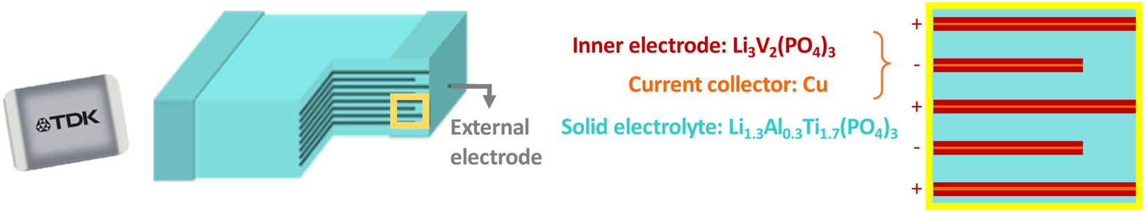
TDK ceracharge battery with schematics of internal multilayered structure.
This innovative battery has been explored for applications such as micro-pills [13], DC-DC converters [14], on-chip power harvesting [15], and power management [16]. Recently, Johnson et al. used computed tomography with deep learning algorithms to analyze these batteries more efficiently, overcoming resolution limitations caused by fast scans [17]. Computed tomography is a powerful non-destructive analysis tool, and its integration with complementary techniques enhances battery characterization.
In this study, we present a comprehensive characterization of the CeraCharge battery using multiple analytical techniques, including scanning electron microscopy (SEM), energy dispersive X-ray spectroscopy (EDX), electron backscatter diffraction (EBSD), Time-of-flight secondary ion mass spectrometry (ToF-SIMS), micro-computed tomography (μCT), atomic force microscopy (AFM), and Spontaneous Raman spectroscopy. The obtained data were correlated to highlight the strengths and limitations of each technique, offering a framework for the characterization of both miniaturized and conventional ASSBs.
2 Materials and methods
2.1 Sample preparation
TDK CeraCharge samples (BCT1812) were acquired from a single batch and used as-is for μCT characterization. For other characterization techniques, the samples were cut using a diamond cutter and subsequently polished with 15 μm, 9 μm, and 2 μm grained diamond foils (Type U) using an EM TXP target preparation device (Leica Microsystems) in an Ar-filled glovebox. Further polishing was performed using an 8 kV, 3 mA Ar ion beam with an EM TIC 3× ion beam milling system (Leica Microsystems). All sample transfers between instruments were conducted using the EM VCT500 vacuum cryo transfer system (Leica Microsystems), ensuring no exposure to air. Throughout the handling process inside the glovebox, H2O and O2 levels were maintained below 0.1 ppm.
2.2 Sample characterization
The samples were characterized using various methods. High-resolution images were obtained using Scanning Electron Microscopy (SEM, Zeiss Crossbeam 550) with a focused electron beam at 5 kV (gun voltage) and 100 pA (probe current). The in-lens detector provided high-resolution imaging of fine surface details, while the Secondary Electrons Secondary Ions (SESI) detector allowed for imaging with contrast control. The images were processed with ImageJ (1.54f) software for thickness measurements.
To analyze the elemental composition, a high-energy electron beam (10 kV, 1 nA) interacted with the sample, emitting characteristic X-rays that were captured by the EDX detector (Oxford Instruments). The crystallographic structure of the Cu layer was examined using Electron Backscatter Diffraction (EBSD, eFlash Bruker) at 20 kV and 2 nA, with the sample tilted 70° towards the EBSD detector. The EBSD resolution was set to 170×128 pixels per frame.
For Time-of-Flight Secondary Ion Mass Spectrometry (ToF-SIMS, Tofwerk AG), the sample was bombarded with Ga ions from an FIB gun operating at 30 kV and 700 pA. The resulting secondary ions were analyzed based on their time of flight to determine their mass-to-charge ratio.
Non-destructive micro-computed tomography (μCT, Zeiss Versa 620) was used to capture detailed 3D images of the internal and external structures of the sample using X-rays (140 kV, 21 W). The images were reconstructed from 1,601 projections, and subsequent analysis was performed using XamFlow (Lucid Concepts AG) software. The pixel size for the overview scan was 3.6 μm and for the detailed scan was 0.28 μm.
Atomic Force Microscopy (AFM, Park Systems NX10 installed in the Ar-filled glovebox with H2O and O2 level below 0.1 ppm) images were obtained in a Non-Contact Mode (NCM) for phase images and Kelvin Probe Force Microscopy (KPFM) mode for surface potential mapping under a 3 V bias voltage. Both images were acquired in a simultaneous AFM scan with PPP-EFM probe (resonance frequency of 75 kHz, spring constant of 2.8 N m−1, coated with PtIr5 on both sides). Images were obtained as 35×35 µm2 area images, with a 1,024×1024-pixel resolution. All the measurement data was processed with Park SmartAnalysis™ software.
Raman spectroscopy measurements were performed using a Horiba LabRAM HR Evolution spectrometer equipped with a Syncerity OE detector. A 785 nm laser was used as the excitation source, with a grating of 300 lines/mm (600 nm blaze). The spectra are shown up to 1,800 cm−1, using a 100× objective to focus the laser on the sample and collect the Raman scattered light. The acquisition time for each measurement was 3 s, with 2 accumulations to enhance the signal-to-noise ratio.
3 Results
3.1 Morphological and structural characterization
3.1.1 SEM
SEM images of the ion-polished CeraCharge battery obtained using two different detectors are shown in Figure 2. The in-lens detector provides a highly detailed surface image generated by low-energy secondary electrons near the sample surface (Figure 2A). Even the fine stripes from ion polishing are clearly visible. In contrast, the SESI detector captures morphological details using a combination of secondary and backscattered electrons (Figure 2B), enhancing contrast and reducing charging effects in insulating samples.

SEM images of ion polished ceracharge battery shows pores in the LATP, LVP and Cu layers (A) In-lens detector image displays stripes due to ion milling. Inset: Detailed image of a pore inside LATP. (B) SESI detector image.
The total thickness of the electrolyte and electrodes is approximately 16.5 ± 1.5 μm. However, the contrast between LATP (electrolyte) and LVP (electrode) is not distinct at a low gun voltage (5 kV), making it difficult to differentiate the cathode, anode, and electrolyte layers. Additionally, pores are visible within both the LATP electrolyte and LVP electrode, which can hinder Li+ ion transport and diffusion kinetics, ultimately reducing capacity and rate capability (Figure 2A: Inset). The Cu current collector layer (2.8±1.1 μm) also exhibits porosity (Supplementary Figure S1), which impedes electron movement. In some regions, the Cu current collector appears disconnected, with gaps. These discontinuities could prevent efficient electron collection from the electrode layer.
It is important to note that mechanical polishing can introduce artifacts by filling pores with debris (Supplementary Figure S2). This issue is effectively eliminated by the ion polishing step. Without ion polishing, the sample might appear non-porous, leading to inaccurate conclusions about its microstructure. Therefore, ion polishing is a crucial step in preparing samples for accurate SEM characterization.
3.1.2 EBSD
EBSD analysis of the Cu layer was conducted by detecting backscattered electrons diffracted from a tilted sample (Figure 3). This technique provided insights into the grain orientation (Figure 3B) and microstructure of the Cu layer. The average grain size ranged from 100 to 300 nm.
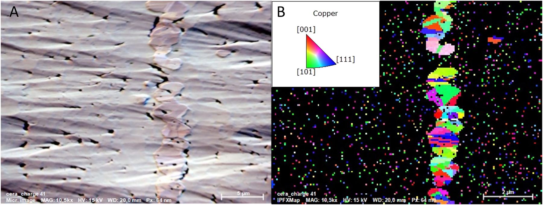
EBSD images of the ion polished battery. (A) Image obtained from backscattered electron detector mounted on the EBSD detector. (B) IPFX map image of Cu grains in the current collector. Inset: Grain orientation.
As observed in the inverse pole figure map in the X-direction (IPFX), the absence of a dominant color suggests no preferred grain orientation, which is further confirmed by the IPF maps in the Y and Z orientations (IPFY, IPFZ in Supplementary Figure S3). This indicates that electron scattering within the Cu layer is enhanced due to grain boundary and dislocation scattering, potentially affecting the electrical conductivity of the current collector at the nanoscale interconnects. However, for a micro-scale battery like CeraCharge, this effect may not be significant enough to impact overall performance.
3.1.3 μCT analysis
Non-destructive 3D imaging of the sample was performed using an μCT system, with the resulting images shown in Figure 4. The multilayered structure of the battery, as discussed earlier, is clearly visible (Figure 4A and ureB). The Cu current collector can be easily distinguished in the μCT images due to its distinct contrast compared to the electrode and electrolyte layers.

μCT images of CeraCharge™ battery. (A) Overview image of ceracharge showing the multiple layers of the battery. (B) Cross sectional image of the battery showing slight misalignment in the Cu layers and the gaps in the Cu layer. (C) 3D planar image showing source of gaps appearing in the SEM images marked by the circle. (D) typical 2D Cu layer with gap areas shown in blue and Cu areas shown in orange.
The cathode and anode Cu current collectors are intertwined, with the overall current being collected at opposite ends of the battery. The thickness determination of the Cu layer is founded on a volume-based local thickness definition and was determined to be 3.8±1.1 μm, which is consistent with the results obtained from SEM and AFM measurements [18]. However, discontinuities in the Cu layer are observed (Figure 4B). While these gaps indicate regions of local discontinuity, they do not represent a complete lateral break in the layer. As shown in Figure 4D, the Cu layer remains uniform, with gaps that account for 20 % of the total area. Although these gaps may significantly hinder electron transport, alternative conductive pathways remain available for electron movement along the plane. Additionally, the presence of isolated Cu islands, which do not contribute to current flow (Supplementary Figure S4), indicates inefficient utilization of the active battery layer. This could lead to localized resistance and suboptimal performance of the battery.
3.2 Elemental and chemical composition analysis
3.2.1 EDX
Figure 5 presents the EDX mapping of the ion-polished battery, enabling material identification. The detector captured characteristic X-rays emitted by excited atoms, generating a spectrum where peaks correspond to specific elements (Supplementary Figure S5). The EDX map highlights element distributions, with vanadium (V) localized in the electrode (cathode/anode) and titanium (Ti) and aluminum (Al) specific to the electrolyte. Phosphorus (P) and oxygen (O) are present in both battery components.

EDX map of ion polished ceracharge battery showing distinct contrast between LATP, LVP and Cu layer. (A) Electron image with slight contrast difference between LATP and LVP. (B) EDX map image revealing the electrode layer through V signal.
As shown in Figure 3A, the electrode layer (3.1 ± 0.6 μm) is thinner than the electrolyte layer (9.6 ± 0.9 μm). While increasing electrode thickness is desirable for higher capacity, reducing the electrolyte thickness too much can lead to short-circuiting issues. Nevertheless, the multilayered structure enhances compaction, improving energy density and enabling a capacity of 0.1 mAh for a compact battery size of 4.4 × 3.0 × 1.1 mm3.
Similarly to SEM images, discontinuities in the Cu layer are also observed in the EDX images. However, as demonstrated in the μCT images (Section 3.1.3), this may not accurately represent the actual structure of the Cu layer.
3.2.2 ToF-SIMS
While EDX provides valuable chemical information, it has limited spatial resolution, typically 1–5 μm, compared to electron imaging and struggles with detecting light elements (Z < 5), such as hydrogen and lithium. Therefore, complementary techniques like ToF-SIMS are necessary for a more comprehensive analysis.
Figure 6 presents elemental mapping obtained from ToF-SIMS measurements, which enable the detection of lithium (Li) signals. The first image was captured using an SESI detector with an FIB gun as the source. It distinctly highlights the contrast differences between the LATP, LVP, and Cu layers, allowing for clear differentiation of these components. As expected, based on chemical composition, Li content is higher in the electrode layer than in the electrolyte layer. A clear distinction between the electrode and electrolyte is evident from the Ti and V signals, while the O signal is evenly distributed, consistent with the expected chemical composition. The phosphorus (P) signal appears weak due to its low secondary ionization yield [19].

ToF-SIMS images of ion polished battery with different elemental composition. Top left image corresponds to imaging using SESI detector with FIB gun as a source.
Notably, the V distribution within the electrode is not uniform, which could negatively impact the electrochemical performance of the cathode or anode. Additionally, the low Cu signal can be attributed to the shallow penetration depth of ToF-SIMS, which analyzes only the top few nanometers of the sample [20]. Furthermore, signal suppression may occur due to the presence of a surrounding nonconductive matrix, such as phosphates.
3.3 Surface and interface-sensitive techniques
3.3.1 AFM analysis
The images of mechanically polished (Figure 7) and ion-polished (Supplementary Figure S6) samples reveal notable differences in surface morphology, phase, and surface potential. The mechanically polished sample exhibits a smoother surface because of filled-in pores, whereas the ion-polished sample appears rougher since the pores are distinguishable and affect the roughness scale (Figure 7A). The pore sizes observed in the height images of the ion-polished sample closely match those seen in SEM images (Figure 2). The presence of pores on the sample surface poses challenges for AFM-based techniques, as these methods rely on precise probe-surface interactions. Deep pores or trenches, a few hundred nanometers in depth, may interfere with accurate phase or surface potential measurements. Compared to mechanical polishing, ion milling produces a more representative cross-section, as it better preserves and reveals the material’s natural pore structure. Nevertheless, the mechanically polished surface offers valuable insights into material distribution. The phase image reflects material contrast, while KPFM images reveal variations in surface potential response under a specific bias. This makes mechanical polishing useful for distinguishing different materials within the sample, despite its higher surface roughness.

AFM images of mechanically polished battery revealing material contrast between LATP, LVP and Cu layers. (A) Height image with filled in pores. (B) NCM phase image with material contrast. (C) KPFM surface potential at 3 V bias with material contrast.
The NCM image (Figure 7B) shows distinct contrast between the LATP, LVP, and Cu layers. LVP layer thickness (3.4±0.5 μm) and LATP layer thickness (10.0±0.8 μm) are comparable to EDX values, while the Cu layer thickness is a bit low (2.4±0.5 μm). Yet, it lies within the standard deviation range of the other measurement techniques. The NCM image of the ion polished sample does not show any difference in the layers (Supplementary Figure S6B). This could be attributed to the ion-polishing step, which reduced surface roughness effects, thereby minimizing variations in the contact area between the AFM tip and the sample surface.
Figure 7C shows the KPFM surface potential at a 3V bias for the mechanically polished sample, highlighting clear contrast between different layers. However, the image of the LVP layer is not an accurate representation, as it is likely distorted. This distortion may have occurred because the ductile nature of Cu allowed it to smear into the LVP layer during the mechanical treatment. To obtain a more accurate representation, ion polishing is necessary in this case. Supplementary Figure S6C presents the KPFM surface potential at a 3V bias, where the Cu layer is distinctly visible. This is expected, as Cu is significantly more conductive than LATP and LVP. The Cu thickness measured from this image (3.1±0.8 μm) aligns well with SEM measurements. The high standard deviation is not due to measurement uncertainty but rather to the rough Cu layer, as also confirmed by XRM observations (Figure 6D).
3.3.2 Raman analysis
Raman spectroscopy was performed at different locations within the multilayered structure (Figure 8). Due to the inhomogeneous nature of the sample, variations in characteristic Raman peaks and their intensities were observed across the different regions, with some peaks appearing only in specific areas. This spectral variation indicates localized chemical and structural differences, making it challenging to distinctly identify individual compounds.
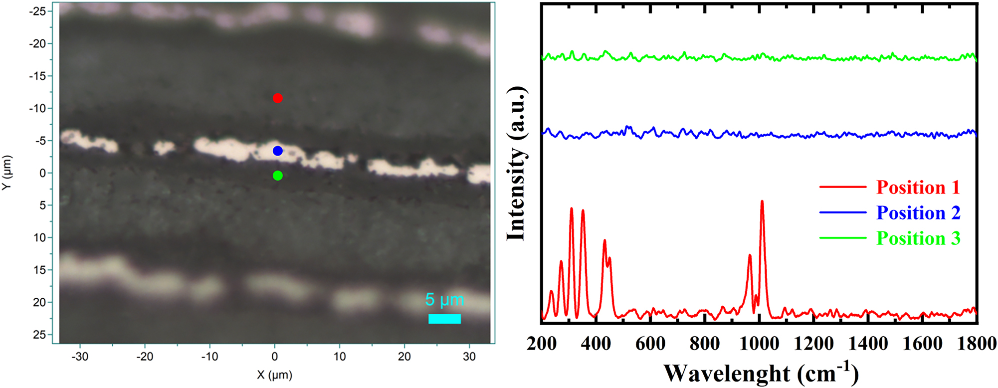
Raman spectra of ion polished battery at three different positions: LATP electrolyte (red), Cu current collector (blue), and LVP electrode (green).
Phosphate groups (PO43−) typically exhibit characteristic Raman bands in the range of 950–1,100 cm−1, corresponding to symmetric and asymmetric stretching vibrations of P–O bonds.
Consequently, the prominent peak around 1,000 cm−1 is likely influenced by phosphate vibrations [10]. Although pure lithium ions are not Raman-active, lithium-containing compounds – such as lithium phosphates or lithium vanadates – can exhibit Raman signatures. Lithium phosphates, in particular, display bands within the 850–1,000 cm−1 range due to P–O stretching modes, which may contribute to or overlap with the peak near 1,000 cm−1.
Vanadium oxides and vanadium phosphates are known to have Raman active vibrational modes, typically with peaks in both the low (200–400 cm−1) and mid-range (near 900–1,000 cm−1) spectral regions [21]. However, the LVP cathode did not show any distinct signals in these ranges. This absence could be attributed to background interference suppressing the signal from the LVP cathode.
As for the Cu layer, no Raman signal was detected, which aligns with expectations, since metallic Cu is Raman-inactive. This is due to the absence of significant changes in the polarizability of the electron cloud during molecular vibrations, a key requirement for Raman scattering.
4 Discussion
4.1 Key findings
In this study, we conducted a comprehensive analysis of an all-solid-state battery (ASSB), specifically the TDK Ceracharge battery, using multiple characterization techniques. To the best of our knowledge, such an extensive investigation of this battery has not been performed before.
Key findings from this study include the observation of porosity in the LATP electrolyte and LVP cathode, as revealed by SEM imaging. These pores, likely formed during sintering or lamination in the fabrication process, can negatively impact battery performance. The multilayer capacitor fabrication method used for this battery inherently introduces some porosity during the sintering and binder burnout stages [22].
Additionally, we found that the LATP layer is relatively thick (∼9.6 μm) compared to LiPON-type microbatteries. This increased thickness is likely intentional to prevent short circuiting between layers, which would otherwise lead to battery failure. Moreover, mechanical polishing led to debris filling the pores, possibly due to fine powder particles or smearing of ductile Cu by diamond polishing disks [23].
Due to the lack of clear contrast between LATP and LVP in SEM images, EDX measurements were employed. By analyzing the vanadium V signal, we determined the thickness of the cathode/anode layer to be ∼3.4 μm. Furthermore, EDX revealed that the gaps observed in the Cu layer were filled with electrode material, meaning these gaps do not necessarily indicate complete loss of electrical connectivity. However, EDX is limited in detecting lithium, necessitating the use of TOF-SIMS.
TOF-SIMS analysis confirmed a higher lithium content in the electrode compared to the electrolyte. The Cu signal appeared weak as TOF-SIMS is highly surface-sensitive (analyzing only a few nanometers in depth), whereas EDX probes deeper (∼1–2 microns) [20].
EBSD analysis of the Cu layer indicated a random grain orientation, with an average grain size between 100 nm and 300 nm, large enough to maintain sufficient electrical conductivity in these thin films [24]. AFM provided additional insights into surface topography, revealing Λ-shaped damage on the ceramic surface caused by ion polishing. This damage is likely due to the angular arrangement of the triple Ar-ion beam guns and high ion beam currents. NCM and KPFM measurements provided valuable insights into the battery components in the mechanically polished samples, despite the rough surface. For the ion-polished sample, while NCM imaging did not offer significant details about the battery components, KPFM effectively differentiated the Cu current collector from the other layers. Future AFM investigations using different modes could provide further insights, particularly in analyzing electrode components at different states of charge [25].
Raman spectroscopy successfully confirmed the presence of the LATP electrolyte. While it does not provide detailed structural insights, its ability to detect key chemical components in a non-destructive manner highlights its potential as an in-line analytical tool for monitoring ASSB manufacturing processes. Given that Raman spectra are highly sensitive to material composition, this technique could serve as an indirect quality control parameter in battery production, allowing for real-time monitoring of electrolyte consistency and potential phase variations. [26].
All the aforementioned measurements required sample preparation, including cutting, grinding, and ion polishing. In contrast, μCT offers a non-destructive method for internal structural analysis. A prior study has discussed the trade-off between imaging volume and resolution in μCT, where high-resolution imaging captures fine details in small volumes, while larger volumes require lower resolution. A deep-learning model was developed to enhance low-resolution μCT datasets, but no detailed characterization of LATP, LVP, and Cu layers was provided in the study [17]. Another non-invasive technique, atomic magnetometry, has demonstrated potential for detecting structural defects, such as cracks caused by thermal damage, within a short time frame [27]. While this method is promising for non-contact battery quality control, it does not provide detailed internal structural information. A key limitation of μCT is the significant time required for high-resolution scans (∼20 h for individual layers). Additionally, only the Cu layer produced a strong signal, while the LATP and LVP layers were not clearly distinguishable.
4.2 Solutions and core challenges
Each method contributes uniquely to the multi-modal investigation of battery materials. SEM and EBSD offer morphological and crystallographic insights, while EDX provides rapid elemental mapping and composition analysis – especially effective when combined with SEM for correlative imaging. AFM/KPFM measures surface potential with nanoscale lateral resolution, useful for distinguishing electrochemical layers. Raman spectroscopy identifies molecular structures and phase distributions, which is particularly valuable for complex cathode composites. µCT supplies a 3D overview of internal features like voids and compaction uniformity in non-destructive fashion. TOF-SIMS, on the other hand, excels at ultra-sensitive elemental and isotopic analysis with nanometer-scale depth profiling. These complementary methods enable a holistic, cross-validated view of battery component structures and interfaces, guiding targeted characterization strategies depending on the research objective and material system (Table 1).
Comparison of characterization techniques used in this study.
| Technique | Spatial resolution | Detection depth | Key information provided | Strengths | Limitations |
|---|---|---|---|---|---|
| SEM | ∼1–10 nm | Surface to ∼1–2 µm | Morphology, contrast, defects | High resolution, easy sample prep | Requires vacuum, limited chemical specificity |
| EBSD | ∼50–100 nm | Top ∼50 nm | Crystallographic orientation, grain boundaries | Reveals microstructure and texture | Needs flat/polished surface, sensitive to prep |
| EDX | ∼1 µm | ∼1–2 µm (material-dependent) | Elemental composition | Fast elemental mapping with SEM integration | Limited to heavier elements, poor light element sensitivity |
| AFM/KPFM | ∼20–100 nm (lateral) | Surface (few nm) | Morphology, surface potential contrast | Sensitive to surface electronic properties | Requires flat, clean surfaces |
| Raman | ∼500 nm | ∼1–5 µm | Molecular bonding, phase identification | Non-destructive, phase-specific | Low spatial resolution, fluorescence interference |
| µCT | ∼1 µm (voxel size) | Bulk (mm to cm) | 3D structure, porosity, internal defects | Non-destructive, large-scale insight | Poor resolution for micro-features |
| TOF-SIMS | ∼100 nm (lateral) | Top few nm (depth profiling possible) | Elemental and isotopic surface composition | Extremely sensitive, capable of depth profiling | Sensitive to matrix effects, sample charging |
High-resolution μCT scanning is inherently time-consuming due to the need for acquiring detailed volumetric data with fine spatial resolution. However, recent technological advancements have significantly mitigated this limitation. Phase-contrast imaging has improved contrast sensitivity, allowing for shorter exposure times without compromising image quality [28], [29]. Furthermore, the adoption of compressed sensing and iterative reconstruction algorithms has accelerated data processing, enabling faster scan completion with preserved resolution [30], [31]. High-speed flat-panel detectors and improved X-ray source brilliance have also contributed to higher throughput and reduced acquisition time [32]. These developments, as discussed in recent literature, are making μCT a more practical and efficient tool for high-resolution battery characterization workflows.
While each characterization technology offers distinct advantages, their application in battery research often presents contradictory challenges, particularly in sample preparation and data integration. Some of the key contradictions are:
Sample Preparation Compatibility: Techniques like ToF-SIMS require ultra-clean, flat surfaces to minimize surface damage, which is often incompatible with techniques like EDX that can tolerate rougher surfaces. This discrepancy becomes a challenge when attempting to use both techniques on the same sample, as each may require different preparation methods.
Data Integration: There are significant challenges when integrating data from surface sensing techniques (such as ToF-SIMS) with bulk phase analysis (such as EDX). ToF-SIMS provides detailed surface information, while EDX offers bulk compositional maps. To reconcile these, co-registration using fiducial markers and AI-driven data fusion frameworks have been proposed as potential solutions to combine data from both techniques accurately [33].
These challenges illustrate the complexity of using complementary techniques on battery samples and highlight the need for more integrated methodologies to overcome incompatibilities and enhance data interpretation.
As solid-state batteries evolve, several core challenges remain unresolved in the characterization of these systems. Key problems include:
Lack of Standardization: Current ASTM and IEC standards do not provide comprehensive protocols for solid-state battery characterization, particularly for evaluating interface stability and mechanical degradation. This gap hinders reliable comparisons between studies and industry adoption.
Cross-Scale Data Fusion: There is no widely accepted methodology for integrating multi-scale data (e.g., microstructural features from μCT and electrochemical behavior from cyclic voltammetry) to obtain a holistic understanding of battery performance. Establishing fusion criteria for such multi-modal data is crucial for advancing the field.
Multi-Modal Integration: The absence of integrated frameworks for combining surface-sensitive techniques like ToF-SIMS with bulk analysis techniques like EDX makes it challenging to derive comprehensive insights into battery performance. Overcoming this issue will be crucial for optimizing solid-state batteries for commercial use.
These unresolved issues call for concerted efforts in standardization, data integration, and methodology development to accelerate the adoption of solid-state batteries in practical applications.
5 Conclusions
This work provides an in-depth, multi-technique characterization of the TDK CeraCharge™ all-solid-state battery (ASSB), offering critical insights into its structural and chemical features. Techniques such as SEM, EDX, Raman spectroscopy, ToF-SIMS, AFM, μCT, EBSD, and plasma-FIB were employed to evaluate both surface and bulk properties. Notably, the observed porosity in the electrolyte and electrodes plays a pivotal role in electrochemical performance, and its visualization highlights the importance of advanced imaging techniques.
While non-destructive tools like μCT enable valuable 3D insights into internal structures, they are constrained by resolution and scan time. Surface-sensitive methods like ToF-SIMS offer high chemical sensitivity but require extremely clean, flat sample surfaces, often incompatible with preparation procedures for bulk techniques like EDX. These incompatibilities underscore the need for improved cross-technique sample preparation protocols. Moreover, integrating datasets from methods with vastly different spatial resolutions and probing depths – such as ToF-SIMS and EDX – remains a challenge. Co-registration methods, the use of fiducial markers, and emerging AI-driven data fusion frameworks are promising approaches to overcome this barrier.
To guide future research, we also provided a comprehensive comparison table outlining the spatial resolution, probing depth, advantages, and limitations of each technique. This framework enables informed method selection depending on the characterization goal – be it surface chemistry, crystallographic mapping, or internal structural analysis.
Ultimately, this work not only contributes to a deeper understanding of failure mechanisms and performance limitations in ASSBs but also establishes a systematic foundation for optimizing analytical workflows and guiding the design of future multiscale characterization strategies.
Funding source: Bundesministerium für Bildung und Forschung
Award Identifier / Grant number: 03XP0520A
Funding source: Bundesministerium für Wirtschaft und Klimaschutz
Award Identifier / Grant number: 16BZF351D
-
Research ethics: Not applicable.
-
Informed consent: Not applicable.
-
Author contributions: All authors have accepted responsibility for the entire content of this manuscript and approved its submission.
-
Use of Large Language Models, AI and Machine Learning Tools: ChatGPT was used to improve the language of the manuscript.
-
Conflict of interest: The authors state no conflict of interest.
-
Research funding: This work was supported by the German Federal Ministry of Education and Research (BMBF) within the research project NaNi-Batt (ID: 03XP0520A) and by the German Federal Ministry for Economic Affairs and Climate Action (BMWK) within the research project 3DPrintBatt (ID: 16BZF351D).
-
Data availability: Not applicable.
References
[1] J. Janek and W. G. Zeier, “Challenges in speeding up solid-state battery development,” Nat. Energy, vol. 8, no. 3, pp. 230–240, 2023, https://doi.org/10.1038/s41560-023-01208-9.Suche in Google Scholar
[2] A. Jetybayeva, A. Umirzakov, B. Uzakbaiuly, Z. Bakenov, and A. Mukanova, “Towards Li–S microbatteries: A perspective review,” J. Power Sources, vol. 573, p. 233158, 2023. https://doi.org/10.1016/j.jpowsour.2023.233158.Suche in Google Scholar
[3] R. Pfenninger, M. Struzik, I. Garbayo, E. Stilp, and J. L. M. Rupp, “A low ride on processing temperature for fast lithium conduction in garnet solid-state battery films,” Nature Energy, vol. 4, no. 6, pp. 475–483, 2019, https://doi.org/10.1038/s41560-019-0384-4.Suche in Google Scholar
[4] N. Tolganbek, A. Mentbayeva, B. Uzakbaiuly, K. Kanamura, and Z. Bakenov, “Li1+xAlxTi2−x (PO4)3, NASICON-type solid electrolyte fabrication with different methods,” Mater. Today: Proc, vol. 25, no. 1, pp. 97–100, 2020. https://doi.org/10.1016/j.matpr.2019.12.279.Suche in Google Scholar
[5] J. Duan, et al.., “Solid electrolyte cracking due to lithium filament growth and concept of mechanical reinforcement – An operando study,” Mater. Today, vol. 70, pp. 33–43, 2023. https://doi.org/10.1016/j.mattod.2023.10.003.Suche in Google Scholar
[6] S. Randau, et al.., “Benchmarking the performance of all-solid-state lithium batteries,” Nature Energy, vol. 5, no. 3, pp. 259–270, 2020, https://doi.org/10.1038/s41560-020-0565-1.Suche in Google Scholar
[7] S. Lobe, A. Bauer, S. Uhlenbruck, and D. Fattakhova-Rohlfing, “Physical vapor deposition in solid-state battery development: From materials to devices,” Adv. Sci. (Weinheim, Baden-Wurttemberg, Germany), vol. 8, no. 11, p. e2002044, 2021, https://doi.org/10.1002/advs.202002044.Suche in Google Scholar PubMed PubMed Central
[8] B. Uzakbaiuly, A. Mukanova, Y. Zhang, and Z. Bakenov, “Physical vapor deposition of cathode materials for all solid-state li ion batteries: A review,” Front. Energy Res., vol. 9, 2021. https://doi.org/10.3389/fenrg.2021.625123.Suche in Google Scholar
[9] N. J. Dudney, “Thin Film Micro-batteries,” Electrochem. Soc. Interf, vol. 17, no. 3, pp. 44–48, 2008, https://doi.org/10.1149/2.f04083if.Suche in Google Scholar
[10] V. Siller, et al.., “High performance LATP thin film electrolytes for all-solid-state microbattery applications,” J. Mater. Chem. A, vol. 9, no. 33, pp. 17760–17769, 2021, https://doi.org/10.1039/D1TA02991F.Suche in Google Scholar
[11] TDK Electronics, “Application Note 2024 – CheraCharge Rechargeable mulilayer ceramic chip”. https://www.tdk-electronics.tdk.com/download/2532510/510b2afefb7a57c791f1552b225c6533/06-dl-application-note.pdf.Suche in Google Scholar
[12] Z. Jian, et al.., “Carbon-coated rhombohedral Li 3 V 2 (PO 4 ) 3 as both cathode and anode materials for lithium-ion batteries: electrochemical performance and lithium storage mechanism,” J. Mater. Chem. A, vol. 2, no. 47, pp. 20231–20236, 2014, https://doi.org/10.1039/C4TA04630G.Suche in Google Scholar
[13] A. Abdigazy, M. S. Islam, M. Arfan, M. F. Hassan, H. Hashemi, and Y. Khan, “A self-orienting single-chip ingestible pill for electrochemical sensing in the GI tract,” in 2024 IEEE Biomedical Circuits and Systems Conference (BioCAS), Xi’an, China, IEEE, 2024, pp. 1–5.10.1109/BioCAS61083.2024.10798307Suche in Google Scholar
[14] E. Perez, C. Augusto-Berlitz, Y. Moursy, S. Oukassi, B. Allard, and G. Pillonnet, “Miniaturized solid-state battery-based DC-DC switched converter,” in 2024 IEEE International Symposium on Circuits and Systems (ISCAS), Singapore, IEEE, 2024, pp. 1–5.10.1109/ISCAS58744.2024.10558604Suche in Google Scholar
[15] K. R. Sadagopan and A. Natarajan, “A 2.4-GHz wideband wireless harvester with integrated autonomous RF input-frequency tracking for FCC-compatible chip-scale battery charging,” IEEE Open J. Solid-State Circuits Soc., vol. 3, pp. 249–261, 2023. https://doi.org/10.1109/OJSSCS.2023.3323913.Suche in Google Scholar
[16] S. Schmickl, T. Faseth, and H. Pretl, “Microwatt power management: challenges of on-chip energy harvesting,” Elektrotech. Inftech., vol. 138, no. 1, pp. 31–36, 2021, https://doi.org/10.1007/s00502-020-00859-w.Suche in Google Scholar
[17] N. S. Johnson, Y. Trenikhina, H. Bale, and S. Kelly, “Deep-learning models enable high-resolution reconstruction of large-volume x-ray microscopy datasets,” in Developments in X-Ray Tomography XV, San Diego, United States, 2024, p. 28. [Online]. Available at: https://www.spiedigitallibrary.org/conference-proceedings-of-spie/13152/3027501/Deep-learning-models-enable-high-resolution-reconstruction-of-large-volume/10.1117/12.3027501.full.10.1117/12.3027501Suche in Google Scholar
[18] T. Hildebrand and P. Rüegsegger, “A new method for the model-independent assessment of thickness in three-dimensional images,” J. Microsc., vol. 185, no. 1, pp. 67–75, 1997, https://doi.org/10.1046/j.1365-2818.1997.1340694.x.Suche in Google Scholar
[19] J. C. Vickerman, D. Briggs, and B. Garrrison, “ToF-SIMS–An Overview,” in ToF-SIMS: Surface analysis by Mass Spectrometry, J. C. Vickerman and D. Briggs, Eds., UK, Surface Spectra/IM Publications, 2001.Suche in Google Scholar
[20] F. Zanderigo, S. Ferrari, G. Queirolo, C. Pello, and M. Borgini, “Quantitative TOF-SIMS analysis of metal contamination on silicon wafers,” Mater. Sci. Eng.: B, vol. 73, no. 1, pp. 173–177, 2000, https://doi.org/10.1016/S0921-5107(99)00456-0.Suche in Google Scholar
[21] L.-L. Zhang, et al.., “Significantly improved electrochemical performance in Li 3 V 2 (PO 4 ) 3/C promoted by SiO 2 coating for lithium-Ion batteries,” J. Phys. Chem. C, vol. 116, no. 23, pp. 12401–12408, 2012, https://doi.org/10.1021/jp301127r.Suche in Google Scholar
[22] A. W. Tavernor, H. -P. S. Li, A. J. Bell, and R. Stevens, “Improved Compaction in Multilayer Capacitor Fabrication,” J. Eur. Ceram. Soc., vol. 19, no. 9, pp. 1691–1695, 1999, https://doi.org/10.1016/S0955-2219(98)00272-6.Suche in Google Scholar
[23] Buehler SumMet, The Sum Of Our Experience: A Guide to Materials Preparation & Analysis: Buehler, 2007. [Online]. Available at: https://www.buehler.com/assets/Catalogues/Downloads/2018_SumMet_Book_Web.pdf.Suche in Google Scholar
[24] T. Sun, et al.., “Dominant role of grain boundary scattering in the resistivity of nanometric Cu films,” Phys. Rev. B, vol. 79, no. 4, 2009, https://doi.org/10.1103/PhysRevB.79.041402.Suche in Google Scholar
[25] A. Jetybayeva, et al.., “Unraveling the state of charge-dependent electronic and ionic structure–property relationships in NCM622 cells by multiscale characterization,” ACS Appl. Energy Mater., vol. 5, no. 2, pp. 1731–1742, 2022, https://doi.org/10.1021/acsaem.1c03173.Suche in Google Scholar
[26] U. Langklotz, M. Schneider, C. Seifert, and A. Michaelis, “Investigation concerning the applicability of raman spectroscopy for prospective inline monitoring of electrode processing for lithium ion batteries,” Mater. Werkst, vol. 42, no. 9, pp. 820–826, 2011, https://doi.org/10.1002/mawe.201100817.Suche in Google Scholar
[27] Y. Hu, et al.., “Rapid online solid-state battery diagnostics with optically pumped magnetometers,” Appl. Sci., vol. 10, no. 21, p. 7864, 2020, https://doi.org/10.3390/app10217864.Suche in Google Scholar
[28] R. Hanke, T. Fuchs, M. Salamon, and S. Zabler, “X-ray microtomography for materials characterization,” in Materials Characterization Using Nondestructive Evaluation Methods, Amsterdam, Elsevier, 2016, pp. 37–74.10.1016/B978-0-08-100040-3.00003-1Suche in Google Scholar
[29] H. T. Reid, Linking Degradation and Safety of Lithium-Ion Batteries, London, UK, University College London Thesis Repository, 2025. Available at: https://discovery.ucl.ac.uk/id/eprint/10203874/.Suche in Google Scholar
[30] L. Wu, L. Zhao, Q. Li, R. Xing, and H. Yao, “Synchrotron radiation data-driven artificial intelligence approaches in materials discovery,” Artif. Intell. Chem., vol. 2, no. 1, p. 100045, 2024. https://doi.org/10.1016/j.aichem.2024.100045.Suche in Google Scholar
[31] S. J. Cooper, S. A. Roberts, Z. Liu, and B. Winiarski, “Kintsugi imaging of battery electrodes: Distinguishing pores from the carbon binder domain using Pt deposition,” J. Electrochem. Soc., vol. 169, no. 7, 2022, https://doi.org/10.1149/1945-7111/ac7a68.Suche in Google Scholar
[32] A. B. Wolbarst and W. R. Hendee, “Evolving and experimental technologies in medical imaging,” Radiology, vol. 238, no. 3, pp. 744–759, 2006, https://doi.org/10.1148/radiol.2381041602.Suche in Google Scholar PubMed
[33] S. Eswara, et al.., “Correlative microscopy combining transmission electron microscopy and secondary ion mass spectrometry: A general review on the state-of-the-art, recent developments, and prospects,” Appl. Phys. Rev., vol. 6, no. 2, 2019, https://doi.org/10.1063/1.5064768.Suche in Google Scholar
Supplementary Material
This article contains supplementary material (https://doi.org/10.1515/mim-2025-0012).
© 2025 the author(s), published by De Gruyter on behalf of Thoss Media
This work is licensed under the Creative Commons Attribution 4.0 International License.