Zn1–xCdxO Microtubes: Synthesis and Optical Properties Using Direct Microwave Irradiation
-
Qusay A. H. Al-Naser

Abstract
Hexagonal Zn1–xCdxO microtubes with CdO contents (x = 0, 1, 3 and 5 %) have been successfully synthesized via direct microwave irradiation. Field emission scanning electron microscopy (FE-SEM), UV–vis spectroscopy, photoluminescence (PL), and energy-dispersive spectrometer (EDS) were employed to characterize the Zn1–xCdxO microtubes. Zn1–xCdxO microtubes have an average diameter of 140 µm, wall thickness of 2~4 µm and length of about 250 µm. UV–vis studies showed that the optical band gap of ZnO microtube (3.27 eV) was reduced to 3.20 eV for Zn0.97Cd0.03O microtube. The PL spectra showed a strong emission peak in the visible region centered at 562.88 nm with a weak UV emission has been detected for Zn0.97Cd0.03O microtube. EDS confirms the presence of Zn and O in ZnO microtube and the absence of Cd as a doping material for CdO-doped ZnO microtubes due to the small amounts of CdO concentration.
Introduction
Nano-microstructured materials exhibit unusual physical and chemical properties significantly different from those of conventional bulk materials, due to its extremely small size or large specific surface area [1, 2]. A large number of investigations have been carried out pertaining to the synthesis and characterization of nano-microstructures of various types/forms for potential application in nano-microdevices. From the material aspect of the nanostructures, the metal oxide nanostructures such as nanowires, nanotubes, and nanobelts have received considerable attention over the past decades, due to their unique electronic, optical, thermal properties and their promising applications in nanoscale devices [3, 4, 5, 6, 7]. Since the report of the ultra-violet (UV) excitonic emission at room temperature, Zinc oxide (ZnO) has attracted enormous interests for its potential optoelectronic applications such as light emitting diode (LE D) and laser diode (LD) in UV or blue spectral region [8, 9, 10]. ZnO has attracted much interest in science and technology due to its versatile properties such as wide, direct band gap of 3.37 eV and a high exciton binding energy of 60 meV at room-temperature [11, 12, 13, 14]. These characteristics find a wide range of applications in optoelectronic and electronic devices [15, 16]. From the industrial point of view, ZnO is considered a very important material because of some advantages such as low production cost, effective nontoxic catalyst, high absorption efficiency of light radiations, and environmental safety [17].
ZnO microtubes exhibit enhanced or novel functionalities due to their higher surface area and the capability of forming composite structures by embedding specific particles in the interiors, and they thus may find potential applications in a wide range of areas, including catalysis, drug delivery, storage and release systems, bio-encapsulation, nano-reactors, and templates for functional architectural composite materials [18, 19, 20].
In order to develop ZnO-based optoelectronic devices, the realization of band gap engineering, i. e. tuning the band gap through doping, is indispensable [21].
Band gap tuning is desirable for wavelength tenability and attaining band gaps corresponding to the visible spectrum. Cadmium oxide (CdO)-doped ZnO would be one of the most promising candidates for narrowing the band gap of ZnO microtubes [22, 23, 24].
Cadmium oxide (CdO) is a II–VI semiconductor, has been widely investigated owing to its potential applications [25, 26]. Pure CdO is a n-type degenerate semiconductor with a simple cubic structure having a direct band gap of 2.2–2.7 eV and two indirect band gaps of 1.18–1.2 eV and 0.8–1.12 eV [27, 28] with higher conductivity (103 Ω−1 cm−1) and transmission (nearly 90 %) [29]. The high transmittance of CdO in visible and near infrared regions of the electromagnetic spectrum along with high carrier mobility and conductivity makes CdO useful for various applications such as solar cells, gas sensors, photo-transistors, diodes, transparent electrodes, liquid crystal displays, IR detectors, and anti reflection coatings [30, 31, 32, 33]. So the controllable synthesis of CdO nanostructures has attracted much attention, and a number of CdO nanostructures have been synthesized in different morphologies including nanowires [34, 35], nanotubes [36, 37], nanofibers [38], nanorods [39, 40, 41, 42] and nanoparticles by different methods, including the template hydrothermal process [43], thermal evaporation method [44, 45], chemical bath deposition method [46] and solvothermal condition [47].
As n-type II–VI semiconductors, hexagonal ZnO and cubic CdO were initially noticed for their potential applications as transparent conducting oxides. Firstly, it was expected that the band gap (3.3 eV) of ZnO can be modulated to 2.3 eV by alloying with CdO, and the luminescence of ZnO-based materials can cover green, blue to UV light spectra [48, 49, 50].
The band gap of Zn1–xCdxO microtubes can be tuned to have luminescence from ultraviolet to blue and green light spectra [51].
In this work, direct heating for microwave processing technology has been used for the synthesis of Zn1–xCdxO microtubes because of its own advantages such as low energy consumption and limits grain coarsening owing to very rapid heating rates and cycles [52, 53]. Thus, microwave heating has a great potential for accelerated kinetics in Zn1–xCdxO microtubes synthesis.
Experimental procedure
The materials used here were commercial ZnO powder, having a purity of 99.9 % and 27 nm particle size, and CdO powder, having a purity of 99.9 % and 50 nm particle size. Zn1–xCdxO (x=0, 1, 3 and 5 %) cylindrical samples of 10 mm diameter were obtained by uniaxial pressing at 3 MPa and followed by annealing at 750 °C for 2 h. The samples were heated in a traveling-wave mode microwave system at 2.45 GHz using susceptor materials as auxiliary heating elements. The details of the traveling-wave mode microwave system have been given in our previous work [54]. Zn1–xCdxO samples were heated at 1,400 °C for 20 min.
The microstructures of the microwave synthesized Zn1–xCdxO samples were observed by field emission scanning electron microscopy (FE-SEM, ULTRA plus, Carl Zeiss, Germany) with an acceleration voltage of 5kV. UV–vis spectrophotometer was used to measure the band gap of the Zn1–xCdxO microtubes. The UV–vis absorption spectra were recorded using (Lambda 750 S/PerkinElmer/USA) UV–vis spectrophotometer in the wavelength region between 330 nm and 700 nm. Optical properties were studied by use of room-temperature photoluminescence (PL) (Horiba Jobin Yvon HR-800 UV setup) measurements. The PL spectrum was measured using a He–Cd laser with the wavelength of 325 nm as the excitation source. Energy dispersive spectroscopy (EDS) was obtained from (X-Max 50; Oxford Instruments; Britain). The samples were coated by carbon before EDS measurement.
Results and discussion
Ternary Zn1–xCdxO (x = 0, 1, 3 and 5 %) microtubes have been successfully synthesized by direct microwave irradiation. The high magnification FE-SEM image shown in Figure 1(a) demonstrated a typical open-ended Zn0.99Cd0.01O microtube of well-defined crystallographic facets and prismatic hexagon shape. Figure 1(b) shows different stages of Zn0.99Cd0.01O microtubes during microwave heating and reveals that the core of Zn0.99Cd0.01O microrods can be selectively removed to form hollow microtubes.

FE-SEM images of the Zn0.99Cd0.01O microtubes synthesized using microwave irradiation: (a) High magnification showing the hexagonal geometric faceted surfaces of the Zn0.99Cd0.01O microtube. (b) Different stages for growth process of the Zn0.99Cd0.01O microtubes.
FE-SEM images of microwave synthesized Zn0.97Cd0.03O and Zn0.95Cd0.05O microtubes were shown in Figure 2.
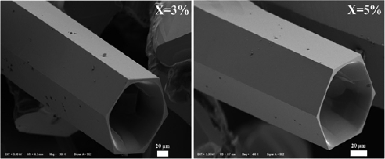
FE-SEM images of the microwave synthesized Zn0.97Cd0.03O and Zn0.95Cd0.05O microtubes.
The average size of the Zn1–xCdxO microtubes is 250 μm in length, 140 μm in diameter and wall thickness of 2~4 µm. The results indicate that the reaction along c-axis is much faster than along other axes. As the vapors of Zn and Cd, the partial pressure of O2, with an approximately uniform distribution around the top and side wall of a ZnxCd1–xO microrod. Thus, symmetric ZnxCd1–xO microtube with well faceted end and side surfaces could be synthesized uniformly.
The analysis of optical absorption spectra is one of the most productive tools for understanding the energy band gap (Eg) of crystalline materials [55]. The energy band gap of the Zn1–xCdxO microtubes can be calculated from the UV–vis light absorbance [56], using the following equation:
where h is plank’s constant, c is the speed of light, and λc is cut-off wavelength [57, 58]. According to eq. (1), the energy band gap of Zn1–xCdxO microtubes of concentrations (x = 0, 1, 3 and 5 %) is (3.27, 3.22, 3.20, and 3.22 eV) respectively.
Figure 3 shows the UV–vis absorption of Zn1–xCdxO microtubes at different concentrations. The band gap of Zn1–xCdxO microtubes decreases in comparison to that of the ZnO microtube.

UV–vis absorption spectra of microwave synthesized Zn1–xCdxO microtubes.
It is observed that the band gaps of Zn1–xCdxO microtubes are narrower than that of pure ZnO microtube due to the influence of CdO doping. Such narrowing in the band gap is associated with an increasing in the carrier concentration to a certain extent to get to the narrower energy gap at a concentration of 3 % of CdO. Band gap narrowing can be explained as a consequence of a change in the nature and strength of the crystalline potential with the addition of CdO impurity dopant ions. So, due to the doping, the band tailing or impurity band becomes broader and finally reaches and merges the bottom of the conduction band causing the decrease of the optical band gap.
Photoluminescence (PL) is a powerful characterization strategy can be utilized to detect the phase composition of the CdO/ZnO system [59]. As shown in Figure 3, the Zn0.97Cd0.03O microtubes has a narrower energy band gap compared to other Zn1–xCdxO (x=1 and 5 %) microtubes. Figure 4 reveals the room-temperature PL spectra comparison between different concentrations of CdO-doped ZnO microtubes under excitation wavelength of 325 nm.

Room temperature PL spectra of Zn1–xCdxO microtubes.
A dominant UV emission band was obtained from ZnO microtube, thus, the UV peak can be attributed to the recombination of free excitons through an exciton-exciton collision process [60]. It is seen that the intensity of UV emission peak decreased with increase of CdO concentration due to decrease in crystallinity with an increase of CdO concentration. This may be attributed to the fact that new defects are introduced after Cd atoms substitute Zn atoms and enter into ZnO lattice due to the electronegativity and ionic radius differences between Zn and Cd. As a result, the bound excitons increase with increase in CdO content, and the near band edge emissions in the UV region decreases [61]. With Zn1–xCdxO microtubes, as number of interstitial Cd (Cdi) defect increases, intensity of blue emission increases due to Cdi and zinc vacancies (Znv) recombination reveals that the increased concentration of CdO enhances the surface defects of Zn1–xCdxO microtubes greatly [62] until the process reaches its optimum value in 3 % CdO and decrease in 5 % CdO which CdO phase probably separates.
It is observed from Figure 4 that Zn0.97Cd0.03O microtube shows poor optical intensity in the near ultraviolet (NUV) region and exhibits a strong increase of intensity in the visible region leading to blue shift of the emission peak from 538.06 nm for ZnO microtube to 562.88 nm which attributed to the high density of the free electrons, which strongly supports that the CdO phase do have evidence effects on the ZnO PL property [63].
To confirm the compositions, Zn1–xCdxO microtubes were subjected to EDS attached to the FE-SEM as shown in Figure 5. The EDS spectra shown in Figure 5(a) confirm the presence of Zn and O in ZnO microtube. The compositions of the elements were shown in the insets. EDS spectrum of Zn0.99Cd0.01O, Zn0.97Cd0.03O, and Zn0.95Cd0.05O microtubes is shown in Figures 5(b), 5(c) and 5(d) respectively, with their composition elements. It is seen the absence of Cd as a doping material which indicates that the Cd substitution did not alter the wurtzite structure of ZnO due to the small amounts of CdO concentration. It is also noted that the concentration of Zn decreases as the doping concentration increases, which very well support the substitution of Cd in Zn site.

EDS pattern of Zn1-xCdxO microtubes: (a) x=0. (b) x=0.01. (c) x=0.03. (d) x=0.05.
Conclusions
Ternary Zn1–xCdxO microtubes with well-defined crystallographic facets and prismatic hexagon shape were successfully synthesized using direct microwave irradiation. The optical properties study indicated that the addition of CdO to ZnO narrowing the band gap of ZnO microtubes. The UV–vis reveals that the optical band gap narrowing from 3.27 eV for ZnO microtube to 3.20 eV for ZnO0.93Cd0.07O microtube. The room-temperature photoluminescence spectra showed a strong emission peak in the visible region centered at 562.88 nm for Zn0.97Cd0.03O microtube compared to that for ZnO microtube, making these tubes have technological importance in optical applications. EDS reveals that the concentration of Zn decreases for ZnO microtube compared to CdO-doped ZnO microtubes while the O increase which very well support the substitution of CdO in ZnO.
Funding statement: This work was supported by the Fundamental Research Funds for the Central Universities (WUT: 2014-IV-061), the Chinese National Science Foundation (51172175, 51072147) and the Hubei Science & Technology Plan (2012FFB05107, 2013BKB006).
References
[1] H. Gleiter, Pest Manag. Sci., 33 (1989) 223–315.10.1016/0079-6425(89)90001-7Search in Google Scholar
[2] J.H. Fendler, Chem. Rev., 87(5) (1987) 877–899.10.1021/cr00081a002Search in Google Scholar
[3] Y. Xia, P. Yang, Y. Sun, Y. Wu, B. Mayers, B. Gates, Y. Yin, F. Kim and H. Yan, Adv. Mater., 15(5) (2003) 353–389.10.1002/adma.200390087Search in Google Scholar
[4] M. Law, J. Goldberger and P. Yang, Annu. Rev. Mater. Res., 34 (2004) 83–122.10.1146/annurev.matsci.34.040203.112300Search in Google Scholar
[5] J.G. Lu, P. Chang and Z. Fan, Mater. Sci. Eng. R, 52(1–3) (2006) 49–91.10.1016/j.mser.2006.04.002Search in Google Scholar
[6] A. Kolmakov and M. Moskovits, Annu. Rev. Mater. Res., 34 (2004) 151–180.10.1146/annurev.matsci.34.040203.112141Search in Google Scholar
[7] Z.L. Wang and J. Song, Science, 312 (2006) 242–246.10.1126/science.1124005Search in Google Scholar
[8] D.M. Bagnall, Y.F. Chen, Zn. Zhu, T. Yao, S. Koyama, My.Y. Shen and T. Goto, Appl. Phys. Lett., 70(17) (1997) 2230–2232.10.1063/1.118824Search in Google Scholar
[9] Z.K. Tang, G.K.L. Wong and P. Yu, Appl. Phys. Lett., 72(25) (1998) 3270–3272.10.1063/1.121620Search in Google Scholar
[10] P. Zu, Z.K. Tang, G.K.L. Wong, M. Kawasaki, A. Ohtomo, H. Koinuma and Y. Segawa, Solid State Commun., 103(8) (1997) 459–463.10.1016/S0038-1098(97)00216-0Search in Google Scholar
[11] M. Chaari, A. Matoussi and Z. Fakhfakh, Mater. Sci. Appl., 2 (2011) 765–770.Search in Google Scholar
[12] H. Usui, J. Phys. Chem. C, 111 (2007) 9060–9065.10.1021/jp071388oSearch in Google Scholar
[13] Y. Cui, C. Wang, G. Liu, H. Yang, S. Wu and T. Wang, Mater. Lett., 65 (2011) 2284–2286.10.1016/j.matlet.2011.04.041Search in Google Scholar
[14] J. Song, Y. Zhang, C. Xu, W. Wu and Z.L. Wang, Nano Lett., 11(7) (2011) 2829–2834.10.1021/nl2011966Search in Google Scholar PubMed
[15] S. Anas, R.V. Mangalaraja, M. Poothayal, S.K. Shukla and S. Ananthakumar, Acta Mater., 55 (2007) 5792–5801.10.1016/j.actamat.2007.06.047Search in Google Scholar
[16] H.S. Kim, F. Lugo, S.J. Pearton, D.P. Norton, Yu.-L. Wang and F. Ren, Appl. Phys. Lett., 92(11) (2008) 112108.10.1063/1.2900711Search in Google Scholar
[17] N. Sangkhaprom, P. Supaphol and V. Pavarajarn, Ceram. Int., 36 (2010) 357–363.10.1016/j.ceramint.2009.09.014Search in Google Scholar
[18] M. Remškar, A. Mrzel, M. Viršek and A. Jesih, Adv. Mater., 19(23) (2007) 4276–4278.10.1002/adma.200701784Search in Google Scholar
[19] H. Lu, L. Liao, J. Li, D. Wang, H. He, Q. Fu, L. Xu and Yu. Tian, J. Phys. Chem. B, 110(46) (2006) 23211–23214.10.1021/jp064079rSearch in Google Scholar PubMed
[20] S.M. Marinakos, M.F. Anderson, J.A. Ryan, L.D. Martin and D.L. Feldheim, J. Phys. Chem. B, 105(37) (2001) 8872–8876.10.1021/jp010820dSearch in Google Scholar
[21] S. Kalusniak, S. Sadofev, J. Puls and F. Henneberger, Laser Photon Rev., 3(3) (2009) 233–242.10.1002/lpor.200810040Search in Google Scholar
[22] T. Makino, Y. Segawa, M. Kawasaki, A. Ohtomo, R. Shiroki, K. Tamura, T. Yasuda and H. Koinuma, Appl. Phys. Lett., 78(9) (2001) 1237–1239.10.1063/1.1350632Search in Google Scholar
[23] T. Makino, C.H. Chia, N.T. Tuan, Y. Segawa, M. Kawasaki, A. Ohtomo, K. Tamura and H. Koinuma, Appl. Phys. Lett., 77(11) (2000) 1632–1634.10.1063/1.1308540Search in Google Scholar
[24] Ü. Özgür, Ya.I. Alivov, C. Liu, A. Teke, M.A. Reshchikov, S. Doğan, V. Avrutin, S.-J. Cho and H. Morkoç, J. Appl. Phys., 98(4) (2005) 041301.10.1063/1.1992666Search in Google Scholar
[25] D.S. Ginley and C. Bright, MRS Bull., 25(8) (2000) 15–18.10.1557/mrs2000.256Search in Google Scholar
[26] F.A. Benko and F.P. Koffyberg, Solid State Commun., 57(12) (1986) 901–903.10.1016/0038-1098(86)90920-8Search in Google Scholar
[27] Z. Zhao1, D.L. Morel and C.S. Ferekides, Thin Solid Films, 413 (2002) 203–211.10.1016/S0040-6090(02)00344-9Search in Google Scholar
[28] Y.-S. Choi, C.-G. Lee and S.M. Cho, Thin Solid Films, 289(1–2) (1996) 153–158.10.1016/S0040-6090(96)08923-7Search in Google Scholar
[29] A.S. Kamble, R.C. Pawar, N.L. Tarwal, L.D. More and P.S. Patil, Mater. Lett., 65 (2011) 1488–1491.10.1016/j.matlet.2011.02.049Search in Google Scholar
[30] B. Saha, S. Das and K.K. Chattopadhyay, Sol. Energy Mater. Sol. Cells, 91 (2007) 1692–1697.10.1016/j.solmat.2007.05.025Search in Google Scholar
[31] L.M. Su, Grote and F. Schmitt, Electron. Lett., 20 (1984) 716–717.10.1049/el:19840490Search in Google Scholar
[32] R. Kondo, H. Okimura and Y. Sakai, Jpn. J. Appl. Phys., 10(11) (1971) 1547–1554.10.1143/JJAP.10.1547Search in Google Scholar
[33] M. Ocampo, A.M. Fernandez and P.J. Sebastian, Semicond. Sci. Technol., 8(5) (1993) 750–751.10.1088/0268-1242/8/5/024Search in Google Scholar
[34] X.Q. Liu, Z.L. Xu, Y.F. Liu and Y.S. Shen, Sens. Actuators B, 52(3) (1998) 270–273.10.1016/S0925-4005(98)00278-0Search in Google Scholar
[35] F. Zhang, F.-Li. Bei, J.-M. Cao and X. Wang, J. Solid State Chem., 181(1) (2008) 143–149.10.1016/j.jssc.2007.11.004Search in Google Scholar
[36] R.R. Salunkhe, D.S. Dhawale, U.M. Patil and C.D. Lokhande, Sens. Actuators B, 136 (2009) 39–44.10.1016/j.snb.2008.10.048Search in Google Scholar
[37] D.H. Fan, J. Cryst. Growth, 311(8) (2009) 2300–2304.10.1016/j.jcrysgro.2009.01.088Search in Google Scholar
[38] A. Askarinejad and A. Morsali, Mater. Lett., 62(3) (2008) 478–482.10.1016/j.matlet.2007.05.082Search in Google Scholar
[39] Bo. Bai, W. Guan, Z. Li and G. Li Puma, Mater. Res. Bull., 46(1) (2011) 26–31.10.1016/j.materresbull.2010.10.002Search in Google Scholar
[40] R. Henríquez, P. Grez, E. Muñoz, E.A. Dalchiele, R.E. Marotti and H. Gómez, Thin Solid Films, 520(1) (2011) 41–46.10.1016/j.tsf.2011.06.030Search in Google Scholar
[41] N.A.M. Barakat, S. Al-Deyab and H.Y. Kim, Mater. Lett., 66(1) (2012) 225–228.10.1016/j.matlet.2011.08.074Search in Google Scholar
[42] T. Ghoshal, S. Kar and S. Chaudhuri, Appl. Surf. Sci., 253(18) (2007) 7578–7584.10.1016/j.apsusc.2007.03.056Search in Google Scholar
[43] H. Zhou, T. Fan and Di. Zhang, Microporous Mesoporous Mater, 100(1–3) (2007) 322–327.10.1016/j.micromeso.2006.11.020Search in Google Scholar
[44] X. Liu, C. Li, S. Han, J. Han and C. Zhou, Appl. Phys. Lett., 82(2) (2003) 1950–1952.10.1063/1.1562331Search in Google Scholar
[45] A.K. Srivastava, S. Pandey, K.N. Sood, S.K. Halder and R. Kishore, Mater. Lett., 62(4–5) (2008) 727–730.10.1016/j.matlet.2007.06.044Search in Google Scholar
[46] D.S. Dhawale, A.M. More, S.S. Latthe, K.Y. Rajpure and C.D. Lokhande, Appl. Surf. Sci., 254(11) (2008) 3269–3273.10.1016/j.apsusc.2007.11.013Search in Google Scholar
[47] Y.C. Zhang and G.L. Wang, Mater. Lett., 62(4–5) (2008) 673–675.10.1016/j.matlet.2007.06.031Search in Google Scholar
[48] A. Ohtomo, M. Kawasaki, T. Koida, K. Masubuchi, H. Koinuma, Y. Sakurai, Y. Yoshida, T. Yasuda and Y. Segawa, Appl. Phys. Lett., 72(19) (1998) 2466–2468.10.1063/1.121384Search in Google Scholar
[49] Y. Jin, B. Zhang, S. Yang, Y. Wang, J. Chen, H. Zhang, C. Huang, C. Cao, H. Cao and R.P.H. Chang, Solid State Commun., 119(6) (2001) 409–413.10.1016/S0038-1098(01)00244-7Search in Google Scholar
[50] D. Zhao, Y. Liu, D. Shen, Y. Lu, J. Zhang and X. Fan, J. Cryst. Growth, 234(2–3) (2002) 427–430.10.1016/S0022-0248(01)01698-0Search in Google Scholar
[51] A. Mohanta and R.K. Thareja, J. Appl. Phys., 103(2) (2008) 024901.10.1063/1.2830985Search in Google Scholar
[52] S. Marinel, E. Savary and M. Gomina, J Microw Power Electromagn Energy, 44(1) (2010) 57–63.10.1080/08327823.2010.11689770Search in Google Scholar
[53] A.W. Fliflet, R.W. Bruce, A.K. Kinkead, R.P. Fischer, D. Lewis, 111,R. Rayne, B. Bender, L.K. Kurihara, G.-M. Chow and P.E. Schoen, IEEE Trans. Plasma Sci., 24(3) (1996) 1041–1049.10.1109/27.533111Search in Google Scholar
[54] Q.A.H. Al-Naser, J. Zhou, H. Wang, G. Liu and L. Wang, Mater. Res. Bull., 66 (2015) 65–70.10.1016/j.materresbull.2015.01.037Search in Google Scholar
[55] S. Gowrishankar, L. Balakrishnan and N. Gopalakrishnan, Ceram. Int., 40 (2014) 2135–2142.10.1016/j.ceramint.2013.07.130Search in Google Scholar
[56] J. Von Behren, M. Wolkin-Vakrat, J. Jorne and P.M. Fauchet, J. Porous Mater., 7 (2000) 81–84.10.1023/A:1009663210016Search in Google Scholar
[57] P.S. Hale, L.M. Maddox, J.G. Shapter, N.H. Voelcker, M.J. Ford and E.R. Waclawik, J. Chem. Educ., 82(5) (2005) 775–778.10.1021/ed082p775Search in Google Scholar
[58] L. Kumari and W.Z. Li, Cryst. Res. Technol., 45(3) (2010) 311–315.10.1002/crat.200900600Search in Google Scholar
[59] V. Venkatachalapathy, A. Galeckas, M. Trunk, T. Zhang, A. Azarov and A. Yu, Kuznetsov, Phys. Rev. B: Condens. Matter Mater. Phys., 83(12) (2011) 125315.10.1103/PhysRevB.83.125315Search in Google Scholar
[60] S.C. Lyu, Ye. Zhang, H. Ruh, H.-J. Lee, H.-W. Shim, E.-K. Suh and C.J. Lee, Chem. Phys. Lett., 363 (2002) 134–138.10.1016/S0009-2614(02)01145-4Search in Google Scholar
[61] A.A. Dakhel, Opt. Mater., 31 (2009) 691–695.10.1016/j.optmat.2008.08.001Search in Google Scholar
[62] M.V. Vaishampayan, I.S. Mulla and S.S. Joshi, Mater. Res. Bull., 46 (2011) 771–778.10.1016/j.materresbull.2010.11.007Search in Google Scholar
[63] K. Tanaka, A. Kunioka and Y. Sakai, Jpn. J. Appl. Phys., 8(6) (1969) 681–691.10.1143/JJAP.8.681Search in Google Scholar
© 2017 Walter de Gruyter GmbH, Berlin/Boston
This article is distributed under the terms of the Creative Commons Attribution Non-Commercial License, which permits unrestricted non-commercial use, distribution, and reproduction in any medium, provided the original work is properly cited.
Articles in the same Issue
- Frontmatter
- Research Articles
- Calculation of the Spontaneous Polarization and the Dielectric Constant for the Ferroelectric N(CH3)4HSO4 Using the Mean Field Model
- Structural Properties of Molten CaO–SiO2–P2O5–FeO System
- Direct Acid Leaching of Vanadium from Stone Coal
- Effects of Cu Distribution on Solidification Microstructure in Transition Layer of Cu/Al Composite Ingot Prepared by Casting Aluminum Method
- Plasma Methods of Obtainment of Multifunctional Composite Materials, Dispersion-Hardened by Nanoparticles
- Microstructure and Diffusion Behaviors of the Diffusion Bonded Mg/Al Joint
- Phosphorus Segregation in Meta-Rapidly Solidified Carbon Steels
- Effects of Temperature and Strain Rate on Tensile Deformation Behavior of 9Cr-0.5Mo-1.8W-VNb Ferritic Heat-Resistant Steel
- Zn1–xCdxO Microtubes: Synthesis and Optical Properties Using Direct Microwave Irradiation
- Oxidation Kinetics and Spallation Model of Oxide Scale during Cooling Process of Low Carbon Microalloyed Steel
- Effect of Cr2O3 Pickup on Dissolution of Lime in Converter Slag