Light sources for high-volume manufacturing EUV lithography: technology, performance, and power scaling
-
Igor Fomenkov
Igor Fomenkov is an ASML Fellow in Technology Development Group in San Diego, California. After completing a PhD in Physics and Mathematics at Moscow Institute of Physics and Technology (MPTI) in 1986, he joined General Physics Institute as a senior scientist, where he worked in the field of interaction of high intensity laser radiation with matter and diagnostics of laser produced plasma. He joined Cymer in 1992 and worked on the development of high power, high reliability KrF and ArF Excimer lasers for DUV (at 248 nm and 193 nm) microlithography. Since 1997 he has been conducting research and development of sources for Extreme Ultraviolet Lithography at 13.5 nm. Over several years of research on EUV light generation, based on Discharge Produced Plasma and Laser Produced Plasma, he has been involved in defining the source architecture, namely Laser Produced Plasma EUV source using high power, high repetition rate CO2 laser and tin droplets as source target material and development of the source for High Volume Manufacturing. He was appointed Cymer Fellow in 2003 and ASML Fellow in 2014. He has authored over 50 technical papers in the field of Laser Produced Plasma, DUV lasers and sources for EUV lithography, and holds over 100 patents in the areas of DUV and EUV light sources.
 ,
David Brandt
,
David Brandt
Alexander Schafgans is a principal scientist at Cymer/ASML, the global leader in developing light sources used by the semiconductor industry to pattern advanced logic and memory. In his role at Cymer, Schafgans has been focused on leading EUV power scaling activities from 10 W through 500 W. During his PhD in Physics, Schafgans focused on the infrared and optical properties of correlated electron materials and graduated from UC San Diego in 2011.
Slava Rokitski is a Senior Manager of System Design at Cymer, an ASML company. He received a PhD degree in electrical engineering at the University of California, San Diego, where he performed research on real-time ultrafast optical information processing and detection. At Cymer Slava has been developing technologies for 193 nm and 248 nm high power excimer laser systems for DUV lithography. Most recently Slava has been developing technologies for high power CO2 master-oscillator-power-amplifier laser systems, used in laser produced plasma extreme ultraviolet light sources.
Michael Purvis serves as the Systems Power Architect for the EUV Source Program at ASML San Diego. Over the last decade, Michael has published in the field of laser created plasmas. His initial investigations at Colorado State University included developing discharge and laser produced EUV lasers for applications in plasma diagnostics, after which he worked on theoretical plasma modelling and high energy density experiments at CSU, Lawrence Livermore National Labs and SLAC. He is now applying his experience with plasmas generated in the femtosecond to nanosecond time scales towards the development of EUV light sources at ASML.
Silvia De Dea received her PhD in Chemical Engineering from The University of California, San Diego in 2008. Her research interests include novel nanomaterials and analytical instruments, materials development for extreme conditions and EUV light technology. She has been with Cymer (now ASML) since 2008 focusing on technology development of EUV sources for semiconductor lithography. She is a Principal Scientist with ASML working on EUV optics lifetime and materials performance.
Jayson Stewart received his PhD in Physics from the University of Colorado in 2009. His research interests focus on light-matter interactions and EUV light source development. In 2012, Jayson joined the ASML team as a research scientist to work on the EUV light source within the technology development group. His work focuses on managing the debris resulting from the laser produced plasma.
Matthew Graham received his PhD in Mechanical Engineering from University of California San Diego in 2007. In 2008 he joined Cymer/ASML working on the DUV light source control system and in 2009 transitioned to development of the EUV light sources for semiconductor lithography. He is currently a Staff Engineer working on control systems around the plasma generation process in the EUV light source.
Daniel J. Riggs has a BS in Mechanical Engineering, a BA in Mathematics: Applied Science, and an MS and PhD in Engineering Science, all from the University of California, San Diego (UCSD). He has worked as a control systems engineer at Cymer since 2006. For the first several years, his focus was high performance control system development for Cymer’s DUV laser products. Since 2009, his focus has been EUV system and control system architecture and design.
Daniel Brown currently serves as Vice President of Technology Development for ASML San Diego. In this role since 2010, he previously held the positions of Vice President, Technology Development and Vice President, Engineering within the Deep-Ultraviolet Product Group in Cymer, Inc. In his current role, he is chartered with overseeing the technology activities for the company’s EUV light source development and deep-ultraviolet light source products to meet the demands of the semiconductor marketplace. Prior to joining Cymer in 2000, Brown a served for over 11 years in various Australian Research Council Fellow positions at Macquarie University (located in Sydney, Australia) including Australian Senior Research Fellow and Australian Research Fellow, responsible for development of novel high-power ultraviolet laser sources based on nonlinear frequency conversion of high-pulse-rate laser systems. Dr. Brown holds a Doctorate degree in physics and a Bachelor’s degree in science from the University of New England in Australia.

Abstract
Extreme ultraviolet (EUV) lithography is expected to succeed in 193-nm immersion multi-patterning technology for sub-10-nm critical layer patterning. In order to be successful, EUV lithography has to demonstrate that it can satisfy the industry requirements in the following critical areas: power, dose stability, etendue, spectral content, and lifetime. Currently, development of second-generation laser-produced plasma (LPP) light sources for the ASML’s NXE:3300B EUV scanner is complete, and first units are installed and operational at chipmaker customers. We describe different aspects and performance characteristics of the sources, dose stability results, power scaling, and availability data for EUV sources and also report new development results.
1 Introduction
Extreme ultraviolet (EUV) lithography is expected to succeed in 193-nm immersion multi-patterning technology for sub-10-nm critical layer patterning. In order to be successful, EUV lithography has to demonstrate that it can satisfy the industry requirements in the following critical areas: power, dose stability, etendue, spectral content, and lifetime. Currently, development of second-generation laser-produced plasma (LPP) light sources for the ASML’s NXE:3300B EUV scanner is complete, and first units are installed and operational at chipmaker customers.
EUV lithography research began in the late 1980s, and by early 1990s, the first successful results have been published [1]. At this time, the main concepts considered for EUV light generation were based on laser-produced plasma [2]. Several more concepts for EUV light generation, including various types of electrical discharge-produced plasma, were proposed [3]. An overview of the further development of EUV sources toward high-volume manufacturing (HVM) [4] and technology aspects of EUV power extendibility [5] was also discussed. Different aspects and performance characteristics of the sources utilizing high-power CO2 laser and Sn droplet target as well as related research and development progress were described in detail in several earlier publications [6], [7], [8], [9], [10], [11]. We described initial dose stability results, power scaling, and availability data for ASML’s 3100 first-generation sources [12], [13] and also reported several new development results [14], [15], [16]. Ten first-generation NXE:3100 sources have been operational for over 5 years; five systems were deployed to customers for use in process development at early adopters of EUV lithography technology. The key features of the NXE platform and the scanner performance during system introduction were reviewed in detail [17]. In this paper, we report on the recent progress in satisfying the main industry requirements for high-volume adoption of EUV technology.
The schematic diagram of an EUV source is shown in Figure 1. The LPP source is comprised of a few main components: (i) a high-power CO2 laser consisting of a master oscillator and power amplifiers (MOPA), (ii) a beam transport system (BTS) including the focusing and beam position control, (iii) a vacuum vessel that houses a droplet generator, collector, and metrology modules. The CO2 laser light is focused onto a Sn droplet delivered by the droplet generator. The laser-plasma interaction takes place at the primary focus of the ellipsoidal collector mirror. The laser-droplet alignment is measured with optical metrology modules and sensors providing feedback to maintain synchronization and optimal performance. The ellipsoidal mirror transmits EUV light collected from the plasma and redirects it through the intermediate focus aperture into the illumination optics of the scanner [14], [15], [16]. Figure 2 shows the ASML NXE:3300B source with the source and the laser systems connected with a beam transport system.
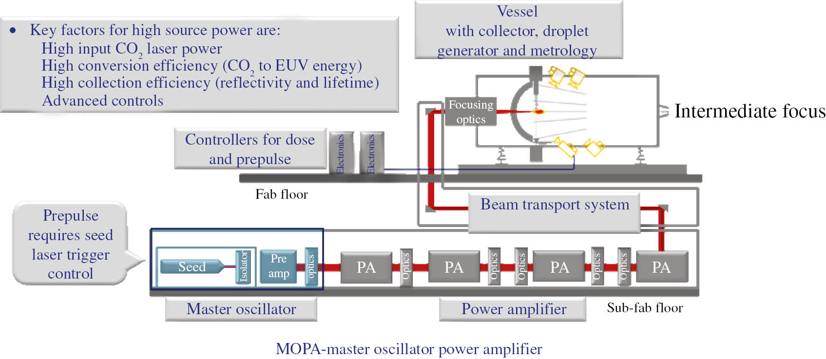
Schematic of LPP source system.
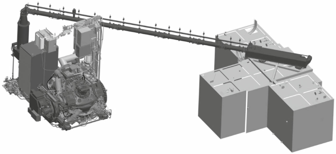
Scale drawing of a laser-produced plasma source for ASML NXE:3300B.
To be used in EUV lithography, the source needs to meet specifications for the following parameters: (i) power, (ii) spectral content, (iii) etendue, (iv) dose stability, and (v) lifetime. These parameters are closely coupled and should be carefully considered when engineering the source. Source power is arguably the most important requirement. The power specification has evolved over the years and is driven by the need of lithography systems to print at a higher resolution and an ever-increasing throughput.
The leading edge manufacturers of integrated semiconductor electronics have continued to make tremendous progress at packing more devices onto their chips using 193-nm immersion lithography by introducing double- and quadruple-patterning techniques. Device manufacturers currently project that EUV lithography will be used in HVM at the 7-nm node and beyond. In the meantime, the throughput required from lithography exposure tools has continued to climb, leading to EUV source power requirements of ~200 W at the introduction to HVM [18].
Controlling source debris is also an extremely important aspect of the LPP source design. Early in the development of LPP sources for lithography, it was realized that the total mass of target material used during the laser-plasma interaction would need to be minimized to avoid unnecessary generation of debris in the form of target fragments, clusters of neutrals and ions that do not contribute to the EUV emission. Several designs aiming to limit the mass of the target exposed to the high-irradiance laser pulse have been conceived and tested over the years. Starting from a solid surface (e.g. rotating cylindrical target to provide a fresh surface for every laser pulse), to thin target tapes, spray jets, liquid filaments, and finally to small droplets, the amount of fuel material that could be ablated by the laser pulse and ends up as debris was reduced dramatically [3]. Even now, considerable effort is going into reducing the size of the droplet, control of the precise spatial and temporal characteristics of the target, and increasing the target material supply to ensure that droplet generator lifetime (or runtime) is not a limiting component in the overall throughput of the EUV scanner.
2 HVM EUV source requirements
2.1 Power
The key challenge of EUV lithography is achieving sufficiently high wafer throughput. EUV mirrors typically have a reflectivity of less than 70%, which leads to very high requirements for the power of the EUV light source to overcome the high losses. To achieve a throughput of 100 wafers per hour (WPH) at a typical scanner duty cycle of 60%, the power at the wafer should be greater than about 550 mW, which means that the EUV source power provided to the exposure tool at intermediate focus should be greater than 200 W or 10 Wcm2/mJ as shown in Figure 3 [19]. For comparison, current 193-nm light sources for lithography have power levels of 90 W to support a throughput of 200 WPH [20].
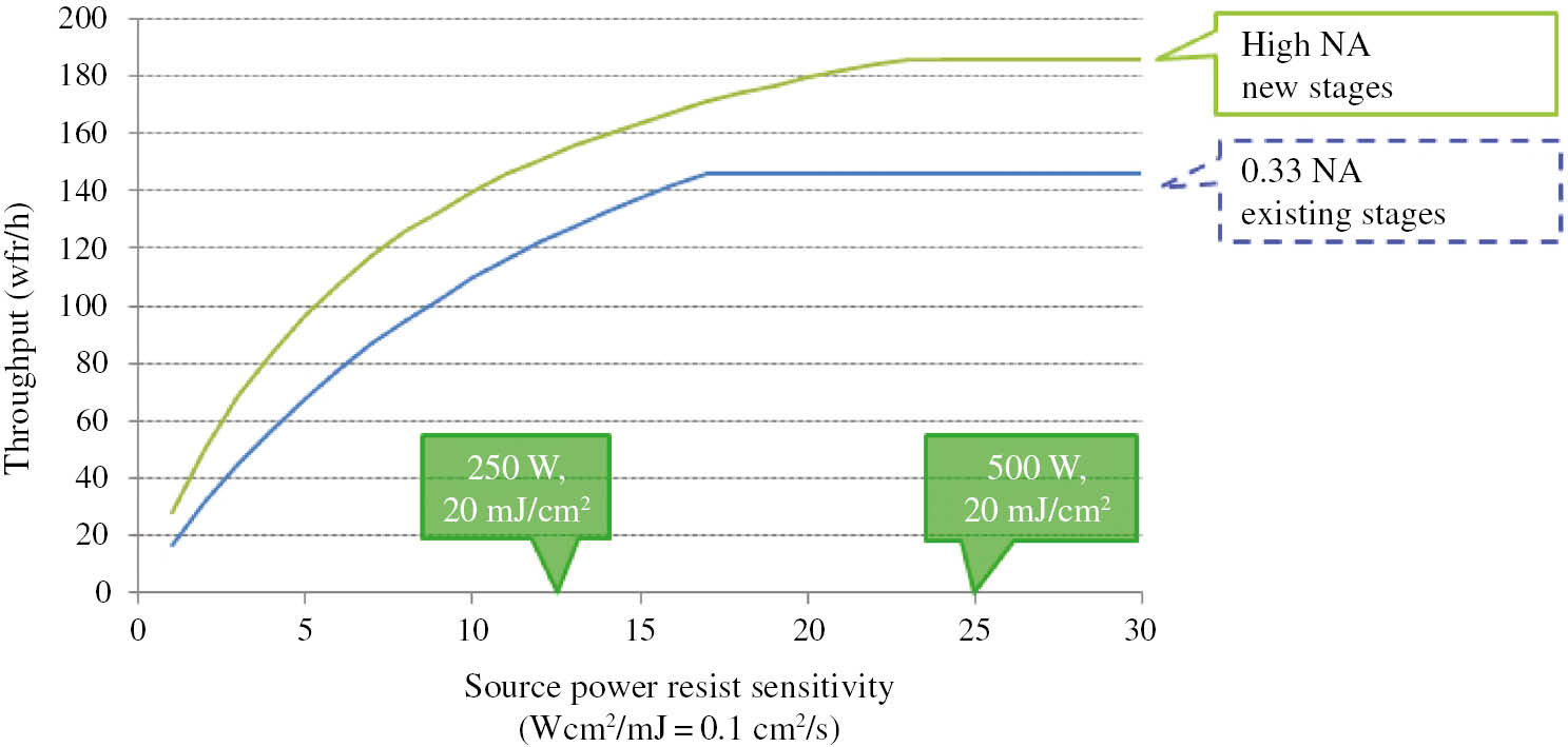
Typical wafer throughput model used to estimate source power requirements.
To produce this level of EUV, power for the scanner plasma is produced using a high-power laser beam focused on Sn droplets with average conversion efficiency from laser pulse energy to EUV pulse energy of approximately 5% [21]. After the loss due to the efficiency of collecting the plasma light (collection solid angle) and the transmission of the background gas within the source, more than 20 kW of laser power is needed to produce 200 W of EUV power at the intermediate focus.
2.2 Spectral content
The EUV scanner uses many reflective surfaces utilizing Mo/Si multilayer films. For this reason, the source spectrum needs to be centered at 13.5 nm within a bandwidth of 2%, as shown in Figure 4 [7], [8]. Even in this case, the light transmission is quite ineffective. For example, in the scanner with 10 reflections from intermediate focus (IF) to the wafer and peak mirror reflectivity of 67%, the overall transmission is about 2%.
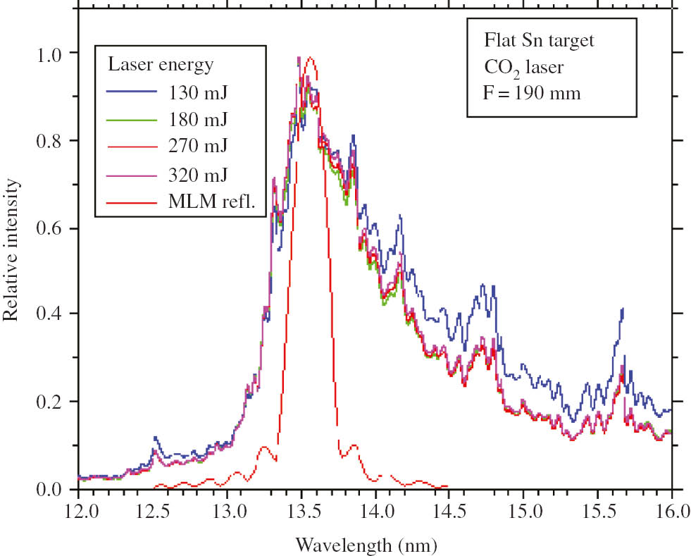
In-band EUV spectrum is well matched with the Mo/Si MLM reflectivity.
The EUV source also has to be spectrally pure, limiting the amount of light in the DUV/UV range (130 nm–400 nm) as well as IR range (mainly at the wavelength of the drive laser). This is because the light at these wavelengths can also be transmitted by the scanner optics and cause undesirable photoresist exposure or excessive thermal loads.
2.3 Etendue
The source etendue is important for matching to the EUV scanner. It is defined as the product of the area of the EUV-emitting plasma and the solid angle subtended by the collector optics. The specification is generally accepted to be less than 1–3.3 mm2 sr and depends on the optical design of the illuminator and projection optics [3]. If the etendue of the source is too large, not all of the light can be coupled to the optical system of the scanner.
2.4 Dose stability and control
Process control in lithography relies on the ability to control the energy delivered to the wafer to expose the resist. For critical features, the exposure latitude is on the order of only a few percent. To achieve sufficient control, the source, itself, should contribute a fraction of a percent of the dose error. In a pulsed-source operation, this stability can be achieved with a high-repetition rate and strict pulse-to-pulse energy control. Current LPP sources operate at a repetition rate of 50 kHz and are capable of <0.5% dose error [22].
2.5 Lifetime
Another very important characteristic of the EUV source is its lifetime. It is critical in terms of cost-of-ownership and the economic viability of EUV lithography. Early on, a target of 30000 h was set for the most critical components of the source. For LPP sources, the collector is arguably the most critical component in terms of lifetime due to the harsh environment in which it resides and the cost of a large curved hyper-smooth multilayer-coated EUV optic. Tin debris, high-energy ions, and neutrals from the plasma can interact with the collector surface and have the potential to degrade its reflectivity over time.
3 Laser-produced plasma source system
ASML NXE systems use CO2 laser with multiple stages of amplification to reach the required power level of >20 kW. It may be operated in pulsed mode at ~50 kHz with radiofrequency (RF) pumping from generators operating in the MHz range. The laser is typically installed in the sub-fab along with its RF generators and water-to-water heat exchangers. The source controller may turn on and off bursts of pulses for exposing a 26×33-mm field sizes. The ratio of time when the burst is on to the burst period defines the duty cycle. As the source power is increased, the time to scan a full field decreases, making the overhead time to step between fields a more significant part of the overall throughput budget.
The beam may be expanded as it leaves the drive laser to maintain the energy density on the BTS mirrors within a certain operating range. Turning mirrors may be used to allow the beam to travel from the sub-fab to the fab through the waffle-slab floor with the needed flexibility for positioning the laser with respect to the source vessel (and scanner) on the floor above. The laser and BTS are typically completely enclosed and interlocked to meet laser class 1 requirements. The BTS delivers the beam to a focusing optical system where the 10.6-μm wavelength light is focused to a minimum spot size. The focused beam propagates through a central aperture in the collector and strikes the droplet at the primary focus of the ellipsoidal collector mirror inside the vacuum space of the source vessel chamber.
The droplet generator delivers liquid tin droplets of, for example, ~30-μm diameter to the same position at 50-kHz repetition rate; both laser pulse and droplets are steered and timed to ensure proper targeting. The laser pulse vaporizes and heats the tin into a plasma cloud. The EUV light emitted by the plasma may be collected and transmitted with a multilayer-coated ellipsoidal mirror to an IF where it passes through a small aperture into the scanner volume that houses the illumination optics. Other modules on the source vessel may include some metrology modules for measuring EUV energy and for imaging of droplets and plasma.
4 EUV power scaling
With the advent of MOPA pre-pulse technology, significant progress has been made to produce higher EUV power levels required for HVM. EUV power at intermediate focus on the order of ~200 W has been demonstrated [18]. The development of higher-power CO2 lasers, together with higher conversion efficiency achieved through improved laser-plasma energy coupling, has resulted in an order-of-magnitude increase in EUV power at IF over the past few years. Here, we describe some recent developments, as well as provide some insight into the motivation behind historical architectural changes and future improvements.
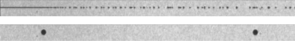
The architecture of a high-power CO2 laser is of great importance for successfully scaling the EUV power emitted by the laser-produced plasma as it is determined how the EUV-generated plasma is produced. Historically, three different drive laser architectures and the methods for producing EUV plasma have been employed. They are commonly referred to as NOMO (no master oscillator), master oscillator, power amplifier (MOPA), and MOPA with pre-pulse. NOMO is a technique for producing plasma whereby a grating or a mirror is placed on the backside of the laser gain medium [23]. As the tin droplet travels through the focal region, it serves as a mirror to complete the laser cavity. Ideally, the total stored laser energy is delivered only once the droplet has entered the focusing volume. The advantages of this architecture include its simplicity and precise laser-to-droplet timing without any droplet detection or control because it is an inherently self-timed and stable system. This was the principle of operation for NXE:3100 light sources installed at customer sites starting in late 2010 (Figure 5). These light sources produced up to 10 W of dose-controlled EUV power at multiple customer sites by 2011 [12], [13]. In this configuration, the lasers were producing roughly 8 kW of power on-droplet (laser energy intercepted by the tin droplets that can be converted into EUV), with an average CE of ~0.8% and dose overhead near 45%. This technology allowed chipmakers to start manufacturing process development of devices utilizing EUV patterning approximately 5–7 years before HVM tools became available.
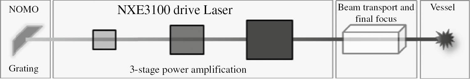
Schematic of the NOMO technique, where a grating is mated with three-stage power amplifiers. As the Sn droplet crosses through the laser focus, the laser gain is rapidly dumped, resulting in plasma formation.
When considering how to scale EUV power from 10 W, it is clear that both laser power and CE must be greatly increased from the NXE:3100 NOMO values. There are two primary drawbacks with the NOMO architecture for EUV power scaling. First, the amount of stored energy in the laser is limited by parasitic reflections, which results in amplified spontaneous emission, thereby, depleting the gain available for making plasma and limiting the total laser power. Second, as the NOMO laser pulse is dependent upon stochastic processes between the droplet and the laser gain medium, the precise laser pulse shape cannot be controlled, placing limits on CE [23]. Therefore, NOMO has EUV scaling limitations that must be overcome with architectural solutions.
Following the development of the NOMO technique, the architecture transitioned to seeded laser amplifier techniques, namely, MOPA and MOPA with pre-pulse (Figure 6). Both techniques involve a master oscillator, which generates a laser pulse that seeds the power amplifiers for single-pass gain extraction. The seed pulse is temporally triggered by the tin droplet such that the laser pulse and the tin droplet arrive at the primary focus at precisely the same instant. The MOPA pulse generation and shaping componentry are all included in the seed system module, which was first mated with the NXE:3100 three-stage power amplifier system for research and development throughout 2011 and 2012. By pairing the laser power amplifiers with the MOPA architecture, it was possible to greatly increase the laser power and demonstrate 30 W of EUV meeting dose specifications. Yet, without pre-pulse, the NXE:3100 MOPA architecture demonstrated relatively low CE of ~1% [23].
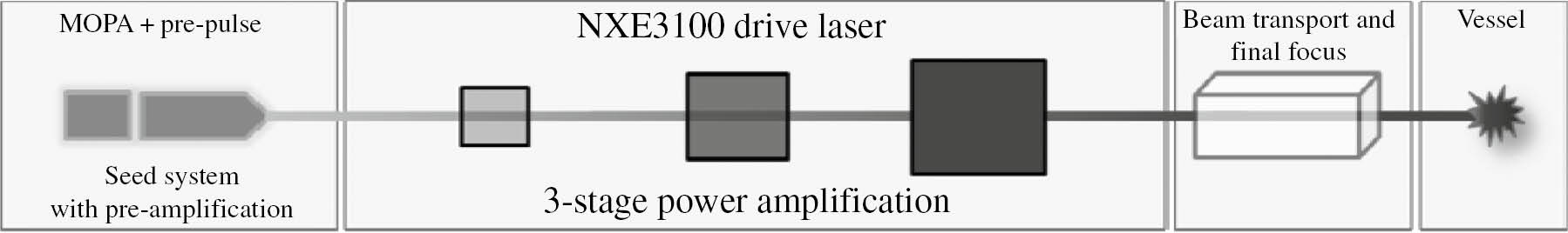
Schematic of the NXE:3100 MOPA pre-pulse architecture.
With the addition of pre-pulse technology to the MOPA architecture, CE can be significantly increased. The pre-pulse is a laser pulse which impacts the droplet prior to the main pulse, transforming the droplet into an improved target for enhanced plasma formation. The pre-pulse modifies the initial droplet into a larger target, resulting in increased surface area and more favorable density, demonstrating the importance of precisely controlling the material distribution for better laser energy coupling. Figure 7 illustrates that pre-pulse is one of the key EUV power scaling approaches employed to date, showing the relationship between CE and target size as generated by the pre-pulse.
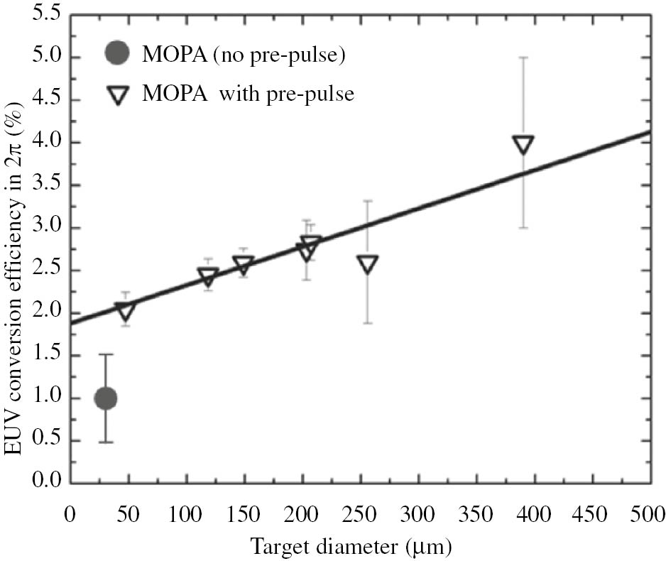
Conversion efficiency as a function of target diameter formed by the pre-pulse. All data were collected on an NXE:3100 MOPA pre-pulse stand-alone source. Vertical bars show standard deviation of 1500 sequential pulses.
By 2013, the NXE:3100 MOPA pre-pulse systems under development were capable of 50 W of EUV power while meeting dose specifications with ~30% overhead [23]. With the architectural improvements over the NOMO technique, the drive laser was capable of ~12 kW of on-droplet power with ~2.5% CE. However, there were two issues with the NXE:3100 MOPA pre-pulse development systems for EUV power scaling: sub-optimal thermal performance of transmissive focusing optics at higher laser powers and insufficient available laser power in the three-stage power amplification chain. In order to address these drawbacks and deliver higher EUV power to customers, the NXE:3300 MOPA pre-pulse architecture was developed. In addition to the pre-pulse capability, an additional power amplification stage was added, thereby, increasing the available laser power, while the focusing optics were changed to an all-reflective design to enable better thermal performance.
The first NXE:3300 systems were operational by mid-2014 and produced >40 W of dose-controlled EUV power with the MOPA pre-pulse technique [23], which was later increased to 80 W and then to 100 W of dose-controlled EUV power at multiple locations including customer sites [23].
To scale beyond 100 W, the development of a high-power seed system (HPSS) was initiated. The architecture has to provide better pulse-shaping capability, greater pre-amplification, and improved isolation from parasitic effects. As part of the development activities, and to clearly assess the performance enhancements offered by the HPSS, a breadboard HPSS was mated with a standard NXE:3100 three-stage amplification chain. Because the HPSS has greater pre-amplification, it can more deeply saturate the power amplifiers, which results in many benefits. One of these benefits is the increase in the peak instantaneous power of the laser pulse at the exit of the amplification chain. Indeed, the HPSS delivered ~4% CE in this configuration [23]. Therefore, not only does the HPSS enable the laser power to be increased but also provides an increase in CE.
Similar to the breadboard development approach employed with the HPSS, the first high-power drive lasers (HPDLs) were built utilizing four-stage power amplifiers. The HPDL also uses more powerful amplifiers that, in factory acceptance tests qualifying the new architecture, achieve ~30 kW when coupled with a standard seed system (~25% increase over the standard NXE:3300 drive laser under the same conditions) [23].
In 2015, performance of fully integrated HPSS with HPDL was successfully demonstrated on in-house research platforms operating at typical customer conditions. With regard to the instantaneous laser power, the HPDL together with a HPSS produces laser pulses that are roughly 2–3× higher peak power than an NXE:3300 laser system. Such improvements in the main pulse characteristics, in addition to target formation developments, have enabled access to even more favorable plasma conditions, leading to mean CE in excess of 5% [24]. By late 2015 and early 2016, a modified NXE:3300B source with HPSS and HPDL had demonstrated 1 h of dose-controlled EUV power at 210 W, illustrating the ability for LPP EUV source technology to meet HVM needs. These results are shown in Figure 8 and represent the highest dose-controlled EUV source power at full duty cycle reported, to date. Figure 9 places the recent demonstrations of >200 W dose-controlled performance in the context of the historical EUV power scaling. Progress on power scaling has continued since early 2016 in-line with this historical trend.
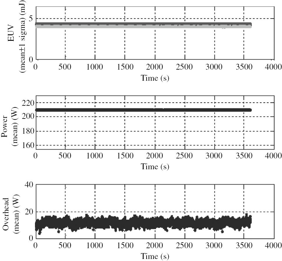
Stable operation of the ASML-Cymer LPP source at 210 W for 1 h.
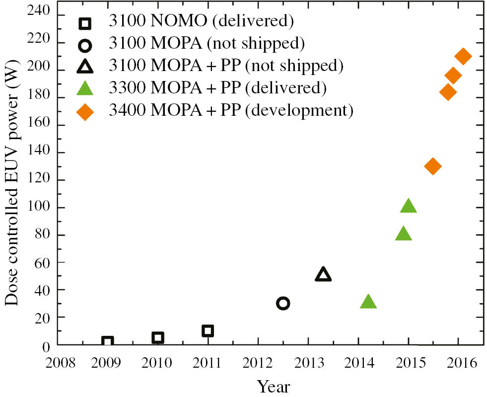
Historical EUV power scaling trend using LPP sources. All data points show the delivered, dose-controlled EUV power at IF and must meet dose specifications for energy stability at the wafer level for at least 1 h to qualify for representation on this plot.
5 Tin target delivery
One of the key technologies of an EUV LPP source consists in the generation of extremely small and stable tin (Sn) droplets at high frequency, which are used as the fuel for producing the plasma and EUV light. The droplet generator provides a constant stream of liquid tin droplets to the focal point of the collector where the CO2 laser pulse is used to create the light-emitting plasma. The main requirement for the droplet generators is to deliver small droplet targets of identical size and spacing at the repetition rate of the laser pulses. Droplets with high temporal and spatial stability have been consistently produced over a month of operation time [18].
In order to enable stable operation of the EUV source, droplets should have exactly the same size and should arrive consistently in the same location with positional error significantly smaller than the droplet size. In addition, time interval between the droplets should be also highly reproducible, within a fraction of a percent. Last, droplets should have sufficient distance between them and momentum to minimize the effects of plasma generation on the approaching next droplet. Typical parameters achieved [25] by current droplet generation systems are summarized in Table 1.
Typical droplet generator parameters.
| Parameter | Typical values |
|---|---|
| Droplet diameter | 20–30 μm |
| Droplet frequency | 40–100 kHz |
| Transverse stability (3σ) | <2 μm |
| Longitudinal stability (3σ) | <2 μm |
| Droplet velocity | 60–120 m/s |
Figure 10 shows a typical pattern of the small droplets formed immediately as they break up from the continuous jet near the droplet generator and the droplets formed through the coalescence process at some distance. Approximately 100 small droplets at an average frequency of 5 MHz were used in this example to produce 50 kHz droplets with a 1.5-mm droplet-to-droplet spacing, as shown in Figure 10.
Picture of modulated droplets as they break up from a continuous jet (top) and that of the fully coalesced (formed) droplets at some distance away from the nozzle.
Scaling the droplet generator performance to enable higher source power requires increasing the droplet velocity to increase the separation distance droplet to droplet. This is needed to counter the forces on droplets originating from the plasma event. Material, flying from the droplet being irradiated by the laser beam, and radiation from the plasma can significantly distort the next droplet; therefore, greater droplet-to-droplet separation is necessary for power scaling. Figure 11 illustrates increase in the inter-droplet separation with droplet velocity. To produce droplets with higher velocities, higher drive gas pressure is required [24].
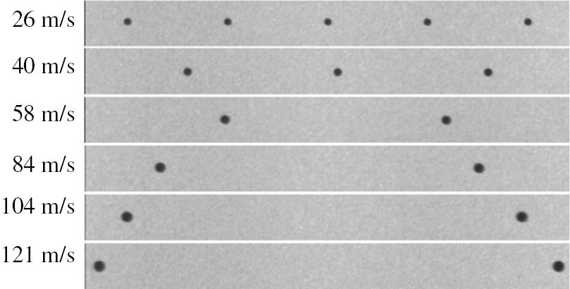
Higher-velocity droplets arrive at the target location with greater spacing.
As the desired performance of the droplet generator has been realized, lifetime and overall reliability of the droplet generators on EUV sources have become the focus of development efforts. Most important breakthroughs have been on the materials science side of the technology. Additionally, recent significant advances in protecting tin from contamination have paved the way for radical transformations of the droplet-generation system architecture with emphasis on preventing tin supply from limiting the operational runtime of the droplet generator.
6 Pre-pulse technology
The typical size of a Sn droplet is significantly smaller than the laser beam diameter at its focal position. For this reason, further ‘conditioning’ of the target needs to take place once the droplets have left the droplet generator. This is achieved by the use of a pre-pulse as shown in Figure 12.
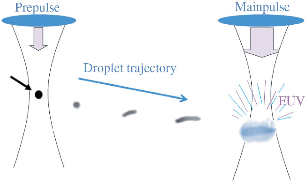
Pre-pulse (pp) concept drawing showing expansion of the Sn droplet to match the main pulse (MP) beam waist diameter and lower the density of the target material.
The size and material distributions of formed targets using pre-pulse are critical for CE and EUV power scaling. In addition to these parameters, target density and its profile, and volume distribution of target material are crucial for further improvement of CE and EUV power scaling. Coupling of the main pulse with an optimized target leads to higher CE, manageable debris, and improved EUV power scaling. Figure 13A shows a shadowgraph of a typical low density target generated with pre-pulse technologies. For comparison, Figure 13B shows a disk target. An optimized tin target has lower density than a liquid target, and when irradiated by the main drive laser pulse, a plasma without a steep density gradient is created.
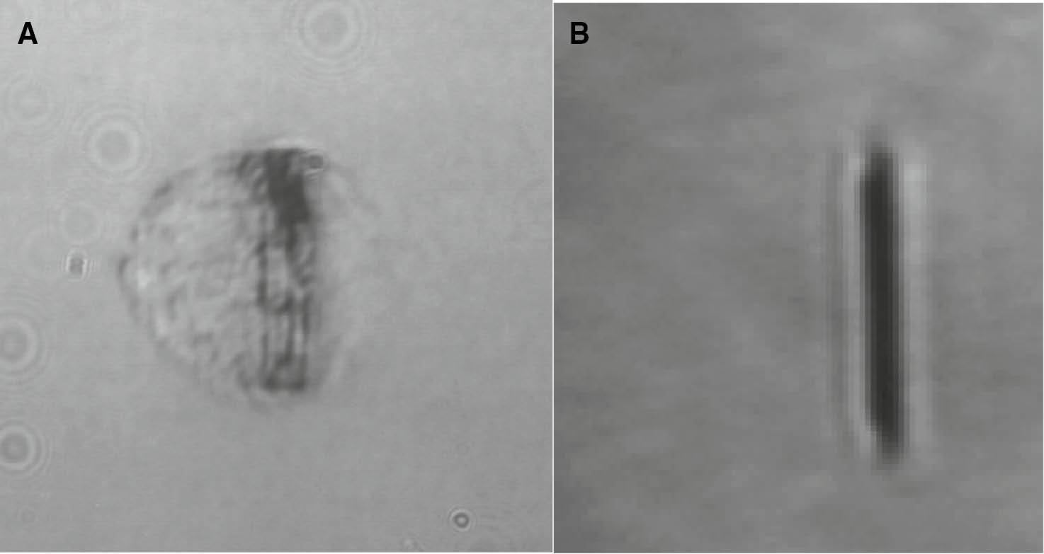
Side view shadowgrams of the targets after irradiation by different pre-pulses, (A) spherical target, (B) disk target.
More efficient use of target material and more efficient laser absorption are obtained by creating distributed laser absorption instead of localized laser absorption. More Sn ions are involved to emit EUV leading to higher conversion efficiency. With lower density targets, higher conversion efficiency and EUV power were demonstrated (shown in Figure 14) [24]. CE of 6% and 375 W in-burst EUV power at low duty cycle has been demonstrated on test sources in development laboratories [24], as shown in Figures 14 and 15.
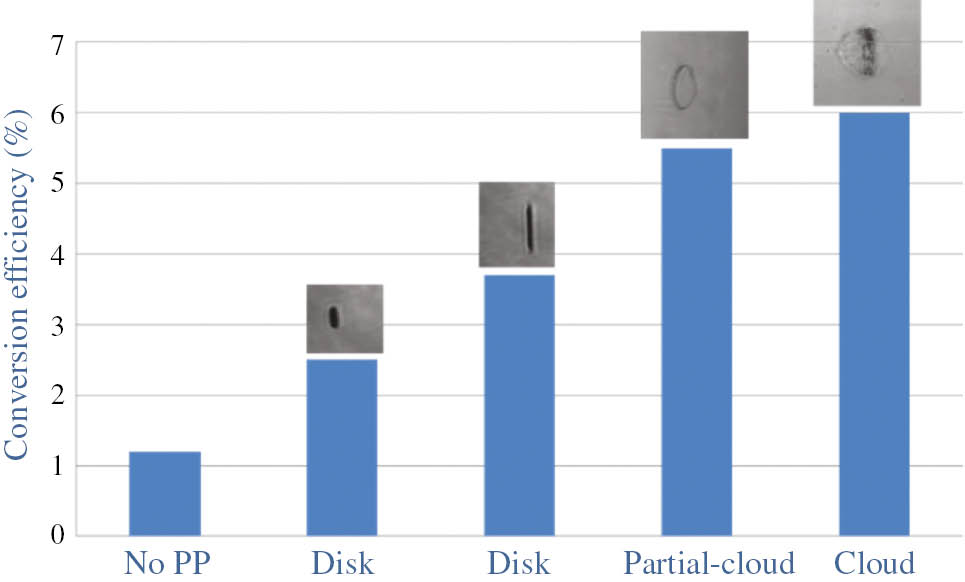
Conversion efficiency with various target shapes and densities.
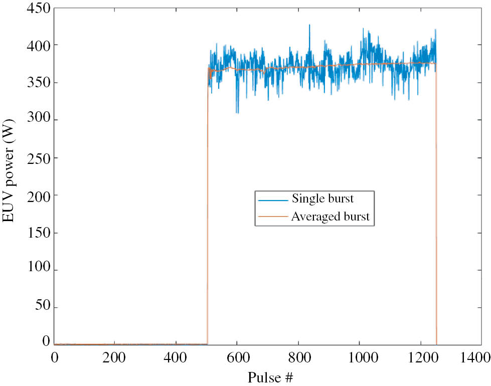
A 350-W in-burst EUV power obtained with low density target.
Uniform low density tin targets without steep gradients not only enhances EUV generation but also reduces the kinetic energy of ions. During the plasma expansion, a static electric field is setup due to separation of fast electrons and slower ions. This electric field accelerates ions from its plasma temperature, i.e. several 10 eV, up to several keV depending on plasma density profile. The electric field can be described as inversely proportional to plasma density gradient, which means a lower plasma density gradient leads to longer plasma length, resulting in lower electric field and lower kinetic energy of ions. This means that a low density target also helps Sn debris mitigation and optics lifetime.
7 EUV collector and debris mitigation
An advantage of LPP sources is the isolated nature of the plasma, with open access to the EUV emission pattern over the full 4π sr; however, typically only ∼2π sr hemisphere can be used to collect EUV. A sample picture of a collector with 5.5 sr collecting angle is shown in Figure 16. The challenge is to achieve high reflectance over the full surface of the collector, accepting the fact that when the angle of incidence approaches 45°, only the s-polarized light is reflected. The infrastructure for manufacturing of large-size normal-incidence collector mirrors is already in place. A large number of collectors have been fabricated for NXE sources.
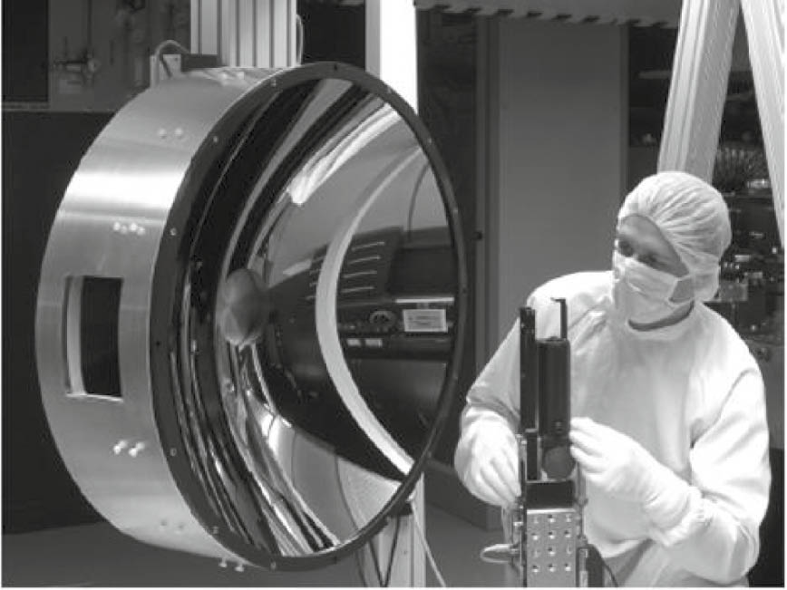
Picture of a normal incidence EUV collector used in the ASML NXE 3100 source.
Achieving long collector lifetime is one of the most difficult challenges for the introduction of EUV lithography into HVM. The source environment within the vacuum vessel needs to be taken into account as high-energy ions and neutrals from the plasma could strike the collector surface and cause irreversible damage. To protect the multilayer reflective coating, hydrogen buffer gas may be used within the vacuum chamber to slow down the high-energy ions, along with special collector capping layers.
Improvements in the efficacy of the debris-mitigation techniques implemented in the LPP source resulted in longer lifetime achieved in actual sources operating in the field, as can be seen in Figure 17, showing (A) the history of collector lifetime improvement and (B) typical collector reflectivity vs. number of pulses for two samples of NXE 3300 collectors (b). Over 100 Billion pulses collector lifetime has been demonstrated [26]. As the source power increased, collector protection needs to be adapted to increase the lifetime of EUV collectors. A tin cleaning technique using hydrogen radicals was developed to enhance the rate of tin removal from the collector. The combination of continued improvements in Sn management inside the EUV source vessel and assisted tin cleaning provides a path toward the lifetime requirement of 30000 h mentioned earlier.
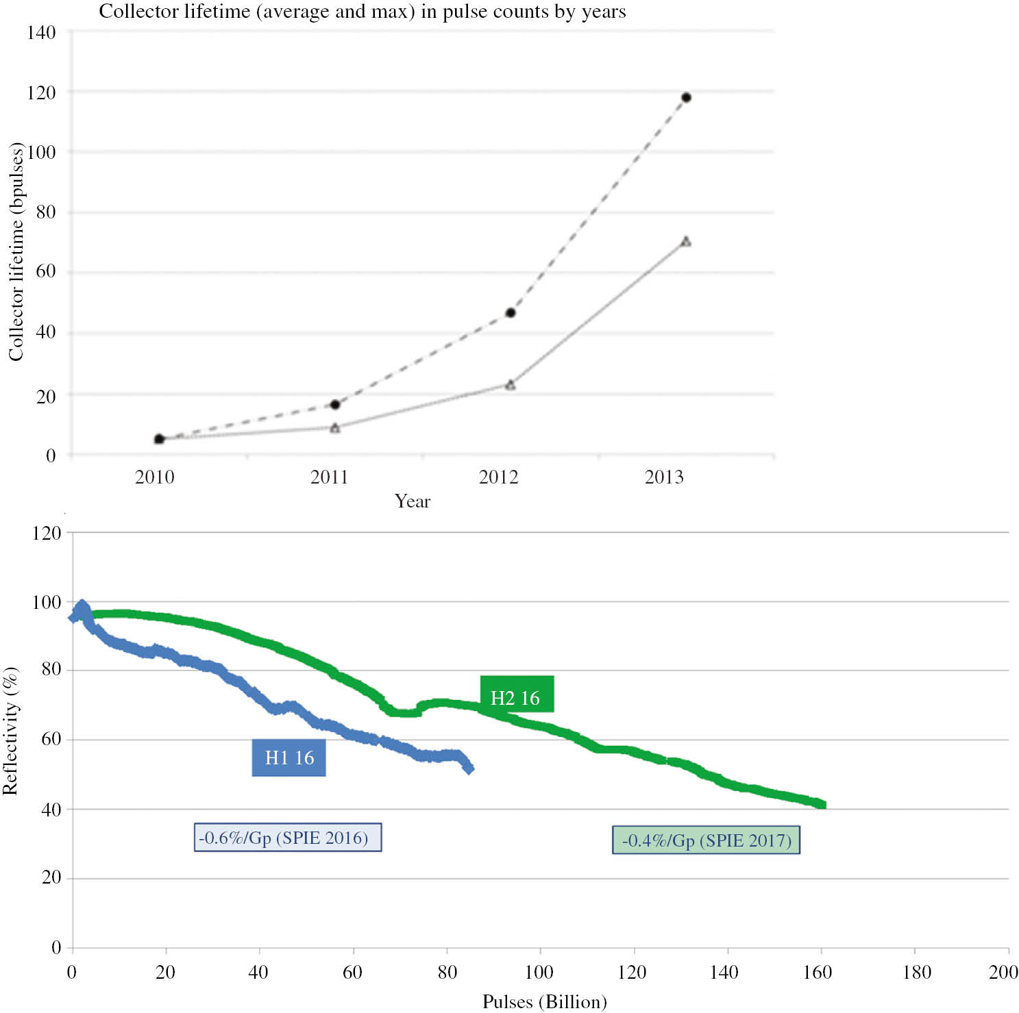
Improvements in NXE-3300 collector lifetime (A) and typical collector reflectivity change throughout the lifetime (B).
Debris mitigation in the source relies on using hydrogen as a buffer gas. There are several requirements for the buffer gas in the EUV source. It has to efficiently cool the region near the plasma, it has to efficiently stop fast Sn ions, and it should be able to efficiently etch Sn from the collector surface. It has to do all these three functions without imposing excessively high EUV absorption. Typically, maximum EUV absorption by the buffer gas of 20–30% is accepted in the EUV power budget. Last, but not the least, the buffer gas has to be economical for the quantities that are required for the source operation. Hydrogen satisfies all these requirements and is the preferred choice for a buffer gas. Figure 18 illustrates, for example, the stopping power of hydrogen gas for Sn ions generated by laser plasma.
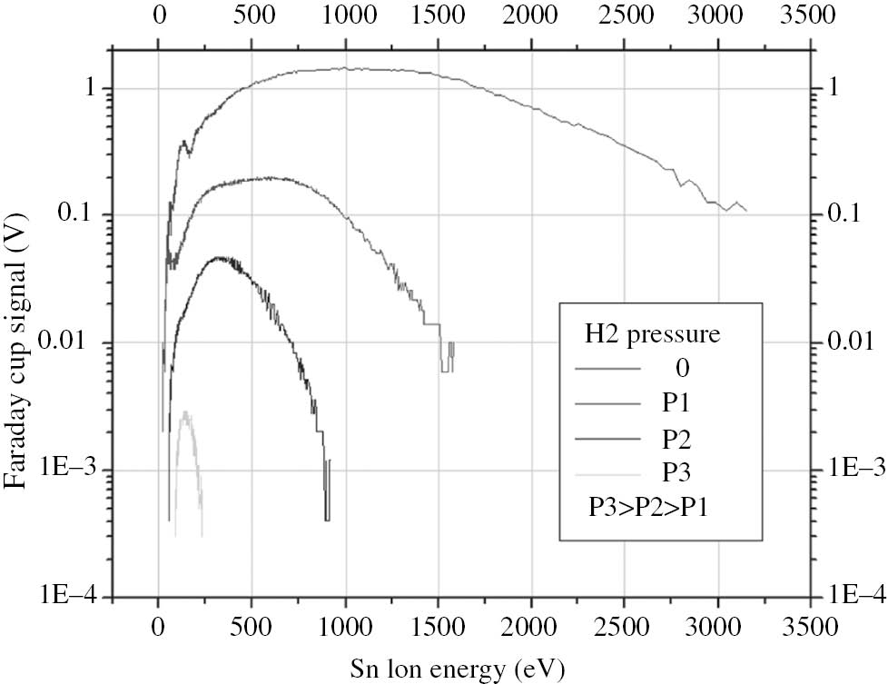
Hydrogen buffer gas pressure vs. ion energy and flux at the location of the collector surface.
In addition to being the best gas for thermal properties and stopping ions, hydrogen also happens to be a good etchant for Sn. This is quite fortunate because it allows to use pure hydrogen in the source without adding any additives to etch Sn. Sn etching with hydrogen is described by the following reaction:
Hydrogen radicals ·H are produced in the source by dissociation of molecular hydrogen:
Dissociation of molecular hydrogen happens by several mechanisms in the source: thermal dissociation in the plasma region, photo-dissociation by plasma radiation, dissociation by photo-electrons.
Once SnH4 (stannane) is formed, it can be pumped away as it is gas under the source conditions. However, competing mechanisms are photo-dissociation of stannane and catalytic dissociation on Sn-covered surfaces. These mechanisms tend to bring Sn back to collector surfaces, thus, reducing the cleaning rate. The goal of debris mitigation is to minimize the residence time of stannane in the vessel and reduce the number of wall collisions of stannane molecules, thus, reducing the effects of Sn redeposition due to stannane dissociation. The total Sn cleaning rate is thus:
where Knet is the net etch rate of Sn, KSnH4_formation is the rate of SnH4 formation, and KSn_redep is the rate of Sn redeposition.
All debris that need to be taken care of in the source can be divided into two large categories, primary and secondary debris. Primary debris is the one that comes directly from the plasma before collision with any surface or before being trapped by the gas flows in the source. In addition to Sn material, the kinetic energy of fast ions is released into the buffer gas. Plasma radiation is partially absorbed by the gas. These two effects do not directly lead to collector reflectivity degradation, but it affects the debris mitigation performance by heating up the gas and decreasing its density in the volume between the plasma and the collector surface. To reduce this effect, fresh gas has to be flown constantly into the vessel at high flow rates.
Secondary debris consists of all debris that collided with surfaces such as the vessel walls. This includes Sn microparticles that scattered back to the collector or are otherwise transported back to the collector surface. Secondary debris also includes Sn material accumulating inside the vessel. Sn accumulation can lead to Sn debris protruding into the EUV or CO2 optical path, impeding the vacuum exhaust path and, thus, changing the gas flow in the vessel as well as accumulated Sn falling or dripping onto the collector surface as it is facing up against gravity in the EUV source.
Another application that hydrogen is used for is protection of the scanner volume (illumination optics) from debris generated in the source as the scanner has many optical surfaces that are very expensive to replace and are very sensitive to contamination. Primary microparticles generated at plasma location are usually blocked by a small obscuration in direct line of sight from the plasma to the intermediate focus. This way, virtually 100% of all primary debris can be blocked from traveling into the scanner volume. There is, however, still a risk of secondary debris penetrating into the scanner. This risk is minimized by careful design of internal hardware of the source vessel. As we can see, hydrogen as a buffer gas provides several functions for Sn management, the most important being reduction of Sn flux to the collector, etching Sn from the collector, cooling the plasma region, and carrying debris out of the vessel.
8 Summary and future outlook
Laser-produced plasma sources have been shown to be the leading technology with scalability to meet the requirements of ASML scanners and provide a path toward higher power needed by lithography tools as they evolve over their life cycle. More than 10 LPP sources have been used by leading edge chipmaker R&D sites around the world, accumulating the necessary knowledge and know-how to eventually move into the HVM environment. MOPA pre-pulse technology has been validated as the path to higher power output, and stabilized power of 210 W at intermediate focus has been demonstrated, using advanced control technology to meet the dose stability target of <±0.5% 3σ with reduced dose margin. Normal-incidence collector mirrors with >5 sr light collection and high average reflectivity are being produced in volume and are showing increasingly long lifetimes in the field. Enhanced collector protection and in situ cleaning technologies on the NXE 3350B source are both expected to increase lifetime further. NXE 3400B sources are being installed at the customer’s facilities in 2017.
About the authors
Igor Fomenkov is an ASML Fellow in Technology Development Group in San Diego, California. After completing a PhD in Physics and Mathematics at Moscow Institute of Physics and Technology (MPTI) in 1986, he joined General Physics Institute as a senior scientist, where he worked in the field of interaction of high intensity laser radiation with matter and diagnostics of laser produced plasma. He joined Cymer in 1992 and worked on the development of high power, high reliability KrF and ArF Excimer lasers for DUV (at 248 nm and 193 nm) microlithography. Since 1997 he has been conducting research and development of sources for Extreme Ultraviolet Lithography at 13.5 nm. Over several years of research on EUV light generation, based on Discharge Produced Plasma and Laser Produced Plasma, he has been involved in defining the source architecture, namely Laser Produced Plasma EUV source using high power, high repetition rate CO2 laser and tin droplets as source target material and development of the source for High Volume Manufacturing. He was appointed Cymer Fellow in 2003 and ASML Fellow in 2014. He has authored over 50 technical papers in the field of Laser Produced Plasma, DUV lasers and sources for EUV lithography, and holds over 100 patents in the areas of DUV and EUV light sources.
Alexander Schafgans is a principal scientist at Cymer/ASML, the global leader in developing light sources used by the semiconductor industry to pattern advanced logic and memory. In his role at Cymer, Schafgans has been focused on leading EUV power scaling activities from 10 W through 500 W. During his PhD in Physics, Schafgans focused on the infrared and optical properties of correlated electron materials and graduated from UC San Diego in 2011.
Slava Rokitski is a Senior Manager of System Design at Cymer, an ASML company. He received a PhD degree in electrical engineering at the University of California, San Diego, where he performed research on real-time ultrafast optical information processing and detection. At Cymer Slava has been developing technologies for 193 nm and 248 nm high power excimer laser systems for DUV lithography. Most recently Slava has been developing technologies for high power CO2 master-oscillator-power-amplifier laser systems, used in laser produced plasma extreme ultraviolet light sources.
Michael Purvis serves as the Systems Power Architect for the EUV Source Program at ASML San Diego. Over the last decade, Michael has published in the field of laser created plasmas. His initial investigations at Colorado State University included developing discharge and laser produced EUV lasers for applications in plasma diagnostics, after which he worked on theoretical plasma modelling and high energy density experiments at CSU, Lawrence Livermore National Labs and SLAC. He is now applying his experience with plasmas generated in the femtosecond to nanosecond time scales towards the development of EUV light sources at ASML.
Silvia De Dea received her PhD in Chemical Engineering from The University of California, San Diego in 2008. Her research interests include novel nanomaterials and analytical instruments, materials development for extreme conditions and EUV light technology. She has been with Cymer (now ASML) since 2008 focusing on technology development of EUV sources for semiconductor lithography. She is a Principal Scientist with ASML working on EUV optics lifetime and materials performance.
Jayson Stewart received his PhD in Physics from the University of Colorado in 2009. His research interests focus on light-matter interactions and EUV light source development. In 2012, Jayson joined the ASML team as a research scientist to work on the EUV light source within the technology development group. His work focuses on managing the debris resulting from the laser produced plasma.
Matthew Graham received his PhD in Mechanical Engineering from University of California San Diego in 2007. In 2008 he joined Cymer/ASML working on the DUV light source control system and in 2009 transitioned to development of the EUV light sources for semiconductor lithography. He is currently a Staff Engineer working on control systems around the plasma generation process in the EUV light source.
Daniel J. Riggs has a BS in Mechanical Engineering, a BA in Mathematics: Applied Science, and an MS and PhD in Engineering Science, all from the University of California, San Diego (UCSD). He has worked as a control systems engineer at Cymer since 2006. For the first several years, his focus was high performance control system development for Cymer’s DUV laser products. Since 2009, his focus has been EUV system and control system architecture and design.

Daniel Brown currently serves as Vice President of Technology Development for ASML San Diego. In this role since 2010, he previously held the positions of Vice President, Technology Development and Vice President, Engineering within the Deep-Ultraviolet Product Group in Cymer, Inc. In his current role, he is chartered with overseeing the technology activities for the company’s EUV light source development and deep-ultraviolet light source products to meet the demands of the semiconductor marketplace. Prior to joining Cymer in 2000, Brown a served for over 11 years in various Australian Research Council Fellow positions at Macquarie University (located in Sydney, Australia) including Australian Senior Research Fellow and Australian Research Fellow, responsible for development of novel high-power ultraviolet laser sources based on nonlinear frequency conversion of high-pulse-rate laser systems. Dr. Brown holds a Doctorate degree in physics and a Bachelor’s degree in science from the University of New England in Australia.
References
[1] G. D. Kubiak and D. R. Kania, Eds., in ‘OSA Proceedings on Extreme Ultraviolet Lithography’, (Optical Society of America, Washington DC, 1995) Vol. 23.Search in Google Scholar
[2] G. Kubiak, L. Bernardes, K. D. Krenz, D. O’Connell, R. Gutowski, et al., in ‘OSA Trends in Optics and Photonics, Vol. 4, Extreme Ultraviolet Lithography’, Eds. By G. D. Kubiak and D. R. Kania (Optical Society of America, Washington, DC, 1996) pp. 66–71.10.1364/EUL.1996.ES66Search in Google Scholar
[3] EUV Sources for Lithography, Ed. By V. Bakshi, Volume PM149 (SPIE, 2006).Search in Google Scholar
[4] T. Tomie, J. Micro./Nanolith. MEMS MOEMS 11, 021109 (2012)10.1117/1.JMM.11.2.021109Search in Google Scholar
[5] A. Endo, J. Mod. Phys. 5, 285–295 (2014).10.4236/jmp.2014.55039Search in Google Scholar
[6] R. Peeters, S. Lok, E. van Alphen, N. Harned, P. Kuerz, et al., in ‘Proc. SPIE Extreme Ultraviolet (EUV) Lithography III’, Ed. By P. P. Naulleau, 8679, 86791F (2013).10.1117/12.2010932Search in Google Scholar
[7] D. C. Brandt, I. V. Fomenkov, A. I. Ershov, W. N. Partlo, D. W. Myers, et al., in ‘Proc. of SPIE, Alternative Lithographic Technologies’, Eds. By F. M. Schellenberg and B. M. La Fontaine, Vol. 7271, 727103, (2009).10.1117/12.814228Search in Google Scholar
[8] I. V. Fomenkov, D. C. Brandt, A. N. Bykanov, A. I. Ershov, W. N. Partlo, et al., in ‘Proc. of SPIE, Alternative Lithographic Technologies’, Eds. By F. M. Schellenberg and B. M. La Fontaine, Vol. 7271, 727138 (2009).10.1117/12.814272Search in Google Scholar
[9] N. R. Böwering, I. V. Fomenkov, D. C. Brandt, A. N. Bykanov, Ershov, et al., J. Micro/Nanolith. MEMS MOEMS 8, 041504 (2009).10.1117/1.3224942Search in Google Scholar
[10] D. C. Brandt, I. V. Fomenkov, A. I. Ershov, W. N. Partlo, D. W. Myers, et al., in ‘Proc. of SPIE, Extreme Ultraviolet (EUV) Lithography II’, Eds. By B. M. La Fontaine and P. P. Naulleau, Vol. 7969, 79691H (2011).10.1117/12.882208Search in Google Scholar
[11] H. Mizoguchi, H. Nakarai, T. Abe, K. M. Nowak, Y. Kawasuji, et al., in ‘Proc. of SPIE, Extreme Ultraviolet (EUV) Lithography VI’, Eds. By Obert R. Wood II and Eric M. Panning, Vol. 9422 (2015).10.1117/12.2086347Search in Google Scholar
[12] D. C. Brandt, I. V. Fomenkov, M. J. Lercel, B. M. La Fontaine, D. W. Myers, et al., in ‘Proc. SPIE, Extreme Ultraviolet (EUV) Lithography III’, Eds. By P. P. Naulleau and Obert R. Wood II, Vol. 8322, 83221I (2012).10.1117/12.916521Search in Google Scholar
[13] I. V. Fomenkov, N. R. Böwering, D. C. Brandt, D. J. Brown, A. N. Bykanov, et al., in ‘Proc. SPIE Extreme Ultraviolet (EUV) Lithography III’, Eds. By P. P. Naulleau and Obert R. Wood II, Vol. 8322, 83222N (2012).10.1117/12.916531Search in Google Scholar
[14] D. C. Brandt, I. V. Fomenkov, A. I. Ershov, W. N. Partlo, D. W. Myers, et al., in ‘Proc. Of SPIE, Emerging Lithographic Technologies XI’, Ed. By M. J. Lercel, Vol. 6517, 65170Q (2007).10.1117/12.713279Search in Google Scholar
[15] I. V. Fomenkov, B. A. M. Hansson, N. R. Böwering, A. I. Ershov, W. N. Partlo, et al., in ‘Proc. of SPIE, Emerging Lithographic Technologies X’, Ed. By M. J. Lercel, Vol. 6151, 61513X (2006).10.1117/12.655733Search in Google Scholar
[16] I. V. Fomenkov, D. C. Brandt, A. N. Bykanov, A. I. Ershov, W. N. Partlo, et al., in ‘Proc. of SPIE, Emerging Lithographic Technologies XI’, Ed. By M. J. Lercel, Vol. 6517, 65173J (2007).10.1117/12.713454Search in Google Scholar
[17] I. V. Fomenkov, A. I. Ershov, W. N. Partlo, D. W. Myers, D. Brown, et al., in ‘Proc. of SPIE, Extreme Ultraviolet (EUV) Lithography II’, Eds. By B. M. La Fontaine and P. P. Naulleau, Vol. 7969, 796933 (2011).10.1117/12.882210Search in Google Scholar
[18] A. Pirati, R. Peeters, D. Smith, S. Lok, M. van Noordenburg, et al., in ‘Proc. of SPIE, Extreme Ultraviolet (EUV) Lithography VII, Eds. By E. M. Panning and K .A. Goldberg, Vol. 9776, 97760A-1 (2016).10.1117/12.2220423Search in Google Scholar
[19] M. Van den Brink, in ‘Proceedings of EUVL Symposium’, October 2015, Maastricht, NL, euvlsymposium.lbl.gov/pdf/2015.Search in Google Scholar
[20] R. Burdt, T. Duffey, J. Thornes, T. Bibby, R. Rokitsky R., et al., in ‘Proc. SPIE, Optical Microlithography XXVII’, Eds. By L. Kafai and A. Erdmann, Vol. 9052, 90522K-1 (2014).10.1117/12.2048082Search in Google Scholar
[21] I. V. Fomenkov, D. C. Brandt, N. R. Farrar, B. La Fontaine, D. W. Myers, et al., in ‘Proc. of SPIE, Extreme Ultraviolet (EUV) Lithography V’, Eds. By O. A. Wood II and E. M. Panning, Vol. 9048, 904835-1 (2014).Search in Google Scholar
[22] I. Fomenkov, B. La Fontaine, D. Brown, I. Ahmad, P. Baumgart, et al., J. Micro/Nanolith. MEMS MOEMS 11, 021110 (2012).10.1117/1.JMM.11.2.021110Search in Google Scholar
[23] A. A. Schafgans, D. Brown, I. Fomenkov, R. Sandstrom, A. Ershov, et al., in ‘Proc. of SPIE, Extreme Ultraviolet (EUV) Lithography VI’, Eds. By O. R. Wood II and E. M. Panning, Vol. 9422, 94220B-1 (2015).10.1117/12.2087421Search in Google Scholar
[24] I. Fomenkov, in ‘Proceedings of 2015 International Workshop on EUV Lithography’, June 15–19, 2015, Maui, Hawaii, P3. www.euvlitho.com.Search in Google Scholar
[25] I. V. Fomenkov, A. I. Ershov, W. N. Partlo, D. W. Myers, R. L. Sandstrom, et al., in ‘Proc. of SPIE, Extreme Ultraviolet (EUV) Lithography’, Ed. By B. M. La Fontaine, Vol. 7636, 763639-1 (2010).10.1117/12.848408Search in Google Scholar
[26] D. C. Brandt, I. V. Fomenkov, N. R. Farrar, B. La Fontaine, D. W. Myers, et al., in ‘Proc. of SPIE, Extreme Ultraviolet (EUV) Lithography V’, Eds. By O. R. Wood II and E. M. Panning, Vol. 9048, 90480C-1 (2014).10.1117/12.2048184Search in Google Scholar
©2017 THOSS Media & De Gruyter, Berlin/Boston
Articles in the same Issue
- Cover and Frontmatter
- Views
- Patterning roadmap: 2017 prospects
- Community
- Conference Notes
- News from the European Optical Society (EOS)
- Topical issue: Optical Nanostructuring
- Editorial
- Next-generation lithography – an outlook on EUV projection and nanoimprint
- Tutorial
- Photoresists in extreme ultraviolet lithography (EUVL)
- Review Articles
- Light sources for high-volume manufacturing EUV lithography: technology, performance, and power scaling
- Characterization and mitigation of 3D mask effects in extreme ultraviolet lithography
- EUV mask defectivity – a process of increasing control toward HVM
- Development and performance of EUV pellicles
- A review of nanoimprint lithography for high-volume semiconductor device manufacturing
- Large area nanoimprint by substrate conformal imprint lithography (SCIL)
- Laser interference patterning methods: Possibilities for high-throughput fabrication of periodic surface patterns
- Research Articles
- A full-process chain assessment for nanoimprint technology on 200-mm industrial platform
- Challenges of anamorphic high-NA lithography and mask making
- Research Article
- Chip bonding of low-melting eutectic alloys by transmitted laser radiation