Silicon photonics WDM transmitter with single section semiconductor mode-locked laser
-
Juliana Müller
Juliana Müller is currently a doctoral student at the Institute for Integrated Photonics of RWTH Aachen University. Her current research focuses on resonant ring modulators for WDM transceivers. From 2007 to 2013, she studied Electrical Engineering at RWTH Aachen University with a focus on micro- and nano-electronics. She received her Master’s degree in 2013.
 ,
Johannes Hauck
,
Johannes Hauck
Johannes Hauck is a doctoral student at the Institute for Integrated Photonics of RWTH Aachen University. The focus of his current research lies with silicon photonic systems with a particular emphasis on coherent wavelength division multiplexed transceivers. From 2005 to 2011, he studied Physics at RWTH Aachen University with focus on optical systems, laser technology, extreme-ultraviolet optics and solid-state physics. He received his Dipl.-Phys. degree from RWTH Aachen University in 2011.
Bin Shen received his BSc in Material Science and Engineering from the Zhejiang University of Technology (China) with a focus on Polymer Science in 2008 and his MSc in Material Science with a focus on Nanotechnology and Electric Materials from RWTH Aachen University in 2012. He joined the Institute for Integrated Photonics of the RWTH Aachen in 2011 as a Master Student and is now working toward a PhD degree in Electrical Engineering. After working on test automation methodologies, the focus of his current research is on nonlinear optical devices.
Sebastian Romero-García received the Ingeniero de Telecomunicación degree from the University of Malaga, Spain, in 2009. From 2009 to 2011, he was a Research Assistant at the Department of Communications Engineering, University of Malaga. Since 2011, he has been with the Institute for Integrated Photonics of RWTH Aachen University where he is currently working toward the PhD degree in Electrical Engineering. His research interests focus on the development of integrated photonic devices and systems. Recent publications cover the development of a SiN back-end waveguide technology for biosensing, as well as the development of alignment tolerant couplers for hybrid Silicon Photonics system integration.
Elmira Islamova received a Bachelor’s degree in Telecommunications from SPbNRU ITMO (St. Petersburg, Russia) in 2013 and is now studying toward a Master’s degree in Communications Engineering at RWTH Aachen University. She is currently doing research at the Institute for Integrated Photonics with a primary focus on the characterization of integrated silicon ring-resonator modulators and add-drop multiplexers.
Saeed Sharif Azadeh joined the Institute for Integrated Photonics of RWTH Aachen University as a PhD student in July 2012. His PhD project includes the simulation and design of silicon photonics electro-optical modulators, device fabrication, and high frequency device characterization. He received his MSc in Electrical Engineering from Sharif University of Technology (Iran) in 2011 where he investigated optical properties of HTC superconductor devices.
Siddharth Joshi received his Integrated MSc degree in Photonics from Cochin University of Science and Technology (India) in 2011 and a PhD degree in Optical Telecommunications from Université Pierre et Marie Curie (France). During his PhD as a Marie Curie early stage researcher, he worked at III–V Lab on conception and fabrication of low-chirp and low-phase noise optical sources based on quantum dash nano-structures. Presently, he is working at Institut Electronique Fondametale (France) toward the development of terahertz quantum cascade lasers.
Nicolas Chimot received the Master’s diploma in Light and Matter Interaction in 2003 from the University of Rennes I and the PhD degree in 2006 from the University of Paris XI. His PhD work was focused on the development of photoconductive emitters and detectors driven at 1550 nm for the generation of terahertz electromagnetic waves and the conception of ultrafast photo switches. From 2006 to 2008, he was a postdoctoral Researcher at Molecular Electronic Laboratory at Commissariat à l’Energie Atomique at Saclay, France. He worked on the conception of carbon nanotube-based transistors on flexible substrate for high-frequency applications and on the conception of nanoelectromechanical devices with carbon nanotubes. Since 2008, he has works at the III–V Lab, Alcatel-Lucent, in the Photonic Integrated Circuit team. He is currently involved in the optimization and characterization of QD-based lasers for telecommunication applications.
Alvaro Moscoso-Mártir received his MSc degree in Telecommunications Engineering from Málaga University (Spain) in 2008 and his PhD degree in Microwave Engineering from Málaga University in 2013. During his PhD, he focused on the design of ultra-wideband radiofrequency circuitry in integrated planar technology for six-port receivers. Currently, he is working as a Postdoctoral Scholar at the Institute for Integrated Photonics of the RWTH Aachen, where his main research activities focus on the design of microwave circuits and components and on the modeling and assembly of optoelectronic components.
Florian Merget received his Dipl.-Ing. and his PhD in Electrical Engineering from RWTH Aachen University (Germany) in 2002 and 2008. During his PhD, he worked on electrical and optical chalcogenide phase change memory devices and specialized on semiconductor fabrication technologies. In 2008, he joined the Silicon Photonics Group of the Institute of Semiconductor Electronics (led by Prof. H. Kurz) as a project manager. In 2011, he joined the newly established Silicon Photonics Laboratory as a staff scientist. His main research interests focus on complex and high-speed data transmission systems and electro-optic components that are specifically targeted to meet the needs of next-generation telecom and datacom applications.
François Lelarge received the Diploma in Material Science in 1993 and the PhD degree in 1996, both from the University of Pierre et Marie Curie, Paris, France. From 1993 to 1996, he was with the Laboratory of Microstructures and Microelectronic, CNRS Bagneux, France. His thesis work was devoted to the fabrication and the optical characterization of GaAs/AlAs lateral superlattice grown on vicinal surfaces by MBE. From 1997 to 2000, he was a postdoctoral researcher at the Institute of Micro and Optoelectronics, Lausanne, Switzerland. He worked on InGaAs/GaAs quantum wires fabrication by MOCVD regrowth on patterned substrates. Presently, he is in charge of the Epitaxy and New Material Technology team within III–V Lab and coordinator of a project on QD-based directly modulated lasers (ANR-DIQDOT). He has published more than 110 papers and communications in national and international conferences, including invited talks and postdeadline papers on QDot-based devices.
Jeremy Witzens has been leading the Institute for Integrated Photonics of the RWTH Aachen since 2011. Prior to joining the RWTH, he was a Principal Research Scientist at the University of Washington (2009–2010), a Sr. Staff Engineer at Luxtera Inc. (2006–2009), a Postdoctoral Scholar at the California Institute of Technology (2005), and an Integrated Optics Designer at Luxtera Inc. (2002–2003). He received his PhD from the California Institute of Technology in 2005, where he worked on Photonic Crystal Micro-Cavities and Photonic Crystal-based light steering devices, and his Engineering Diploma from the Ecole Polytechnique (Palaiseau, France). He has been working on Silicon Photonics since 2002, co-authored papers and co-invented patents on topics such as germanium waveguide photodetectors, silicon electro-optic modulators, WDM and add-drop multiplexers, optical fiber- and laser-to-chip couplers, and photonic-electronic integration. His current research interests include high-performance Silicon Photonics modulators, alignment-tolerant optical chip couplers, comb light sources, group IV light sources, advanced transceiver architectures, hybrid photonic integration, and biophotonics. He received an ERC award in 2011 and is currently coordinating the European project ‘Broadband Integrated and Green Photonics Interconnects for High-Performance Computing and Enterprise Solutions’ (BIG PIPES).

Abstract
We demonstrate a wavelength domain-multiplexed (WDM) optical link relying on a single section semiconductor mode-locked laser (SS-MLL) with quantum dash (Q-Dash) gain material to generate 25 optical carriers spaced by 60.8 GHz, as well as silicon photonics (SiP) resonant ring modulators (RRMs) to modulate individual optical channels. The link requires optical reamplification provided by an erbium-doped fiber amplifier (EDFA) in the system experiments reported here. Open eye diagrams with signal quality factors (Q-factors) above 7 are measured with a commercial receiver (Rx). For higher compactness and cost effectiveness, reamplification of the modulated channels with a semiconductor optical amplifier (SOA) operated in the linear regime is highly desirable. System and device characterization indicate compatibility with the latter. While we expect channel counts to be primarily limited by the saturation output power level of the SOA, we estimate a single SOA to support more than eight channels. Prior to describing the system experiments, component design and detailed characterization results are reported including design and characterization of RRMs, ring-based resonant optical add-drop multiplexers (RR-OADMs) and thermal tuners, S-parameters resulting from the interoperation of RRMs and RR-OADMs, and characterization of Q-Dash SS-MLLs reamplified with a commercial SOA. Particular emphasis is placed on peaking effects in the transfer functions of RRMs and RR-OADMs resulting from transient effects in the optical domain, as well as on the characterization of SS-MLLs in regard to relative intensity noise (RIN), stability of the modes of operation, and excess noise after reamplification.
1 Introduction
Short distance (up to 2 km) wavelength domain multiplexed (WDM) electro-optic (E/O) transceiver solutions relying on single-mode fiber (SMF) have moved into the spotlight for data center applications with the release of three independent 100G multi-source agreements (MSAs) in 2014 based on 4×25 Gbps on-off keying (OOK) signaling, CWDM4 [1], CLR4 [2], and Open Optics [3]. With growing data center dimensions, a need for longer reach data center interconnects has been identified [4, 5], making a transition toward SMF-based solutions attractive despite more stringent alignment tolerances during assembly. With increasing channel count, e.g., with the C-Form-Factor Pluggable (CFP) roadmap including form factors with up to 16 channels and increasing link distances, solutions relying on WDM rather than on parallel optics (with multiple fibers) are also becoming more effective despite the additional complexity associated with the implementation of a WDM system.
Comb sources, i.e., light sources that generate multiple mode-locked optical carriers on a fixed grid (the comb lines), are very attractive in this context since they can be very compact and could reduce cost due to the small number of required devices (depending on the implementation down to a single semiconductor laser). Furthermore, the channel spacing is often a static comb source characteristic that does not need to be controlled, so that it suffices to actively control the wavelength of a single comb line to snap the entire comb to a WDM grid [6]. Various compact comb sources have been demonstrated, including single section semiconductor mode-locked lasers (SS-MLLs) [7–10], semiconductor mode-locked lasers with saturable absorber [11, 12], integrated optical parametric oscillators (OPOs) relying on the Kerr effect in integrated microcavities [13–16], and gain switched comb sources [17]. Here, we will focus on SS-MLLs in which the individual comb lines are mode locked within a Fabry-Perot semiconductor laser cavity by means of nonlinear optical effects. While the mode locking, itself, is not directly leveraged for the OOK systems investigated here, it is indirectly an essential property of the lasers, as it allows reducing the relative intensity noise (RIN) of individual comb lines by suppressing the mode partition noise while maintaining a flattop laser spectrum with a homogeneous distribution of the optical power among the comb lines [6, 18]. SS-MLLs generate the optical comb without requiring additional devices, making them both the most cost effective and the most compact light source for integrated WDM systems. While their performance in terms of RIN and of optical linewidth does not yet reach that of the other aforementioned solutions, they have the highest wall plug efficiency as the other solutions incur additional optical losses or electrical power consumption associated with auxiliary devices (optical cavity, auxiliary injection locked laser). As shown in the following, the performance of current C-band SS-MLLs is sufficient to support multiple 14 Gbps links with integrated SiP modulators and an optical amplifier, with the achievable channel count primarily determined by the optical amplifier characteristics.
Rather than routing the individual comb lines to several modulators via WDM multiplexers [19–21], they can be individually modulated with frequency-selective devices such as high-performance RRMs [22] that can be simply cascaded along a single bus waveguide [23, 24]. While RRMs suffer from a requirement to be tightly thermally stabilized leading to excess power consumption [25], any type of WDM system requires some form of temperature control: at the minimum, the laser(s) need to be temperature controlled to spectrally match the WDM multiplexers [26]. Local thermal tuning of the RRMs can be combined with global temperature stabilization via a Peltier element. While the latter also results in excess power consumption, splitting it over increased aggregate data rates might make the associated power overhead economical in the future. Also relying on ring resonators, RR-OADMs [27] can be used to split the channels in the Rx and route them to individual photodiodes [28, 29]. The E/O S-parameter of a RRM cascaded with a RR-OADM is derived in Section 4 in order to assess their interoperability.
In the next sections, we first individually describe components we have developed (RRMs, RR-OADMs, thermal tuners, SS-MLLs) or characterized together with the SS-MLLs (off-the-shelf commercial SOA) in view of realizing the optical link. We then proceed with a description of the system level experiments. In particular, obtaining sufficiently low RIN on isolated comb lines and maintaining it throughout optical amplification with a SOA has been an important focus of this work. While the final link experiments are done with an EDFA, the data indicates a similar architecture can be demonstrated with a more cost-effective and compact SOA pending the availability of some additional laboratory equipment or revised SiP system chips incorporating customized optical filters. The system experiments shown here enable the evaluation of the link budget for a completely integrated SiP transmitter/receiver solution.
2 Resonant ring modulators
In this section, we review the work we have done to optimize RRMs in view of their utilization in a comb source based transmitter (Tx) system. The embedded high-speed phase shifters rely on the free carrier induced plasma dispersion effect [30] in horizontal reverse biased p(i)n junctions defined by dopant implantation [31] – the most common type of high-speed RRMs due to their relative ease of fabrication. When designing the RRMs, several codependent parameters have to be jointly optimized in order to reach a desired data rate with maximized modulation efficiency. There is a well-known tradeoff between data rate and modulation efficiency [32]: higher resonator Q-factors increase the modulation efficiency and also the photon lifetime and, thus, reduce the optically limited E/O bandwidth. Higher dopant concentrations increase the diode capacitance and, thus, the phase shift efficiency, but also spoil the Q-factor. Carefully adjusting parameters such as waveguide geometry, coupling strength between the ring and the bus waveguide [33], dopant concentrations [34] and the width of the pin diode’s intrinsic region allowed us to optimize the RRMs for several targeted data rates. In order to accurately model the RRMs, transient effects in the optical domain [23, 27, 33, 35–37] have to be taken into account, as we also showed in [38] and [39]. Apart from adjusting design parameters, we are also optimizing the operation of the RRMs by adjusting the detuning between optical carrier frequency and the resonance frequency of the RRM (the optical carrier detuning), taking optical peaking effects into account to optimize the tradeoff between E/O bandwidth and optical modulation amplitude (OMA).
The bandwidth of a RRM is limited by two effects: in the electric domain, the RC time constant of the phase shifter results from the phase shifter’s diode capacitance and series resistance, as well as from the output resistance of a lumped element driver or the characteristic impedance of a connected transmission line. In the optical domain, the photon storage time inside the cavity also limits the E/O bandwidth. The optically limited device bandwidth is often assumed to be

Where fph is the -3 dBe E/O bandwidth limitation of the RRMs as predicted from the optical domain modeling, Q is the loaded Q-factor of the cavity, and fr is the resonance frequency of the ring resonator [40]. An analysis of the transient response of the light to an effective index change in the cavity has, however, shown that this equation, while providing a reasonable first order approximation for a typical RRM operated in OOK modus, is actually inaccurate and requires further refinements for best device optimization. Here, we will summarize these time dynamics in the small signal limit with the formalism used in [38] for RRMs and [39] for RR-OADMs.
We start with the following equations, introduced in [27], describing the time dynamics of the optical field in ring resonators assuming the round trip time to be small compared to other time constants such as the photon lifetime, the inverse radio frequency (RF) modulation frequency or the inverse optical carrier detuning

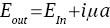
where a is the field amplitude inside the resonator, t is the time, ωr is the angular resonance frequency of the resonator, τa=2Q/ωr is the 1/e decay time of the field amplitude (including both waveguide and coupling losses), μ is the coupling strength between the resonator and the bus waveguide, EIn is the amplitude of the bus waveguide mode incoming toward the RRM, and EOut is the amplitude of the bus waveguide mode outgoing from the RRM. The time-domain coupling parameter μ verifies μ2=κ2vg/L, where κ is the steady-state amplitude coupling parameter between waveguides at the junction to the resonator [41], vg is the group velocity of the waveguide constituting the ring and L its circumference. a has the unit of the square root of an energy (the energy stored inside the resonator), and EIn has the unit of the square root of a power (the incident power), hence, the unit of μ is s-0.5. By applying a sinusoidal drive voltage δV·sin(ωmt), the resonance frequency is shifted to ωr+δωr·sin(ωmt), where the nonlinearity of the transfer function is ignored as we are deriving the small signal S-parameter. We do assume, however, that δωr is a complex number [38] with the imaginary part taking into account the modulation of the free carrier-induced losses that necessarily accompany the refractive index modulation [30]. As a result, the loss modulation enhances the modulation efficiency for optical carrier wavelengths smaller than the resonance wavelength, while it reduces the modulation efficiency for larger optical carrier wavelengths [38]. From Eqs. 2 and 3, one can then derive the time-varying amplitude of the light inside the resonator to be [38]

where ω0 is the angular frequency of the optical carrier, and

where
We used the multi-physics, finite elements method (FEM) modeling software COMSOL (Comsol, Inc., Burlington, USA) as well as Synopsys TCAD (Synopsis Corporate, Mountain View, USA) to determine the change of effective index and optical loss resulting from applying a varying reverse bias voltage to the phase shifter. With the precise modeling of the time dynamics in the optical domain, as given by Eq. 5, and the inclusion of an additional low-pass filter taking into account the RC time constant, this allowed us to predict experimental results very accurately (compare, for example, experimental results and models in Figure 1).

(A) Normalized OMA as a function of coupling point for both families of RRMs and comparison between experimental and simulation data. The coupling point is defined as κ/κ0, where κ0 is the bus waveguide to RRM coupling strength resulting in critical coupling. (B) Normalized OMA as a function of E/O bandwidth and comparison between experimental and simulation data. The coupling point is implicitly varied in this graph.
In [39], we reported a systematic experimental study of the effect of the ring to waveguide coupling strength on the normalized OMA (given by normalized OMA=(P1-P0)/Pin, where Pin is the on-chip power entering the RRM and P1 and P0 are, respectively, the ‘1’ and ‘0’ signal levels after the RRM) and on the E/O bandwidth for two waveguide geometries and fixed waveguide dopant concentrations of p-=n-=1×1018 cm-3. The devices were fabricated at IMEC via the shuttle service ePIXfab in silicon-on-insulator (SOI) wafers with a 220 nm device layer thickness and partially etched rib waveguides. One set of rings has a radius of 46 μm, a waveguide width of 550 nm, and a slab height of 150 nm in the cladding region (category 1 devices), while the other set has a radius of 28 μm, a waveguide width of 400 nm, and a reduced slab height of only 50 nm resulting in higher confinement of the light inside the waveguide core and allowing the smaller radius without excessive bending losses at the price of a higher series resistance (category 2 devices). The dopant concentrations are increased to p+=n+=1020 cm-3, respectively, 1.5 μm and 1.1 μm away from the waveguide edge for the first and second category. The phase shifters of these two categories of devices do not have an intrinsic region. A portion of the rings’ circumferences is dedicated to a tuning section covering, respectively, 35% and 45% of the circumferences for the first and second device categories resulting in intrinsic Q-factors of 22 100 and 25 500 (i.e., excluding coupling losses) as obtained from fitting the optical transfer function of the rings (in particular, linewidth and optical extinction at resonance are sufficient to unambiguously extract the unloaded Q-factor and the waveguide to resonator coupling strength as we can differentiate over- and undercoupled rings in our design of experiment). The free spectral ranges (FSR) of the two categories of devices are, respectively, 2.2 nm and 3.4 nm and are due to the minimum bending radius as limited by bending losses for the first category and by the layout of the embedded thermal tuner for the second category. E/O S-parameter measurements were done in order to determine the E/O bandwidth and the normalized OMA. The measurements were done with a peak-to-peak voltage of 2 Vpp and a bias voltage of -0.5 V to keep the diode below the turn-on voltage. The results were recorded using an Agilent (Agilent Technologies, Santa Clara, USA) 50 GHz VNA and a Finisar (Finisar Corporation, Sunnyvale, USA) high-speed photoreceiver (40 GHz bandwidth XPRV2021A) with an optical carrier detuning maximizing the DC modulation efficiency. Frequency-dependent signal attenuation occurring in SMA cables and in the photoreceiver were calibrated out. Details of the measurement procedure can be found in [38]. It should be noted that even at 2 Vpp, the response of the RRMs is close to the small signal response, as the response in the -7 to -4 dB normalized OMA range remains in a relatively linear region of the transfer function.
Figure 1A shows a comparison of the experimental and simulated data for the two families of RRMs at different coupling points, defined as the ratio between the actual amplitude coupling parameter, κ, and the coupling parameter resulting in critical coupling [41], κ0. Coupling points above or below one, respectively, correspond to overcoupled and undercoupled RRMs. Unless otherwise specified (i.e., for Figures 1–3), OMA and E/O bandwidth are simulated and recorded for an optical carrier detuning corresponding to a maximized DC OMA. The effect of varying optical carrier detuning is discussed thereafter. The E/O bandwidth is always specified as the -3 dBe bandwidth.

Multiplicative corrective factor applied to the E/O bandwidth limitation in Eq. 6 (D), taking optical peaking into account according to Eq. 5.

(A) Simulated normalized OMA as a function of coupling point for several dopant concentrations and (B) simulated normalized OMA as a function of bandwidth for varying coupling points and dopant concentrations. Each curve corresponds to a different dopant concentration color coded according to the legend. Numbers are multiples of 1×1018 cm-3. The coupling point is implicitly varied in (B).
As can be seen, the measured and simulated data match very well. The simulated effective index change Δneff is 7.6×10⁻⁵ for the 46 μm radius RRM family (category 1) and 9.45×10⁻⁵ for the 28 μm radius, deeper etched RRMs (category 2). For lower speed devices, the difference in performance is due to the better confinement of the deeper-etched waveguides resulting in a higher overlap with the depletion region and a higher phase shift efficiency, as well as to the higher Q-factor of the category 2 devices. For higher speed devices, the deeper etched RRMs are penalized by the increased diode series resistance and a larger RC time constant [39]. This explains why the deeper-etched RRMs perform worse than the shallower etched ones in Figure 1B for E/O bandwidths above 16.4 GHz. The capacitances of the RRMs at 0 and -2 V are, respectively, 166 fF and 103 fF for the 46 μm radius rings and 85 fF and 53 fF for the 28 μm radius rings. The extracted electrical cutoff frequencies of the diode phase shifters are, respectively, 30.8 GHz and 23.5 GHz.
Equation 1 is corrected by a prefactor D obtained from Eq. 5, which is plotted in Figure 2 as a function of the coupling point

Calculating this prefactor for different waveguide geometries and dopant concentrations leads to the same result so that it can be applied to a wide range of designs (there is a slight dependency on the ratio between the imaginary and the real part of δωr, which in turn depends on the dopant concentrations, but this is a small effect).
A third category of devices was fabricated in a process line at Singapore’s Institute for Microelectronics (IME) where we could freely choose the implanted dopant concentrations, so that we investigated their effect more systematically in order to achieve the best possible OMA for the targeted cutoff frequency. For this third device category, also fabricated in a 220 nm thick silicon device layer, the rib waveguides are 400 nm wide, the slab height in the cladding region 90 nm, and the radius 10 μm. The high-speed phase shifters cover the entire circumference of the rings, and the thermal tuners are implemented in an independent titanium nitride (TiN) layer located above the waveguides (next section). The n+ and p+ regions were defined 600 nm from the waveguide edge for contacting.
While the FSR of the first and second device categories only allowed using a limited portion of the SS-MLLs’ spectra (the spectral width of the combs generated by III–V Lab’s SS-MLLs is typically 10–12 nm, the laser used for the system experiments has a spectral width of 11.6 nm), the FSR of this third category is 10 nm and almost covers the entire useful spectrum of the SS-MLLs (moving the thermal tuner to a separate TiN layer deconstrained the layout and allowed sufficient reduction of the ring radius).
First, we compared different dopant concentrations ranging from 0.5×1018 cm-3 to 4×1018 cm-3 while holding p- and n- equal and assuming an intrinsic junction width of 20 nm. The results are summarized in Figure 3. It can be seen that a slightly undercoupled ring with the lowest displayed dopant concentration achieves the best OMA due to its higher Q-factor. It is, however, apparent in Figure 3B that if we take the E/O bandwidth into account, slightly overcoupled rings achieve the best tradeoff between OMA and bandwidth. The black dashed line represents a constant coupling point of 1.05, which is best for concentrations above 1.15×1018 cm-3. For lower concentrations, a little less overcoupling appears to be better. All reported simulated E/O bandwidths take into account both the photon lifetime and the RC-time constant. The drive voltage was assumed to be 2 Vpp with a DC bias of -1 V, which resulted in a modeled effective index change of Δneff=1.4e-4 for the implant concentrations of the fabricated device.
Aiming for high-speed, efficient RRMs targeted toward 32 Gbps, we designed a RRM with dopant concentrations of p-=2.5×1018 cm-3 and n-=2×1018 cm-3 and a coupling point of 1.05, which resulted in a measured normalized OMA of -6.4 dB and a cutoff frequency of 29 GHz using the same characterization setup as described above (here, we applied 2 Vpp with a DC bias of -1 V). The Q-factor is 4890, the capacitance and series resistance of the diode phase shifter are, respectively, 39 fF at 0 V (29 fF at 2 V) and 53 Ω. This RRM was used for the system measurements reported in Section 7.
Finally, while the optimization made to this point assumes an optical carrier detuning that maximizes the DC OMA, an additional small performance improvement can be obtained by slightly increasing the optical carrier detuning [39]. Figure 4 shows the best normalized OMA vs. bandwidth extracted from Figure 3B, optimizing the dopant concentrations and coupling point for the third category of devices, but fixing the optical carrier detuning to obtain the maximum DC modulation efficiency (black dashed line). The colored curves, on the other hand, show the normalized OMA vs. E/O bandwidth for different dopant concentrations (color coded in accordance to the legend) and a fixed coupling point of 1.05, but changing optical carrier detuning. It can be seen that the colored curves exceed very slightly the OMA-bandwidth performance predicted by the black dashed curve, indicating that a larger optical carrier detuning is indeed beneficial. While the improvement shown here is very slight, it can be larger in other cases, for example, as shown in [39] where the dopant concentration was fixed and only the coupling point optimized for the targeted data rate. The optical carrier detuning can also be used to dynamically trade bandwidth for OMA, for example, to accommodate higher data rates at the price of a link budget penalty. The inset in Figure 4 shows the amount by which the RRM can be reconfigured in terms of normalized OMA and E/O bandwidth by means of changing the optical carrier detuning without significantly falling below the black curve (in the numerical example shown in the inset, ±4 GHz with <0.5 dB OMA penalty relative to a device directly optimized for that bandwidth) allowing for some compensation of fabrication tolerances and system reconfigurability. In this dataset, the E/O bandwidth for curves with peaking is defined as the frequency where the E/O S21 drops 3 dBe below its maximum value (this is a more conservative metric than 3 dBe below the DC S21, the latter not taking peaking-induced phase distortion of the S21 transfer function into account [38]).

Simulated normalized OMA versus E/O bandwidth for the third category of devices. The black dashed curve shows the achievable performance assuming the optical carrier detuning to be chosen for maximum DC modulation efficiency. The colored curves correspond to a fixed coupling point of 1.05, but with the optical carrier detuning implicitly varied. It can be seen that parts of the colored curves exceed the performance limit predicted by the black dashed curve, indicating that moderately increasing the detuning enhances the performance. The red marker corresponds to an optical carrier detuning of 0.35 fr/Q and a slight bandwidth improvement of 5%. The inset shows a detailed view of the RRM performance around this set point. It can be seen that the bandwidth can be changed by ±4 GHz with <0.5 dB OMA penalty relative to a device directly optimized for that bandwidth.
Figure 5 shows an example of two eye diagrams from the same RRM belonging to the second category of devices (normalized DC OMA measured as -4 dB for a 2 Vpp signal with -0.5 V bias; the loaded Q-factor was measured as 19 400 and the E/O bandwidth as 7.2 GHz). The eye diagrams were recorded with 2 Vpp, but with a modified bias voltage of -1.7 V (increasing the electrical cutoff) at a data rate of 20 Gbps and a PRBS-7 pseudorandom bit sequence. Figure 5A is measured at a detuning of 5 GHz while Figure 5B is measured at a detuning of 16 GHz.

Eye diagrams recorded with the RRM described in the text at 20 Gbps at (A) 5 GHz and (B) 16 GHz optical carrier detuning. While the DC modulation levels are reduced in (B), the vertical eye opening is increased due to the enhanced bandwidth. Peaking is also visible in the form of an undershoot below the lower DC level.
While the DC OMA is much smaller in the second case (Figure 5B), the vertical eye opening is larger by 50% due to the increased bandwidth. Peaking is also visible in the eye diagram of Figure 5B in the form of an undershoot below the lower DC level. This is consistent with the optical overshoots predicted in [35, 36, 38, 42] as this eye diagram was recorded with an inverting amplifier.
It should be noted that optimizing OMA only, as done in this section, rather than also taking signal extinction into account, is the right methodology when the noise is dominated by additive Rx noise as is the case in a typical unamplified datacom link. As the link demonstrator described in Section 7 also involves optical reamplification with amplified spontaneous emission (ASE), and as laser RIN plays a role, the signal quality also depends on extinction, and the optical carrier detuning optimized for signal Q-factor turns out to be much smaller (resulting in a smaller OMA, but also in a higher extinction). Moreover, we are targeting a future architecture based on reamplification with a SOA operated in the linear regime, for which high extinction and low average power are also desirable to avoid SOA saturation. The RRM characteristics measured under these conditions are reported in Section 7.
3 Thermal tuner
Owing to fabrication tolerances in typical foundry processes, the resonance wavelength of a RRM is typically within a spread on the order of ±2 nm when comparing devices within a single wafer [43–45] and on the order of ±5 nm when comparing devices across several lots [43]. While device variability might be improved as technologies are being ported to 300 mm wafer process lines [46], some amount of corrective resonance wavelength tuning will remain necessary given the low linewidth of these resonant devices (e.g., 0.32 nm for a resonator Q-factor of 4890). In addition, laser diode fabrication variability, as well as drifting laser die and SiP chip temperature need to be compensated. Even in the case of global temperature control of the SiP chip, e.g., by means of a Peltier element, residual temperature gradients created by nearby electronic or optoelectronic devices need to be locally corrected. In order to maintain the laser detuning in a range of ±0.028·ω0/Q, corresponding to a detuning error of ∼±10%, a local temperature control of ±0.1°C is required, making local temperature stabilization a requirement in the field. It should also be noted that the mode-locked Fabry-Perot lasers used here suffer from imperfect cleaving repeatability, leading to FSR variations of a few 100 MHz. While this is a big issue for WDM systems relying on devices snapped to a fixed carrier frequency grid, such as arrayed waveguide gratings, the system architecture explored here, based on individually tunable RRMs and RR-OADMs, can straightforwardly accommodate this variation.
A commonly used figure of merit (FOM) for thermal control of RRMs and RR-OADMs consists in the electrical power required to shift the resonance by one FSR. While larger rings have a smaller FSR and, thus, require a smaller effective index tuning to reach a full FSR shift, they also have a larger circumference, so that the total required power is approximately independent of the ring radius in the limit of large rings where different segments of the ring’s circumference can be considered to be independently tuned. For small rings, the power per FSR for thermal tuning depends on the ring’s radius, so that different metrics, such as electrical power per nm tuning, are also used. In general, a thermal tuner needs to compensate for fabrication variability and a changing thermal environment, the effects of both being specified in nm independently of the FSR, so that power per nm appears to be the most adequate metric for evaluating system level power budgets. Two further considerations enter into the classification of thermal tuning mechanisms: Post-processing wafers such as selectively removing the SOI substrate below the device [47] or defining deep trenches and undercutting the device [25] allows enhancing the thermal tuning efficiency by more than an order of magnitude [48] due to the increased thermal resistance. Moreover, RRMs require RF connectivity in addition to the DC electrical connectivity of the heaters themselves. As metal interconnects are an important source of heat leakage, RRMs tend to require higher power consumption than RR-OADMs for tuning, in particular, as the sizing of the metal interconnects transporting the RF signals is constrained by RF signal propagation in addition to electromigration and reliability.
Here, we are considering three types of thermal tuners for RRMs that were experimentally investigated in fully functional devices. The first type consists in a highly n-doped circular region defined in the silicon device layer within the RRM, forming a resistive element that heats up when current is applied (Figure 6A, D, method used for the devices reported in [38]). The second method consists in implementing the resistor directly inside the waveguide, covering a portion of the ring resonator’s circumference (Figure 6B, E, method used for the first and second category of devices reported in [39] and discussed in the previous section). The third type consists in a ring-shaped resistor implemented in a TiN layer located directly above the ring (Figure 6C, F, method used for the third device category discussed in the previous section). While directly heating up the waveguide is an efficient method from the point of view of the thermal tuner alone, it also reduces the portion of the rings’ circumference available for high-speed modulation, so that it increases the Vπ of the RRMs and can result in a decrease of the RRMs’ Q-factor if excessive dopant concentrations are used. In the literature, we can find examples similar to these three device types. In [49], a heating element was implemented based on a highly n-doped Si strip located at the outer edge of a racetrack modulator, with an efficiency of 162 mW/FSR. In [50], an efficiency of 66 mW/FSR was reached by covering 25% of a RRM circumference with n-doped heating elements with a dopant concentration of 3×1018 cm-3. Tuning efficiencies of 46 mW/FSR have been demonstrated with a ring-shaped Ti heater located 1.2 μm above a RRM [51]. The device could be tuned by more than one FSR. All of these examples are baselines without improvement of the thermal isolation via undercut or trenches, as this is also the approach we took here.

The 3D renderings of the thermal simulations of the thermal phase tuners for (A) a doped silicon heater located inside the RRM, (B) a doped waveguide covering part of the circumference of the RRM, and (C) a TiN heater located above the RRM. (D–F) Corresponding layouts.
The first type of thermal tuner, i.e., a doped silicon resistor located inside the circumference of the ring, was fabricated at IME in a 220 nm SOI technology with a waveguide width of 400 nm and a slab height of 90 nm in the cladding region [38]. The RRM’s radius is 10.3 μm, while the heater’s outer radius is 6 μm. The width of the heater is 1 μm, and its height is 90 nm, as the rest of the slab in the cladding region. The dopant concentration was chosen to be n++=1.36×1020 cm-3. The high-speed phase shifter embedded inside the waveguide is oriented so that the p-doped part lies toward the inside of the ring, which results in a reverse biased junction isolating the heater from the high-speed phase shifter when a positive voltage is applied to the heater. The measured resistance is 620 Ω, and the efficiency is measured to be 130 mW/FSR (13 mW/nm), comparable to the results reported in [49]. The applied electrical power is limited to 40 mW to avoid damage. A disadvantage of this method is that metal interconnects contacting the thermal tuner and the high-speed phase shifter are located in between the tuner and the actual ring, thus syphoning away a substantial amount of heat before it can reach the latter. Simulations indicate that etching away the substrate below the RRM in a 0.01 mm2 window would result in an improved thermal tuning efficiency of 41 mW/FSR (4.1 mW/nm).
The second method, partial coverage of the ring’s circumference with a resistor directly implemented inside the waveguide, was used in the first two categories of devices reported in the previous section and implemented in the IMEC process line. The first RRM category with a 46 μm radius has 35% of its circumference covered by the thermal tuner, while the second RRM category with a 28 μm radius has 45% of its circumference covered. The heating section is n-doped with a dopant concentration of n-=1×1018 cm-3, the same dopant concentration as in the high-speed phase shifter. It is electrically isolated from the latter via a small undoped waveguide section. The thermal tuner of the first category of RRMs has a resistance of 230 Ω, while the thermal tuner of the second category has a resistance of 400 Ω. We achieved tuning efficiencies of 80 mW/FSR (36 mW/nm) for the first category and 60 mW/FSR (17 mW/nm) for the second category. With the second category of devices, we were able to tune the RRM by more than one FSR. These results are also comparable to those reported in the literature [50].
The third type of thermal tuner consists of a 2 μm wide and 120 nm high TiN resistor located 2 μm above the RRM [52, 53] and is used for the third category of RRMs. It has a resistance of 410 Ω. We measured an efficiency of 100 mW/FSR (10 mW/nm) and were able to tune the ring by 85% of one FSR. Thermal simulations indicate that reducing the distance between the TiN layer and the silicon waveguide to 1.2 μm and setting the width to 1 μm as in [51], but without modifying the rest of the design, would have resulted in a thermal efficiency of 76 mW/FSR (7.6 mW/nm), which is still 60% worse than the 46 mW/FSR reported in [51]. However, when measuring the efficiency of the same tuner in combination with an RR-OADM (racetrack structure with identical waveguide width and circumference as the RRM, but with fully etched undoped waveguides resulting in a FSR of 8.6 nm) we obtained 47 mW/FSR (5.5 mW/nm), which is close to the result reported in [51] for a 12.5 Gbps RRM. In our case, the tuning efficiency is reduced by the high-speed metal interconnects of the RRM phase shifter that provide a high conductivity path for the heat to escape.
4 Ring-based optical add-drop multiplexer and combined S-parameter with RRM
In order to implement the Rx subsystem, we developed RR-OADMs to drop individual channels from a bus waveguide and route them to individual photodetectors. These RR-OADMs have the additional function of optical filters reducing ASE arising from the optical amplifier. As will be described in Section 7, the system level experiments were done with a C-band EDFA with a more than three times larger gain spectrum than the 10 nm FSR of the rings, so that an additional optical filter was placed inside the link to limit the overall pass band to a single resonance and remove the excess ASE corresponding to other resonances within the EDFA gain spectrum. In general, it is desirable to choose the Q-factor of the RR-OADMs to be as high as possible while still supporting the targeted data rate, as this also maximizes the ASE filtering. Figure 7 shows a microscope image of a Tx and Rx array fabricated at IMEC.
The response of a RR-OADM to an OOK-modulated channel takes a similar form to the RRM E/O response described by Eq. 5 in that peaking can be observed depending on the detuning of the optical carrier relative to the resonance of the RR-OADM. In [39], we derived the RR-OADM response to an OOK signal generated by a balanced Mach-Zehnder modulator (MZM) operated in push-pull configuration, i.e., to an OOK signal with symmetric sidebands, and showed excellent agreement with experimental data (Figure 8). Assuming an input power Pin, a small signal optical modulation of peak-to-peak amplitude 2ε, an input E-field amplitude Ein, a (loaded) ring resonator Q-factor Q, and the Lorentzian optical amplitude transfer function h(ω)

Micrograph of a Rx RR-OADM array (eight devices, right) and part of a Tx RRM array (four devices, left) fabricated at IMEC.

Transfer function of a RR-OADM (bus to drop port) as a function of the modulation frequency and for several optical carrier detunings relative to the RR-OADM resonance frequency. The DC S21 (20log10(OMAOUT/OMAIN), in dBe) corresponds to twice the OMA reduction due to optical insertion losses (in dB).


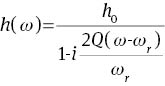
where h0 is the on-resonance amplitude transfer function (and

The RF transfer function S21,RR-OADM defined by

where Pout is the power outgoing from the RR-OADM, is then given by


where τa is, as previously, the 1/e decay time of the optical amplitude inside the cavity due to waveguide and coupling losses. Equation 13 takes a similar form to Eq. 5 in that the modulation frequency dependent denominators are identical. Figure 8 shows a comparison between experiment and model for a RR-OADM with a Q-factor of 6200. The data was obtained by modulating an optical carrier with a commercial balanced MZM operated in push-pull configuration (and thus generating symmetric sidebands) with a single tone and comparing the RF signal generated by a commercial photoreceiver receiving the modulated carrier before and after interposing the RR-OADM in between the MZM and the photoreceiver (MZM connected to the input port, photoreceiver connected to the drop port). Fiber-to-chip coupling losses were normalized out. As the Q-factor is dominated by coupling losses to the bus and add-drop waveguides, insertion losses of the critically coupled RR-OADM are low for zero optical carrier detuning (0.85 dB).
It can be seen from Eq. 13 that the -3 dBe RF bandwidth of the RR-OADM is 1/τa=f/2Q for zero detuning. Both insertion losses and RF bandwidth increase with optical carrier detuning.
An important aspect of this analysis is that the (linear scale) S21 parameters of the RRM and RR-OADM cannot, in general, be simply multiplied with each other as would be the case in a baseband RF system, as the underlying structure of the optical signal plays a significant role. Indeed, while the RF transfer function S21,RR-OADM given by Eq. 13 is accurate when the incoming optical signal has symmetric sidebands generated by a balanced MZM operated in push-pull configuration, this is not the case for the asymmetric sidebands generated by a RRM [38]. In this case, the optical amplitude transfer function of the RR-OADM, h(ω), has to be individually applied to the sidebands and the RF signal at the drop port of the RR-OADM derived from the result

where τa=2Qa/ωa and ωa are, respectively, the 1/e decay time of the E-field and the angular resonance frequency of the RRM and τb=2Qb/ωb and ωb are the equivalent quantities for the RR-OADM.
In particular, the E/O S21-parameter of the combined system looks quite different depending on whether the RR-OADM and the RRM are operated with the same or opposite carrier detuning. While in the first case peaking is very pronounced, as the effects of both devices cumulate, in the second case, the peaking effects cancel out. Figure 9A shows an example of a RRM cascaded with a RR-OADM for the case of equal and opposite detuning, with Qa=Qb=4887,

(A) Modeled E/O S21 of a RRM cascaded with a RR-OADM for equal and opposite detuning, with assumed device characteristics described in the text. While changing the sign of the RR-OADM detuning does not change its standalone S21, the compound S21 of the RRM+RR-OADM system changes. The black dashed line shows the product of the individual device S21 characteristics, for comparison. (B) Modeled E/O S21 of a RRM cascaded with a RR-OADM with zero detuning. In this commonly used configuration, the S21 of the individual devices can be simply multiplied with each other.
In practice, however, we are typically operating the RR-OADMs with zero detuning to avoid incurring additional insertion losses. In that particular instance, the S-parameters of both devices can actually be multiplied with each other. As an example, in Figure 9B, ω0-ωa was reduced to
In summary, in Sections 2–4, we have described the passive and electro-optic devices required for the link. An optimized RRM for our link requirements has been developed and its interoperability with RR-OADMs investigated. In the following, we will focus on the active devices (SS-MLLs, Section 5, and their interoperability with a commercial SOA, Section 6) before moving on to the system experiments (Section 7).
5 Single section mode-locked lasers
For the system demonstration described in the following sections we selected a Q-Dash SS-MLL from III-V Lab with comparatively low RIN and narrow optical linewidth. An overview of these lasers’ fabrication and characteristics can be found in [7–9]. The buried ridge stripe Fabry-Perot laser’s gain material consists of six stacked layers of InAs Q-Dashes in an InGaAsP barrier (DBAR) grown on an InP wafer. The stripe width is 1.25 μm. The coupling facet features a mode matching inverse taper for improved fiber coupling. The FSR of the laser is 60.8 GHz, and the center wavelength of the emitted comb is λ=1543 nm at 30°C and 300 mA injection current (with the exception of the data shown in Figure 10, the SS-MLL was operated at 30°C for all the data reported in Sections 5–7).

RF beat note spectrum as a function of injection current at four different temperatures. It is apparent that the current ranges resulting in stable mode locking are very sensitive to temperature.
The SS-MLL was eutectically soldered onto a ceramic submount that was further placed on a metal base thermally stabilized to better than 10 mK. A box covered the assembly on a vibration-damped table to protect it from air turbulence and vibrations. Constant current is supplied by shielded needle probes. A parallel capacitor close to the laser suppresses current noise. Light is coupled from the laser to a lensed polarization maintaining (PM) fiber with a 2.5 μm spot diameter. The fiber is outfitted with an antireflective coating deposited on the lensed fiber tip and is followed by a 60 dB isolator to minimize back reflections and prevent optical injection.
A closeup view of the laser die coupled to a lensed fiber and the associated spectrum can be seen in Figure 11. The lasing threshold is 13 mA at 30°C. At 300 mA, the total fiber coupled output power after the isolator is 8.3 dBm, and the power of the highest power comb line is -5 dBm. As can be seen in Figure 11B, the spectrum is flattop with 25 lines above half of the peak power per line spanning 11.6 nm of the spectrum. An important feature of SS-MLLs is that flattop power spectra are usually obtained, facilitating their use for WDM communication systems for which a minimum optical power level per channel has to be guaranteed. Mode locking in SS-MLLs is generally assumed to occur via third-order nonlinear effects [7, 8, 54, 55], and can, e.g., also be seen in frequency combs generated via nonlinear effects in microcavities in which octave-spanning spectra have been demonstrated [56]. In SS-MLLs, compensation of the linear dispersion is attributed to counteracting nonlinear dispersion arising from the gain medium and results in the phase offset of comb lines evolving with a parabolic dependency as a function of comb line wavelength [7, 8, 57]. Mode locking between the comb lines suppresses partition noise, i.e., exchange of energy between the lasing Fabry-Perot resonances due to gain competition that gives rise to high RIN when a single line of a conventional Fabry-Perot laser is isolated [58]. Partition noise prevents the utilization of conventional Fabry-Perot lasers as WDM light sources. While the RIN of isolated comb lines of SS-MLLs remains higher than the RIN of the entire comb, partition noise is sufficiently suppressed in order to enable a high-speed communication link as described in Section 7. As will be shown in the following, linewidths as low as 2.7 MHz full width at half maximum (FWHM) are measured in regions of stable operation.

(A) Detailed view of the laser coupling setup and (B) the spectrum of the SS-MLL at 30°C and 300 mA measured with a filter bandwidth of 6.4 GHz.
An additional performance metric that is specifically related to optical combs is the RF linewidth [59], i.e., the linewidth of the beat tone seen on an electrical spectrum analyzer (ESA) (PXA Signal Analyzer, Agilent Technologies, Santa Clara, USA) when the entire spectrum of the SS-MLL is sent to a photoreceiver (the full test methodology is described in the appendix). This RF line results from the beating between adjacent comb lines and has a frequency corresponding to the FSR of the laser. The width of the line is a metric for the strength and stability of the mode locking: for strong and stable mode locking, the line should be a narrowband peak. The actual width is a result of the relative phase noise between adjacent optical lines (i.e., the noise seen in the difference between the phase of adjacent lines) as opposed to the phase noise of the lines, themselves, that determines the optical linewidth.
5.1 Operating regimes
We characterized in detail the RIN, optical linewidth, and RF linewidth of the selected SS-MLL (Figure 12). The performance of a short distance OOK system is largely influenced by the RIN of the optical carrier. Optical linewidth as well as RF linewidth, on the other hand, have a minor direct impact (the transmission distance explored in Section 7 is too short to be dispersion limited given the measured optical linewidths). However, the RF linewidth, in particular, is a good indicator for the laser dynamics that also impact the RIN. In particular, it has been shown that competing supermodes with slightly different FSRs can lead to instabilities in SS-MLLs [18, 60]. Possible operating regimes can, for example, consist of a stable narrow RF line with a linewidth as low as a few tens of kHz [7, 8] (indicating a stable supermode with a well-defined FSR and strong mode locking), transition regions between two dominant supermodes (i.e., the FSR and, thus, the frequency of the RF peak suddenly jump for small environmental changes or due to noise), and even regions where two supermodes coexist, as evidenced by the coexistence of two RF lines in the RF spectrum (Figure 13).

(A) RF beat note spectrum as a function of injection current, (B) optical spectrum of an isolated line (located at λ=1537.5 nm at 300 mA) measured with a high-resolution OSA as a function of injection current, and (C) the spectrum of the entire comb’s RIN as a function of injection current. Data was taken at 30°C. In (B), the x-axis indicates the frequency offset from the expected comb line frequency as predicted from the global fit described in the text. Six instability regions are marked by red arrows (regions 1–6), and two regions with stable mode locking are marked in green (regions 7 and 8).

RF beat note spectrum at four different operating currents. Two distinct supermodes with FSR separated by 5.1 MHz can be observed at 275 mA; a narrow Lorentzian shape is featured at 250 mA and 300 mA, indicating stable mode locking. Data was taken at 30°C with a RBW of 20 kHz.
The dependence on the injection current I of the frequency f0 of a central comb line was fitted with a second-order polynomial as 195.2 THz – 502.9 MHz/mA×I – 783.2 kHz/mA2×I2. This smoothed current dependence was subtracted from the x-axis of Figure 12B before plotting, i.e., the x-axis shows the frequency offset from the expected frequency based on the global fit. The optical linewidth appears to be more broadband than is actually the case in regions 7 and 8 due to a fast modulation of the line’s frequency as can be seen in the inset. However, a Lorentzian fit reveals that the linewidth at a selected point is around 30 MHz and is limited by the optical spectrum analyzer’s (OSA) resolution. Several instability regions in the RF beat note characteristic of the SS-MLL have been marked in Figure 12A: in regions 1, 2, and 3, the beat note is completely smeared out, and the laser is not stably mode locking. Region 5 consists in a transition between two stability regions, respectively, corresponding to different dominant supermodes, so that frequent hopping between the two modi of operation is expected to occur. In region 6, two supermodes are seen to coexist. It is clearly apparent in Figure 12B and C that the RIN of the entire comb (i.e., measured without filtering out an individual line) as well as the optical linewidth of the investigated line significantly worsen in the regions of instability. The RIN of the entire comb was measured for Figure 12C to circumvent the difficulty of having a tunable optical filter track the current dependence of the comb line frequency for the large quantity of collected data. RIN data for isolated comb lines as well as optical linewidths characterized with a heterodyne measurement will be reported in the following.
Figure 13 shows detailed spectra of the RF beat note exemplifying the three regimes of operation described above. Both at 250 and at 300 mA, a relatively clean RF line can be seen (corresponding to stability regions 7 and 8 in Figure 12A), indicating mode locking, albeit the RF linewidth is significantly better at 300 mA. In between, at 275 mA, two RF lines coexist with a frequency difference of 5.1 MHz – the difference in FSR of two coexisting supermodes (instability region 6). The 225 mA is chosen in a transition region where one supermode transitions to another as the current is modified (instability region 5). The RF line is correspondingly wide.
While the diagram shown in Figure 12A was remeasured in 3 days interval with repeatable results (compare to Figure 10B), it is very temperature sensitive as can be seen in Figure 10. Nonetheless, at a stabilized temperature, large current ranges can be found for which the RF line is narrow, for example, in Figure 12A, between 228 and 257 mA.
While this data indicates that work remains to be done to make these lasers stable over a wider current and temperature window, the performance shown for well-chosen operating points is promising and is compatible with high data rate OOK WDM systems as shown in Section 7. Currently, a detailed and finely resolved study of the laser dynamics is necessary to find an appropriate operating point. Especially, the observation of the RF tone yields significant information.
5.2 Relative intensity noise
We determined the power spectral density (PSD) of the RIN for isolated comb lines in the RF frequency range from 100 kHz to 20 GHz, the result for the line at λ=1546.7 nm, which is also used for the detailed signal Q-factor system characterization shown in Section 7, being exemplarily shown in Figure 14A and discussed below. The peak in the low-frequency RIN between 100 kHz and 7 MHz, with a PSD as high as -95 dBc/Hz well above the RIN levels in the rest of the spectrum, results from power-dependent receiver noise that we were not able to reliably normalize out. For this reason, we are primarily reporting aggregate RIN numbers integrated starting from 5 MHz upward in the following in order to exclude this low-frequency measurement artifact.

(A) PSD of the RIN of an isolated comb line at λ=1546.7 nm measured between 100 kHz and 20 GHz and (B) corresponding cumulative RIN. The cumulative RIN is integrated between 100 kHz and an upper bound indicated by the x-axis. The measurement was done at 30°C and 300 mA.
Figure 14B shows the cumulative RIN for the same comb line starting at 100 kHz and integrated up to the frequency indicated on the x-axis. The initial increase corresponds to the low-speed RIN, the second increase to the more broadband RIN observed up into the few GHz range. Above 7 MHz, the RIN stays below -120 dBc/Hz and quickly drops below -140 dBc/Hz at frequencies above 4 GHz. After subtracting the noise floor of the measurement system, the noise above 4 GHz stabilizes close to the shot noise limit (shown by the red line), indicating that the laser RIN is indeed shot noise limited in this range. Integrating the RIN from 100 kHz to 20 GHz yields an aggregate RIN of 2e-3, while excluding the low speed RIN by integrating from 5 MHz to 20 GHz results in 0.8e-3 (note that these numbers still correspond to
Figure 15 shows a summary of the aggregate RIN integrated between 5 MHz and 20 GHz for each of the 20 adjacent comb lines in the flattop region of the spectrum. Figure 15A shows the data as a function of the comb line wavelength, and Figure 15B shows the data as a function of the optical power of the comb lines (as coupled to the lensed fiber). The green circle indicates the comb line that was used for the detailed signal Q-factor system characterization reported in Section 7, the SOA excess noise characterization shown in Figures 16 and 17, as well as the dependence of the isolated comb line RIN on injection current shown in Figure 18B.

Aggregate RIN (5 MHz to 20 GHz) for isolated comb lines. In (A), the data is organized by comb line wavelength, in (B) it is plotted as a function of the associated optical power. Measurements were taken at 30°C and 300 mA.

(A) Aggregate RIN of a single comb line after amplification of the entire comb by the SOA (green dots) and comparison to a model assuming a SOA NF of 6.7 dBe and an aggregate laser RIN of 1.4e-3 (black line). The data is plotted as a function of the entire power entering the SOA, and the RIN is integrated from 5 MHz to 20 GHz. The comb line at λ=1546.7 nm was isolated after the SOA to obtain this dataset. The power of the comb line lies 13.6 dB below the power of the entire comb. (B) SOA gain as a function of total input power at λ=1545.2 nm measured with a tunable laser (ASE was filtered out to calculate the gain).

Comparison of SS-MLL RIN before (black curve) and after (red curve) SOA reamplification. The latter corresponds to the highest input power data point in Figure 16A, where the aggregate RIN is very close to its asymptotic value for high SOA input power levels and ASE does not play a significant role. The excess RIN generated by the SOA, obtained as the difference of these two curves, is also shown.

(A) Aggregate RIN of the entire comb, as integrated from 8 to 300 MHz, as a function of injection current. Instability regions are labeled according to the numbering from Figure 12. (B) Detailed view of the aggregate RIN of the entire comb as integrated from 8 to 300 MHz and overlay with the aggregate RIN of an isolated comb line (λ=1546.7 nm) as integrated from 5 MHz to 20 GHz. Measurements were done at 30°C. The data for the isolated comb line appears to be shifted by 5 mA injection current relative to the data for the entire comb, which we attribute to a slight temperature drift in between measurements.
The RIN for comb lines toward the long wavelength side, around 1550 nm and above, is higher, which coincides with the upper limit of the flattop portion of the comb spectrum at 1550 nm (see optical spectrum in Figure 11B). The same effect applies to the short wavelength end of the comb, which is not included in Figure 15.
The red circle indicates an outlier in the dataset, in that the measured RIN for this comb line is significantly larger than for the rest of the lines in the flattop region (by approximately a factor 2 compared to the second worst line) and the optical power slightly lower (approximately -1 dB compared to the second worst line). Repeated measurements have proven this measurement to be reliable. This outlier may too be related to competing supermodes [18, 61]. While these datasets were taken with 300 mA at 30°C, where the RF linewidth is small and indicates strong and stable mode locking (Figures 12 and 13), the dominant supermode and a parasitic supermode may happen to have very close lines at this specific wavelength (Vernier effect), facilitating mode hopping and locally enhancing the RIN for this specific line. Without further investigations, this explanation remains, however, speculative.
Finally, we measured the aggregate RIN for a single comb line as a function of injection current, as shown in Figure 18B. While the RIN changes with current, it remains low in a 30 mA wide current window between 233 and 262 mA and acceptably low up to the highest applied current of 300 mA. Assuming the extinction ratio of 12.8 dB from the system demonstration in Section 7, the worst measured aggregate RIN in that current range, 4e-3 as integrated from 5 MHz to 20 GHz, limits the signal Q-factor to 14 (26 if corrected for the 11 GHz receiver bandwidth used in Section 7), well above the targeted signal Q-factor of 7. Incidentally, the increased RIN around 220 mA and in between 260 and 290 mA, as well as the reduced RIN region between 233 and 262 mA coincide with features of the RF beat note spectrum as seen in Figures 12 and 13 (instability regions 5 and 6, as well as stability region 7). Systematic data recorded for the RIN of the entire comb features similar trends (overlay in Figure 18B). We also investigated different fiber coupling positions in order to investigate the effect on RIN of reflections from the lensed fiber tip. Both axial as well as transversal displacements (corresponding to reduction of the coupling efficiency of, respectively, 1.5 and 0.6 dB) resulted in aggregate RIN variations under 10%.
5.3 Optical linewidth
The optical linewidth was measured with two methods: measurement with a high resolution OSA from APEX Technologies (AP2441B, Marcoussis, France) with a nominal spectral resolution of 20 MHz (Figure 12B), as well as measurement with an ESA after heterodyne down conversion by mixing with a narrow linewidth tunable laser and detection with a broadband photoreceiver. OSA measurements (Figure 11B) confirmed a FSR of 60.8 GHz and showed that the ASE emission is lower than -143 dBc/Hz (normalized relative to the power of the closest comb lines) in the flattop region of the comb. The lines drift with a rate of 7.67 pm/mA at 300 mA due to local heating of the laser die when more current is applied. However, the spectral resolution of the OSA (20 MHz) was not sufficient to resolve the optical linewidth. The complementary heterodyne linewidth measurements shown in Figure 19A revealed a linewidth of 6.2 MHz for a central line at λ=1543.86 nm, 300 mA injection current and 30°C. The linewidth at 250 mA and 30°C is nominally 2.7 MHz, but shows side lobes. This becomes even more visible at a current of 200 mA (instability region 4). For this reason, the bias point at 300 mA seems particularly adequate for system experiments, as the optical linewidth is not only relatively narrow but also features an almost pure Lorentzian line shape indicative of the absence of spurious mode hops.

(A) Optical spectrum measured with an ESA after heterodyne down conversion for three different injection currents (power levels are not normalized) recorded with a resolution bandwidth of 3 MHz. (B) Optical linewidth extracted from the heterodyne measurements as a function of injection current. The line at λ=1543.86 nm was isolated to measure this dataset. Measurements were done at 30°C.
Figure 19B summarizes the optical linewidth for various operating currents from 50 mA to 300 mA. The FWHM differs at some points from the width obtained by fitting a Lorentzian model, which is due to the strong side lobes occurring at these injection current levels.
Finally, as we have systematic optical linewidth data, we can compare it to the RF linewidth. It is apparent that the linewidth is very large for the current range between 250 and 300 mA for which two supermodes coexist, as well as below 100 mA for which the RF line is completely smeared out and the laser is not stably mode locking. This correlation can also be seen in Figure 12 by comparing the optical linewidth measured with the APEX OSA (Figure 12B) to the measured RF linewidth (Figure 12A).
Based on the characterization data shown in this section, we chose to operate the SS-MLL at 30°C and 300 mA injection current for the system characterization.
6 Semiconductor optical amplifier
Even though the link demonstrations shown in Section 7 are based on amplification with an EDFA, we are targeting a final architecture using a SOA due to its compactness and its potential for lower-cost solutions. Moreover, the center wavelength of a SOA gain spectrum is more flexible and can more easily be matched to the SS-MLL. However, its limited maximum output power, higher noise figure (NF) penalized due to higher chip coupling losses, and the requirement to operate in the linear regime when reamplifying a data stream (due to the short time constants of SOA carrier dynamics [62]) create additional challenges. An important aspect is the effect of SOA amplification on the RIN of a semiconductor mode-locked laser. In [20], a single comb line of a SS-MLL was amplified prior to modulation by a SOA operated in deep saturation, not only maintaining the RIN level, but actually substantially improving it. We are, however, targeting joint reamplification with a single device of all the WDM communication channels after modulation and incurring the insertion losses of the RRMs (amplification before the RRMs would be less effective due to the output power limitation of the SOA), so that neither prefiltering of single comb lines nor operating the device in deep saturation are an option. As the entire comb is reamplified, this raises the question whether nonlinear interaction between the comb lines, for example, via four-wave mixing (FWM) and cross gain modulation (XGM), impacts the RIN. Results relating to the reamplification with a single SOA of an entire InGaAs mode-locked laser spectrum centered on 1310 nm have already been reported in [63], where it was shown that reamplification of an entire comb with a quantum dot SOA was possible without generating excess RIN. Here, we systematically investigate the RIN of our C-band SS-MLL reamplified with a commercial quantum well SOA (Thorlabs S9FC1004P Booster Optical Amplifier, Thorlabs Inc., NJ, USA) with a measured saturated output power of 13.4 dBm at 1545.2 nm after ASE filtering (defined as the output power at the 3 dB gain compression point).
Figure 16 shows the measured RIN of an isolated comb line after SOA amplification of the entire SS-MLL spectrum. The power entering the SOA is controlled by an attenuator. After the SOA (and additional attenuation to prevent exceeding the maximum power rating of downstream devices), a tunable optical filter with a 40 GHz pass band is used to filter out a single comb line, which is then sent to a Finisar 40 GHz bandwidth XPRV2021A photoreceiver followed by an ESA. The RIN PSD was integrated in the range from 5 MHz to 20 GHz to obtain the aggregate RIN.
At low SOA input power levels, the RIN is clearly dominated by ASE, as shown by consistency with the NF specified for the SOA. A detailed inspection of the RIN spectrum also shows that the excess noise generated by transmission through the SOA is broadband in nature at low SOA input powers, as would be expected from ASE. However, comb lines isolated after amplification also feature a moderate excess RIN penalty in addition to ASE visible at high SOA input power levels: the aggregate RIN of isolated comb lines reaches an asymptotic value at high SOA input power levels that lies above the RIN measured from the same comb line prior to amplification.
The measured RIN is highly dependent on the SOA input power and can be described very well by ASE corresponding to a fitted SOA NF of 6.7 dBe (very close to the 7 dBe specified as typical by the manufacturer) in addition to a power-independent aggregate RIN (5 MHz to 20 GHz) of 1.4e-3 (the asymptotic value of the curve at high SOA input power levels). While this additive term, 1.4e-3 is higher than the RIN measured directly from the same comb line without SOA amplification, 0.8e-3 as reported in Section 5, it is expected to still be sufficiently low to allow 14 Gbps link performance with a signal Q-factor exceeding 7 (see red curve in Figure 20A).

(A) Signal Q-factor as a function of average power reaching the photoreceiver for a single SS-MLL comb line (blue dots) and an Agilent bench-top laser (black dots). Measurement results (dots) are compared to a basic noise model (lines). A model incorporating the higher NF of the SOA as well as the excess non-ASE RIN generated by the SOA is also included (red line). (B) ‘0’- and ‘1’ level noise as extracted from recorded eye diagrams (circles and dots) and as modeled (doted and continuous curves).
The spectra of the comb line RIN prior to amplification, after amplification in the high SOA input power regime (low ASE, but SOA saturation), and the difference between the RIN spectra are shown in Figure 17. Figure 16B shows that the SOA leaves the linear regime at around -10 dBm total input power and reaches 3 dB gain compression at -3 dBm input power. In a separate experiment, we were also able to reduce the RIN by amplification of a single comb line with the commercial SOA, so that the excess RIN observed here is definitely a consequence of nonlinear interaction between the comb lines inside the SOA. While the excess RIN may be related to SOA saturation and increased XGM or FWM, it is not yet clear whether it will also be incurred in the linear SOA operation regime, so that we are including the excess RIN in the system analysis of the next section. As already mentioned, there are examples in the literature of amplification of a quantum dot MLL with a SOA relying on the same gain material without increase of the RIN [63], so the excess RIN observed here could be related to the quantum well gain medium of the commercial SOA.
7 Link demonstrator
In order to demonstrate the suitability of the SS-MLL investigated here (Section 5) for high-speed WDM transceivers, we recorded eye diagrams for multiple comb lines at 14 Gbps after modulation with a RRM followed by individual reamplification with an EDFA and extracted the signal Q-factors. In particular, these measurements show that the laser RIN of the selected SS-MLL is adequate for high-speed communications.
To evaluate the Tx performance, we used the setup shown in Figure 21 consisting in the 60.8 GHz FSR SS-MLL described in Section 5, operated at 300 mA and 30°C and resulting in -5 dBm coupled into the lensed fiber for the best comb line (-5.3 dBm for the comb line at λ=1546.7 nm used for the detailed signal Q-factor analysis shown in Figure 20), followed by the third category 10 μm radius RRM described in Section 2 (with a FSR of 10 nm). The light is coupled from the laser into a lensed fiber, sent through an isolator, and then coupled into the SiP chip with a grating coupler (the grating couplers have 5.2 dB insertion losses and were not particularly carefully optimized in this first generation of demonstrator). After modulation, the signal is again grating coupled to a fiber adding another 5.2 dB coupling loss. Based on the measured RRM extinction ratio of 12.8 dB obtained after optimizing the carrier detuning for highest signal Q-factor, we estimate with our models P1 and P0, defined as the power transmitted through the RRM bus waveguide in the ‘1’ and ‘0’ states, to be, respectively, -7.4 dB and -20.2 dB below the incoming power in the bus waveguide. While the normalized OMA of -7.6 dB is below the -6.4 dB attainable with this RRM, the higher extinction resulting from a smaller detuning improves tolerance to RIN and ASE. Owing to the reduced detuning, the measured E/O bandwidth of the device is also reduced from 29 GHz to 19 GHz.

Diagram of the characterization setup (PPG, programmable pattern generator; PC, polarization controller; VOA, variable optical attenuator; Rx, photoreceiver).
The thermal tuner of the RRM was current driven and manually controlled by a Keithley Source Meter (Keithley Instruments, Solon, USA), while the data stream was generated by a programmable pattern generator (PPG) from Anritsu (Atsugi, Japan) (MU183020A 28G/32Gbps PPG) as a PRBS-7 pseudorandom bit sequence. After the RRM, the channel is filtered by a C-band tunable optical filter with a 40 GHz pass band and additional 2.1 dB insertion losses. The initial goal was to filter out a group of eight or 12 channels, but being short of a filter with the necessary pass band, we opted for characterizing the channels one by one, demonstrating the basic suitability of the SS-MLL in combination with a SiP RRM. The filter is followed by a high-power EDFA from Amonics (Hong Kong). For the comb line at λ=1546.7 nm, the signal levels entering the EDFA are -25.2 dBm for the ‘1’ level and -38.0 dBm for the ‘0’ level. The saturated EDFA output power is 13 dBm average power. After the EDFA, the average power is attenuated to 4 dBm (including the insertion losses of the following filter), in order to avoid exceeding the power rating of downstream devices and again filtered for ASE noise reduction, reducing the average power by another 4.9 dB corresponding to ASE. After reception by a Finisar 40 GHz photoreceiver, the eye diagram was visualized by an Agilent DSA-X 920048 real-time oscilloscope.
The combined -3 dBe cutoff frequency of the RF cables and of the photoreceiver is measured to be above 20 GHz, so that it does not limit the opening of the measured eye diagrams. The analog front end of the oscilloscope recording the eye diagrams was set to 11 GHz for noise reduction.
The SS-MLL outputs 17 lines with power levels between -7 dBm and -5 dBm per line as measured in the lensed fiber, with said lines adjacent to each other but for a single outlier in their midst with only -7.8 dBm coupled power. This is also the outlier flagged as having high RIN in Section 5 (circled in red in Figure 15). We used the same RRM to sequentially measure the eye diagram for each of these comb lines. As FOM, we use the signal Q-factor of the channels defined as:

where P1-P0 is the vertical eye opening visualized on the oscilloscope, and σ1 and σ0 are the standard deviations of the noise for the ‘1’ and ‘0’ symbols (the methodology for determining the Q-factors is described later in this section). The 18 channels achieved signal Q-factors of more than 4.7, with half of them achieving signal Q-factors of more than 7 corresponding to a bit error rate (BER) of better than 1×10-12. Figure 22A shows the Q-factor over all the 18 adjacent channels (the outlier is the fifth from the left). Figure 22B shows an example of a recorded eye diagram.

(A) From top to bottom: recorded signal Q-factors, optical power per comb line as coupled into the lensed fiber and EDFA saturated output power as a function of wavelength. It can be seen that the signal Q-factors strongly correlate with the latter two. Because of the limited tuning range, the points in red were measured with a second RRM corresponding to the same design, but with a different resonance wavelength, explaining the local deviation from the global trend. (B) Example of a recorded eye diagram corresponding to the comb line at λ=1546.7 nm.
The graph also shows the power per comb line coupled into the lensed fiber as well as the wavelength-dependent saturation output power of the EDFA. It is apparent that the Q-factors strongly correlate to the comb line power (not surprisingly based on the data in the next paragraph showing that noise is dominated by ASE generated by the EDFA) as well as to the saturation power of the EDFA (the NF also increases at shorter wavelengths according to the datasheet). The lower-signal Q-factors are associated to comb lines with low initial power and to the wavelength region with reduced EDFA output power and increased NF.
In order to verify the main factors limiting the signal Q-factor, we measured it for one line (λ=1546.7 nm) as a function of the power reaching the photoreceiver, by varying the attenuation between the EDFA output and the photoreceiver. We repeated the measurement with an Agilent bench-top tunable laser (Agilent tunable laser source 81600B) in order to characterize the excess noise generated by the SS-MLL. The Agilent laser power was chosen so that the power launched into the fiber matched that of the SS-MLL. The recorded Q-factors are plotted as a function of the average power reaching the photoreceiver in Figure 20A.
To obtain the Q-factors from the recorded eye diagrams, we exported the data and applied a more complex data processing in order to clearly separate the modulation penalty arising from intersymbol interference (ISI) and random noise arising from ASE, Rx noise, and laser RIN. We averaged 120 full PRBS-7 sequences to obtain an eye diagram with reduced noise allowing a clear identification of the reduction of the vertical eye opening due to ISI (the ISI penalty). An unprocessed eye diagram and an eye diagram averaged over the data pattern are shown in Figure 23. We extracted an ISI penalty of 1 dB reduction of the vertical eye opening independently of the laser source and of the power attenuation between the EDFA and the photoreceiver. The difference between the recorded trace and the average trace was then extracted in order to analyze the noise. Noise distributions for both the ‘0’ and ‘1’ levels feature the expected Gaussian dependencies (Figure 23C and D). The extracted noise standard deviations for both laser sources are summarized in Figure 20B. The Q-factors of the eye diagrams were then calculated by plugging the vertical opening of the averaged eye diagrams as P1-P0 in Eq. 15 and by plugging in the extracted noise standard deviations in the denominator.

(A) Example of unprocessed eye diagram after EDFA amplification (-2.9 dBm average input power to the photoreceiver with SS-MLL comb line as a light source). (B) Eye diagram after averaging of 120 PRBS-7 traces. The remaining eye closure is attributed to ISI and corresponds to a 1-dB penalty. (C) Histogram of the noise distribution of the ‘0’-level and (D) histogram of the noise distribution of the ‘1’-level. It should be noted that the electrical eye diagrams (A) and (B) are inverted, as the photoreceiver has an inverting amplifier.
The data was modeled with the following equation in which Rx noise, RIN, and ASE are included in the ‘1’ and ‘0’ level noise standard deviations and are added as sum-of-squares

where P1,Rx and P0,Rx are, respectively, the ‘1’ and ‘0’ bit power levels at the input of the photoreceiver, Pn,Rx is the input referred noise of the photoreceiver in W·Hz-0.5, F is the noise factor of the EDFA, F=10NF/10, h is Planck’s constant, f0 is the optical carrier frequency, P1,EDFA and P0,EDFA are the ‘1’ and ‘0’ power levels at the input of the EDFA, BW=11 GHz is the equivalent noise bandwidth of the Rx including the analog front end of the oscilloscope (as the oscilloscope has a steep roll-off, the equivalent noise bandwidth is very close to the -3 dBe roll-off), and RINt is the aggregate RIN (on a linear scale). G is the total gain between the input of the EDFA and the input of the photo-receiver and η is the eye closure penalty due to ISI occurring after the photo-receiver. The reduction of the extinction due to ISI is taken into account in the optical power levels P0,EDFA and P0,Rx in the denominator of Eq. 16 in order to properly model the ‘0’-level noise (note that the effect of ISI on the ASE noise levels is different depending on whether the signal distortion occurs before or after conversion into the electrical domain – here, we lumped everything into the optical domain by simply adjusting P0,EDFA and P0,Rx, as the discrepancy turned out to be a slight one).
The RIN term (RINt=0.8e-3) is only included in the curve modeling the signal Q-factor generated with the SS-MLL as a light source, under the assumption that RIN is negligible in the eye diagrams recorded with the bench-top laser (specified as less than -145 dBc/Hz above 0.1 GHz). The EDFA NF was independently measured as 6 dBe. The input-referred amplifier noise in the Rx is set to 40 pA/Hz0.5 in accordance to the datasheet of the manufacturer, resulting in 53 pW/Hz0.5 input referred to the optical domain assuming a worst-case photodetector responsivity of 0.75 A/W also specified by the manufacturer. As described above, the penalty to the OMA due to ISI was extracted as -1 dB from the eye diagrams, and the optical power levels entering the EDFA were estimated as -25.2 dBm and -38 dBm for the ‘1’ and ‘0’ levels, respectively. While the ISI distortion is already explicitly taken into account by η in the numerator, in the denominator, the ISI distortion was taken into account by adjusting the optical power levels P0,EDFA and P0,Rx.
The comparison between the data extracted from the eye diagram measurements and the model can be seen in Figure 20, with quite good agreement given that there remain no free parameters in the model. A third curve in Figure 20A also shows the Q-factor that would be expected after replacing the EDFA with the commercial SOA characterized above, given its increased NF (6.7 dBe) and the excess RIN (1.4e-3 vs. 0.8e-3) generated by the SOA.
While the channels were measured one by one by retuning the RRM in this first demonstration, in the envisioned system architecture, several RRMs will be simply cascaded one after the other along a single bus waveguide. As RRMs have very little effect on optical carriers outside of their resonance linewidth (with excess losses below our current measurement repeatability gauge), small excess losses are expected from the latter.
A number of conclusions can be drawn from this analysis: most importantly, at equal EDFA input power, the SS-MLL comb line performs almost as good as the instrument-grade bench-top laser. We can set the Rx noise to zero in the model in order to calculate the signal Q-factor limited by laser noise and ASE only (this corresponds to the asymptotic value of the curves at very high Rx input power). This results in a maximum signal Q-factor of 8.2 for the SS-MLL comb line vs. 8.9 for the bench-top laser, further indicating that the excess penalty introduced by the SS-MLL at equal EDFA input power is very small. This asymptotic value is estimated to 7.4 if the SS-MLL was reamplified by the SOA rather than by the EDFA. While a Q-factor of 7 can still be reached according to this model, the margin is very small so that the input power to the optical amplifier is close to the minimum required and can, thus, be used to derive bounds on required comb line power and grating coupler/RRM efficiencies. Given the amplifier input power used here, the minimum average Rx input power levels to maintain a Q-factor of 7 are, respectively, -10.2 dBm, -9.4 dBm, and -7.2 dBm for the EDFA reamplification of the Agilent laser, the EDFA reamplification of the SS-MLL line and SOA reamplification of the entire comb. This last number can be used to estimate the required SOA output saturation power required to sustain a given number of WDM channels.
As the RRM is used here at an operating point with a -3 dBe O/E bandwidth of 19 GHz, it should, in principle, be compatible with 25 Gbps OOK using larger FSR SS-MLLs. After increasing the Rx bandwidth (here increasing the oscilloscope bandwidth throttling the link), this would, however, require a 25/14∼1.8 times increase in the EDFA input power per channel to maintain the same ASE limited Q-factor. By removing the intermediate fiber between the laser and the SiP chip [64, 65], and thus removing an optical interface, and by improving the grating coupler losses, this power level can be reached. Moreover, SS-MLLs with a slightly larger FSR are also expected to emit more power per comb line (the optimum in this regard is for a FSR on the order of 70–100 GHz, above 100 GHz, the power per comb line drops again due to the decreased cavity size). Finally, placing the SOA on-chip before the second grating coupler would remove one more optical interface prior to optical amplification.
The channel count, on the other hand, will be limited by the saturation output power of the SOA. Based on the analysis done above, a minimum average power of -7.2 dBm is required at the Rx (before internal fiber coupling losses) for SOA-based 14 Gbps operation. Integrating germanium waveguide photodetectors [66] in the same SiP chip as the RR-OADMs would remove two optical interfaces in the WDM Rx; however, the link budget would still need to accommodate an interface between the SOA and the Tx SiP chip, a single polarization grating coupler between the Tx chip and the fiber, a polarization splitting grating coupler between the fiber and the Rx, the insertion losses of the RR-OADMs, and excess losses due to on-chip waveguides, the total of which is estimated to be on the order of 13 dB losses after the SOA. The additional OMA required for compensating the increased noise resulting from increasing the data rate from 14 to 25 Gbps (approximately 1.3 dB assuming dethrottling the receiver to a 20-GHz bandwidth) can be provided by transitioning to an integrated germanium photodetector without the internal optical coupling losses of the fiber-coupled commercial receiver. For eight WDM channels, the total internal output power required from the SOA chip (-7.2+13+10·log10(8)=14.8 dBm) is in line with the 13-dBm generated after fiber coupling losses by the commercial SOA investigated here at the -3 dB gain compression point (Figure 16B). Much higher 3 dB compression saturation levels of 19 dBm have been reported in the literature [67]. In order to reach the required SOA output power of -7.2+13=5.8 dBm per comb line, a small signal internal SOA gain above 27 dB is required assuming a modest 4 dB improvement to the SOA input power compared to the current setup.
A number of challenges remain to be addressed, notably developing a temperature-stabilized optical module solution with an attractive power budget, developing a practical laser integration scheme, and obtaining high laser to laser device repeatability. Efforts are under way to address these.
8 Conclusions
We demonstrated that the comb lines of Q-Dash SS-MLLs can support 14 Gbps WDM optical channels with SiP-based RRMs and reamplification with an EDFA. System characterization also indicates that the architecture should be compatible with SOAs, paving the way for a more compact and lower-cost solution. We gave a detailed overview of individual component optimization and characterization performed to support this architecture. RRMs were optimized for targeted data rates by adjusting the phase shifter dopant concentrations, the coupling strength to the bus waveguide, as well as the frequency detuning of the optical carrier relative to the resonance frequency trading off bandwidth, OMA, and extinction ratio under consideration of RIN and ASE noise. We compared three different thermal tuner architectures. The asymmetric sidebands generated by RRMs were shown to modify the S21 of downstream RR-OADMs in the general case. Moreover, we thoroughly characterized the RF linewidth, optical linewidth, and RIN of a SS-MLL and identified an operation regime conducive to the system demonstration. The SS-MLL had a FSR of 60.8 GHz and 25 comb lines with a power within 3 dB of the highest line power of -5 dBm. The RIN of isolated comb lines was on the order of -120 dBc/Hz between 10 MHz and 4 GHz, and shot noise limited above 4 GHz. We demonstrated 14 Gbps modulation for 18 adjacent comb lines and used detailed signal Q-factor characterization to extrapolate link budgets in view of higher data rates and SOA integration. Data indicates that more than eight channels should be supported with a single SOA.
About the authors

Juliana Müller is currently a doctoral student at the Institute for Integrated Photonics of RWTH Aachen University. Her current research focuses on resonant ring modulators for WDM transceivers. From 2007 to 2013, she studied Electrical Engineering at RWTH Aachen University with a focus on micro- and nano-electronics. She received her Master’s degree in 2013.

Johannes Hauck is a doctoral student at the Institute for Integrated Photonics of RWTH Aachen University. The focus of his current research lies with silicon photonic systems with a particular emphasis on coherent wavelength division multiplexed transceivers. From 2005 to 2011, he studied Physics at RWTH Aachen University with focus on optical systems, laser technology, extreme-ultraviolet optics and solid-state physics. He received his Dipl.-Phys. degree from RWTH Aachen University in 2011.

Bin Shen received his BSc in Material Science and Engineering from the Zhejiang University of Technology (China) with a focus on Polymer Science in 2008 and his MSc in Material Science with a focus on Nanotechnology and Electric Materials from RWTH Aachen University in 2012. He joined the Institute for Integrated Photonics of the RWTH Aachen in 2011 as a Master Student and is now working toward a PhD degree in Electrical Engineering. After working on test automation methodologies, the focus of his current research is on nonlinear optical devices.

Sebastian Romero-García received the Ingeniero de Telecomunicación degree from the University of Malaga, Spain, in 2009. From 2009 to 2011, he was a Research Assistant at the Department of Communications Engineering, University of Malaga. Since 2011, he has been with the Institute for Integrated Photonics of RWTH Aachen University where he is currently working toward the PhD degree in Electrical Engineering. His research interests focus on the development of integrated photonic devices and systems. Recent publications cover the development of a SiN back-end waveguide technology for biosensing, as well as the development of alignment tolerant couplers for hybrid Silicon Photonics system integration.

Elmira Islamova received a Bachelor’s degree in Telecommunications from SPbNRU ITMO (St. Petersburg, Russia) in 2013 and is now studying toward a Master’s degree in Communications Engineering at RWTH Aachen University. She is currently doing research at the Institute for Integrated Photonics with a primary focus on the characterization of integrated silicon ring-resonator modulators and add-drop multiplexers.

Saeed Sharif Azadeh joined the Institute for Integrated Photonics of RWTH Aachen University as a PhD student in July 2012. His PhD project includes the simulation and design of silicon photonics electro-optical modulators, device fabrication, and high frequency device characterization. He received his MSc in Electrical Engineering from Sharif University of Technology (Iran) in 2011 where he investigated optical properties of HTC superconductor devices.

Siddharth Joshi received his Integrated MSc degree in Photonics from Cochin University of Science and Technology (India) in 2011 and a PhD degree in Optical Telecommunications from Université Pierre et Marie Curie (France). During his PhD as a Marie Curie early stage researcher, he worked at III–V Lab on conception and fabrication of low-chirp and low-phase noise optical sources based on quantum dash nano-structures. Presently, he is working at Institut Electronique Fondametale (France) toward the development of terahertz quantum cascade lasers.

Nicolas Chimot received the Master’s diploma in Light and Matter Interaction in 2003 from the University of Rennes I and the PhD degree in 2006 from the University of Paris XI. His PhD work was focused on the development of photoconductive emitters and detectors driven at 1550 nm for the generation of terahertz electromagnetic waves and the conception of ultrafast photo switches. From 2006 to 2008, he was a postdoctoral Researcher at Molecular Electronic Laboratory at Commissariat à l’Energie Atomique at Saclay, France. He worked on the conception of carbon nanotube-based transistors on flexible substrate for high-frequency applications and on the conception of nanoelectromechanical devices with carbon nanotubes. Since 2008, he has works at the III–V Lab, Alcatel-Lucent, in the Photonic Integrated Circuit team. He is currently involved in the optimization and characterization of QD-based lasers for telecommunication applications.

Alvaro Moscoso-Mártir received his MSc degree in Telecommunications Engineering from Málaga University (Spain) in 2008 and his PhD degree in Microwave Engineering from Málaga University in 2013. During his PhD, he focused on the design of ultra-wideband radiofrequency circuitry in integrated planar technology for six-port receivers. Currently, he is working as a Postdoctoral Scholar at the Institute for Integrated Photonics of the RWTH Aachen, where his main research activities focus on the design of microwave circuits and components and on the modeling and assembly of optoelectronic components.

Florian Merget received his Dipl.-Ing. and his PhD in Electrical Engineering from RWTH Aachen University (Germany) in 2002 and 2008. During his PhD, he worked on electrical and optical chalcogenide phase change memory devices and specialized on semiconductor fabrication technologies. In 2008, he joined the Silicon Photonics Group of the Institute of Semiconductor Electronics (led by Prof. H. Kurz) as a project manager. In 2011, he joined the newly established Silicon Photonics Laboratory as a staff scientist. His main research interests focus on complex and high-speed data transmission systems and electro-optic components that are specifically targeted to meet the needs of next-generation telecom and datacom applications.

François Lelarge received the Diploma in Material Science in 1993 and the PhD degree in 1996, both from the University of Pierre et Marie Curie, Paris, France. From 1993 to 1996, he was with the Laboratory of Microstructures and Microelectronic, CNRS Bagneux, France. His thesis work was devoted to the fabrication and the optical characterization of GaAs/AlAs lateral superlattice grown on vicinal surfaces by MBE. From 1997 to 2000, he was a postdoctoral researcher at the Institute of Micro and Optoelectronics, Lausanne, Switzerland. He worked on InGaAs/GaAs quantum wires fabrication by MOCVD regrowth on patterned substrates. Presently, he is in charge of the Epitaxy and New Material Technology team within III–V Lab and coordinator of a project on QD-based directly modulated lasers (ANR-DIQDOT). He has published more than 110 papers and communications in national and international conferences, including invited talks and postdeadline papers on QDot-based devices.

Jeremy Witzens has been leading the Institute for Integrated Photonics of the RWTH Aachen since 2011. Prior to joining the RWTH, he was a Principal Research Scientist at the University of Washington (2009–2010), a Sr. Staff Engineer at Luxtera Inc. (2006–2009), a Postdoctoral Scholar at the California Institute of Technology (2005), and an Integrated Optics Designer at Luxtera Inc. (2002–2003). He received his PhD from the California Institute of Technology in 2005, where he worked on Photonic Crystal Micro-Cavities and Photonic Crystal-based light steering devices, and his Engineering Diploma from the Ecole Polytechnique (Palaiseau, France). He has been working on Silicon Photonics since 2002, co-authored papers and co-invented patents on topics such as germanium waveguide photodetectors, silicon electro-optic modulators, WDM and add-drop multiplexers, optical fiber- and laser-to-chip couplers, and photonic-electronic integration. His current research interests include high-performance Silicon Photonics modulators, alignment-tolerant optical chip couplers, comb light sources, group IV light sources, advanced transceiver architectures, hybrid photonic integration, and biophotonics. He received an ERC award in 2011 and is currently coordinating the European project ‘Broadband Integrated and Green Photonics Interconnects for High-Performance Computing and Enterprise Solutions’ (BIG PIPES).
Appendix: SS-MLL RF linewidth measurements
The FSR and, thus, the center frequency of the RF line of the SS-MLL used for the experiments was 60.8 GHz, which is above the direct measurement capability of our 50 GHz ESA and our 40 GHz photoreceiver. Therefore, the SS-MLL’s output was amplitude modulated with a 20 GHz sine wave applied to a commercial MZM. The generated sidebands interfere with the neighboring comb lines generating a 40.8 GHz RF line and with the neighboring lines’ sidebands generating a 20.8 GHz RF line. We recorded the line at 40.8 GHz due to its larger signal strength, resulting from the fact that the generated sidebands are weaker than the carrier in our setup. For lasers with even higher FSR, the sideband-to-sideband interference (here 20.8 GHz) can be observed instead in order to increase the frequency down conversion, or higher-order sidebands can be generated by driving the MZM above its nominal drive voltage.
Acknowledgments
The authors would like to acknowledge funding by the European Commission for the project ‘Broadband Integrated and Green Photonic Interconnects for High-Performance Computing and Enterprise Systems’ (BIG PIPES) under contract number 619591 and for the project ‘Compact Silicon Photonics Coherent WDM Transceiver’ (COWDM) under contract number 293767, by the European Research Council for Project ‘Frontiers of Integrated Silicon Nanophotonics in Telecommunications’ (FISNT) under contract 279770 and by the German Federal Ministry of Science and Education (BMBF) for the project ‘Safe and Secure European Router’ (SASER) under contract 16BP12504. Chips were fabricated at IMEC in the framework of the shuttle service ePIXfab and at Singapore’s Institute of Microelectronics (IME).
Author’s contributions: J.M., J.H., and J.W. wrote the paper. J.M., J.H., and E.I. did the measurements. J.M. and S.S. performed the simulations. F.M. and S.R. designed the chips. J.M., J.H., B.S., and S.S. built the measurement setups. N.C., S.J., and F.L. developed and fabricated the lasers. J.M., J.H., and J.W. analyzed the data. J.W., F.L., F.M., and A.M. supervised the project. J.W. initiated and planned the project.
References
[1] http://www.cwdm4-msa.org.Search in Google Scholar
[2] https://www.clr4-alliance.org.Search in Google Scholar
[3] http://www.openopticsmsa.org.Search in Google Scholar
[4] A. Ghiasi, Proc. in ‘9th IEEE Int. Conf. GFP’, 27–29 (2012).Search in Google Scholar
[5] W. Mao, U. Koren, S. Rochus, E. Flynn, R. L. Hartmann, et al., in ‘Proc. 2010 IEEE MILCOM Conf.’, 875–879 (2010).Search in Google Scholar
[6] A. Akrout, A. Shen, R. Brento, F. Van Dijk, O. Legouezigou, et al., IEEE Photon. Tech. L. 21, 1746–1748 (2009).10.1109/LPT.2009.2032243Search in Google Scholar
[7] R. Rosales, K. Merghem, A. Martinez, A. Akrout, J.-P. Tourrenc, et al., IEEE J. Sel. Top. Quant. 17, 1292–1301 (2011).10.1109/JSTQE.2011.2116772Search in Google Scholar
[8] R. Rosales, S. Murdoch, R. Watts, K. Merghem, A. Martinez, et al., Opt. Express 20, 8649–8657 (2012).10.1364/OE.20.008649Search in Google Scholar PubMed
[9] F. Lelarge, B. Dagens, J. Renaudier, R. Brenot, A. Accard, et al., IEEE J. Sel. Top. Quant. 13, 111–124 (2007).Search in Google Scholar
[10] S. Joshi, C. Calo, N. Chimot, M. Radziunas, R. Arkhipov, et al., Opt. Express 22, 11254–11266 (2014).10.1364/OE.22.011254Search in Google Scholar PubMed
[11] A. Gubenko, I. Krestnikov, D. Livshtis, S. Mikhrin, A. Kovsh, et al., Electron. Lett. 43, 1430–1431 (2007).Search in Google Scholar
[12] M. Strain, P. Stolarz and M. Sorel, IEEE J. Quantum Elect. 47, 492–499 (2011).10.1109/JQE.2010.2091396Search in Google Scholar
[13] P. Del’Haye, A. Schliesser, O. Arcizet, T. Wilken, R. Holzwarth, et al., Nature 450, 1214–1217 (2007).Search in Google Scholar
[14] L. Razzari, D. Duchesne, M. Ferrera, R. Morandotti, S. Chu, et al., Nat. Photonics 4, 41–45 (2010).10.1038/nphoton.2009.236Search in Google Scholar
[15] J. Levy, A. Dondarenko, M. Foster, A. Turner-Foster, A. Gaeta, et al., Nat. Photonics 4, 37–40 (2010).10.1038/nphoton.2009.259Search in Google Scholar
[16] J. Pfeifle, V. Brasch, M. Lauermann, Y. Yu, D. Wegner, et al., Nat. Photonics 8, 375–380 (2014).10.1038/nphoton.2014.57Search in Google Scholar PubMed PubMed Central
[17] P. Anandarajah, R. Zhou, R. Maher, M. Gutierrez Pascual, F. Smyth, et al., in ‘Proc. 2013 Opt. Fiber Commun. Conf. (OFC)’, OTh3I.8 (2013).Search in Google Scholar
[18] K. Merghem, C. Calo, R. Rosales, X. Lafosse, G. Aubinet, et al., IEEE J. Quantum Elect. 50, 275–280 (2014).10.1109/JQE.2014.2308323Search in Google Scholar
[19] Y. Liu, R. Ding, Q. Li, X. Xuan, Y. Li, et al., in ‘Proc. 2014 Opt. Fiber Commun. Conf. (OFC)’, Th4G.6 (2014).Search in Google Scholar
[20] M. Gay, A. O’Hare, L. Bramerie, Z. Hao, S. Fresnel, et al., in ‘Proc. 2014 Opt. Fiber Commun. Conf. (OFC)’, Tu2H.5 (2014).Search in Google Scholar
[21] P. Delfyett, S. Gee, M. Choi, H. Izadpanah, W. Lee, et al., J. Lightwave Technol. 24, 2701–2719 (2006).10.1109/JLT.2006.875948Search in Google Scholar
[22] P. Dong, S. Liao, D. Feng, H. Liang, D. Zheng, et al., Opt. Express 17, 22484–22490 (2009).10.1364/OE.17.022484Search in Google Scholar PubMed
[23] Q. Xu, B. Schmidt, J. Shakya and M. Lipson, Opt. Express 14, 9430–9435 (2006).Search in Google Scholar
[24] A. Knights, E. Huante-Ceron, J. Ackert, D. Logan, G. Wojcik, et al., in ‘Proc. 9th IEEE Int. Conf. GFP’, 210–212 (2012).Search in Google Scholar
[25] P. Dong, W. Qian, H. Liang, R. Shafiiha, D. Feng, et al., Opt. Express 18, 20298–20304 (2010).10.1364/OE.18.020298Search in Google Scholar PubMed
[26] J. Lee, I. Shubin, J. Yao, J. Bickford, Y. Luo, et al., Opt. Express 22, 7678–7685 (2014).10.1364/OE.22.007678Search in Google Scholar PubMed
[27] B. Little, S. Chu, H. Haus, J. Foresi and J.-P. Laine, J. Lightwave Technol. 15, 998–1005 (1997).10.1109/50.588673Search in Google Scholar
[28] L. Vivien, J. Osmond, J.-M. Fedeli, D. Marris-Morini, P. Crozat, et al., Opt. Express 17, 6252–6257 (2009).10.1364/OE.17.006252Search in Google Scholar PubMed
[29] P. De Dobbelaere, B. Analui, E. Balmater, D. Guckenberger, M. Harrison, et al., Proc. 2008 Eur. Conf. Opt. Commun. (ECOC) 2, 91–92 (2008).Search in Google Scholar
[30] R. A. Soref and B. R. Bennett, IEEE J. Quantum Elect. 23, 123–129 (1987).Search in Google Scholar
[31] G. Reed, G. Mashanovich, F. Gardes and D. Thomson, Nat. Photonics 4, 518–526 (2010).10.1038/nphoton.2010.179Search in Google Scholar
[32] D. M. Gill, S. Patel, M. Rasras, K. Tu, A. White, et al., IEEE J. Sel. Top. Quant. 16, 45–52 (2010).Search in Google Scholar
[33] H. Yu, D. Ying, M. Pantouvaki, J. Van Campenhout, P. Absil, et al., Opt. Express 22, 15178–15189 (2014).10.1364/OE.22.015178Search in Google Scholar PubMed
[34] J.You, M. Park, J. Park and G. Kim, Opt. Express 16, 18340–18344 (2008).10.1364/OE.16.018340Search in Google Scholar PubMed
[35] W. D. Sacher and J. K. S. Poon, Opt. Express 20, 15741–15753 (2008).10.1364/OE.16.015741Search in Google Scholar PubMed
[36] L. Zhang, Y. Li, J. Yang, M. Song, R. Beausoleil, et al., IEEE J. Sel. Top. Quant. 16, 149–158 (2010).Search in Google Scholar
[37] J. Rhim, Y. Ban, J. Lee, S. Cho and W. Choi, in ‘Proc. 11th IEEE Int. Conf. GFP’, 7 (2014).Search in Google Scholar
[38] J. Müller, F. Merget, S. Sharif Azadeh, J. Hauck, S. Romero Garcia, et al., Sci. Rep. 4, 6310 (2014).Search in Google Scholar
[39] S. Sharif Azadeh, J. Müller, F. Merget, S. Romero-Garcia, B. Shen, et al., Proc. Soc. Photo-Opt. Ins. 9288, 928817 (2014).Search in Google Scholar
[40] G. Li, A. Krishnamoorthy, I. Shubin, J. Yao, Y. Luo, et al., IEEE J. Sel. Top. Quant. 19, 3401819 (2013).Search in Google Scholar
[41] A. Yariv, IEEE Photonic Tech. L. 14, 483–485 (2002).Search in Google Scholar
[42] Y. Ban, J.-M. Lee and W.-Y. Choi, in ‘Proc. 10th IEEE Int. Conf. GFP’, 124 (2013).Search in Google Scholar
[43] A. Krishnamoorthy, X. Zheng, G. Li, J. Yao, T. Pinguet, et al., IEEE Photonic. J. 3, 567–579 (2011).10.1109/JPHOT.2011.2140367Search in Google Scholar
[44] L. Chrostowski, X. Wang, J. Flueckiger, Y. Wu, Y. Wang, et al., Proc. 2014 Opt. Fiber Commun. Conf. (OFC), Th24.37 (2014).Search in Google Scholar
[45] S. Selvaraja, W. Bogaerts, P. Dumon, D. Van Thourhout and R. Baets, IEEE J. Sel. Top. Quant. 16, 316–324 (2010).10.1109/JSTQE.2009.2026550Search in Google Scholar
[46] D. Perez-Galacho, D. Marris-Morrini, C. Baudot, J. Fedeli, N. Vulliet et al., in ‘Proc. 11th IEEE Int. Conf. GFP’, 49 (2014).Search in Google Scholar
[47] J. Cunningham, I. Shubin, S. Zheng, T. Pinguet, A. Mekis, et al., Opt. Express 18, 19055–19063 (2010).10.1364/OE.18.019055Search in Google Scholar PubMed
[48] A. Masood, M. Pantouvaki, G. Lepage, P. Verheyen, J. Van Campenhout, et al., in ‘Proc. 10th IEEE Int. Conf. GFP’, 83–84 (2013).Search in Google Scholar
[49] H. Yu, M. Pantouvaki, S. Dwivedi, P. Verheyen, G. Lepage, et al., IEEE Photonic Tech. L. 25, 159–162 (2013).10.1109/LPT.2012.2230619Search in Google Scholar
[50] G. Li, X. Zheng, J. Yao, H. Thacker, I. Shubin, et al., Opt. Express 19, 20435–20443 (2011).10.1364/OE.19.020435Search in Google Scholar PubMed
[51] P. Dong, R. Shafiiha, S. Liao, H. Liang, C. Kung, et al., in ‘IEEE Photonics Society 2010 Summer Topical Meeting Series’, 197 (2010).Search in Google Scholar
[52] C. Li, J. Song, J. Zhang, H. Zhang, S. Chen, et al., Opt. Express 19, 15429–15437 (2011).10.1364/OE.19.015429Search in Google Scholar PubMed
[53] J. Song, Q. Fang, X. Luo, H. Cai, T. Liow, et al., Opt. Express 19, 11220–11227 (2011).10.1364/OE.19.011220Search in Google Scholar PubMed
[54] M. Faugeron, F. Lelarge, M. Tran, Y. Robert, E. Vinet, et al., IEEE J. Sel. Top. Quant. 19, 1101008 (2013).Search in Google Scholar
[55] Z. Lu, J. Liu, S. Raymond, P. Poole, P. Barrios, et al., Opt. Express 16, 10835–10840 (2008).10.1364/OE.16.010835Search in Google Scholar PubMed
[56] P. Del’Haye, T. Herr, E. Gavartin, M. Gorodetsky, R. Holzwarth, et al., Phys. Rev. Lett.107, 063901 (2011).Search in Google Scholar
[57] Z. Lu, J. Liu, P. Poole, P. Barrios, D. Poitras, et al., Proc. Soc. Photo-Opt. Ins. 7224, 722413 (2009).Search in Google Scholar
[58] N. Jensen, H. Olesen and K. Stubkjaer, IEEE J. Quantum Elect. QE-23, 71–80 (1987).10.1109/JQE.1987.1073196Search in Google Scholar
[59] F. Kéfélian, S. O’Donoghue, M. Todaro, J. McInerney and G. Huyet, IEEE Photonic. Tech. L. 20, 1405–1407 (2008).Search in Google Scholar
[60] F. Kéfélian, S. O’Donoghue, M. Todaro, J. McInerney and G. Huyet, Opt. Express 17, 6258–6267 (2009).10.1364/OE.17.006258Search in Google Scholar PubMed
[61] Y. M’Sallem, Q. Le, L. Bramerie, Q. Nguyen, E. Borgne, et al., in ‘Proc. 2010 Eur. Conf. Opt. Commun. (ECOC)’, Mo.1.F.4 (2010).Search in Google Scholar
[62] R. Gutiérrez-Castrejón, L. Schares and M. Duelk, Opt. Quant. Electron. 40, 1005–1019 (2008).10.1007/s11082-009-9287-0Search in Google Scholar
[63] D. Yin, A. Gubenko, I. Krestnikov, D. Livshits, S. Mikhrin, et al., Proc. Soc. Photo-Opt. Ins. 7631, 76311R (2009).Search in Google Scholar
[64] B. Snyder, B. Corbett and P. O’Brien, J. Lightwave Technol. 13, 3934–3942 (2013).10.1109/JLT.2013.2276740Search in Google Scholar
[65] S. Romero-García, B. Marzban, F. Merget, B. Shen and J. Witzens, J. Sel. Top. Quant. 20, 8200611 (2014).Search in Google Scholar
[66] J. Witzens, G. Masini, S. Sahni, B. Analui, C. Gunn, et al., Proc. Soc. Photo-Opt. Ins. 6996, 699610 (2008).Search in Google Scholar
[67] T. Akiyama, M. Ekawa, M. Sugawara, H. Sudo, K. Kawaguchi, et al., in ‘Proc. 2004 Opt. Fiber Commun. Conf. (OFC)’, PDP12 (2004).Search in Google Scholar
©2015, Juliana Müller et al., published by De Gruyter
This work is licensed under the Creative Commons Attribution-NonCommercial-NoDerivatives 3.0 License.
Articles in the same Issue
- Cover and Frontmatter
- Community
- News from the European Optical Society
- Conference Calendar
- Topical Issue: Integrated Photonic Devices: Sensors, Materials, Systems
- Editorial
- Special issue on ‘integrated photonic devices: sensors, materials, systems’
- Review Articles
- Silicon photonics WDM transmitter with single section semiconductor mode-locked laser
- Photonic IC design software and process design kits
- Open access to technology platforms for InP-based photonic integrated circuits
- AlGaInAs MOVPE selective area growth for photonic integrated circuits
- Lasers in InP generic photonic integration technology platforms
- TriPleX: a versatile dielectric photonic platform
- Review Article
- Considerations on automation of coating machines