Photoelectrochemical Water Splitting using Adapted Silicon Based Multi-Junction Solar Cell Structures: Development of Solar Cells and Catalysts, Upscaling of Combined Photovoltaic-Electrochemical Devices and Performance Stability
-
Friedhelm Finger
 ,
Katharina Welter
,
Katharina Welter

Abstract
Thin film silicon based multi-junction solar cells were developed for application in combined photovoltaic electrochemical systems for hydrogen production from water splitting. Going from single, tandem, triple up to quadruple junctions, we cover a range of open circuit voltages from 0.5 V to 2.8 V at photovoltaic cell (PV) efficiencies above 13%. The solar cells were combined with electrochemical (EC) cells in integrated devices from 0.5 cm2 to 64 cm2. Various combinations of catalyst pairs for the oxygen and hydrogen evolution reaction side (OER and HER) were investigated with respect to electrochemical activity, stability, cost and – important for the integrated device – optical quality of the metal catalyst on the HER side as back reflector of the attached solar cell. The combined PV-EC systems were further investigated under varied operation temperatures and illumination conditions for estimation of outdoor performance and annual fuel production yield. For 0.5 cm2 size combined systems a maximum solar-to-hydrogen efficiency ηSTH = 9.5% was achieved under standard test conditions. For device upscaling to 64 cm2 various concepts of contact interconnects for reduced current and fill factor loss when using large size solar cells were investigated. To replace high performance noble metal based catalyst pairs (Pt/RuO2 or Pt/IrOx), more abundant and cheaper NiMo (HER) and NiFeOx (OER) compounds were prepared via electrodeposition. With the NiMo/NiFeOx catalyst pair we obtained ηSTH = 5.1% for a 64 cm2 size solar cell which was even better than the performance of the Pt/IrO2 system (ηSTH = 4.8%). In simulated day-night cycle operation the NiMo/NiFeOx catalyst pair showed excellent stability over several days. The experimental studies were successfully accompanied by simulation of the entire PV-EC device using a series connection model which allowed studies and pre-estimations of device performance by varying individual components such as catalysts, electrolytes, or solar cells. Based on these results we discuss the prospects and challenges of integrated PV-EC devices on large area for hydrogen and solar fuel production in general.
1 Introduction
Generation of chemical fuel (hydrogen and related compounds) from renewable sources and storage of surplus renewable energy quantities such as from solar or wind, is one of the most important research and development issues for future energy scenarios in view of replacement of fossil fuel sources and reduction of carbon-dioxide and other environmentally hazardous emissions.
The research activities in this field are considerably vast and numerous excellent review articles exist, see e.g. [1], [2], [3], [4], [5], [6], [7], [8], [9], [10], [11], [12], which summarize the state of the art. One major topic of investigation is the application of electrochemical processes for water splitting, CO2 reduction and related reactions to generate e.g. hydrogen as clean energy carrier. In this context research has been done, among many other topics, on the development of (i) effective, cheap, and stable catalysts [13], [14], [15], [16], (ii) photoelectrode materials to directly couple sunlight energy to the electrolysis processes, such as e.g. α-Fe2O3 [7], [17], BiVO4 [18], [19], WO3 [20], oxide based tandem photoabsorber systems with e.g. silicon [18] or perovskites [21],(iii) semiconductor photoabsorbers frequently combined with TiO2 protection layers [22], [23], [24], [25] and (iv) combined systems of photovoltaic devices with optimized electrolyzers, using various solar cell absorber materials such as crystalline silicon [26], [27], III-V semiconductors [28], [29], [30], [31], [32], CIGS [33] or dye-sensitized solar cells [20]. For the combined systems of photovoltaic devices with electrolyzers one usually distinguishes (i) wired systems where a photovoltaic module is connected to a possibly locally remote electrolyzer and (ii) closely coupled systems of solar cells or modules with an electrolyzer as a compact solar-to-hydrogen device where one envisions an integrated device which can ultimately be used similar to a photovoltaic module – generating hydrogen instead of electric power [34].
We have been concerned with this latter approach – an integrated photovoltaic (PV)-electrochemical (EC) device feasible for stand-alone operation under sun-light illumination, yielding high solar-to-hydrogen conversion efficiencies, using preferably natural abundant and non-toxic materials and having an up-scalable technology [35], [36], [37], one of the main requirements for any future commercial application [12], [21], [38].
For a solar cell material we have chosen thin film silicon (hydrogenated amorphous and microcrystalline silicon: a-Si:H, μc-Si:H). The thin film silicon approach has the unique features of (i) an easy vertical and lateral integration of multi-junction cells which allows for tuning of the required output voltage while making very efficient use of the solar spectrum, (ii) an already established scalable production technology, and (iii) earth-abundant and non-toxic photovoltaic base materials [39], [40], [41], [42], [43], [44], [45].
In this development the first focus was on the solar cells materials and devices. This included
preparation of a-Si:H and μc-Si:H with tunable band gap energies and solar cells with corresponding output voltages, [46]
Next we concentrated on the integration of such solar cells into PV-EC coupled cassette systems for small (0.5 cm2) and large (64 cm2) size solar cells to be operated stand-alone under sun light illumination. Emphasis was placed on the development of appropriate current collection arrangements for large size solar cells and on the preparation of alternative catalyst systems to replace noble metal materials [36], [37].
Finally, we carried out performance tests focusing on stability and simulated outdoor conditions (temperature, illumination spectrum and intensity) and estimated the annual hydrogen production on the basis of the developed PV-EC system [50], [51], [52].
In the present review we will summarize and highlight some cornerstones of this development and discuss possible future challenges and alternative approaches.
1.1 General considerations on photovoltaic-electrochemical coupled systems for water splitting
To understand the concept of using multi-junction solar cells in a coupled photovoltaic-electrochemical system for water splitting and aiming at a high solar-to-hydrogen conversion efficiency, it is useful to make some simple considerations on the related potentials and energies in the materials and systems. In contrast to the following rather illustrative approach there are several much more rigorous calculations of possible STH efficiencies in the literature. Compare [53], [54] as early and more recent references. The present illustrative estimation is based on our practical experience with reference to photovoltaic materials like silicon, CIGS or III-V semiconductors.
The energy needed to split water into hydrogen and oxygen is ΔE > 1.23 eV. This process can run in an electrolysis cell. Figure 1a shows a schematic of an electrolysis cell with the power supply, two electrodes and the aqueous electrolyte. Due to resistive losses at the contacts and in the electrolyte, the energy in a real but still very optimized system reaches about ΔE = 1.6 eV. For the PV-EC coupled systems this is the energy which a photovoltaic device must provide for charge carriers from photo-absorption processes. Figure 1b illustrates the set-up of such a system where the power supply in Figure 1a is replaced by a solar cell – in the present case a stacked tandem solar cell. In this set-up the solar cell is coupled to the cathode of the electrolyzer i.e. the hydrogen evolution reaction (HER) side.
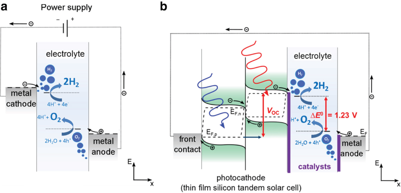
(a) Illustration of an electrolysis cell with power supply to split water into hydrogen and oxygen (b) Illustrated electrolysis cell where the power supply is replaced by an illuminated multi-junction (here: tandem) solar cell. Upon illumination electron-hole pairs are generated with a maximum energy as described by the split-up of the quasi-Fermi levels (EF,p&n). The maximum energy of an electron would be e⋅VOC. As indicated in b), electrodes will be usually covered with catalyst materials to keep the overpotential losses as low as possible. However, in principle the electrolysis could also work without catalyst at the cost of high overpotentials.
When illuminating such a device, electron-hole pairs are generated by photon absorption. The resulting charge carrier density is described in terms of the quasi Fermi levels EF,p and EF,n. The maximum output potential of these electronic charge carriers is given by the energy separation of the quasi Fermi levels. This is equivalent to the maximum achievable open circuit voltage VOC. In the case of multi-junction solar cells, this value is the sum of the individual quasi Fermi level splittings. EF,p and EF,n as indicated in Figure 1b. As the maximum power operation point of a solar cell is always below VOC one must increase the 1.6 V minimum potential by typically >0.1 V i.e. resulting in >1.7 V. If a single photoabsorber material had to provide such an output voltage of 1.7 V, the minimum bandgap energy for high quality photoabsorber materials would have to be typically between 0.4 eV and 0.6 eV higher than this [55]. When using an average value of 0.5 eV, this results in a band gap energy of 2.2 eV.
Figure 2 illustrates these considerations schematically. Starting with the thermodynamic energy for the water splitting process of 1.23 eV (bottom), overpotential and resistive losses yield a minimum energy in real systems of about 1.6 eV. To provide this energy with a solar cell, we add another 100 mV for the difference between VOC and operation point and end up with a required optical band gap of 2.2 eV, if a single photoabsorber [56] were to be used for watersplitting in a coupled stand-alone PV-EC device.
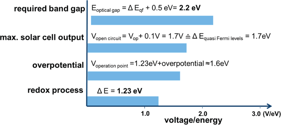
Potentials and energies relevant for water splitting using semiconductor based photo absorber materials. To have sufficient energies for water splitting in electrolysis a single photoabsorber would need a minimum bandgap of 2.2 eV. For details see text.
In fact, this is far from being the optimum energy gap for high efficiency solar light absorption and conversion. This can be easily understood by looking at the solar irradiation spectrum. Figure 3a [58] shows the solar spectrum vs. wavelength with some corresponding energies indicated. With a 2.2 eV band gap, one will only absorb a small portion of the solar spectrum, which results in a moderate maximum theoretical solar conversion efficiency of about 18% (Figure 3b). Furthermore, Figure 3b only depicts the optimum solar-to-electricity efficiency not considering any additional losses of the total system.
![Fig. 3: (a) Solar spectral irradiance vs. wavelength in space and at sea level. Also indicated are the corresponding photon energies on the top axis [plotted using empirical data from Reference Solar Spectral Irradiance: Air Mass 1.5, https://www.nrel.gov/grid/solar-resource/spectra-am1.5.html, accessed June 2019]. (b) Maximum solar light to electricity conversion efficiency for single junction solar cells as a function of the optical band gap “Shockley-Queisser-Limit” (adapted from Ref. [57]).](/document/doi/10.1515/zpch-2019-1453/asset/graphic/j_zpch-2019-1453_fig_003.jpg)
(a) Solar spectral irradiance vs. wavelength in space and at sea level. Also indicated are the corresponding photon energies on the top axis [plotted using empirical data from Reference Solar Spectral Irradiance: Air Mass 1.5, https://www.nrel.gov/grid/solar-resource/spectra-am1.5.html, accessed June 2019]. (b) Maximum solar light to electricity conversion efficiency for single junction solar cells as a function of the optical band gap “Shockley-Queisser-Limit” (adapted from Ref. [57]).
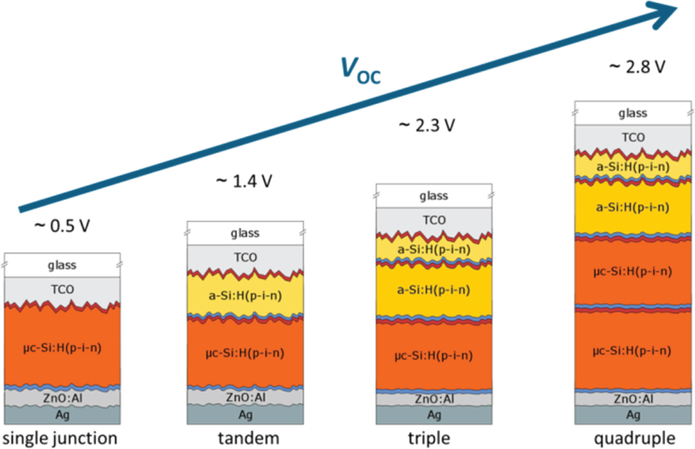
A straightforward way for getting an appropriately high output voltage while making sufficiently efficient absorption of the solar spectrum, is the use of multi-junction stacked solar cells – a well-established approach in solar cell manufacturing. Hereby individual solar cells are stacked on top of each other and connected in series such that the cell with the highest band gap is on top, absorbing the high energy part of the spectrum and letting the low energy part pass. The material with the lowest band gap is at the bottom absorbing light with energies that pass through the other cells on top. With such a series connection the output voltages of the individual cells add up while the total current is divided between the sub-cells [59]. Adequate candidates for such a cell stack are μc-Si:H and a-Si:H, which cover a range of optical gaps appropriate for efficient solar light absorption [60]. Figure 4 shows the optical absorption curves of a-Si:H and μc-Si:H. The data for c-Si is shown for comparison. As can be seen from the absorption curves, the combination of a-Si:H/μc-Si:H makes a very good match when used as a stack in solar cells with the a-Si:H having a high absorption coefficient in the blue part of the solar spectrum and the μc-Si:H absorbing a much larger portion of the red part of the solar spectrum. What makes these materials additionally attractive is the fact that they can be prepared with the same deposition processes (such as plasma enhanced chemical vapour deposition) by simple adjustment of the process parameters and that they can be alloyed with e.g. Ge, C, N, O to further tune the band gap and other material properties. Using these absorber material and going from single (μc-Si:H, a-Si:H) to tandem, triple, quadruple junctions, the open circuit voltage increases from 0.5 to almost 3.5 V while the short circuit current density decreases accordingly (Figure 5a) [35], [46], [61], [62]. All cells have similar overall efficiencies, which is also seen by the simulation curve with assumed 10% and 14% efficiency and fill factor (FF) of 72%. At the same time such a solar cell stack makes efficient use of the solar spectrum. This is demonstrated in Figure 5b which shows the quantum efficiency (QE) of a quadruple cell stack with the QE of the individual cells as solid lines and the sum of all four cells as shaded red area. Such a cell stack has typically an efficient absorption between 300 and 1100 nm, and provides voltages up to VOC = 2.8 V. Maximum solar cell efficiencies achieved during the present study were between 11.0 and 11.3% for a-Si:H/a-Si:H and a-Si:H/μc-Si:H tandem cells, 13.6% for a-Si:H/ a-Si:H/μc-Si:H triple junctions and 13.2% for a quadruple junction [46].
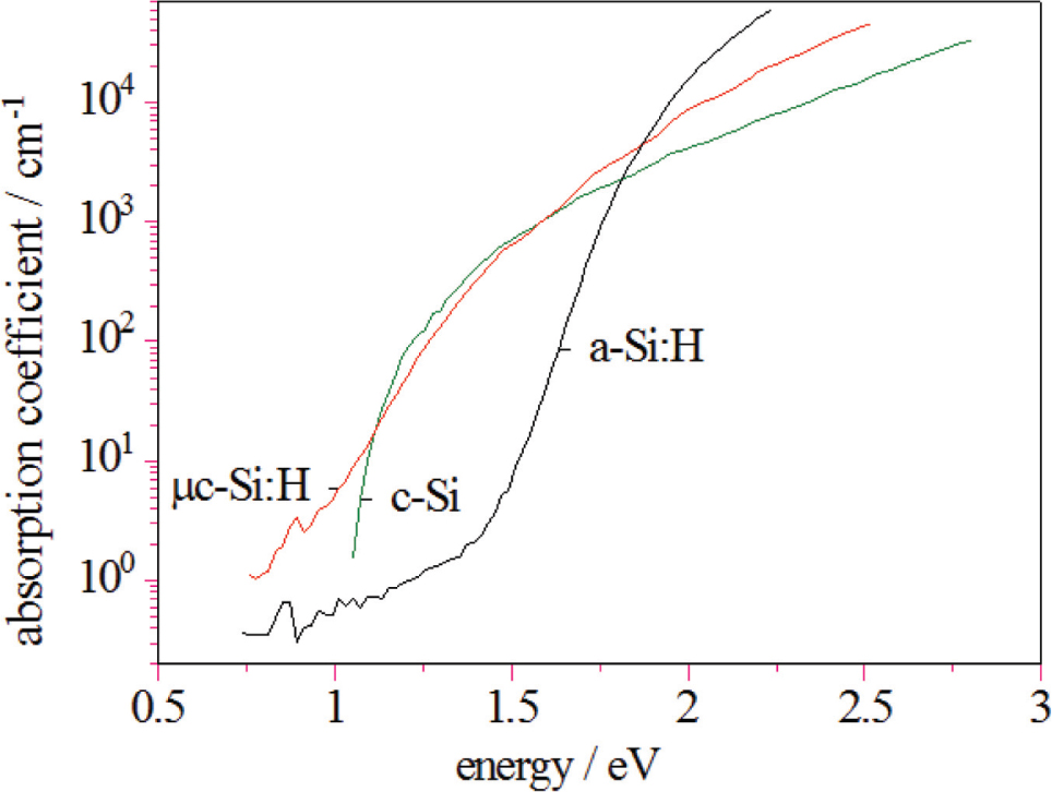
Optical absorption of a-Si:H, μc-Si:H and c-Si vs. photon energy.
![Fig. 5: (a) Short circuit current densities vs. open circuit voltage of single and multi-junction solar cells based on a-Si:H and μc-Si:H. As the number of sub-cells increases, the individual open circuit voltages add up while the total current has to be shared between the sub-cells. In the ideal case the overall efficiency would remain constant. This is also seen in the result of a simple simulation (dashed grey lines). The curves with corresponding JSC and VOC values are calculated from the formula ηPV = JSC x VOC x FF, for solar cell efficiencies ηPV equals 10% and 14%, respectively and a fill factor FF = 72% as typical value for thin film silicon based solar cells [46]. (b) Quantum efficiency vs. wavelength of a quadruple solar cell with the QE of the individual sub-cells (solid lines) and the sum of all cells (shaded area).](/document/doi/10.1515/zpch-2019-1453/asset/graphic/j_zpch-2019-1453_fig_005.jpg)
(a) Short circuit current densities vs. open circuit voltage of single and multi-junction solar cells based on a-Si:H and μc-Si:H. As the number of sub-cells increases, the individual open circuit voltages add up while the total current has to be shared between the sub-cells. In the ideal case the overall efficiency would remain constant. This is also seen in the result of a simple simulation (dashed grey lines). The curves with corresponding JSC and VOC values are calculated from the formula ηPV = JSC x VOC x FF, for solar cell efficiencies ηPV equals 10% and 14%, respectively and a fill factor FF = 72% as typical value for thin film silicon based solar cells [46]. (b) Quantum efficiency vs. wavelength of a quadruple solar cell with the QE of the individual sub-cells (solid lines) and the sum of all cells (shaded area).
Note: This approach is not the only possible solution. Alternatively one can use a close to ideal solar absorber such as c-Si with a band gap of 1.1 eV and make a lateral series connection which will give multiples of about 0.7 eV [26], [27]. We will briefly discuss this approach later.
With this in mind it is obvious that any single photoelectrode material to be used as power source in electrolysis processes will have to face these boundary conditions. Output voltages of about 1.7 V can only be delivered with a considerable loss in efficiency when sunlight illumination is to be used [56]. In contrast, for the semiconductor absorber materials in multi-junction solar cells such high optical band gaps are not needed because the output voltage is delivered as the sum of several cells [46], [59].
Consequently we have focused our development of the photovoltaic power generator for the coupled PV-EC device on the development of stacked multi-junction solar cells with amorphous and microcrystalline silicon based absorber materials.
We prepare thin film silicon solar cells in p-i-n configuration that is sandwiching an intrinsic absorber layer between p- and n-doped layers, which provide an internal field for charge carrier separation via drift. Cells are conventionally deposited on transparent conductive oxide (TCO) covered glass substrates and have an optically highly reflective ZnO/Ag back contact. The cells are illuminated through the glass/TCO substrate. For multi-junctions, sequences of p-i-n are stacked on top of each other with higher band gaps towards the glass/light entrance side. Typically we cover a range of VOC = 0.5–2.8 V from μc-Si:H single junction to a-Si:H/a-Si:H/μc-Si:H/μc-Si:H quadruple junctions [35], [62]. A schematic of the layer sequence of this range of solar cells is shown in Figure 6 [46].
Schematic of the structure of single and multi-junction solar cells with the TCO covered glass substrate, sequences of p-i-n layers (for each sub-cell the thick intrinsic absorber layer is embedded between the thin doped p (red)- and n(blue)-layers) and the ZnO:Al/Ag optically highly reflective back contact. Also indicated are the achievable open circuit voltages VOC.
2 Sample preparation and experiments
2.1 Solar cell fabrication
Solar cells were deposited on TCO-covered glass with substrate size 10 × 10 cm2. Two types of TCO were used: a commercially available fluorine doped tin-oxide (SnO2:F; ASAHI Type VU), and an etched aluminum doped zinc oxide (ZnO:Al) prepared in-house by magnetron sputtering. Both TCOs have a rough surface (indicated in Figure 6) with feature sizes of a few hundred nm up to 1 μm to increase optical scattering and thus improve optical absorption in the i-layer.
Amorphous and microcrystalline silicon (a-Si:H, μc-Si:H) layers were prepared by plasma enhanced chemical vapor deposition (PECVD) in multi-chamber PECVD systems from process gases silane and hydrogen. Control over the amorphous to microcrystalline volume fractions of the layers was obtained by variation of the silane-to-hydrogen process gas mixture. The optical band gap in a-Si:H was controlled by variation of the deposition temperature in the range 100 °C–200 °C. For doped layers phosphine or trimethylboron was added for n- and p-doping, respectively. Alternatively doped mixed phase (amorphous/microcrystalline) silicon oxide (a/μc-SiOx) layers were prepared with additional carbon dioxide gas [46].
The solar cell ZnO/Ag back contacts were deposited by sputtering processes. Back contact areas were defined by shadow masks and/or laser ablation processes.
In cases where solar cells smaller than the 10 × 10 cm2 size substrates were to be used (typically 1 cm2), these were firstly isolated by laser processes and then mechanically cut from the substrates.
For solar cells with larger total area of up to 64 cm2 two concepts of contact grid lines were investigated using combinations of shadow mask metallization and laser ablation processes (see below). For more details and process parameters of the solar cell fabrication see ref [36].
2.2 Catalyst deposition
In the combined PV-EC device the solar cell back electrode in direct contact with the electrolyzer has a multi-functional task. It must (i) be highly optically reflective, (ii) have low electrical resistance, (iii) be catalytically active and (iv) be chemically stable. In one approach we investigated various metal layers (Ag, Al, Au, Cu, Ni; Pt, Ti) and metal layer stacks (Al/Ni, Ag/Pt) for this purpose as solar cell back reflector and HER catalyst. Metals were deposited via electron beam evaporation with typical thickness of a few hundred nm [49].
RuO2 coated titanium (Metakem GmbH) or IrOx (titanium substrate, Metakem GmbH) was used as OER electrode catalyst for experiments with these HER metal combinations.
As alternative to high performance noble metal based catalysts – in particular in view of upscaling to large area PV-EC systems – we also prepared NiFeOx and NiMo as OER and HER catalyst materials. These were prepared via electrodeposition on areas of up to 50.3 cm2. Ni sheets with a thickness 300 μm were used as substrates [37].
2.3 Solar cell measurements
The current density – voltage (j-V) dependency of solar cells and of the combined PV-EC systems were measured under simulated AM1.5G illumination conditions at 25 °C. To study the performance for outdoor conditions, j-V measurements were also performed at temperatures up to 80 °C and the illumination was varied both with respect to intensity and spectral shape [50], [51], [52], [63].
For the development of multi-junction solar cells, measurement of quantum efficiencies of the individual cell components were performed [35].
2.4 Electrochemical measurements and PV-EC system design
Electrochemical performance of the various catalyst systems was measured both individually in two or three electrode configuration as well as in the combined PV-EC system under illumination. In most cases 0.1 M or 1.0 M KOH solution was used as electrolyte for measurements on the electrochemical part of the PV-EC system. In some selected applications we also used acidic electrolyte solutions (for example in ref. [36]).
As a PV-EC measurement system we started with a commercial cell (PECC-2) from Zahner-elektrik GmbH & Co KG. This device has the possibility to connect a solar cell but did not allow for exchange of the Pt counter electrode, which when used as OER electrode gave high overpotentials, and had no option to place a membrane or to separate gases. (Figure 7a).
![Fig. 7: (a) Commercially available PV-EC device build by Zahner (PECC-2, ZAHNER-elektrik GmbH & Co. KG) with replaceable working electrode and reference electrode close to the working electrode. Gas collection and electrolyte flow are possible, but the counter electrode cannot be replaced and the gasses cannot be separated [adapted from Zahner-Elektrik web-page, (b) In-house build PV-EC device with replaceable working and counter electrode, reference electrode close to the working electrode and 30 mL electrolyte reservoir. No electrolyte flow and gas collection/separation possible [46].](/document/doi/10.1515/zpch-2019-1453/asset/graphic/j_zpch-2019-1453_fig_007.jpg)
(a) Commercially available PV-EC device build by Zahner (PECC-2, ZAHNER-elektrik GmbH & Co. KG) with replaceable working electrode and reference electrode close to the working electrode. Gas collection and electrolyte flow are possible, but the counter electrode cannot be replaced and the gasses cannot be separated [adapted from Zahner-Elektrik web-page, (b) In-house build PV-EC device with replaceable working and counter electrode, reference electrode close to the working electrode and 30 mL electrolyte reservoir. No electrolyte flow and gas collection/separation possible [46].
For more flexibility in particular for investigating different types of electrode materials we built a PV-EC device compatible with our solar cell design, where electrodes could be exchanged easily (Figure 7b). However, gas separation and collection, electrolyte flow, or installation of a membrane was not possible.
The next step was to develop a PV-EC device which included all necessary features: flexibility concerning exchange and integration of all individual components (solar cells, catalysts, and membranes), functionality during operation (gas separation, exchange and pumping of electrolyte fluid) and measurement modus (2- vs. 3-electrode measurements). This system is shown in some detail with more description in Figure 8.
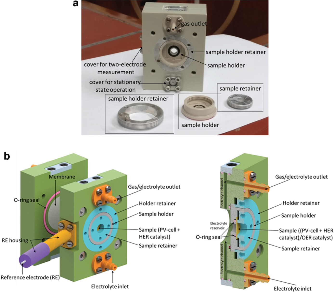
(a) Photograph of the PV-EC device in the two-electrode, stationary state configuration. The counter electrode side is shown with an empty counter electrode (sample) holder. The working electrode (sample) holder set is placed in front of the device. (b) PV-EC device made of polyether ether ketone (PEEK). The gas/electrolyte in- and outlets can be replaced by a cover, allowing electrolyte flow as well as stationary state operation. The reference electrode housing is shown in yellow and purple and can also be replaced by a cover for two- or three-electrode measurements. The two parts allow the implementation of a membrane in order to separate the half-cell reactions. The sample holder is shown in grey and cased by a metal sample holder retainer with screw threads (blue). In the cross section through the PV-EC device the electrode (sample) is shown in light yellow; the sample holder is shown in grey. The two metal retainers are depicted in blue. O-rings are used as sealing and shown in pink. Pumping through the electrolyte channels is possible.
For all above systems the maximum solar cell aperture area was 0.5 cm2.
Finally we focused on up-scaling a combined PV-EC system into a compact cassette. This is shown in Figure 9a and b. The system can carry a solar cell substrate of size 100 cm2. It is modular in the sense that one can easily replace solar cells, catalyst electrodes and membranes. It allows for gas separation and electrolyte flow. As it is designed in order to simulate real operation conditions, only 2-electrode operation is possible. As a special feature it contains a metal sheet (typically Ni foil with 300 μm–1 mm) which forms at the same time the substrate for HER and OER catalyst deposition as well as the electrical contact to the solar cell on the cathode (HER) side. Further solar cells to be used in this up-scaled system require a grid contact design to collect the current on the solar cell front contact. Details will be shown in the results section. The total active area of the solar cell in this set-up is 64 cm2. This corresponds to an area increase by a factor 128 as compared with the smaller PV-EC systems described above.
![Fig. 9: (a) Schematic cross section of the up-scaled coupled PV-EC device. The device is modularly built in the sense that each component can be exchanged easily and quickly (e.g. solar cell, catalysts, and membranes). The in- and outlets enable stationary state and flow measurements as well as gas collection and quantification. The contact design allows the measurement of the electronic properties of the individual parts (1+2: PV, 2+3: EC, 1+3: PV-EC). (adapted from [36]), (b) Photographs of the upscaled PV-EC device, showing the front side with the 10 × 10 cm2 substrate holded by a metal frame leaving an aperture for the 64 cm2 size interconnected solar cell, side view and back view with the back electrode serving as substrate for the OER catalyst.](/document/doi/10.1515/zpch-2019-1453/asset/graphic/j_zpch-2019-1453_fig_009.jpg)
(a) Schematic cross section of the up-scaled coupled PV-EC device. The device is modularly built in the sense that each component can be exchanged easily and quickly (e.g. solar cell, catalysts, and membranes). The in- and outlets enable stationary state and flow measurements as well as gas collection and quantification. The contact design allows the measurement of the electronic properties of the individual parts (1+2: PV, 2+3: EC, 1+3: PV-EC). (adapted from [36]), (b) Photographs of the upscaled PV-EC device, showing the front side with the 10 × 10 cm2 substrate holded by a metal frame leaving an aperture for the 64 cm2 size interconnected solar cell, side view and back view with the back electrode serving as substrate for the OER catalyst.
Further details of the measurement routines and additional experimental studies are provided in the following references: [36], [37], [46], [49].
3 Results
3.1 Amorphous and microcrystalline silicon for solar cells with high open circuit voltages
A main requirement for solar cells in our PV-EC device is a sufficiently high output voltage. It is therefore of interest to focus the material and solar cell optimization primarily on high open circuit voltage while not sacrificing total efficiency and with this current density (jSC) and fill factor (FF).
Figures 10 and 11 show results of our developments for a-Si:H and μc-Si:H. When a-Si:H is prepared at different substrate temperature this leads to a variation of the hydrogen concentration which in turn results in a variation of the optical band gap and consequently in the open circuit voltage achievable in solar cells. At the same time however, any deviation from the ideal substrate temperature which is in the range 200–250 °C, might cause deterioration of the electronic quality of the material. Therefore temperature variations have to be counterbalanced by adjustment of other deposition parameters such as hydrogen dilution, gas flow and pressure or discharge power. Figure 10 shows how the VOC can be varied between 800 and 946 mV when the substrate temperature is decreased from 250 °C to 110 °C. For the lower substrate temperatures (¡110 °C) a stronger hydrogen dilution, i.e. lower silane concentration SC is clearly beneficial. Total efficiencies remain in a range of about 8–10% showing that reasonable quality solar cells with a considerable range of output voltages for appropriate adjustment in multi-junction devices may be deposited [48], [64].
![Fig. 10: Photovoltaic parameters of single junction solar cells (efficiency ηPV (a), open-circuit voltage VOC (b), fill factor FF (c), and short-circuit current density JSC (d)) as a function of the substrate temperature Ts of the intrinsic a-Si:H layer, with 10% (blue squares) and 4% (red triangles) silane concentration SC, respectively. The intrinsic a-Si:H layers had a thickness of approx. 400 nm. The lines are to guide the eye. The data is taken from Refs. [48], [64].](/document/doi/10.1515/zpch-2019-1453/asset/graphic/j_zpch-2019-1453_fig_010.jpg)
Photovoltaic parameters of single junction solar cells (efficiency ηPV (a), open-circuit voltage VOC (b), fill factor FF (c), and short-circuit current density JSC (d)) as a function of the substrate temperature Ts of the intrinsic a-Si:H layer, with 10% (blue squares) and 4% (red triangles) silane concentration SC, respectively. The intrinsic a-Si:H layers had a thickness of approx. 400 nm. The lines are to guide the eye. The data is taken from Refs. [48], [64].
![Fig. 11: Solar cell parameters: (a) conversion effciencyηPV, (b) short-circuit current density JSC, and (c) fill factor FF vs. the open-circuit voltage VOC in a 1300 nm (black filled squares), a 650 nm (blue filled trianlges), and a 450 nm thick μc-Si:H absorber layer series (red filled stars), in a 1300 nm thickness combined with the SC profiling and incorporated buffer layer (50 nm) series (black open squares), in a 650 nm thickness combined with incorporated buffer layer (20 nm) series (magenta open triangles), and in a 450 nm thickness combined with incorporated buffer layer (5 nm) series (green open stars). The trends of the six series around the best-cell VOC are indicated by solid lines as a guide to the eye [47].](/document/doi/10.1515/zpch-2019-1453/asset/graphic/j_zpch-2019-1453_fig_011.jpg)
Solar cell parameters: (a) conversion effciencyηPV, (b) short-circuit current density JSC, and (c) fill factor FF vs. the open-circuit voltage VOC in a 1300 nm (black filled squares), a 650 nm (blue filled trianlges), and a 450 nm thick μc-Si:H absorber layer series (red filled stars), in a 1300 nm thickness combined with the SC profiling and incorporated buffer layer (50 nm) series (black open squares), in a 650 nm thickness combined with incorporated buffer layer (20 nm) series (magenta open triangles), and in a 450 nm thickness combined with incorporated buffer layer (5 nm) series (green open stars). The trends of the six series around the best-cell VOC are indicated by solid lines as a guide to the eye [47].
μc-Si:H is a phase mixture of amorphous and crystalline regions. It has an effective optical bandgap, and the open circuit voltage in solar cells may be varied as a function of the crystalline volume content. In addition the VOC depends on the μc-Si:H absorber layer thickness in solar cells and can further be influenced by a-Si:H based buffer layers between the doped and the intrinsic absorber layers in the p-i-n cell structure. Figure 11a–c shows results of optimization of solar cells with μc-Si:H absorber layer plotted as a function of the open circuit voltage. It is seen that for the individual parameter series in general current density, fill factor and efficiency decrease strongly for increased VOC. The lines in Figure 11 are only guides to the eye. The different behaviors of FF, JSC and η vs. VOC for the individual series is linked to the complex relationships between the structure composition of μc-Si:H, its homogeneity along the growth axis as an absorber layer in a solar cell and related with this, the interface to the p- and n- doped layers including the quality of nucleation and number of defects. These various contributions overlap and result in the observed complex dependencies. The overall general trend however for this material is that with increasing amorphous volume fraction the open circuit voltage increases but the optical absorption and with this the short circuit current decrease at a stronger rate resulting in lower efficiencies.
The optimization task was to keep these parameters high for higher VOC. This was achieved by careful adjustment of absorber layer thickness, process gas profiling during the absorber layer growth and application of buffer layers [46], [47], [48]. Solar cells with VOC of 570–580 mV with about 8% efficiency at current densities of 20 mA/cm2 were obtained.
With these materials and solar cells at hand multi-junction solar cells were prepared. One challenge in preparing stacked solar cells is that the current in the sub-cells should be evenly distributed such that no individual sub-cell with a low current will limit the total stack performance. Figure 12 shows an example of such a current matching process. In a three junction a-Si:H/a-Si:H/μc-Si:H an μc-SiOx:H layer [65] is introduced between the middle and the bottom cell as an intermediate optical reflector to enhance the current density in the middle cell (Figure 12). The QE curves of the two devices with and without intermediate reflector are also shown in Figure 12. We find that indeed the current density of the middle cell is enhanced, therefore reducing its limiting character and resulting in an overall efficiency enhancement from 13.1% to 13.6%. Similar adjustment, by introduction of intermediate reflectors or variation of the absorber layer thicknesses were performed for all multi-junction solar cells to achieve optimum current matching conditions, maintaining voltages and overall efficiency on a high level [35], [46].
![Fig. 12: Schematic of a triple junction solar cell showing the layer sequence with the position of the intermediate reflector and quantum efficiency QE for the triple junction cell with (red) and without (black) intermediate reflector. Also shown the current densities of the sub-cells calculated from the QE results [46].](/document/doi/10.1515/zpch-2019-1453/asset/graphic/j_zpch-2019-1453_fig_012.jpg)
Schematic of a triple junction solar cell showing the layer sequence with the position of the intermediate reflector and quantum efficiency QE for the triple junction cell with (red) and without (black) intermediate reflector. Also shown the current densities of the sub-cells calculated from the QE results [46].
3.2 Application of multijunction solar cells in combined PV-EC devices and solar-to-hydrogen efficiencies
A summary of the various types of multi-junction solar cells is given in the form of j-V curves for a-Si:H/a-Si:H and a-Si:H/μc-Si:H tandem, a-Si:H/a-Si:H/μc-Si:H and a-Si:H/μc-Si:H/μc-Si:H triple and a-Si:H/a-Si:H/μc-Si:H/μc-Si:H quadruple junctions in Figure 13 [46]. The VOC increases from 1.5 V to 2.8 V from the a-Si:H/μc-Si:H tandem to the quadruple cell with the jSC decreasing from 10 mA/cm2 to about 7 mA/cm2. Also indicated is the potential at 1.23 V which is the minimum for water electrolysis. We see that at that voltage level all types of cells would deliver sufficient voltage and current. However, when including the overpotential losses which are to be expected, this operation point will be shifted towards higher voltages, by at least 300–400 mV (compare Figure 2). In that case some of the solar cells may not have sufficient output voltage and the operation points may shift into the steep slope of the j-V curve.
![Fig. 13: Summary of current density voltage curves of typical tandem, triple and quadruple junction solar cells developed in the present work under AM1.5 light illumination. Cell size = 1 cm2. The dashed vertical line indicates the theoretical operation point of a PV-EC device at 1.23 V (without overpotential losses). In real PV-EC devices this operation point is shifted due to overpotential losses, which are plotted on the upper abscissa. From the respective photocurrent density at a certain overpotential one can estimate a maximum theoretical STH efficiency (right ordinate). For details see text, adapted from ref. [35].](/document/doi/10.1515/zpch-2019-1453/asset/graphic/j_zpch-2019-1453_fig_013.jpg)
Summary of current density voltage curves of typical tandem, triple and quadruple junction solar cells developed in the present work under AM1.5 light illumination. Cell size = 1 cm2. The dashed vertical line indicates the theoretical operation point of a PV-EC device at 1.23 V (without overpotential losses). In real PV-EC devices this operation point is shifted due to overpotential losses, which are plotted on the upper abscissa. From the respective photocurrent density at a certain overpotential one can estimate a maximum theoretical STH efficiency (right ordinate). For details see text, adapted from ref. [35].
These effects are seen nicely when the various multi-junction solar cells are connected with the electrolyzer in a combined PV-EC system (Figure 14) [46]. The current density of the entire device is plotted vs. the applied voltage. At zero bias (0 V) the device is driven without external bias i.e. only by the charge carriers generated by the solar cell under illumination. With the charge carrier energy being high enough, H2 and O2 are formed at the electrolyzer electrodes, the electric loop is closed and an electrical current can flow through the system. Comparing the j-V curves of the solar cell alone (Figure 13) with the PV-EC system (Figure 14) we observe two main effects: (i) the slope of the curve towards higher voltage gets less steep and (ii) the operation point (0 V) in the PV-EC device is shifted to the right. The first effect is mainly due to the additional and non-negligible resistance of the electrolyte (see also below). The second effect is a result of the catalyst overpotentials. In the case of the a-Si:H/μc-Si:H tandem cell, which as a solar cell alone provided the highest j-value, both effects lead to a considerable reduction of the maximum current densities obtainable at the operation point to almost zero mA/cm2.
![Fig. 14: Linear sweep voltammetry measurements of the PV-EC devices using silicon multi-junction solar cells (same as in Figure 13) with a Pt (HER) / RuO2(OER) catalyst pair in 0.1 M KOH at a scan rate of 30 mV/s. Aperture area for the solar cells was 0.5 cm2 in the measurement set-up shown in Figure 7b. The right ordinate depicts the achievable STH efficiency calculated from the photocurrent density at 0 V (see text), adapted from ref. [35].](/document/doi/10.1515/zpch-2019-1453/asset/graphic/j_zpch-2019-1453_fig_014.jpg)
Linear sweep voltammetry measurements of the PV-EC devices using silicon multi-junction solar cells (same as in Figure 13) with a Pt (HER) / RuO2(OER) catalyst pair in 0.1 M KOH at a scan rate of 30 mV/s. Aperture area for the solar cells was 0.5 cm2 in the measurement set-up shown in Figure 7b. The right ordinate depicts the achievable STH efficiency calculated from the photocurrent density at 0 V (see text), adapted from ref. [35].
From the current density at the operation point jOP we can make a simple calculation of a solar-to-hydrogen efficiency ηSTH using the following equation:
with the potential for the water splitting process of 1.23 V, the power density of the light illumination Pin (100 mW/cm2 in standard AM1.5G test condition) and the Faraday efficiency ηF, describing the percentage of charge carriers supplied from the illuminated solar cell which transform into hydrogen atoms. This value was determined to be close to 100% for our systems [35], [36]. The corresponding ηSTH values are shown on the right ordinates of Figures 13 and 14. Note that the STH value on the right hand y-axis in Figures 13 and 14 is only defined at the operation point jOP(V = 0) and that in Figure 13, the ηSTH values correspond to a theoretical maximum value just considering the operation point of the solar cell and assuming zero additional losses in the electrolyzer system. In Figure 14 the ηSTH should represent a fairly realistic value once the ηF is known precisely. These considerations also tell us that provided a solar cell delivers a sufficient voltage at the operation point (1.23 V + overpotentials) then it is the current density at the operation point which will determine the achievable ηSTH.
Knowing or having measured the overpotentials of the electrode/catalyst materials (VHER and VOER) and the resistance of the electrolyte (Rel), one can calculate the PV-EC j-V curve (VPV-EC) based upon a measured solar cell j-V curve (VPV). This allows estimations of various combinations of system components in series connection. The corresponding equation is:
Figure 15 shows these individual j-V curves and the calculated total VPV-EC(j) curve of a PV-EC device, which is in close agreement with the measured curve (green and black-dashed curves). This simple equivalent circuit model is a very valuable tool for system optimization and estimation of the influence of various system components [66], [67], [68].
![Fig. 15: Current density-voltage characteristics of the main four circuit components of the PV-EC device: the solar cell (VPV(j), orange curve), the RuO2 anode (OER(−j), red curve) with the associated ηOER, the Ni cathode (HER(j), light blue curve), with the associated ηHER, and the resistance of the electrolyte (jR, dark blue line). The voltammogram of the PV-EC device (VPV-EC(j), green curve) was computed via Eq. 2. The measured curve of the corresponding PV-EC devices (dashed black curve) matches the simulation very well (adapted from [46]).](/document/doi/10.1515/zpch-2019-1453/asset/graphic/j_zpch-2019-1453_fig_015.jpg)
Current density-voltage characteristics of the main four circuit components of the PV-EC device: the solar cell (VPV(j), orange curve), the RuO2 anode (OER(−j), red curve) with the associated ηOER, the Ni cathode (HER(j), light blue curve), with the associated ηHER, and the resistance of the electrolyte (jR, dark blue line). The voltammogram of the PV-EC device (VPV-EC(j), green curve) was computed via Eq. 2. The measured curve of the corresponding PV-EC devices (dashed black curve) matches the simulation very well (adapted from [46]).
Returning to the j-V curves of the various multi-junction solar cells in the combined PV-EC device with the Pt/RuO2 catalyst pair (Figure 14), the best performance was obtained for the aSi/aSi/μcSi triple junction. From the slope of the j-V curve, and considering the above discussion based upon the equivalent series connection model, one can infer that performance is also limited by the resistance of the electrolyte. This was confirmed by increasing the electrolyte concentration from 0.1 M to 1.0 M and thereby reducing its electrical resistance. This is shown in Figure 16. With the increased electrolyte concentration the shape of the j-V curve and the current density at the operation point (0 V) improve resulting in a solar-to-hydrogen efficiency of ηSTH = 9.5% (Pt/RuO2 catalyst pair; 0.5 cm2 aperture area solar cell) [35], [46].
![Fig. 16: Influence of the electrolyte concentration on the PV-EC device performance in a system with Pt/RuO2, catalyst pair at T = 25 °C, 1 sun (AM1.5G illumination). With increase of the electrolyte solution from 0.1 to 1.0 M, the respective resistance is reduced and the current density at the operation point (0 V) increases resulting in a maximum ηSTH = 9.5% for a 0.5 cm2 aperture area solar cell (adapted from ref [35]).](/document/doi/10.1515/zpch-2019-1453/asset/graphic/j_zpch-2019-1453_fig_016.jpg)
Influence of the electrolyte concentration on the PV-EC device performance in a system with Pt/RuO2, catalyst pair at T = 25 °C, 1 sun (AM1.5G illumination). With increase of the electrolyte solution from 0.1 to 1.0 M, the respective resistance is reduced and the current density at the operation point (0 V) increases resulting in a maximum ηSTH = 9.5% for a 0.5 cm2 aperture area solar cell (adapted from ref [35]).
Obviously a low series resistance inside the electrolyzer is highly beneficial. This can be achieved by reducing the cathode-anode electrode distance, with serious impact on controlling gas extractions and electrolyte flow, or by increasing the electrolyte concentration. The latter unfortunately will put additional constraint on the system stability as higher ionic concentrations may lead to corrosion damage of the metal or semiconductor materials. This can very clearly be seen in Figure 17 where long-term measurements of PV-EC systems in 0.1 and 1.0 M KOH solutions are compared. While in 0.1 M solution the systems remains stable beyond 10,000 seconds, in 1.0 M the systems fail at much shorter times of a few hundred seconds as indicated by the decrease in absolute numbers of the current density [35], [46].
![Fig. 17: Influence of the electrolyte concentration on the PV-EC device stability for a triple junction solar cell with Pt HER catalyst and a quadruple junction solar cell with a Ni HER catalyst. In both cases the systems fail much earlier in the higher concentration [35].](/document/doi/10.1515/zpch-2019-1453/asset/graphic/j_zpch-2019-1453_fig_017.jpg)
Influence of the electrolyte concentration on the PV-EC device stability for a triple junction solar cell with Pt HER catalyst and a quadruple junction solar cell with a Ni HER catalyst. In both cases the systems fail much earlier in the higher concentration [35].
3.3 The solar cell – electrolyzer contact
This brings us to the aforementioned critical solar cell/electrolyzer contact with its requirements of multi-functionality:
high optical reflectivity
low electrical contact resistance
high catalytic activity
high chemical and mechanical stability in view of aggressive electrolytes and outdoor operation with thermal cycle stress
Figures 18 and 19 show the performance of a number of metals with respect to their optical reflection as back contact in the solar cell (Figure 18) and the catalytic activity for the HER reaction as a cathode contact (Figure 19). For the optical back reflector the metals were deposited by electron beam evaporation directly on the n-doped Si layer of an a-Si:H/a-Si:H tandem solar cell without ZnO:Al interlayer. There are clear differences in the performances. The quality as optical back reflector is seen in the value of the short circuit current density with 7.7 mA/cm for the Ag layer and 6.4 mA/cm2 for the Ni layer (Figure 18). On the other hand the onset potential for HER is clearly lowest (best) for Pt and Ni while the layers with high optical performance show much higher onset potentials with low catalytic activity (Figure 19). Not surprisingly single metal contacts at the junction between the solar cell and the electrolyzer will likely not fulfill all requirements for high ηSTH performance. This leads to the application of metal stacks to separately provide good optical properties for the solar cell and high catalytic activity in the electrolyzer. In general such metal stacks should be straightforward to prepare. Figure 20 shows an example where we combined Al/Ni (as a low cost alternative) and Ag/Pt (as best performance material). We see that with the combination we obtain fairly good performance. The metals maintain their optical (Ag, Al) and catalytic (Pt, Ni) behavior also in the metal stack. Further we note that the low cost Al/Ni alternative has an onset potential similar to the noble metal Ag/Pt combination while still showing a reasonably high current density [46], [49].
![Fig. 18: Current density-voltage j−V measurements of a-Si:H/a-Si:H tandem solar cells with different metals as optical back reflector (note: without ZnO:Al interlayer), adapted from ref. [46].](/document/doi/10.1515/zpch-2019-1453/asset/graphic/j_zpch-2019-1453_fig_018.jpg)
Current density-voltage j−V measurements of a-Si:H/a-Si:H tandem solar cells with different metals as optical back reflector (note: without ZnO:Al interlayer), adapted from ref. [46].
![Fig. 19: Linear sweep voltammetry measurements, conducted in 0.1 M KOH, of single metal layers (approx. 150 nm of Al, Au, Ag, Cu, Ti, Ni, Pt; same as in Figure 18) on glass substrates at a scan rate of 10 mV/s, adapted from ref. [46].](/document/doi/10.1515/zpch-2019-1453/asset/graphic/j_zpch-2019-1453_fig_019.jpg)
![Fig. 20: Linear sweep voltammetry measurements in 0.1 M KOH at a scan rate of 30 mV/s under AM 1.5 illumination of the PV-EC devices with different single and double metal contacts, adapted from ref. [46].](/document/doi/10.1515/zpch-2019-1453/asset/graphic/j_zpch-2019-1453_fig_020.jpg)
Linear sweep voltammetry measurements in 0.1 M KOH at a scan rate of 30 mV/s under AM 1.5 illumination of the PV-EC devices with different single and double metal contacts, adapted from ref. [46].
3.4 Upscaling of a combined PV-EC device and development of non-noble metal based catalysts
What remains as a serious issue under long term operation of such combined PV-EC systems is the stability against chemical corrosion combined with mechanical instability. This will be of particular concern in any case where thin (deposited) metallic layers are used for the solar cell back contact and the catalyst electrode of the electrolyzer. Possible pin-holes introduced during deposition or created as a result of internal layer stress, which could be further enhanced by thermal cycling, will open up chemical reaction paths to the semiconductor or the very sensitive TCO layer in the solar cells. This will lead to corrosion, creation of electrical shunts and finally break-down of the PV-EC device.
Efforts have been made to overcome this by introducing chemically inert protection layers [23], [25], [69], [70] such as TiO2 and other corrosion resistant materials. In our work we have decided on a more simple but robust solution by introducing a metal sheet between the solar cell and the electrolyzer (compare Figure 9). Such a metal sheet, e.g. Ni with a thickness of a few hundred μm, will very effectively protect the solar cell from corrosion. It allows keeping the optimized ZnO/Ag back reflector, provides sufficient electrical contact, and serves as a substrate for the catalyst deposition with considerable reduced constraint on the catalyst deposition process which would otherwise have to be compatible with the entire solar cell as a substrate. The concept has been used for the small size substrate devices (see Figure 8) but in particular also for the up-scaled device (Figure 9). The Ni metal sheet is placed between the PV and the EC cell and serves at the same time as a substrate for the catalyst deposition. Similar metal sheets are also used on the anode side as catalyst substrate [36], [37]. It can be discussed to what extent, when using a few hundred μm thick metal sheet, the device still qualifies as “integrated” or to what extent the metal sheet already represents a wire connection. In both cases our device is a closely packed, combined PV-EC system, and as long as it has a metal back contact between the solar cell (PC) and the electrolyzer (EC), the solar cell is a buried junction anyway. We would therefore consider the conceptual difference as irrelevant.
Besides the development of catalysts for the up-scaled device (which will be presented below), the structuring of the solar cell front contact can be considered as a main issue for large size integrated PV-EC systems. For typical current densities of 10 mA/cm2, one ends up at a total current of 100 A for a 1 m2 size solar cell. Such current levels are impossible to transport laterally through the few hundred nm thick front TCO layer of the superstrate type of solar cell without unacceptable resistive losses (compare Figures 1 and 6). The conductance of the front contact has to be enhanced by an additional highly conductive metal grid. But different from the well-established lateral series interconnection of thin film modules [39], where individual solar cell stripes are connected in series resulting in much higher voltages, in our device concept we would want to have individual cell areas all connected in parallel as the cell stack already delivers the necessary voltage.
For this we have investigated two different approaches [36] of which one was particularly successful. A schematic of the process sequence is shown in Figure 21. After deposition of the solar cell stack (i) an opening is cut with a laser down to the TCO front contact (ii). Then the metal back contact is deposited, making also a connection to the front contact (iii). This latter connection is then isolated from the back contact by a second laser ablation process, leaving a separate access to the front contact with a metal grid (iv). Finally, the front contact is isolated and a planar electrical connection is made to the EC device i.e. the Ni sheet (v and vi; see also Figure 9). We end up with a pattern of 64 solar cells of 1 cm2 size on a 100 cm2 size substrate (Figure 21) which are all connected in parallel and where the front contact has a metal grid. The success of this approach is demonstrated in Figure 22. Figure 22a shows a comparison of the j-V curve of a 1 cm2 size cell with a 64 cm2 size cell without metal grid. We observe a strong decrease in both FF and jSC for the large size cell. Compared with this, the 64 cm2 size “tile” structure with laser processed metal grid has a much better performance (Figure 22b). The figure shows the j-V curves of the individual cells (grey lines), the arithmetic average (red line) and the measured large size device (dashed blue). Compared to the cell without grid (Figure 22a), FF and jSC have improved considerably. However, additional area losses (of typically a few percent depending on the size of the grid lines) have to be considered and overall the efficiency may decrease further for a further increase in substrate size.
![Fig. 21: Schematic of the process step sequence for the metal interconnect of a 64 cm2 size solar cell (left) and front view of the resulting tile structure with 64 parallel connected solar cells [36].](/document/doi/10.1515/zpch-2019-1453/asset/graphic/j_zpch-2019-1453_fig_021.jpg)
Schematic of the process step sequence for the metal interconnect of a 64 cm2 size solar cell (left) and front view of the resulting tile structure with 64 parallel connected solar cells [36].
![Fig. 22: (a) Comparison of current density – voltage curves of a triple junction solar cell with sizes 1 × 1 cm2 and 8 × 8 cm2 using only the front TCO contact for current extraction. With the increase in size, the series resistance increases while fill factor and short circuit current density decrease. (b) Current density – voltage curves of 64 individual solar cells with size 1 cm2 (grey lines), the arithmetic mean value of these individual cells (red line) and the measured curve of the interconnected individual cells (dashed blue), adapted from ref. [36].](/document/doi/10.1515/zpch-2019-1453/asset/graphic/j_zpch-2019-1453_fig_022.jpg)
(a) Comparison of current density – voltage curves of a triple junction solar cell with sizes 1 × 1 cm2 and 8 × 8 cm2 using only the front TCO contact for current extraction. With the increase in size, the series resistance increases while fill factor and short circuit current density decrease. (b) Current density – voltage curves of 64 individual solar cells with size 1 cm2 (grey lines), the arithmetic mean value of these individual cells (red line) and the measured curve of the interconnected individual cells (dashed blue), adapted from ref. [36].
Nevertheless, such 10 × 10 cm2 size substrates with 64 cm2 size aperture area solar cell structures have been successfully prepared with stacked solar cells and were integrated into the combined PV-EC device (Figure 9). Figure 23 shows results for such a combined device comparing Pt/IrOx with Ni/Ni catalyst pair as a function of operation time. We observe a stable performance over one hour for both catalyst pairs with a ηSTH = 2.1% and ηSTH = 4.8% for the Ni/Ni and the Pt/IrOx combination, respectively, thus confirming also the concept of metal sheets as protection layers [36].
![Fig. 23: Bias-free performance under illumination of the PV-EC cassette system (Figure 9) vs. operation time with a triple junction solar cell and front grid interconnect (Figure 21) of 64 cm2, comparing two catalyst systems (Ni/KOH/Ni) and (Pt/H2SO4/IrOx), adapted from ref. [36].](/document/doi/10.1515/zpch-2019-1453/asset/graphic/j_zpch-2019-1453_fig_023.jpg)
As a next step, non-noble metal based catalysts were developed for application in this up-scaled device.
Promising alternatives to the precious metal catalysts already exist especially for use in alkaline electrolytes. Based on literature reports we chose NiFeOX for the OER side and NiMo for the HER side [13], [71]. Besides promising low overpotentials in the range of 0.34–0.47 V (OER) and between 0.07 and 0.30 V for the HER side [13], [71], the materials can be readily prepared via electrodeposition on areas of 50 cm2 considered for application in our modular cassette device.
NiFeOX for OER was electrodeposited on Ni sheet substrates at room temperature from a 0.1 M electrolyte solution consisting of Ni(NO3) ⋅ 6H2O (98% Alfa Aesar) and FeCl2 ⋅ 4H2O (Emsure) dissolved in DI water. The ratio of Ni to Fe was varied from 100:0 to 60:40 (mol:mol).
NiMo for HER was electrodeposited on Ni sheet substrates at room temperature in an electrolyte solution consisting of NiSO4 ⋅ 6H2O (1), Na2MoO4 ⋅ 2H2O (2) and Na3C6H5O7 ⋅ 2H2O (3) (quantities: 3.19 g (1), 1.92 g (2), 3.52 g (3) [72]) dissolved in NH4OH [13], [72]. Deposition parameters were based on reports in the literature. Further details are described in ref. [37].
Figure 24 shows the two catalysts as deposited on the circular 50 cm2 Ni sheet substrates. The results of linear sweep voltammetry measurements using NiFeOx and NiMo as OER and HER catalysts, respectively are shown in Figure 25. Also in Figure 25 the IrOx/Pt and Ni/Ni catalyst pairs are shown for comparison. We observe for the NiFeOx/NiMo catalyst an excellent performance very similar to the noble metal catalyst pair and a clear improvement over the pure Ni/Ni pair used in earlier studies [36].
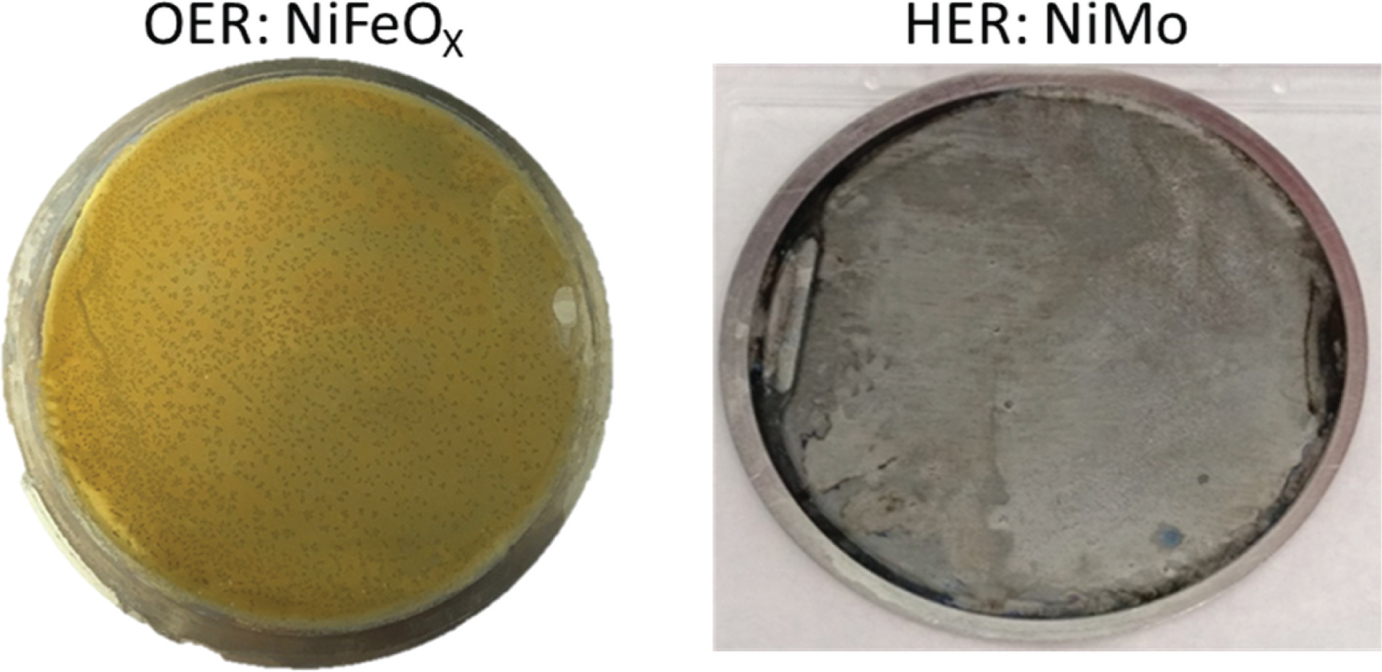
Photographs of the NiMo (HER) and NiFeOx (OER) catalysts deposited on 50.3 cm2 round Ni sheets for application in the PV-EC cassette system (Figure 9).
![Fig. 25: Current density-voltage curves of the catalyst systems Ni/Ni (blue triangles), IrOX/Pt (black squares) and NiFeOX/NiMo (red dots). The thermodynamic water splitting potential is indicated at 1.23 V (vertical guideline). The overpotentials are determined at 10 mA/cm2 (horizontal guideline), adapted from ref. [37].](/document/doi/10.1515/zpch-2019-1453/asset/graphic/j_zpch-2019-1453_fig_025.jpg)
Current density-voltage curves of the catalyst systems Ni/Ni (blue triangles), IrOX/Pt (black squares) and NiFeOX/NiMo (red dots). The thermodynamic water splitting potential is indicated at 1.23 V (vertical guideline). The overpotentials are determined at 10 mA/cm2 (horizontal guideline), adapted from ref. [37].
These NiFeOx/NiMo catalysts on Ni sheet substrates were then implemented into the PV-EC cassette (compare Figure 9 together with a triple junction solar cell with a laser patterned front contact (Figure 21). The resulting current-voltage curves under AM1.5 illumination are shown in Figure 26. Working in 1 M KOH electrolyte we conclude a solar-to-hydrogen efficiency ηSTH = 5.1% for the NiFeOx/NiMo catalyst pair in a cassette with a 64 cm2 size triple junction solar cell. With this value the non-noble metal based catalysts are more than a factor of two better than the earlier Ni/Ni pair results (Figure 23) and even slightly outperform the high quality noble-metal based catalysts IrOx/Pt [36], [37].
![Fig. 26: Current-voltage curves of a coupled PV-EC system in the cassette (Figure 9) under AM1.5 illumination in 1 M KOH with a triple junction solar cell (64 cm2) comparing the catalyst systems NiMo/NiFeOX and Pt/IrOX. The current at zero bias (V = 0 V, vertical guideline) is the operating current for unbiased, light induced water splitting. The different operating currents and resulting solar-to-hydrogen efficiencies are indicated (ηSTH(NiMo/NiFeOX) = 5.1 (±0.1)% and ηSTH(Pt/IrOX) = 4.8 (±0.1)%), adapted from ref. [37].](/document/doi/10.1515/zpch-2019-1453/asset/graphic/j_zpch-2019-1453_fig_026.jpg)
Current-voltage curves of a coupled PV-EC system in the cassette (Figure 9) under AM1.5 illumination in 1 M KOH with a triple junction solar cell (64 cm2) comparing the catalyst systems NiMo/NiFeOX and Pt/IrOX. The current at zero bias (V = 0 V, vertical guideline) is the operating current for unbiased, light induced water splitting. The different operating currents and resulting solar-to-hydrogen efficiencies are indicated (ηSTH(NiMo/NiFeOX) = 5.1 (±0.1)% and ηSTH(Pt/IrOX) = 4.8 (±0.1)%), adapted from ref. [37].
3.5 Simulated outdoor performance measurements with influence of temperature, spectral quality and stability under day-night cycle operation
In view of possible applications of PV-EC systems as stand-alone devices serious scientific and technical challenge are still to be met, let alone the economic aspects of this approach to store energy and/or generate chemical fuel from sun light.
It is therefore useful to address in advance some of these aspects in case such a system would be used let us say similar to a solar PV module on a house roof. We then would have e.g. variation in temperature, light intensity and spectral shape and not to forget day-night cycling for the solar cell and the electrochemical cell.
In Figure 27 results for the current-voltage curve behavior as a function of operating temperature for a triple junction solar cell (Figure 27a), Pt and RuO2 as HER and OER catalyst system (Figure 27b) and for the combined PV-EC system (Figure 27c) are shown [52]. For the solar cell alone, we observe the well-known behavior of reduction in open-circuit voltage and small increase in short-circuit current density as the temperature increases. Overall this leads to a decrease of the efficiency ηPV from about 13 to 12% with an increase of TOP from 25 °C to 60 °C. On the other hand we find that the catalytic behavior improves as concluded from the shift of the onset potential to lower values i.e. lower overpotentials. Consequently when combining the PV and the EC cell in a coupled device, the respective temperature characteristics could compensate each other. This is in fact confirmed by the data in Figure 27c, which shows the temperature behavior of a PV-EC coupled device. We observe in particular, that the current density at the operation point does not change as a function of temperature which means the solar-to-hydrogen efficiency ηSTH would remain at about 9.4% in the present case.
![Fig. 27: Operation temperature Top dependence of (a) current–voltage curves of an a-Si:H/a-Si:H/μc-Si:H triple junction solar cell (b) the cathodic and anodic current–voltage dependence of the Pt and RuO2 electrodes, respectively, in 1.0 M KOH and (c) the resulting current-voltage curves of the coupled PV-EC system [52].](/document/doi/10.1515/zpch-2019-1453/asset/graphic/j_zpch-2019-1453_fig_027.jpg)
Operation temperature Top dependence of (a) current–voltage curves of an a-Si:H/a-Si:H/μc-Si:H triple junction solar cell (b) the cathodic and anodic current–voltage dependence of the Pt and RuO2 electrodes, respectively, in 1.0 M KOH and (c) the resulting current-voltage curves of the coupled PV-EC system [52].
A change in temperature under outdoor conditions will also be introduced by changes in the illumination intensity. Frequently both effects occur simultaneously. In Figures 28 and 29 the combined effect of temperature and illumination intensity variation on a coupled PV-EC system is shown [50]. We observe that at all intensity levels investigated, the changes in PV cell behavior and onset potential of the catalyst system are qualitatively similar. The current at the operation point of the combined system normalized to the current at 25 °C (Figure 29) varies by less than ±2% for illumination intensities 1.0–0.364 suns and 25–60 °C. For the highest Tsyst = 80 °C investigated here the temperature effect on the solar cell behavior (see Figure 28) can no longer be compensated by the improved performance of the electrolyzer at all intensity levels. However for a wide range of illumination/temperature combinations, the combined PV-EC system is quite benign to these factors in terms of solar-to-hydrogen efficiency.
![Fig. 28: Combination of variation in system temperature and illumination intensity for the current-voltage curves of an a-Si:H/a-Si:H/μc-Si:H triple junction solar cell and the electrolysis cell with (Pt/IrOX) catalysts. The intersection point between PV cell and EC cell IV curve represent the operating current of the water splitting device at the respective intensity and temperature [50].](/document/doi/10.1515/zpch-2019-1453/asset/graphic/j_zpch-2019-1453_fig_028.jpg)
Combination of variation in system temperature and illumination intensity for the current-voltage curves of an a-Si:H/a-Si:H/μc-Si:H triple junction solar cell and the electrolysis cell with (Pt/IrOX) catalysts. The intersection point between PV cell and EC cell IV curve represent the operating current of the water splitting device at the respective intensity and temperature [50].
![Fig. 29: Normalized operation point current vs. system temperature Tsyst [50].](/document/doi/10.1515/zpch-2019-1453/asset/graphic/j_zpch-2019-1453_fig_029.jpg)
Normalized operation point current vs. system temperature Tsyst [50].
What also needs to be considered, in particular when stacked multi-junction solar cells are to be used, are changes in the spectral shape of the illumination light which will occur as a function of day time and season and which will in addition depend on geographical location. The overall efficiency of a stacked solar cell with different optical gaps depends critically on ideal current matching between the sub-cells. This current matching will usually be affected by variations in the illumination spectrum [73]. We have investigated such effect in terms of the average photon energy of the illumination spectrum (APE).
Figure 30 illustrates how the AM1.5 spectrum is modified with an additional blue LED to receive a change in the APE value. In Figure 31 the relative solar-to-hydrogen efficiencies over a ΔAPE range of 60 meV are seen to vary by ±5% for a combined PV-EC system with a triple junction and Pt/IrOx catalysts [50].
![Fig. 30: Blue modified spectrum (blue dashed curve) with an increased average photon energy of 1.75 eV compared to the AM1.5G spectrum (black solid curve) with an APE of 1.71 eV. The incident power of both spectra is 1000 W/m2. Operating temperature and incident illumination angle were constant at 25 °C and 0°, respectively [50].](/document/doi/10.1515/zpch-2019-1453/asset/graphic/j_zpch-2019-1453_fig_030.jpg)
Blue modified spectrum (blue dashed curve) with an increased average photon energy of 1.75 eV compared to the AM1.5G spectrum (black solid curve) with an APE of 1.71 eV. The incident power of both spectra is 1000 W/m2. Operating temperature and incident illumination angle were constant at 25 °C and 0°, respectively [50].
![Fig. 31: Solar-to-hydrogen efficiency plotted versus the average photon energy of the incident spectrum for a PV-EC device based on an a-Si:H/a-Si:H/μc-Si triple junction solar cell and the Pt/IrOX catalyst system. The colors illustrate, which LED was used to modify the spectrum and to achieve the respective APE [50].](/document/doi/10.1515/zpch-2019-1453/asset/graphic/j_zpch-2019-1453_fig_031.jpg)
Solar-to-hydrogen efficiency plotted versus the average photon energy of the incident spectrum for a PV-EC device based on an a-Si:H/a-Si:H/μc-Si triple junction solar cell and the Pt/IrOX catalyst system. The colors illustrate, which LED was used to modify the spectrum and to achieve the respective APE [50].
With this data available and published data on the annual irradiance (kWh/year ∗ m2) as a function of APE [74] one can estimate the yearly hydrogen production of a coupled PV-EC system with an aSi/aSi/μcSi triple junction (ηPV = 11.5%) and Pt/IrOx catalyst system as around 30,000 liter/(year∗m2) [63].
Finally a point of concern for any technical application of combined PV-EC systems will be the long-term stability under operation. Let us consider three aspects here:
chemical stability of the PV cell in contact with the electrolyte
chemical stability of the catalysts and the electrolyzer system
light induced degradation in a-Si:H based solar cells.
For (i) the chemical stability of the PV cell we think that a simple and straightforward solution is the introduction of a metal sheet between the solar cell back contact and the catalyst as presented. The concept allows us to work on system components independently and to exchange and investigate them in our coupled PV-EC systems.
For (iii) the light induced degradation (LID) of a-Si:H based solar cells it is known that the effects are less severe when stacked solar cells are used where the total intrinsic layer thickness is shared between the sub-cells. Furthermore the LID is found to be very little or even absent in solar cells with μc-Si:H absorber layers when introduced in a cell stack. The excellent stability against LID of multi-junction solar cells used in our PV-EC systems has been investigated and confirmed in ref [61], [75].
For the chemical stability of the catalysts (ii) we have investigated the non-noble metal based systems NiMo/NiFeOx in simulated day-night cycle operation. For this the catalyst pair has been operated in a two-electrode configuration at a current density of 10 mA/cm2 in 1 M KOH for 6 h, then kept (at zero current) in the dark for 18 h. This cycle has been repeated for 4 days. Results are shown in Figure 32. We observe a very stable and reproducible behavior for the NiMo/NiFeOx catalyst pair. For comparison the result for the Ni/Ni system is also shown where a considerably higher potential is needed to maintain the 10 mA/cm2 and where the system shows a degradation of the potential with time [37].
![Fig. 32: Electrolysis cell with a catalyst system consisting of NiMo/NiFeOX coated nickel sheet electrodes. Measurement of the system potential vs. time over 6 h for four consecutive days at −10 mA/cm2, intersected by 18 h resting time (no bias and no current flow). The performance of the Ni/Ni system is shown for comparison, adapted from ref. [37].](/document/doi/10.1515/zpch-2019-1453/asset/graphic/j_zpch-2019-1453_fig_032.jpg)
Electrolysis cell with a catalyst system consisting of NiMo/NiFeOX coated nickel sheet electrodes. Measurement of the system potential vs. time over 6 h for four consecutive days at −10 mA/cm2, intersected by 18 h resting time (no bias and no current flow). The performance of the Ni/Ni system is shown for comparison, adapted from ref. [37].
4 Discussion and conclusions
We have developed and investigated materials, devices and components for integrated PV-EC systems for hydrogen production via water splitting.
As the solar cell (PV) system we chose the a-Si:H and μc-Si:H based vertically stacked multi-junction solar cells. The absorber materials allow for a variation of optical gap in total by at least 100 mV. This together with a great flexibility in stacking individual cells on top of each other results in a wide and fine-tunable range of output voltages – ideally fitting with many electrochemical processes – and very good absorption matching with the solar spectrum. PV efficiencies are in the range of ηPV = 13–14%. For the resulting solar-to-hydrogen efficiencies it is crucial whether the catalyst/electrolyzer system with its overpotential will require a 2- or 3-junction device. For a three junction device with voltages of 1.8 V and beyond it is unlikely that current densities much higher than 9 mA/cm2 can be achieved resulting in theoretical maximum ηSTH of 11% assuming all other losses in the PV-EC system to be negligible. If catalysts with total overpotentials lower than 200 mV were to be found, then a tandem aSi/μcSi cell could be used with short circuit current densities exceeding 10 mA/cm2 and ηSTH = 12%.
The aSi/μcSi multijunction solar cell approach allows for a very compact total PV-EC system design, but will be limited in efficiency as discussed above to values not exceeding ηSTH = 12%. Apparently higher ηSTH values can be achieved using Si wafer solar cells [26], [27]. As an example we have evaluated a combination of a three-fold series connected Si heterojunction solar cell (SHJ) together with our best catalyst pairs (Figure 33). The SHJ are placed and connected like shingles (compare Figure 33) thereby reducing area losses. With an area of 58.5 cm2 this shingled module fits into the cassette system shown in Figure 9. From a combination of the corresponding j-V curves in the ideal case of no series resistance losses due to the cell connection we find the operation point at 11 mA/cm2 from which one can estimate ηSTH = 13.5%. This value gets close to published literature data of ηSTH = 14.2–14.5% [26], [27] using Si based solar cells in coupled PV-EC systems. It should be noted that c-Si series connected systems may sacrifice considerable efficiency potential in case individual cells are simply connected in series. With open circuit voltages of 700 mV (or 750 mV for highest efficiency cells), very likely only a combination of three cells will supply sufficient output voltage. Maximum current densities in this case will not exceed greatly 13 mA/cm2 resulting in a theoretical maximum ηSTH = 16%.
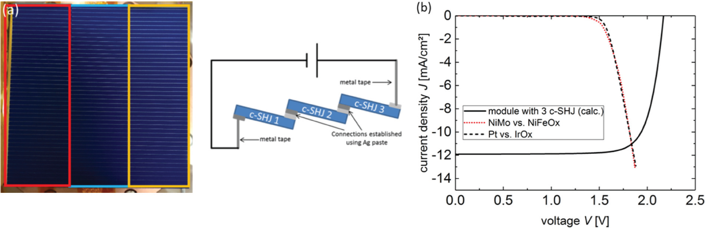
(a) Photograph and schematic of the module with three shingled crystalline silicon heterojunction solar cells. The different solar cells are indicated and were connected using silver paste. The active area is 58.5 cm2. (b) Current density-voltage curve of a module with three crystalline silicon heterojunction solar cells (produced at IEK-5 Photovoltaics), in the ideal case without series resistance losses due to the cell connection, plotted together with the curves of two catalyst systems in alkaline media.
Comparing the solar cell (PV) – electrolyzer (EC) coupled systems with approaches using photoelectrodes as absorber material it has to be pointed out, that multi-junction solar cells provide an excellent use of the solar spectrum resulting in high efficiencies ηPV as a basis for high ηSTH efficiencies. This can be achieved with a vertical stack of solar cells with different band gaps or alternatively with side-by-side connected solar cells with high ηPV such as crystalline silicon. Any single band gap photoabsorber which will have to deliver a sufficient output voltage on the other hand will necessarily have a much inferior ηSTH.
For the development of different area size cassette systems and especially for the upscaling to larger areas we have opted for a solution with a metal sheet between the solar cell and the electrolyzer (Figure 9). The metal sheet serves as a substrate for catalyst deposition and guarantees protection of the solar cell from corrosion by the electrolyte solution while still connecting the PV and the EC part functionally and electrically. We are aware that other solutions with deposited protection layers with possible advantages (weight, flexibility) are being worked on. However in the present study the use of protection layers was not further investigated.
A serious challenge for upscaling the PV part of the system is the application of an appropriate contact geometry to collect all current from the transparent solar cell front contact. Current values of 100 A are to be expected for 1 m2 size devices. Using a laser patterning technology we have developed a contact arrangement with parallel connected multi-junction solar cells (Figure 21). Such devices were used in up-scaled cassette systems showing reasonable performance for areas of 64 cm2 but also considerable room for further improvement. Similar interconnection will have to be developed for any large area PV system in a compact coupled PV-EC device. Concerning technical feasibility and efficiency corresponding solutions will then be in serious competition with optimized solar modules combined with an intelligent electronics for voltage adjustment and operation point tracking.
Based on literature reports we have prepared non-metal based HER and OER catalysts through electrodeposition on areas up to 50 cm2. The technology should be up-scalable to square-meter size substrates. The NiMo/NiFeOx catalyst pair shows excellent performance in alkaline (1 M KOH) solution where it even slightly outperforms the Pt/IrOx system. Further the catalysts show negligible degradation in simulated day-night cycles. With a total overpotential of 455 mV vs. 1.23 V at 10 mAcm2 (Figure 25) this sets a benchmark for an easy to deposit, abundant material based catalyst system of 50.3 cm2 size in alkaline media. As electrodeposition (electroplating) is a known process in industry for treatment of surfaces on meter-large scale and as the required chemicals for the NiMo/NiFeOx deposition are readily available, we would expect no technical problems for the further upscaling of the catalyst deposition on meter-size dimensions.
In view of possible outdoor application as stand-alone PV-EC coupled systems, realistic outdoor test conditions should also be investigated for estimation of hydrogen production volume and cost. This concerns variation in temperature, illumination intensity and spectral shape, and also long term operation in day-night cycles. For the multi-junction – multi band gap solar cells variation in the spectral shape will lead to current mismatching between the sub-cells and loss in efficiency. Adjustment of the cell design depending on the electrical operation point could be useful. As a benefit of the coupled PV-EC system it can be seen that the temperature characteristics of the PC and the EC part, respectively balance each other such that the solar-to-hydrogen efficiency remains unaffected over a certain temperature range. Also illumination intensity variation should be studied for the coupled systems as this may have effects different from corresponding variations on PV cells alone. Long-term operation studies for coupled systems, in particular for areas larger than typical laboratory size devices of 1 cm2, are to the best of our knowledge still missing.
For all PV-EC device developments we recommend using a simple equivalent circuit model which allows reliable predictions of system performance from measured or listed data of the individual components.
In conclusion a successful development of a PV-EC coupled system for hydrogen production from water splitting with aSi/μcSi type multi-junction solar cells was demonstrated on areas up to 64 cm2. Maximum efficiencies of 9.5% were demonstrated on 0.5 cm2 size and of 5.1% on 64 cm2. The investigations give a good basis for estimation of the maximum efficiency to be reached with the aSi/μcSi stack (12%) but also with alternative approaches with c-Si based solar cells (16%). Further improvement would be possible in case considerably enhanced catalyst pairs with total overpotential losses less than the herein shown 455 mV are developed and applied.
Acknowledgement
We are very grateful for the financial support within the DFG priority program SPP1613 “Fuels Produced Regeneratively Through Light-Driven Water Splitting: Clarification of the Elemental Processes Involved and Prospects for Implementation in Technological Concepts”. We thank all our colleagues from the Institute of Energy and Climate Research – Photovoltaic involved in this work and our colleagues from the project partner at the Technical University Darmstadt. In particular we would like to thank Jan-Philipp Becker, Stefan Haas, Niloofar Hamzelui, Sabine Kasper, Andreas Lambertz, Sandra Moll, Sascha Pust, Bugra Turan, Karen Wilken, Johannes Wolff, Christoph Zahren, and Uwe Rau (all IEK5-PV) and Thorsten Cottre, Joachim Klett, Florent Yang, Jürgen Ziegler, and Rolf Schäfer (all TUD) as well as Stephen Reynolds (University Dundee) for their important contributions and the fruitful collaboration. We further benefitted from collaboration and partial financial support within the project “Noble metal free catalysts for hydrogen production from renewable sources – Sustainable Hydrogen”, 03X3581B, funded by the Federal Ministry of Education and Research, where we want to thank in particular our collaboration partners at Evonik Industries AG Creavis Technologies & Innovation.
References
1. M. G. Walter, E. L. Warren, J. R. McKone, S. W. Boettcher, Q. Mi, E. A. Santori, N. S. Lewis, Chem. Rev. 110 (2010) 6446.10.1021/cr1002326Search in Google Scholar PubMed
2. J. W. Ager, M. R. Shaner, K. A. Walczak, I. D. Sharp, S. Ardo, Energy Environ. Sci. 8 (2015) 2811.10.1039/C5EE00457HSearch in Google Scholar
3. H.-J. Lewerenz, L. Peter, H. Frei, F. Schüth, T. S. Zhao, Photoelectrochemical Water Splitting – Materials, Processes and Architectures, The Royal Society of Chemistry, Cambridge, 2013.10.1039/9781849737739Search in Google Scholar
4. Y. Tachibana, L. Vayssieres, J. R. Durrant, Nat. Photonics 6 (2012) 511.10.1038/nphoton.2012.175Search in Google Scholar
5. S. Ardo, D. Fernandez Rivas, M. A. Modestino, V. Schulze Greiving, F. F. Abdi, E. Alarcon Llado, V. Artero, K. Ayers, C. Battaglia, J. P. Becker, D. Bederak, A. Berger, F. Buda, E. Chinello, B. Dam, V. Di Palma, T. Edvinsson, K. Fujii, H. Gardeniers, H. Geerlings, S. M. Hashemi, S. Haussener, F. Houle, J. Huskens, B. D. James, K. Konrad, A. Kudo, P. P. Kunturu, D. Lohse, B. Mei, E. L. Miller, G. F. Moore, J. Muller, K. L. Orchard, T. E. Rosser, F. H. Saadi, J. W. Schüttauf, B. Seger, S. W. Sheehan, W. A. Smith, J. Spurgeon, M. H. Tang, R. Van De Krol, P. C. K. Vesborg, P. Westerik, Energy Environ. Sci. 11 (2018) 2768.10.1039/C7EE03639FSearch in Google Scholar
6. Z. Chen, H. N. Dinh, E. Miller, Photoelectrochemical Water Splitting, Springer-Verlag, New York, 2013.10.1007/978-1-4614-8298-7Search in Google Scholar
7. K. Sivula, F. Le Formal, M. Grätzel, ChemSusChem 4 (2011) 432.10.1002/cssc.201000416Search in Google Scholar PubMed
8. T. Yao, X. An, H. Han, J. Q. Chen, C. Li, Adv. Energy Mater. 8 (2018) 1800210.10.1002/aenm.201800210Search in Google Scholar
9. K.-J. Lee, J.-W. Lee, J.-H. Lee, Y. Zhang, Y.-J. Heo, J. BajGai, S.-J. Park, Catalysts 8 (2018) 655.10.3390/catal8120655Search in Google Scholar
10. V. Smirnov, K. Welter, F. Finger, F. Urbain, J. R. Morante, B. Kaiser, W. Jaegermann, In: Photoelectrochem. Sol. Cells. N. D. Sankir, M. Sankir (Eds.). John Wiley & Sons And Scrivener Publishing LLC, Hoboken and Beverly (2018), P. 349–384.10.1002/9781119460008.ch9Search in Google Scholar
11. I. Holmes-Gentle, F. Alhersh, F. Bedoya-Lora, K. Hellgardt, In: Photoelectrochem. Sol. Cells. N. D. Sankir, M. Sankir, (Eds.). John Wiley & Sons And Scrivener Publishing LLC, Hoboken and Beverly (2018), P. 1–41.10.1002/9781119460008.ch1Search in Google Scholar
12. J. H. Kim, D. Hansora, P. Sharma, J. W. Jang, J. S. Lee, Chem. Soc. Rev. 48 (2019) 1908.10.1039/C8CS00699GSearch in Google Scholar
13. C. C. L. McCrory, S. Jung, I. M. Ferrer, S. Chatman, J. C. Peters, T. F. Jaramillo, J. Am. Chem. Soc. 137 (2015) 4347.10.1021/ja510442pSearch in Google Scholar PubMed
14. M. Gong, D. Wang, C. Chen, B. Hwang, H. Dai, Nano Res. 9 (2016) 28.10.1007/s12274-015-0965-xSearch in Google Scholar
15. S. Anantharaj, S. R. Ede, K. Sakthikumar, K. Karthick, S. Mishra, S. Kundu, ACS Catal. 6 (2016) 8069.10.1021/acscatal.6b02479Search in Google Scholar
16. I. Roger, M. A. Shipman, M. D. Symes, Nat. Rev. Chem. 1 (2017). DOI 10.1038/s41570-016-0003.10.1038/s41570-016-0003Search in Google Scholar
17. F. Urbain, P. Tang, V. Smirnov, K. Welter, T. Andreu, F. Finger, J. Arbiol, J. R. Morante, ChemSusChem 12 (2019) 1428.10.1002/cssc.201802845Search in Google Scholar PubMed
18. F. F. Abdi, L. Han, A. H. M. Smets, M. Zeman, B. Dam, R. Van De Krol, Nat. Commun. 4 (2013) 1.10.1038/ncomms3195Search in Google Scholar
19. H. Lu, V. Andrei, K. J. Jenkinson, A. Regoutz, N. Li, C. E. Creissen, A. E. H. Wheatley, H. Hao, E. Reisner, D. S. Wright, S. D. Pike, Adv. Mater. 30 (2018). DOI 10.1002/adma.201804033.10.1002/adma.201804033Search in Google Scholar PubMed
20. J. Brillet, J. H. Yum, M. Cornuz, T. Hisatomi, R. Solarska, J. Augustynski, M. Graetzel, K. Sivula, Nat. Photonics 6 (2012) 824.10.1038/nphoton.2012.265Search in Google Scholar
21. V. Andrei, R. L. Z. Hoye, M. Crespo-Quesada, M. Bajada, S. Ahmad, M. De Volder, R. Friend, E. Reisner, Adv. Energy Mater. 8 (2018) 1801403.10.1002/aenm.201801403Search in Google Scholar
22. S. Hu, M. R. Shaner, J. A. Beardslee, M. Lichterman, B. S. Brunschwig, N. S. Lewis, Science 344 (2014) 1005.10.1126/science.1251428Search in Google Scholar PubMed
23. B. Seger, T. Pedersen, A. Laursen, P. Vesborg, O. Hansen, I. Chorkendorff, J. Am. Chem. Soc. 135 (2013) 1057.10.1021/ja309523tSearch in Google Scholar PubMed
24. Y. W. Chen, J. D. Prange, S. Dühnen, Y. Park, M. Gunji, C. E. D. Chidsey, P. C. McIntyre, Nat. Mater. 10 (2011) 539.10.1038/nmat3047Search in Google Scholar PubMed
25. J. Ziegler, F. Yang, S. Wagner, B. Kaiser, W. Jaegermann, F. Urbain, J. P. Becker, V. Smirnov, F. Finger, Appl. Surf. Sci. 389 (2016) 73.10.1016/j.apsusc.2016.07.074Search in Google Scholar
26. J.-W. Schüttauf, M. A. Modestino, E. Chinello, D. Lambelet, A. Delfino, D. Dominé, A. Faes, M. Despeisse, J. Bailat, D. Psaltis, C. Moser, C. Ballif, J. Electrochem. Soc. 163 (2016) 1177.10.1149/2.0541610jesSearch in Google Scholar
27. S. Nordmann, B. Berghoff, A. Hessel, B. Zielinsk, J. John, S. Starschich, J. Knoch, Sol. Energy Mater. Sol. Cells 191 (2019) 422.10.1016/j.solmat.2018.11.004Search in Google Scholar
28. O. Khaselev, J. A. Turner, Science 280 (1998) 425.10.1126/science.280.5362.425Search in Google Scholar PubMed
29. A. Nakamura, Y. Ota, K. Koike, Y. Hidaka, K. Nishioka, M. Sugiyama, K. Fujii, Appl. Phys. Express 8 (2015) 107101.10.7567/APEX.8.107101Search in Google Scholar
30. W. H. Cheng, M. H. Richter, M. M. May, J. Ohlmann, D. Lackner, F. Dimroth, T. Hannappel, H. A. Atwater, H. J. Lewerenz, ACS Energy Lett. 3 (2018) 1795.10.1021/acsenergylett.8b00920Search in Google Scholar
31. S. Tembhurne, F. Nandjou, S. Haussener, Nat. Energy 4 (2019) 399.10.1038/s41560-019-0373-7Search in Google Scholar
32. J. Jia, L. C. Seitz, J. D. Benck, Y. Huo, Y. Chen, J. W. D. Ng, T. Bilir, J. S. Harris, T. F. Jaramillo, Nat. Commun. 7 (2016) 13237.10.1038/ncomms13237Search in Google Scholar PubMed PubMed Central
33. T. J. Jacobsson, V. Fjallstrom, M. Sahlberg, M. Edoff, T. Edvinsson, Energy Environ. Sci. 6 (2013) 3676.10.1039/c3ee42519cSearch in Google Scholar
34. A. C. Nielander, M. R. Shaner, K. M. Papadantonakis, S. A. Francis, N. S. Lewis, Energy Environ. Sci. 8 (2015) 16.10.1039/C4EE02251CSearch in Google Scholar
35. F. Urbain, V. Smirnov, J.-P. Becker, A. Lambertz, F. Yang, J. Ziegler, B. Kaiser, W. Jaegermann, U. Rau, F. Finger, Energy Environ. Sci. 9 (2016) 145.10.1039/C5EE02393ASearch in Google Scholar
36. J.-P. Becker, B. Turan, V. Smirnov, K. Welter, F. Urbain, J. Wolff, S. Haas, F. Finger, J. Mater. Chem. A 5 (2017) 4818.10.1039/C6TA10688ASearch in Google Scholar
37. K. Welter, N. Hamzelui, V. Smirnov, J.-P. Becker, W. Jaegermann, F. Finger, J. Mater. Chem. A 6 (2018) 15968.10.1039/C8TA05066JSearch in Google Scholar
38. K. Tolod, S. Hernández, N. Russo, Catalysts 7 (2017) 13.10.3390/catal7010013Search in Google Scholar
39. S. Haas, A. Gordijn, H. Stiebig, Prog. Photovoltaics Res. Appl. 16 (2008) 195.10.1002/pip.792Search in Google Scholar
40. J. J. Hanak, Sol. Energy 23 (1979) 145.10.1016/0038-092X(79)90115-4Search in Google Scholar
41. S. Klein, S. Wieder, S. Buschbaum, M. Rohde, K. Schwanitz, T. Stolley, C. Stömmer, D. Severin, A. Straub, U. I. Schmidt, K. Ahmed, Phys. Status Solidi C 8 (2011) 2978.10.1002/pssc.201001221Search in Google Scholar
42. K. Yamamoto, A. Nakajima, M. Yoshimi, T. Sawada, S. Fukuda, T. Suezaki, M. Ichikawa, Y. Koi, M. Goto, T. Meguro, T. Matsuda, M. Kondo, T. Sasaki, Y. Tawada, Sol. Energy 77 (2004) 939.10.1016/j.solener.2004.08.028Search in Google Scholar
43. J. Meier, U. Kroll, S. Benagli, L. Fesquet, J. Steinhauser, D. Borello, J. B. Orhan, Y. Djeridane, E. Vallat-Sauvain, M. Fecioru-Morariu, B. Mereu, J. Kalas, J. Hoetzel, P. Losio, M. Kupich, O. Kluth, T. Eisenhammer, D. Weidman, S. Marjanovic, G. Kohnke, Energy Procedia 15 (2012) 179.10.1016/j.egypro.2012.02.021Search in Google Scholar
44. A. Terakawa, Sol. Energy Mater. Sol. Cells 119 (2013) 204.10.1016/j.solmat.2013.06.044Search in Google Scholar
45. B. Yan, J. Yang, S. Guha, J. Vac. Sci. Technol. A Vacuum, Surfaces, Film. 30 (2012) 04D108.10.1116/1.4707154Search in Google Scholar
46. F. Urbain, Light induced water splitting using multijunction thin film silicon solar cells. In: Energy & Environment, Schriften des Forschungszentrum, Jülich, Vol. 323, (2016), ISBN 978-3-95806-148-4.Search in Google Scholar
47. F. Urbain, V. Smirnov, J.-P. Becker, U. Rau, F. Finger, J. Ziegler, B. Kaiser, W. Jaegermann, J. Mater. Res. 29 (2014) 2605.10.1557/jmr.2014.308Search in Google Scholar
48. F. Urbain, K. Wilken, V. Smirnov, O. Astakhov, A. Lambertz, J.-P. Becker, U. Rau, J. Ziegler, B. Kaiser, W. Jaegermann, F. Finger, Int. J. Photoenergy 2014 (2014) 249317.10.1155/2014/249317Search in Google Scholar
49. F. Urbain, V. Smirnov, J. P. Becker, U. Rau, J. Ziegler, F. Yang, B. Kaiser, W. Jaegermann, S. Hoch, M. Blug, F. Finger, Chem. Phys. Lett. 638 (2015) 25.10.1016/j.cplett.2015.08.018Search in Google Scholar
50. K. Welter, V. Smirnov, J.-P. Becker, P. Borowski, S. Hoch, A. Maljusch, W. Jaegermann, F. Finger, ChemElectroChem 4 (2017) 2099.10.1002/celc.201700112Search in Google Scholar
51. V. Smirnov, K. Welter, J. Becker, F. Urbain, W. Jaegermann, F. Finger, Energy Procedia 102 (2016) 36.10.1016/j.egypro.2016.11.315Search in Google Scholar
52. F. Urbain, J.-P. Becker, V. Smirnov, J. Ziegler, F. Yang, B. Kaiser, W. Jaegermann, S. Hoch, A. Maljusch, U. Rau, F. Finger, Mater. Sci. Semicond. Process. 42 (2016) 142.10.1016/j.mssp.2015.08.045Search in Google Scholar
53. M. F. Weber, M. J. Dignam, J. Electrochem. Soc. 131 (1984) 1258.10.1149/1.2115797Search in Google Scholar
54. I. Holmes-Gentle, K. Hellgardt, Sci. Rep. 8 (2018) 12807.10.1038/s41598-018-30959-9Search in Google Scholar PubMed PubMed Central
55. H. J. Snaith, J. Phys. Chem. Lett. 4 (2013) 3623.10.1021/jz4020162Search in Google Scholar
56. R. M. Navarro Yerga, M. C. Álvarez Galván, F. del Valle, J. A. Villoria de la Mano, J. L. G. Fierro, ChemSusChem 2 (2009) 471.10.1002/cssc.200900018Search in Google Scholar PubMed
57. T. Kirchartz, U. Rau, Adv. Energy Mater. 8 (2018). DOI 10.1002/aenm.201703385.10.1002/aenm.201703385Search in Google Scholar
58. The figure was created using empirical data from Reference Solar Spectral Irradiance: Air Mass 1.5, https://www.nrel.gov/grid/solar-resource/spectra-am1.5.html, accessed June 2019.Search in Google Scholar
59. A. De Vos, J. Phys. D. Appl. Phys. 13 (1980) 839.10.1088/0022-3727/13/5/018Search in Google Scholar
60. C. Ross, Y. Mai, R. Carius, F. Finger, Progess Photovoltaics Res. Appl. 17 (2011) 715.10.1002/pip.1093Search in Google Scholar
61. F. Urbain, V. Smirnov, J.-P. Becker, A. Lambertz, U. Rau, F. Finger, Sol. Energy Mater. Sol. Cells 145 (2015) 142.10.1016/j.solmat.2015.07.033Search in Google Scholar
62. V. Smirnov, F. Urbain, A. Lambertz, F. Finger, Energy Procedia 102 (2016) 64.10.1016/j.egypro.2016.11.319Search in Google Scholar
63. K. Welter, Solar Driven Water Electrolysis Based on Silicon Solar Cells and Earth-Abundant Catalysts (PhD Thesis), Technische Universität Darmstadt, 2019.Search in Google Scholar
64. K. Wilken, Tandem Cells Providing High Open Circuit Voltages for Photoelectrochemical Water Splitting (Master Thesis), Technische Universität Darmstadt, Germany, 2013.Search in Google Scholar
65. V. Smirnov, A. Lambertz, S. Moll, M. Bär, D. E. Starr, R. G. Wilks, M. Gorgoi, A. Heidt, M. Luysberg, B. Holländer, F. Finger, Phys. status solidi a 213 (2016) 1814.10.1002/pssa.201533022Search in Google Scholar
66. J.-P. Becker, F. Urbain, V. Smirnov, U. Rau, J. Ziegler, B. Kaiser, W. Jaegermann, F. Finger, Phys. Status Solidi A 213 (2016) 1738.10.1002/pssa.201533025Search in Google Scholar
67. F. Urbain, V. Smirnov, J. Becker, U. Rau, J. Ziegler, B. Kaiser, W. Jaegermann, F. Finger, Sol. Energy Mater. Sol. Cells 140 (2015) 275.10.1016/j.solmat.2015.04.013Search in Google Scholar
68. J. Ziegler, B. Kaiser, W. Jaegermann, F. Urbain, J. P. Becker, V. Smirnov, F. Finger, ChemPhysChem 15 (2014) 4026.10.1002/cphc.201402552Search in Google Scholar PubMed
69. D. Bae, S. Shayestehaminzadeh, E. B. Thorsteinsson, T. Pedersen, O. Hansen, B. Seger, P. C. K. Vesborg, S. Ólafsson, I. Chorkendorff, Sol. Energy Mater. Sol. Cells 144 (2016) 758.10.1016/j.solmat.2015.10.020Search in Google Scholar
70. J. Ziegler, Photoelektrosynthese von Wasserstoff Mit Silizium-Dünnschicht-Tandemsolarzellen (PhD Thesis), Technische Universität Darmstadt, urn:nbn:de:tuda-tuprints-46954, 2015.Search in Google Scholar
71. A. S. Batchellor, S. W. Boettcher, ACS Catal. 5 (2015) 6680.10.1021/acscatal.5b01551Search in Google Scholar
72. C. Fan, D. L. Piron, A. Sleb, P. Paradis, J. Electrochem. Soc. 141 (1994) 382.10.1149/1.2054736Search in Google Scholar
73. S. Reynolds, V. Smirnov, Energy Procedia 84 (2015) 251.10.1016/j.egypro.2015.12.321Search in Google Scholar
74. T. Minemoto, S. Fukushige, H. Takakura, Sol. Energy Mater. Sol. Cells 93 (2009) 1062.10.1016/j.solmat.2008.11.051Search in Google Scholar
75. F. Urbain, V. Smirnov, J. P. Becker, F. Finger, ACS Omega 1 (2016) 832.10.1021/acsomega.6b00259Search in Google Scholar PubMed PubMed Central
© 2020 Friedhelm Finger et al., published by De Gruyter, Berlin/Boston
This work is licensed under the Creative Commons Attribution 4.0 International License.
Articles in the same Issue
- Frontmatter
- Part III: Device Development
- Photoelectrochemical Water Splitting using Adapted Silicon Based Multi-Junction Solar Cell Structures: Development of Solar Cells and Catalysts, Upscaling of Combined Photovoltaic-Electrochemical Devices and Performance Stability
- Water Oxidation Catalysts from Waste Metal Resources: A Facile Metal-Organic Electrochemical Approach
- Various CO2-to-CO Electrolyzer Cell and Operation Mode Designs to avoid CO2-Crossover from Cathode to Anode
- Nanocrystalline Ga–Zn Oxynitride Materials: Minimized Defect Density for Improved Photocatalytic Activity?
- Integrated Devices for Photoelectrochemical Water Splitting Using Adapted Silicon Based Multi-Junction Solar Cells Protected by ALD TiO2 Coatings
- Stability and Degradation Mechanismof Si-based Photocathodes for Water Splitting with Ultrathin TiO2 Protection Layer
- Co3O4/BiVO4 Heterostructures for Photochemical Water Oxidation: The Role of Synthesis Parameters and Preparation Route for the Physico-Chemical Properties and the Catalytic Activity
- Cu2O/TiO2 Nanowire Assemblies as Photocathodes for Solar Hydrogen Evolution: Influence of Diameter, Length and NumberDensity of Wires
- Preface
- DFG priority program SPP 1613 “Fuels Produced Regeneratively Through Light-Driven Water Splitting”