Innovations in perovskite solar cells: a journey through 2D, 3D, and 2D/3D heterojunctions
-
Anum Sehar


Abstract
Perovskite solar cells (PSCs) have garnered significant attention in the photovoltaic community due to their exceptional performance, cost-effective manufacturing, and potential for diverse optoelectronic applications. Despite their promise, maintaining the operational stability of PSCs remains a critical challenge. In recent years, nanostructured materials, particularly two-dimensional (2D), three-dimensional (3D), and their 2D/3D heterojunction combinations, have emerged as innovative solutions to enhance PSCs’ stability and photovoltaic efficiency. This review examines recent advancements in PSCs utilizing these materials. It begins with an introduction to the fundamentals of perovskite-based photovoltaics and progresses to analyzing the role of 2D, 3D, and 2D/3D materials in optimizing PSC components. Key challenges in this field are also highlighted, alongside innovative strategies to overcome them, thus providing insights into the future direction of PSC technology.
1 Introduction
The growing global energy demand and associated environmental crises underscore the urgency of transitioning to sustainable energy solutions. 1 Solar energy, with its unmatched abundance and accessibility, has emerged as a leading candidate to address these challenges. 2 Among the various photovoltaic technologies, perovskite solar cells (PSCs) have garnered significant attention due to their remarkable efficiency, cost-effectiveness, and potential for large-scale implementation. 3 The advancements in PSCs have been transformative, with power conversion efficiencies (PCEs) surpassing 25.2 % for single-junction devices and reaching an unprecedented 32.5 % for tandem configurations in 2023. 4 These breakthroughs are attributed to innovative material engineering, particularly the development of two-dimensional (2D), three-dimensional (3D), and hybrid 2D/3D heterojunctions.
The success of PSCs lies in their unique material properties, including tunable band gaps, superior light absorption, and excellent charge transport characteristics. The integration of 2D materials such as MXenes, graphene, and TiS2 has been instrumental in addressing issues related to stability and efficiency. These materials improve charge carrier dynamics and reduce recombination losses, achieving efficiencies as high as 23.78 % in modified devices. Simultaneously, 3D materials contribute to enhanced structural integrity and mechanical resilience, with hybrid designs combining the advantages of both dimensionalities. For instance, devices incorporating 2D/3D heterojunctions have demonstrated PCEs exceeding 25 %, coupled with improved operational stability under humid and high-temperature conditions.
Because they promise to reduce pollution and generate renewable energy, several solar cells of numerous types have been developed. Experts have been paying close attention to thin-film solar cells like organic solar cells and perovskite solar cells due to their versatility, mobility, and adaptability. Power conversion efficiency (PCEs) peaked at 25.2 % for single-junction PSCs and 17.4 % for OSCs. 5
The Russian Mineralogist L. A. Perovski gave his namesake mineral, perovskite, the explicit valuable stone structure ABX3 (X = halogen, oxygen). The A cation shares a cubo octahedral site with twelve X anions, whereas the B cation acts as a counterion in an octahedral site with just six X anions. Due to their superconductivity or ferroelectricity, oxides are the most cautious perovskites. Less interest was paid to halide perovskites until it was shown that covered organometal halide perovskites transitioned from semiconductor to metal with increasing dimensions. 6
Weber first revealed the production and actual properties of PSCs in 1978; the organometal halide (X = Br, Cl, or I, M = Sn or Pb), which is CH3NH3MX3, is the main element for the PSCs, now receiving tremendous attention. 7 The size of the unit cell border in CH3NH3PbX3 rises from 5.68 Å to 5.92 Å–6.27 Å when the size of the halide increases from X = Cl to Br and I. Mixing halides may significantly alter the lattice parameters in the cubic stage; for example, CH3NH3PbBr2.07I0.93 displayed a = 6.03, CH3NH3PbBr0.45I2.55 showed a = 6.25, and CH3NH3PbBr2.3Cl0.7 displayed a = 5.98. CH3NH3SnBrxl3x (x = 0–3) crystallizes to the cubic perovskite assembly with a = 6.01 (x = 2), a = 6.24 (x = 0), and a = 5.89 (x = 3), In contrast to their lead-based counterparts, several tin-based perovskite compounds have shown electrical conductivity. 8
Large organic cations like C4H9NH3 and phenyl-ethyl ammonium often produce two-dimensional halide perovskite materials. 9 These heavy organic cations are placed into Pb–I octahedron repeat units to create 2D halide perovskites. The 2-dimensional halide perovskite materials are environmentally stable because Vander Waals interactions with the octahedral PbI6 units encapsulate the organic cations (PEA+ and BA+). In addition, the high exciton binding energies, poor charge transport, and wide bandgap of 2D halide perovskite PSCs contribute to their low power conversion efficiency. 10 The problems with two-dimensional halide perovskite have been addressed by combining it with the more traditional three-dimensional lead halide perovskite, a material in which the benefits of both types of perovskite are maximized. Creating a 3D/2D structure not only increases the performance of PSCs but also guarantees the structural integrity of the perovskite crystal phase and leads to long-term stability. 11 For instance, researchers developed a new method for making stable and effective PSCs via perovskite hybridization by constructing 2-dimensional or 3-dimensional perovskite hybrids to combine their merits. 12 Compared to pure 3D perovskite, two-dimensional or three-dimensional perovskite hybrids significantly improved device moisture stability in high humidity (65 %) without encapsulation. Notably, the 2D/3D perovskite hybrid film kept 54 % of its original efficiency after 220 h and exhibited no degradation after 40 days. Researchers successfully produced highly efficient and robust two-dimensional or three-dimensional hybrid perovskite solar cells employing 2-thiophene methylammonium as the spacer cation in 2019. 13
In this study, we detail the research and development that has led to the creation of perovskite solar cells that are both efficient and durable. Employing single-element two-dimensional materials (graphene, antimonene, bismuthine, phosphorene, and borophene), three-dimensional materials, and 2D/3D heterojunction materials for PSCs. Firstly, we will provide a concise introduction to PSCs. Next, the paper showcases the effective use of several elemental 2D, 3D, and 2D/3D materials in various layers of PSCs. The study finishes by emphasizing the significant accomplishments in this rapidly expanding field of research and addressing the issues that need to be addressed.
2 Perovskites solar cell
2.1 Constructional aspects of PSCs
To comprehensively assess solar cells within their broader context, it is essential to first understand their underlying mechanisms of energy generation. 14 , 15 Photovoltaic cells may be classified into two main configurations, namely inverted (p-i-n) and conventional (n-i-p), depending on the presence of carrier material (either electron or hole) on the outer side of the cell that comes into contact with incoming light first. 16 Furthermore, it is possible to categorize these two collections as mesoscopic or planar cells. In contrast to the exclusively planar architecture seen in mesoscopically fabricated perovskite devices, the planarly created perovskite devices include a mesoporous layer. Furthermore, it has been verified that perovskite devices are capable of operating in the absence of holes or electron transport layers. A considerable body of research has been dedicated to the examination of six specific categories of perovskite solar cells, including mesoscopic n-i-p configurations, planar n-i-p configurations, planar p-i-n configurations, mesoscopic p-i-n conformations, ETL-free structures, and HTL-free structures.
2.2 PSCs history
Perovskite is an inorganic-organic hybrid chemical that makes up the perovskite solar cell. 17 This material is an excellent charge carrier conductor and solar energy collector. The use of perovskite materials in solar cell manufacturing has undergone a dramatic upheaval since 2009. Power conversion efficiencies have improved dramatically and emerged as a hallmark of this revolution. Publications beginning in the early 1990s detail the advent of study into perovskite as a solar absorber.
In 2006, a team of Japanese researchers achieved a remarkable power conversion efficiency of 2.2 percent. This is a significant step forward, and its significance has been generally acknowledged. Dye-sensitized solar cells containing CH3NH3PbBr3 were employed in the experiment. 18 In 2009, CH3NH3PbBr3 was shown to be effective as a disinfectant, making it the first organic halide compound to be discovered. The power conversion efficiency of the CH3NH3PbBr3 device was found to be 3.81 %, whereas that of the CH3NH3PbI3 device was found to be 3.13 %. After further evaluation, the same team found that the CH3NH3PbI3 chemical, in combination with an iodine liquid electrolyte contact and enhanced production conditions, had a PCE value of 6.5 %.
However, the breakdown of perovskite nanocrystals inside the iodine liquid electrolyte was the cause of this PSC’s instability. Since then, many scientists have explored this field to improve the power conversion efficiency of perovskite solar cells. 19 Because of its fundamental photophysical qualities, functioning, and distinguishing traits, this technology has led to several advances in optoelectronic applications. 20 Many interesting electrical properties, such as piezoelectricity, thermoelectricity, superconductivity, and semiconductivity, are found in perovskite materials. The materials utilized determine these characteristics. In light of these positive features, notable experimental findings elucidating the underlying mechanism responsible for these substances’ enhanced power conversion efficiency, diverse techniques used in their production, and a substantial improvement in efficiency above 25 % have been documented within a limited timeframe. Solar state DSSCs were fabricated using the perovskite solar absorber CH3NH3PbI3 and the hole transport material Spiro-OMeTAD, yielding a power conversion efficiency of 9.7 percent. 21 The DSSC has shown significant gains in device stability compared to devices using liquid electrolytes. Researchers have made tremendous progress in solving the problem of device stability, but they still face a significant barrier to commercialization and large-scale production.
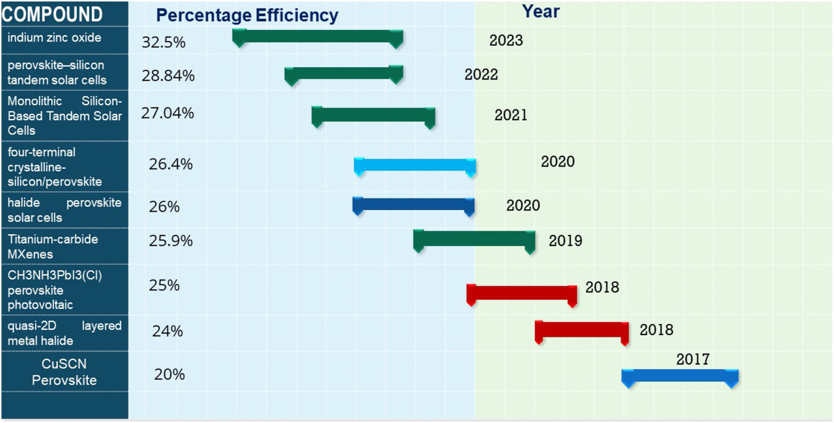
To address the problem of low power efficiency, researchers in 2023 used a very thin (5 nm) layer of amorphous indium zinc oxide as the interconnecting transparent conductive oxide. By using thin IZO rear electrodes and enhanced front contact stacks, together with optical improvements, a certified power conversion efficiency of 32.5 % was achieved. This PCE is one of the highest recorded for perovskite/silicon tandems. Ultrathin transparent contact method resulted in a significant reduction of around 80 % in indium usage. 22 The evolution of PSCs over the last few years with maximum power efficiency achieved is shown in Figure 1.
2.3 Addressing energy challenges with perovskite innovations
The global energy landscape faces a dual crisis: escalating energy demand and the adverse environmental impact of fossil fuel dependence. Renewable energy, particularly solar energy, stands out as a sustainable alternative due to its abundant availability and minimal carbon footprint. However, the efficiency, scalability, and affordability of current photovoltaic technologies remain barriers to their widespread adoption. Hybrid perovskite materials have emerged as a transformative solution in the photovoltaic field. Their unique properties, including high power conversion efficiency (PCE), tunable bandgaps, and low-cost fabrication, make them strong contenders for next-generation solar cells. Compared to silicon-based photovoltaics, perovskites enable lighter, flexible, and potentially cheaper devices with comparable or superior efficiencies. Additionally, their adaptability to various structural configurations – such as 2D, 3D, and hybrid 2D/3D – allows researchers to address challenges like long-term stability and environmental resistance. 29
Recent advances in 2D/3D perovskite hybrids represent a significant leap forward in addressing the stability-efficiency trade-off. These hybrid structures combine the superior stability of 2D perovskites with the high efficiency of 3D counterparts. For example, strategies such as defect passivation, enhanced energy-level alignment, and advanced crystallization techniques have resulted in record-breaking efficiencies and improved operational durability. 30
By mitigating challenges such as ion migration, environmental degradation, and charge recombination, hybrid designs are making perovskite solar cells increasingly viable for industrial application. 31 Exploring these advancements provides critical insights into scalable, energy-efficient, and sustainable solar technologies.
3 Large-scale PSC fabrication methods
The commercialization of PSCs depends on three factors: performance, cost, and reliability. Because of advancements in device design and manufacturing techniques, photovoltaic solar cells are now on an inexorable ascent (Figure 2). Perovskite solar cells may soon be commercialized due to the establishment of prototype production lines. With these production lines, perovskite photovoltaic devices with suitable performance characteristics may be mass-produced at a reasonable cost while still adhering to time-tested manufacturing practices. However, there are ongoing issues with device stability in the academic and commercial sectors.
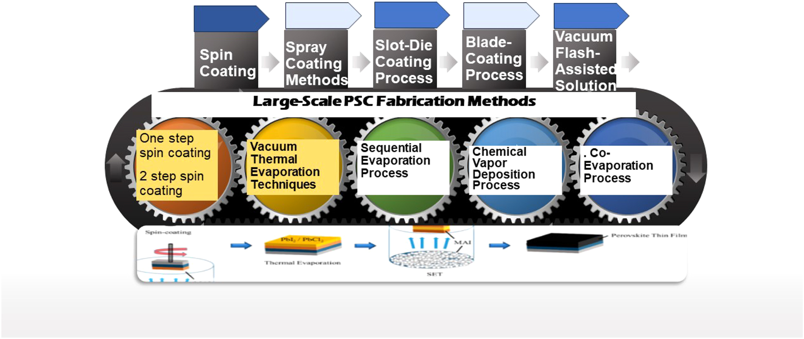
Various large-scale PSC fabrication methods.
Thin films of the spin-coating method have been the standard for producing metal-organic perovskite. That involves applying the material in a solution. This technology might allow for rapid iteration, enhancement, and the discovery of new information. However, this technique cannot accomplish bulk production of solar cells. To make a production process scalable, reducing manufacturing costs is crucial. This entails not only the initial investment in machinery but also the ongoing expenditures of operating the company, such as the cost of electricity, the price of materials, post-production waste treatment expenses, and the cost of quality assurance. 32 , 33 Because of their widespread availability, modern PSC materials are inexpensive. Therefore, investing in gear and equipment is the most expensive element of creating PSCs, although this cost may be lowered by increasing productivity and optimizing procedures. 34 Different substrate materials need different approaches to synthesis, making it necessary to categorize PSCs as either rigid or flexible. Perovskite thin films are typically manufactured by solution processing or vapor deposition techniques. 35
Our findings are based on the two clustering methods in other relevant studies.
The vacuum thermal evaporation process is no longer widely used in industry.
PSC researchers have also reduced blade coating and spray coating.
Ink-jet printing and slot-die coating have become prevalent at PSC research facilities.
Technical obstacles have slowed the commercialization and synthesis of large-area perovskites, but researchers are working to overcome these obstacles.
Some methods of perovskite thin-film production, such as thermal evaporation, have yet to be fully utilized to construct large-area solar cells despite their significant scaling potential.
Recent works have shown the higher power conversion efficiency for large-area PSCs with a slot-die coating, indicating that this coating may play a crucial role in the eventual commercialization of PSCs.
3.1 Spin coating
Spin coating is a batch process where a liquid layer is “pinned” onto a revolving substrate using centrifugal force. The method has been used to create several devices with a width of 1 cm and a surface area of 0.1 cm2. The steps of this method may be classified into two broad categories. The power conversion efficiencies of spin-coated perovskite devices have risen to 9.4 %. 36
The spin coating may make relatively large-area PSCs, as shown by the researchers, 35 , 37 who demonstrated a manufactured perovskite film area of 57 cm2 by carefully managing the solvent evaporation rate. Perovskite deposition is enhanced by a two-step sequential processing strategy instead of a single-step one. Film quality may also be improved by carefully managing post-annealed time and crystal formation. 38 , 39
3.1.1 One-step spin coating process
To experiment, lead halide salts and lead bromide are combined with organic halide salts (formamidinium iodide and methylammonium iodide in a solvent like dimethyl sulfoxide or N, N-dimethylformamide). The absorber and conductive layer (electrons or holes for transport) are doused with the combined precursor solution. Annealing is then conducted, which leads to the creation of perovskite films. 40 , 41
3.1.2 Two-step spin coating process
Isopropanol and dimethylformamide dissolve the halide organic compounds and lead halide salts. After the electron and hole transport layers have been annealed, the lead halide solution is spin-coated onto them. The MAI solution is spin-coated onto a lead halide surface, and then perovskite layers are formed by interdiffusion processes during annealing. Researchers subjected Perovskite solar cells with an area of 1 cm2 to a two-step spin coating procedure and then determined a PCE of 20.1 %. They effectively controlled the leftover PbI2 on the perovskite’s surface. 42
3.1.3 Advantages
Using this method, the chemistry and thickness of the perovskite layer may be manipulated with relative ease. 43 The study demonstrates the utilization of precursor solutions, including solvents with a high boiling point that are polar aprotic, i.e., DMF or DMSO. 44 , 45 This is because when a high rpm is used to spin the substrate, the solvents are often flushed out owing to centrifugal force.
3.1.4 Disadvantages
According to the research, 43 Perovskite films degrade in quality and homogeneity as the spin coating area grows. Controlling stoichiometry and crystallinity in a single phase of solution processing has proven difficult. These difficulties result from the precursor solution’s limited reactivity and the annealing procedure’s inability to complete the reaction fully. According to the results, spin coating is not an appropriate method for producing perovskite films on a big scale and over a wide region. 46 Lead is a necessary ingredient in the solution technique, just as in conventional procedures. However, it has been shown that over 50 % of spin-coating methods used to synthesize perovskite films are useless and must be thrown away. 47 , 48 Nonuniform perovskite films are formed using traditional antisolvents like chlorobenzene in large-area spin coating. 49
3.2 Spray coating methods
Because of its low ink concentration needs, compatibility with large-area technology, and low operating temperature, the spray coating process sees widespread usage in industrial settings. 50 Very scalable methods may be used to fabricate large-area thin perovskite films. The technique used to produce the perovskite layer yields a consistent material across large areas. The process begins with the creation of ink droplets and continues through their deposition into the substrate, their combination into a wet film, and finally, their drying. Spray coating is the most adaptable of the technologies that can be ramped up. The one-step technique and the two-step method are used for depositions now. Aprotic solvents are often used in one-step film deposition solutions. 50 , 51 Aprotic solvents, those without a hydroxyl group, amine groups, or acidic protons, are used in the second phase of a two-step procedure to apply metal salts by spin coating or spray coating. 35 , 52
Spray coating is a popular method for producing scalable substrates because of the speed by which capillary waves may be induced in a fluid. 43 The procedure entails breaking up a fluid into smaller droplets and depositing them onto a surface that can handle them. High-flow gas, ultrasonic stimulation, and ink cavitation are a few methods that may induce atomization. 53 , 54 Scalability is a common feature of atomization, as mentioned above methods.
Modern technical advancements in ultrasonic spray coaters have efficiently produced various functional thin films for solar cells. 54 Many different goals have motivated liquid thin-film coating technology research and development.
Organic salts may be deposited on a substrate using either a covering with a spray or soaking in alcohol. Isopropanol is used as a solvent in this process. 55 There is a noticeable variation in the outcomes depending on the method used to deposit the perovskite solutions. Many different mixtures of methylammonium iodide, lead iodide, and iodide chloride have been synthesized using a single-step deposition method. 56 , 57 The experiment used DMSO, GBL-DMSO, DMF-DMSO, DMF, and GBL as solvents. Hydrogen iodide and other processing additives were also used in some studies. For perovskite films made using this method, the highest power conversion efficiency was 18.1 percent for small-area specimens and 15.5 percent for the most extensive device area of 40 cm2. 58
No ultrasonic spray coater was used in the research, but they could determine the area of the device with the highest efficiency and most preferable form. 52 Perovskite was created by spraying a single-cation mixed halide over a preheated substrate, according to the study authors. Previous research 53 showed that this method yielded a favorable crystallization shape. Several scientific applications rely heavily on ultrasonic atomization, including temperature control, metal polyhalide complex, nucleation processes, solution optimization, and synthesis.
Since spray coating with nanoparticles is a simple manufacturing technology, it has been given much attention as a possible approach for advancing semi-transparent electronics. Researchers have used carbon nanotubes, silver nanowires, and spray-coated electrodes for transparency and their equivalent composites to produce tiny photovoltaic devices with a surface area of 0.25 cm2. Translucent in appearance, these devices were constructed completely using solution-based methods. Additionally, PCEs of greater than 10 % were obtained. 59 , 60 , 61
3.2.1 Advantages
There is potential for rapid, low-waste, and large-scale production of PSC devices. 50 Improved droplet size homogeneity, increased airflow, and more precise control over spray cone dispersion are only some of the hallmarks of modern ultrasonic spray coaters. 54 Uniform nucleation, faster supersaturation, reduced antisolvent consumption, faster antisolvent dispersion, and better homogeneity across a large surface area are some of the additional benefits of spray coating over conventional antisolvent dropping technique.
3.2.2 Disadvantages
Perovskite solar cells made using spray coating often have worse photovoltaic performance than PSCs made using blade or slot-die coating. As a result, refining the spray coating method for producing large-area perovskite films is crucial. 49
Single-step experiments frequently yield low-quality perovskite films, with architectures characterized by non-uniform crystallization, mostly dendritic structures, and insufficient coverage of the underlying transport layer. 35 This results in lower open-circuit voltages, short-circuit currents, and fill factors for photovoltaic cell devices compared to spin-coated devices. Low shunt resistance might be to blame for this discrepancy. 53 , 62 Particle dispersion, surface defects beyond the desired region, and ineffective regulation of the thickness of the applied layer are some additional issues with this method. 63
3.3 Slot-die coating process
Microfluidic metal dies are used in slot-die coating, a manufacturing technique to regulate the flow of ink precisely. Ink is spread over a moving substrate surface using a machine-shaped die with a narrow channel. 64
A plastic or other malleable substrate is often used for the surface. During high-speed coating, the head is usually mounted horizontally on a roller to decrease the effects of gravity on the fluid inside the head and to control the creation of wet film. Geometry, web speeds, and fluid feed rates are only some of the variables that affect the formation of a wet film. Thus, the geometry of the film affects not only the coating processes but also the thickness of the wet film, its chemical composition, and the stability of the microfluidic boundary conditions. 65 Historically, slot-die coating has been extensively employed in the organic photovoltaic area because of its many benefits, including its non-viscous nature and low boiling point. The entirely confined nature of the environmental deposition process is directly responsible for these qualities. It is possible to lessen the effects of compositional shifts due to solvent evaporation loss. The action of copying data or information from one page to another. Non-contact deposition of a precursor solution onto a die with a clear separation is the fundamental principle of the film synthesis technique. The substrate is coated evenly using a continuous ink reservoir with a tiny hole, a process known as slot-die coating. The thickness of the resulting film may be accurately controlled using this method. 66 , 67
3.3.1 Advantages
Using high-precision materials, film can potentially reduce solvent evaporation loss, making manufacturing perovskite solar cells at a large scale more possible production. Coating for slot can be used for the last step of processing PSC devices with high replication efficiency in normal circumstances. 68 Slot-die coating’s deposition procedures are fast and flexible enough to apply over large, precisely controlled surfaces with little solution waste. These techniques also work using equipment that rolls continuously. As such, the slot-die coating is particularly advantageous for making thick perovskite thin films. 69
3.3.2 Disadvantages
Substrates heated to 90 °C are subjected to precursor solutions, and perovskite films with a specific crystalline structure and a black color are rapidly generated. Perovskite films made with slot-die coating have been proven to be significantly rough. 70 When the substrate was heated to more than 110 degrees C, the performance of the metal-organic halide perovskite decreased, as found by the researchers. Perovskite solar cells manufactured at these high temperatures were reported to have lower power conversion efficiencies. 71 Partially delaminating from the TiO2 blocking layer is more common in perovskite films than in spin-coated films. 71 Therefore, this method is not recommended for altering the active region. 72 , 73
3.4 Blade-coating process
When a blade is used to move over a surface, or when a surface moves over a blade, as in roll-to-roll coating, the process is called “blade coating”. 64 Doctor-blading and knife-over-edge coating are two other common names for this technique. The blade aids in distributing measured amounts of ink, which is then shaped into a thin liquid layer. After exposure to air, the film shrinks and bonds together, becoming thin. It is generally accepted that the synthesis technique is the most often employed approach for producing perovskite films on a big scale. Cells with surface areas more significant than 10 cm2 have been successfully fabricated using this method in several studies of photovoltaic solar cells. Several studies 74 , 75 have demonstrated that processing temperatures may affect perovskite film quality. Lately, additives have created compact perovskite films with desirable properties such as small pinholes and a consistent crystal structure. 76 , 77 Blade coating, a straightforward technique for depositing perovskite sheets, has become more common. 78 , 79 Recent applications include the production of perovskite photovoltaics employing a scalable solution technique with enviable efficiencies approaching 20 %. 80 , 81 , 82
3.4.1 Advantages
The treatment temperature and the distance between the blade and the substrate may be precisely controlled using this method. Compared to alternative one-directional coating methods, the method outlined here is simpler. The method reported here is low-cost for producing PSCs in small batches, with extensive film-deposition tuning for specific uses. 83 Coated blades produce perovskite films that are homogeneous, defect-free, and polycrystalline. These films also exhibit persistent photoluminescence. 84 , 85
3.4.2 Disadvantages
The lack of consistency in the quality of the blade coating is said to be a major problem for the technology under consideration. In contrast to other solution processing methods, the simplest implementation of blade coating does not include a hermetically sealed ink reservoir. Since ink’s chemical composition may change over time, nucleation temperature, crystallization temperature, and improving grain growth require careful management of the solution chemistries. 35 , 86
3.5 Vacuum flash-assisted solution
The VAS method, or vacuum flash-aided solution, makes quick and accurate solvent extraction possible. By going through this procedure, the perovskite precursor phase may be formed quickly. 87 Spin-coating was used to apply the perovskite precursor solution, which consisted of DMSO and MA0.15 Br0.45FA0.81PbI2.51 with a one-to-one ratio of Pb to DMSO, onto a mesoporous TiO2 film. 88
Large-area, high-efficiency perovskite solar cells have been made possible using a visual analog scale method. Perovskite films are made by vacuum flash-assisted solution processing, initial nucleation, and subsequent stages. Perovskite films were made, containing crystals greater than those made with regular solution processing procedures. According to the study, this allowed the photovoltaic solar cells to achieve a maximum efficiency of 20.5 % in converting light to usable energy for a 1 cm2 area. 89
3.5.1 Advantages
Thermal annealing transforms The precursor phase into well-aligned, crystalline perovskite films. The electrical characteristics of these films are remarkable, and they may be grown on a wide variety of substrates. The VAS method efficiently eliminates hysteresis in J–V curves 90 , 91 and can be readily scaled up to industrial levels. The flexibility of the VAS method regarding precursor components and changes in perovskite composition. 89 Vacuum methods for perovskite film deposition provide fine control over film thickness and fabrication on low-temperature substrates, in addition to the inherent purity of sublimed materials. Perovskite technology relies on the availability of plastic electronics, which is necessary for tandem devices made using standard inorganic solar cells, allowing for the fabrication of lightweight, flexible electronics. In addition, a significant benefit of perovskite solution processing is that it does not need the use of harmful solvents.
3.5.2 Disadvantages
This process yields perovskite films with subpar crystalline structures or amorphous properties, reducing charge-carrier transport. 92 Although large-area perovskite solar cells manufactured using this approach have advantageous power conversion efficiencies, they are not sufficiently stable.
3.6 Chemical vapor deposition process
The use of gaseous chemicals in a process called chemical vapor deposition has shown to be a reliable, low-cost, and highly successful method for manufacturing a wide variety of semiconductor materials. Chemical vapor deposition technology, as opposed to the spin coating method used in the fabrication process of the PSC device, results in dramatically improved device performance. Chemical vapor deposition uses several different processes, including dual-source evaporation, 91 the vapor-assisted approach, 92 and vapor-solid interaction; 93 researchers used a dual-source co-evaporation method to create uniform and high-quality perovskite films. This method requires high temperatures and a very low vacuum. Researchers used the aforementioned method on a 64-cm2 photovoltaic device in their research. Across an active area of 1.5 cm2, the results indicated a mean PCE of 6.0 %. 93
3.6.1 Benefits
The present technique can make films that are consistently thick over a large surface area. This strategy has considerable economic potential for increasing the efficiency of perovskite solar cells in fabricating films with complex perovskite compositions. 35 The coating and semiconductor industries widely acknowledge and utilize vapour-based approaches. 94 Multizone Chemical Vapour Deposition permits fine-grained control over a wide range of process parameters, including gas flow rate, substrate temperature, and pressure, which considerably improves the repeatability of the operation. 95 One unique feature of the CVD technique is that air at standard atmospheric pressure can be used as the carrier gas, which has practical applications in manufacturing. 96 This is primarily because it allows for in situ annealing in an organic vapor environment, which improves crystallization kinetics. 97
3.6.2 Drawbacks
The method used to create the perovskite films in this research yields amorphous films with a flawed crystalline structure. Similar to perovskite films made using the vacuum flash-assisted solution approach, 98 the poor efficiency of charge-carrier transport results from these defects. Precision vacuum pressures are required for vapor deposition processes, driving up operating costs. 48
3.7 Sequential evaporation process
Vapor deposition was used to create several film layers, which were subsequently exposed to diffusion and recrystallization to induce diverse modifications in this experiment. An organic halide layer is added after a layer of metal halide has been placed on the conductive glass substrate. The successive deposition of MAPbI perovskite films in an experimental setup suggested a drastically reduced small-scale power conversion efficiency of 5.4 % in a device without a layer for carrying holes. 99 However, this strategy may not be ideal for maximizing financial scalability, resulting in reduced material utilization because of intrinsic throughput limits and the intermittent nature of evaporation. Up to 17.6 percent efficiency was attained in small-area devices constructed from perovskite and treated with sequential evaporation. To do this, the system’s internal pressures were fine-tuned to maximize evaporation efficiency, which significantly impacted the geometry of the cells. 100
3.7.1 Advantages
An experiment 97 , 101 demonstrated that this method can provide high-performance perovskite solar cells with an efficiency of 15.4 % for small-area devices with further optimization. Vacuum evaporation is used because it produces homogenous and dense films that are easy to replicate and manipulate in thickness. Heterojunction devices with superior performance may be fabricated using this method because multilayer films can be produced without modifying the primary layers chemically. 102 By protecting the layers underneath the perovskite film from the harmful effects of solvents, this method also proved useful in fabricating tandem cell architecture. 49
3.7.2 Disadvantages of the sequential evaporation method
The economic feasibility of this approach may be impeded by limitations in throughput and the impact of alternating evaporation on material usage. Like other systems that rely on a vacuum, vapor technology is associated with high costs. 48
3.8 Co-evaporation process
The aforementioned technique is often considered the best vacuum-based method for various uses. A shallow pressure of around 105–106 mbar is required to create the perovskite films. Individual crucibles heat the precursor solutions to a high enough temperature to cause sublimation. 97 Perovskite solar cell sheets made using co-vapour deposition have a smooth, flat surface, demonstrating high homogeneity. The power conversion efficiencies of these films may reach 16.5 percent. 90 This method is also fully multilayer film creation and works with existing semiconductor manufacturing techniques.
3.8.1 Advantages
Adopting this method helps achieve smoother films by significantly decreasing the size of perovskite crystallite grains. Utilizing the pristine nature of sublimated chemicals, co-evaporation permits fine-grained control over layer thickness and chemical composition in perovskite materials. 90 If the stoichiometry between the inorganic and organic precursors is correct, the complete perovskite layer may be synthesized without the requirement for heat treatment. This equilibrium is significant when dealing with temperature-sensitive substrates like plastic foils. Perovskite solution may be used in any molecular transport medium without needing an annealing step. When compared to films created by spin-coating, the uniformity and substrate adherence of perovskite films prepared using this process are much greater. Denser and pore-free materials are better suited for use with flat solar panels. 46
3.8.2 Disadvantages
It has a high vapor pressure because controlling the pace at which MAI evaporates is challenging. Regular calibrations of the precursor ratio and deposition rate are required to keep the slow process running smoothly. As was previously said, hoover technology might come with hefty fees that add up to a pricey process. 48 The insufficient condensing of organic cation precursors beyond the evaporation cone region is attributed to their considerably higher vapor pressure. 97 Due to the complex infrastructure requirements, vapor-based approaches are not yet widely used in the production of commercial perovskite optoelectronics. Precursor stoichiometry control is further complicated by the process’s utilization of a wide variety of vapors. 102
3.9 Vacuum thermal evaporation techniques
Sublimation occurs in a vacuum during this process (at pressures of 106 Pa) before their vapor is condensed onto a cooled substrate. 35 In conditions of severe vacuum, the particles expand. Particles that have sublimated travel in a conical pattern away from the source of heat pattern and eventually settle on the substrate. How uniformly a film is deposited depends on how far the evaporation source is from the substrate. Parasitic condensation on the vacuum chamber’s walls reduces material production, leading to the trade-off. 35 Using a linear deposition source and an extended evaporation cone, a substrate may be moved in an orthogonal fashion during mass manufacturing.
3.9.1 Advantages
The ease and general acceptability of the stated vacuum deposition process make it a popular choice. The heat evaporation process is effective for producing PSCs at high volumes since it can be easily scaled up. There was no solvent usage in the manufacturing process. Coatings, particularly ultrathin layers, may be deposited uniformly onto surfaces. Careful monitoring of deposition rates associated with certain precursor components may allow for precise film thickness control. Thermal evaporation is a great choice when performing characterization techniques in an ultrahigh vacuum environment. 103 , 104
3.9.2 Disadvantages
Although perovskite solar cells have been studied extensively, their lack of stability continues to be a significant barrier to their widespread adoption and commercialization. Although additives are essential for increasing PSC stability, working them into the vacuum thermal evaporation process may be challenging. Vapor deposition has difficulties, including the possibility of negative interactions between volatile substances and the need to control source evaporation rates and growth processes. PSCs manufactured through the vacuum thermal evaporation technique suffer from a dependability issue because of their notably tiny grain sizes. Perovskites in any dimension, whether two or three, deteriorate when exposed to a vacuum. Solvents that remain after the perovskite layer has been deposited have been demonstrated to reduce the efficiency of solar cells. 103
3.10 Advancements and pathways to commercializing scalable perovskite solar cells
Scaling up the fabrication of perovskite solar cells (PSCs) faces significant challenges related to reproducibility, stability, and long-term performance. Achieving homogeneous, defect-free thin films over large areas is a critical bottleneck. Techniques such as slot-die coating and hybrid meniscus coating have shown promise, with innovations like phenethylammonium iodide passivation improving film uniformity and reducing defects, enabling up to 93 % geometrical fill factors and long-term stability exceeding 3,000 h. 105
PSCs are prone to degradation under moisture, heat, and light exposure. Strategies such as double-sided passivation with phenyltrimethylammonium iodide have effectively removed defects, enhanced crystallinity, and extended stability under thermal and light conditions. 106 Stability enhancements include moisture-resistant encapsulation techniques and the use of 2D/3D hybrid materials. For example, fluorinated phenethylammonium iodide has enabled gradient structures, improving charge transport and reducing recombination, with devices maintaining 88 % of their efficiency over 80 days in ambient conditions. 107 Ion migration contributes to phase segregation and device instability. Incorporating crosslinked polymers into PSC films has been shown to suppress ion migration effectively, enabling devices to retain 90 % of their initial performance after 1,000 h under continuous illumination. 108 Eco-efficient and ambient air-compatible techniques such as spray coating offer scalability with minimal environmental impact. These methods reduce material wastage and energy consumption while ensuring performance and durability. 109 Combining vacuum evaporation with solution processing has improved film quality and reproducibility, achieving certified efficiencies up to 23.7 % for large-area modules while maintaining over 90 % stability after 1,000 h. 110 These advances provide a roadmap to overcoming scaling challenges, emphasizing the need for interdisciplinary approaches to bridge the gap between laboratory-scale efficiencies and commercial viability.
The potential for commercial scalability of perovskite solar cells (PSCs) lies in their cost-effective materials, high efficiency, and compatibility with flexible substrates. Despite challenges, recent advances in scalable fabrication methods, such as slot-die coating, spray coating, and hybrid vacuum-solution processing, have significantly improved the uniformity and reproducibility of large-area modules. Emerging research areas, including tandem architectures (e.g., perovskite-silicon tandems), robust encapsulation techniques, and defect passivation strategies, are pivotal in enhancing long-term operational stability. Additionally, the integration of eco-friendly and energy-efficient manufacturing processes promises to minimize the environmental footprint, driving the technology closer to real-world application. These developments suggest a promising trajectory for PSC commercialization in the renewable energy market.
4 2D materials
The promising applications of 2D materials in domains such as valleytronics, biosensing, electronics, and catalysis have attracted much attention from the scientific community. Layered materials having diverse elemental compositions, such as transition metal MXenes, van der Waals heterostructures, and dichalcogenides, are among the many readily available materials. High carrier mobilities, significant optical and UV adsorption capabilities, mechanical flexibility, favorable thermal conductivity, and superconductivity are just a few of the benefits of 2D materials (Table 1). 111
Fundamental properties of different 2D materials.
| 2D material | ON/OFF ratio | Thermal conductance [Wm−1/K] | Carrier mobility [cm2 V−1 s−1] | Young’s modulus [GPa] | Band gap [ev] | Thermoelectric performance ZT | Fracture strain [%] | Ref. |
|---|---|---|---|---|---|---|---|---|
| Graphene | 5.5–44 | ≈5 × 10³ | ≈2 × 10⁵ | 1,000 | 0 | ≈0 | 27–38 | 112 |
| MXene | 103–106 | 10–472 | 0.7 ± 0.2 | 330 ± 30 | 0–3.4 | 0.17–1.1 | – | 113 , 114 |
| MoS2 | 106–108 | 34.5–52 | 10–200 | 270 ± 100 | 1.2–1.8 | 0.4 | 25–33 | 112 |
| WSe2 | 104–106 | 9.7 | 140–500 | 75–195 | 1.2–1.7 | 0.91 | 26–37 | 112 , 115 |
| TiS2 | – | 11.76 | 7.24 | ≈220–270a | 0.02–2.5 | 0.95 | – | 116 , 117 |
| Phosphorene | 103–105 | 10–36 | ≈1,000 | 35–166 | 0.3–2.0 | 1–2.5 | 24–32 | 112 |
| WS2 | 105–108 | 32–53 | 43–234 | 272 ± 18 | 1.3–2.1 | 10−5–10−3 | – | 118 , 119 |
| Antimonene | 104–108 | 15.1 | 0.5–1.2 × 10³ | 104 | 0.3–1.5 | 2.15 | 15–32 | 120 , 121 , 122 |
The remarkable physical, optical, and electronic characteristics of graphene have catalyzed our exploration into other 2D nanomaterials that share similar layered structural properties but possess diverse properties. These materials include transition metal dichalcogenides, hexagonal boron nitride such as TiS2, WS2, MoSe2, WSe2, TaS2, MoS2, layered metal oxides, layered double hydroxides, and graphitic carbon nitride. Interestingly, there has been a significant exploration of various novel ultrathin 2D crystals in recent years. These include covalent-organic frameworks, silicene, black phosphorus, MXenes, polymers, metal-organic frameworks, and metals. This exploration has greatly expanded the range of 2D nanomaterials available (Figure 3). In the study of condensed matter, two-dimensional nanoparticles have risen to prominence in physics, chemistry, and materials science due to their distinctive structural characteristics and exceptional capabilities. 123
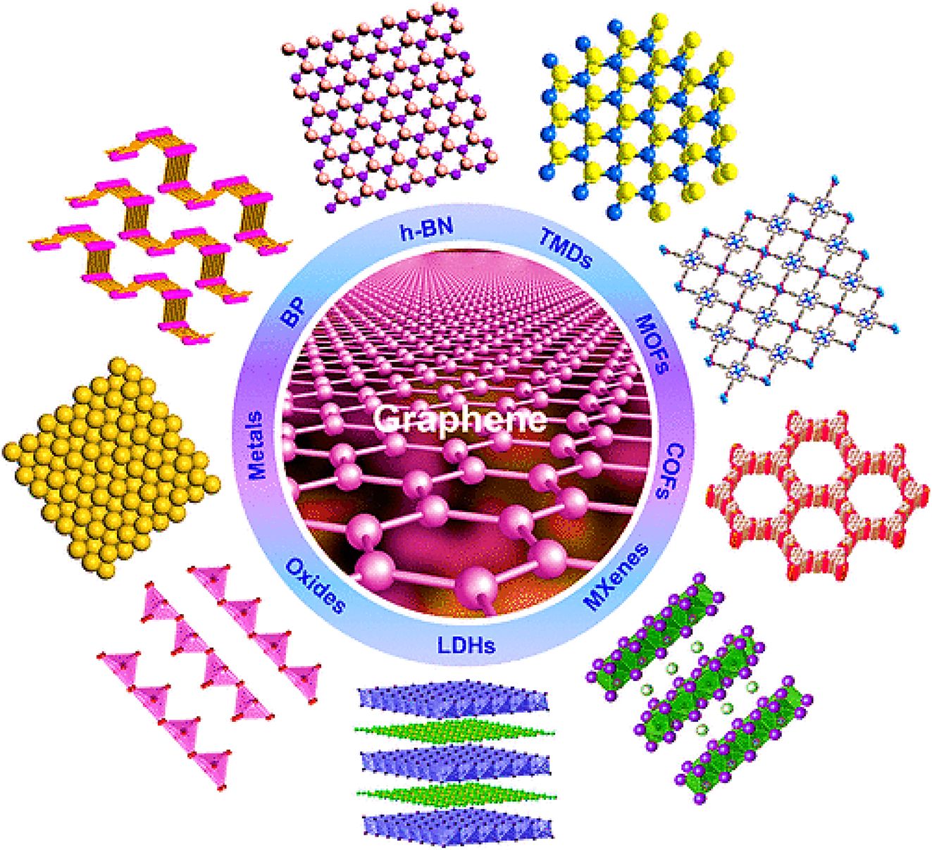
Schematic illustration showcasing various 2D nanomaterials. Reproduced with permission from 123 . Copyrights (2015), ACS.
4.1 2D materials for PSCs
Liu et al. synthesized modified PSC devices using the FTO/SnO2/Au@Nb2CTx-perovskite/MXene/Spiro-OMeTAD/Au architecture (Figure 4a). The SEM picture revealed that the thicknesses of the function layers in PSCs were 550, 45, 550, 150, and 120 nm for FTO, Au@Nb2CTxMXene-modified perovskite, SnO2, Au layers, and Spiro-OMeTAD, respectively. Figure 4b shows the difference between the JV curves of the unmodified and Au@Nb2CTx-MXene devices. The regulating unit has the following specs: Voc = 1.187 V, Jsc = 22.87 mA cm2, FF = 76.84 %, PCE = 20.86 %. The Voc of the Au@Nb2CTx-MXene-modified device was 1.215 V, the Jsc was 24.28 mA cm2, the FF was 80.62 percent, and the PCE was 23.782 percent. Backward and forward scans determine the JV curves of both unmodified and Au@Nb2CTx-MXene-modified devices. Hysteresis is minimized by inserting Au@Nb2CTx-MXene, likely due to improved surface conditions of SnO2 films and improved perovskite film quality. Figure 4c depicts the IPCE spectra of the good PSCs. The computed integrated Jsc values of 21.82 and 22.93 mA cm−2 align with the Jsc values in the J−V measurement. Additionally, the Au@Nb2CTx-MXene-modified device exhibits reduced dark current leakage compared to the control device (Figure 4d), indicating that it slows nonradiative recombination. Au@Nb2CTx-MXene passivates SnO2 substrate surface imperfections, creating a high-quality, high-crystallinity perovskite film that enhances Voc by allowing carrier movement from the layer to the ETL. Figure 3e displays electrode impedance spectroscopy spectra of control and Au@Nb2CTxMXene-modified devices without illumination. The equivalent circuit model is used to fit the EIS spectra of devices. The model includes Rs representing series resistance, Rrec representing carrier recombination, and Rtr representing charge-transfer resistance at the interface. In our scenario, device Rs values are comparable. The upgraded devices may have a lower Rtr value due to increased charge transfer speed at the perovskite/ETL interfaces. Regarding Rrec, the Au@Nb2CTx-MXene-modified device has higher carrier recombination resistance than the control device, indicating increased carrier transportation and reduced nonradiative recombination rate. This finding aligns with PL and TRPL characterizations. In Figure 4f, SCLC was measured using electron-only devices. The connection between Voc and light intensity is shown in Figure 4g. The built-in potential was determined by examining the Mott-Schottky curves (Figure 4h). Next, the control and Au@Nb2CTx-MXene-modified devices were assessed for stable current density and efficiency at maximum output power point circumstances (Figure 4i). Eventually, the device with Au@Nb2CTx-MXene upgrades shows a respectable 23.78 % power conversion efficiency and an unusually high 1.215 V open-circuit voltage (e.g., 1.60 eV). After being stored for 1,000 h in a setting with 40 % air relative humidity, the devices that were not encased showed a power conversion efficiency that was their initial value of 90 %. Furthermore, after 500 h of reaction at full power under 1 sun’s light, the device’s efficiency is still above 80 % of its original value. 124
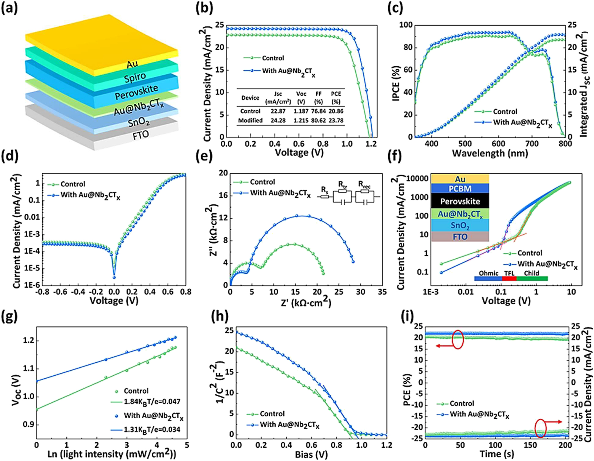
Series of measurements and analyses of perovskite solar cells (PSCs) modified with Au@Nb2CTx-MXene, including structural, electrical, and performance characteristics. (a) The incorporation of Au@Nb2CTx-MXene has modified the structure of PSCs. (b) J−V curves were measured using the reverse scan mode for both the control and the devices modified with Au@Nb2CTx-MXene. (c) The IPCE spectra of the control and PSCs were modified with Au@Nb2CTx-MXene. (d) The J−V curves of PSCs are shown, comparing those without and with Au@Nb2CTx-MXene. (e) The Nyquist plots of PSCs are displayed here, both without and with Au@Nb2CTx-MXene. (f) J–V curves illustrating the SCLC test using electron-only devices. The picture shows the structure of the devices. (g) Investigating the relationship between light intensity and the Voc of the control and Au@Nb2CTx-MXenemodified PSCs. (h) Plots depicting Mott-Schottky analysis of the control and PSCs modified with Au@Nb2CTx-MXene. (i) The current density and PCE values of the control and Au@Nb2CTx-MXene-modified devices were measured at the MPP for 200 s. 124
Huang et al. prepared the planar n-i-p perovskite solar cells, which rely heavily on interfacial engineering since it directly impacts charge extraction, transport, and photovoltaic efficiency. This study successfully developed perovskite solar cells with a high-efficiency rate using double structures of SnO2/2D TiS2 as electron transport layers. An example of a scanning electron micrograph picture of a Pero-SC segment is shown in Figure 5a. It was determined that 20 nm was the optimal thickness for the SnO2. Figure 5b depicts a schematic illustration of the energy levels. Figure 5c demonstrates the stark contrast between the forward scan (from 1.2 V to 0 V, FS) and RS curves. Using SnO2/2D TiS2 as the electron transport layer (resulted in the greatest Pero-SC PCE (21.73 %) with a Voc of 1.11 V, Jsc of 24.57 mA cm2, and FF of 79.4 %. Quantum efficiency from the outside, integrated (EQE, Figure 5d) the measured Jsc of 23.42 mA cm2 from the spectrum is quite close to the Jsc calculated from the J–V curves, demonstrating the reliability of these measurements. As shown in Figure 5e, compared to the PCE of Pero-SCs made with just SnO2, the PCE of those made using SnO2/2D TiS2 as the ETL is superior. The average PCE was 20.48 0.50 %. The PCEs of SnO2 and SnO2/2D TiS2-based Pero-SCs were also tested over time at constant voltages of 0.86 V and 0.92 V. As can be seen in Figure 5f, Average PCEs calculated from FS and RS values correlate very well with those obtained by devices using SnO2 and SnO2/two-dimensional/TiS2 as the electron transport layer. The highest power conversion efficiency was 21.73 percent, with an average of 20.48 percent (with a margin of error of 0.5 percent). In addition, the measured hysteresis was minimal. In particular, the lower densities of electron trap states and the alignment of energy levels in the ETL films are likely responsible for the increased performance. This research provided a promising interfacial material and a practical method for reducing the impact of SnO2’s trap states in planar n-i-p Perovskite Solar Cells. 125
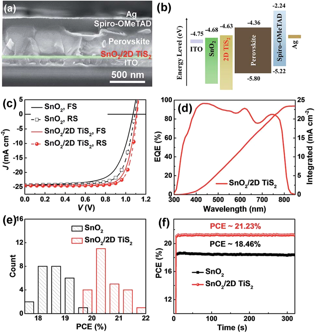
Characterization of Pero-SCs with SnO2 and SnO2/2D TiS2 ETLs. (a) Displays a cross-sectional SEM image of the Pero-SC. (b) The diagram illustrates the energy levels. (c) Representative J–V curves of the Pero-SCs with SnO2 or SnO2/2D TiS2 as ETLs are shown. (d) The EQE curve and integrated current density of the Pero-SC with SnO2/2D TiS2 as the ETL are shown. (e) Analyzing the PCE of Pero-SCs with SnO2 and SnO2/2D TiS2 as ETLs, a histogram is generated from 25 cells. (f) The steady-state efficiency of the Pero-SCs using SnO2 and SnO2/2D TiS2 as ETLs was measured under constant voltages of 0.86 V and 0.92 V, respectively. 125
Ji et al. presented the XF2 and XF3 materials, examples of a novel synthesized family of conjugated small molecule hole transport materials with better conjugation in two-dimensional orientations. Researchers used a unique technique by inserting TPA groups into the BDT unit’s side chains to control the molecule’s orientation. According to the results, the – stacking orientation was most common in two-dimensional small molecule HTMs. Through interactions involving Lewis base-acid interactions, the XF3 version, which has functionalized alkoxy groups on the TPA side chains, shows increased hole mobility and enhanced defect passivation on the perovskite surface. Since XF3 is a dopant-free hole transport material, the efficiency of an upgraded photovoltaic solar cell based on this material was 21.44 percent. After being exposed to sunlight for 840 h, the dopant-free XF3 perovskite solar cells maintained 99 % of their initial efficiency. Furthermore, when comparing devices with doped Spiro-OMeTAD to those without, it was shown that both thermal and environmental stability were vastly improved. In general, it can be demonstrated that larger conjugated side chains greatly improve the performance of hole-transporting materials. This result demonstrated the power of the 2D conjugation strategy for creating dopant-free small molecule HTMs. 126
Tang et al. reported that the perovskite layer plays a pivotal role in determining how well perovskite solar cells work. It is difficult to maintain the desired crystallinity and orientation in solution-treated perovskite films. Here, they discussed the solution-phase van der Waals epitaxy development of MAPbI3 perovskite films on MoS2 flakes. Figure 6a–d shows the position and orientation of perovskite and MoS2 atoms in their crystal structures, as determined using electron diffraction analysis. The perovskite films that develop as a consequence of this interaction have larger grains, development is favored in a direction, and rap densities are reduced perpendicular to the surface of MoS2. When the active layers are developed on top of MoS2 flakes coated on hole-transport layers, the power conversion efficiency of perovskite solar cells increases by about 15 %. Two key variables, enhanced hole extraction and transmission at the interface and improved perovskite layer crystallinity, are responsible for this improvement. Using two-dimensional materials as interfacial layers, this research introduces a revolutionary strategy for manufacturing efficient perovskite solar cells and other optoelectronic devices. 127
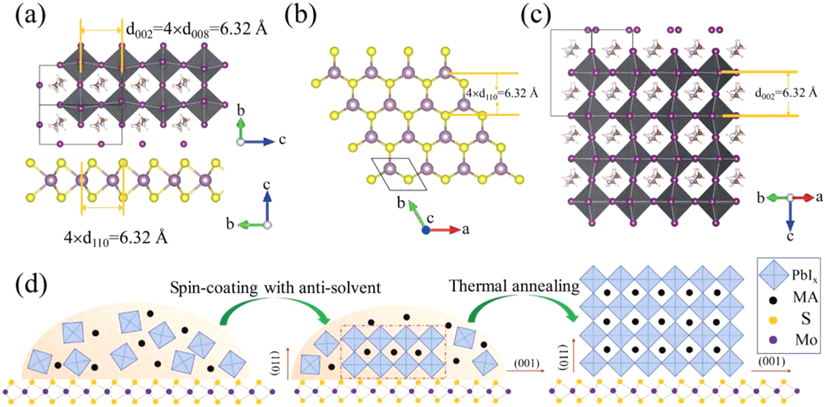
Atomic crystal structure and epitaxial growth of MAPbI3 on MoS2. (a) Shows a side view of the atomic crystal heterojunction between MAPbI3 and MoS2. (b and c) The atomic crystal structure of the (001) plane of MoS2 (b) and the (110) plane of perovskite is shown. (d) Schematic diagram illustrating the vdW epitaxial growth process of a MAPbI3 grain on a MoS2 surface.
A balanced efficiency in extracting electron transport layer interfaces, as well as PSCs-hole transport layer interactions, can be attributed to the connection between lead sulfide and the microcosmic mosaic structure present at the interface of perovskite crystals and SnS2. Suppressing charge recombination at interfaces is another benefit of this interaction. As a result, 20.12 % PCE was attained by the 2D ETL-based perovskite solar cell. Both the open- and short-circuit current densities were very high, at an astounding 1.161 V and 23.55 mA/cm2, respectively. For the advancement of high-efficiency solution-processed planar perovskite solar cells, which use two-dimensional materials, this study offers crucial background. 128 Table 2 provides a summary of various 2D materials as efficient PSC devices in recent times.
Efficient PSCs use cutting-edge 2D materials.
| Structure of device | Function | Jsc (mA cm−2) | FF (%) | Voc (V) | PCE (%) | Ref. |
|---|---|---|---|---|---|---|
| CsBr–PbI2 | PSCs | 23.394 | 71.80 | 1.030 V | 17.31 | 129 |
| ITO/SnS2/Perovskite/Spiro-OMeTAD/Au | SnS2 – ETM | 23.55 | 0.73 | 1.161 | 20.12 | 128 |
| ITO/SnO2/TiS2/Perovskite/Spiro-OMeTAD/Ag | TiS2 – ETM | 24.57 | 0.79 | 1.110 | 21.73 | 125 |
| ITO/Perovskite/PTAA/PCBM/BCP/Ag/BPQDs/ | BPQDs – active material | 21.90 | 0.83 | 1.100 | 20.00 | 130 |
| PSS/Perovskite/BPQDs/PCBM/Ag: PEDOT/ITO | BPQDs – HTM | 20.56 | 0.80 | 1.014 | 16.69 | 131 |
| Antimonene/PTAA/ITO/PCBM/Bphen/Al/PSCs | Antimonene – HTM | 23.52 | 0.77 | 1.114 | 20.11 | 132 |
| Ti3C2T x | – | 20.87 | 67.84 | 1.11 | 15.71 | 133 |
| ITO/Perovskite-MXene/SnO2/Spiro-OMeTAD/Au | MXene – active material | 22.26 | 0.76 | 1.030 | 17.41 | 134 |
| CT x -MXene-Au@Nb2 | Charge transport layer | 23.58 | 78.75 | 1.220 | 23.78 | 124 |
| ITO/MoS2/Perovskite/PTAA/PCBM/BCP/Ag | MoS2 – HTM | 22.66 | 0.80 | 1.130 | 20.55 | 127 |
| ITO/GO/Perovskite/PEDOT:PSS/PCBM/MoS2/Ag | Graphene oxide – HTM; MoS2 – ETM | 22.83 | 0.74 | 1.135 | 19.14 | 135 |
| Spiro-OMeTAD | HTMs | 24.24 | 78.65 | 1.08 | 21.44 % | 126 |
| SnO2–Ti3C2/ITO MXene/Spiro-OMeTAD/Ag/PSCs |
MXene – ETM | 23.14 | 0.75 | 1.060 | 18.34 | 136 |
| FTO/TiO2–phosphorene/Perovskite/Spiro-OMeTAD/Au | Phosphorene – ETM | 23.32 | 0.71 | 1.080 | 17.85 | 137 |
5 3D materials
The architectures of 3D nanomaterials are characterized by the presence of linked macro/mesopores, which effectively hinder the processes of aggregation and restacking. This nanomaterial has the most accessible surface area compared to other nanomaterials. Several scholarly sources have shown further benefits of 3D nanomaterials. 138
Macro and mesoporous channels facilitate the exposure of internal surfaces and enable the entry of molecules and ions into the empty spaces. This facilitates the use of applications such as catalysis, medication delivery, sensing, and other related fields.
The presence of a porous structure facilitates a significant increase in the loading capacity of functional components, such as catalyst particles or medicines.
The presence of pores gives rise to confinement effects, which can influence chemical and physical characteristics.
An inner empty space facilitates the transportation of mass inside the three-dimensional structure.
The three-dimensional morphology of nanoparticles enhances their mechanical stability compared to nanomaterials with one-dimensional or two-dimensional structures.
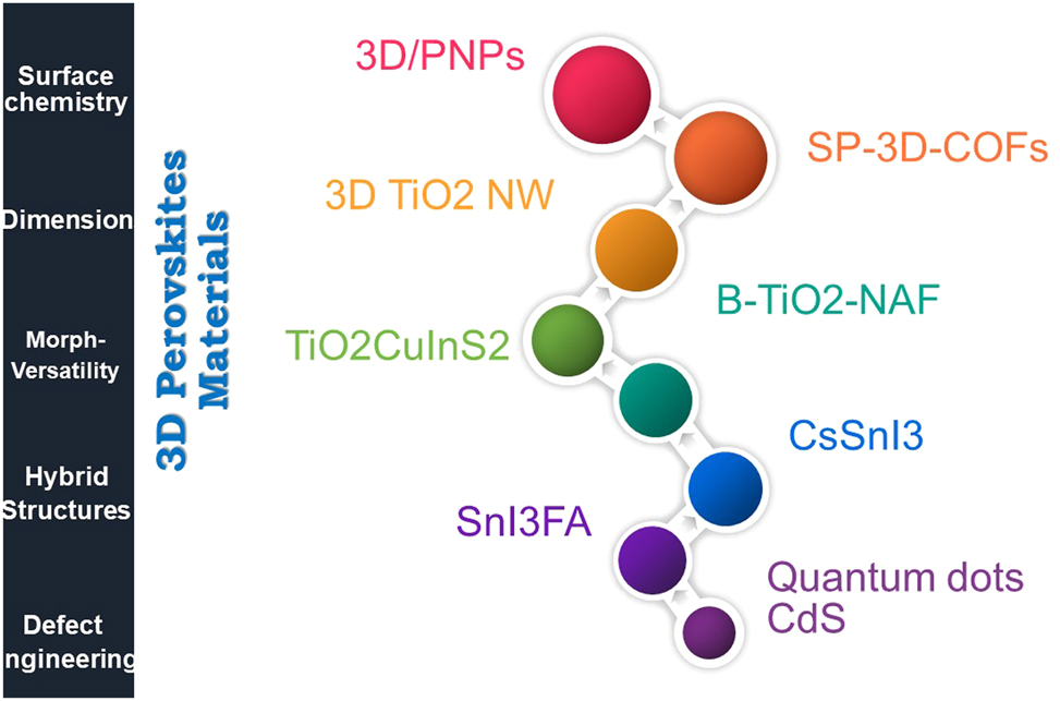
Further points of comparison regarding the structural merits of 3D nanomaterials with alternative dimensionalities include the following (Figure 7). 139 , 140 , 141
Structural properties modification of 3D materials.
Surface chemistry: The expansive surface area shown by 3D nanomaterials affords enhanced prospects for customizing surface chemistry through functionalization. There is an increased availability of binding sites that can be modified with target molecules.
Dimensions: The dimensionality of nanomaterials may be effectively controlled, allowing for the intentional construction of three-dimensional structures with precise macro/mesoporosity and interconnected pores. This enables the adjustment of the three-dimensional configuration to achieve certain characteristics.
Morphological versatility: The morphological plasticity of 3D nanomaterials allows for their synthesis in a diverse range of forms, including spheres, tubes, and gyroids, among others. This enables the process of optimizing forms to suit various purposes.
Hybrid structures: Hybrid structures are characterized by their three-dimensional porosity network, which facilitates the integration of various components to generate hybrid nanomaterials. An instance of this would be the integration of 3D graphene with metal nanoparticles.
Defect engineering: Defect engineering refers to deliberately manipulating flaws in 3D nanomaterials to control and modify their reactivity. The increased surface area in these nanomaterials offers a greater scope for implementing defect engineering strategies.
In brief, these nanoparticles’ distinctive three-dimensional porous structure confers significant benefits, including a substantial accessible surface area, adjustable void spaces, improved mass transmission, high loading capacity, and exceptional mechanical stability. These advantages provide a wide range of applications across several disciplines. Moreover, the distinctive architectural benefits of 3D nanoparticles provide enhanced structural manipulation, multifunctionality, synergistic effects, processability, and optimization of performance in comparison to nanomaterials of various dimensionalities.
5.1 3D materials for PSCs
Zhang et al. demonstrated that a 3D structured perovskite, namely (MePDA)Pb2I6, may be used as a surface-modification layer on top of a more typical 3D perovskite material. In Figure 8a and b, under simulated one-sun (AM 1.5 G) illumination, both the unmodified and Me-PDAI2-enhanced PSCs’ photocurrent density-voltage curves are shown, with the relevant PV parameters listed in the insets. Figure 8c shows that the Jsc values from the J–V observations are in excellent agreement with the external quantum efficiency spectra that correspond to the integrated current densities. Figure 8d shows the stabilized power outputs, which are in good agreement with the J–V measurements, at 20.1 % and 21.8 % for the unmodified and Me-PDAI2-modified PSCs. Un-encapsulated PSCs have a shelf life of two to four years in room temperature air with a relative humidity of 20%–40 %, as shown in Figure 8e. Me-PDAI2-modified PSCs had a 90 % reduction in PCE after 1,008 h, whereas control PSCs had a 22 % decrease. Maximum power point tracking in N2 is displayed in Figure 8f, in addition to the results of ISOS/L stability testing on devices without enclosures in normal use conditions. Perovskite thin films had improved features after having their top layer, generated as the initial three-dimensional perovskite, transformed into a perovskite. The enhanced carrier lifetimes, enhanced carrier motilities, and decreased surface defect densities demonstrate this enhancement. They increased the device’s effectiveness from around 20 %–22 % using the aforementioned way while also maintaining its steadiness. After 500 h of maximum power point monitoring under constant one-sun illumination, 90 % of the device’s initial value remained intact. Several other types of perovskite compositions, i.e., FAMA-, Perovskites of lead halides based on MA, and CsFAMA– have been shown to benefit from the surface engineering method we have described. 142
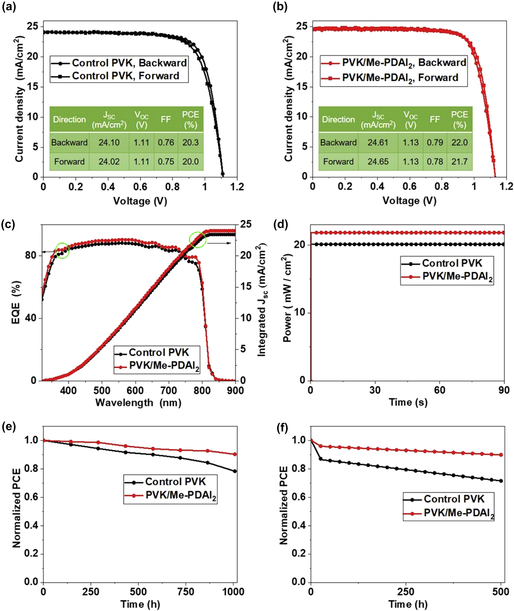
J–V curves of PSCs using the (a) control and (b) Me-PDAI2-modified perovskite films. (c) (d) EQE spectra and integrated current curves of the corresponding devices and SPO. (e) (f) Comparing the stability of shelf ISOS-D−1 at room temperature with 20%–40 % relative humidity and the stability of operation ISOS-L−1. 142
Zhu et al. presented that perovskite nanopillars can replace thin films in flexible photovoltaic applications because of their advantageous properties for solar energy absorption, as shown in Figure 9a–e. To maximize daily energy output, photovoltaic systems must absorb light from the sun at a broad range of incidence angles and in the whole spectrum of usable wavelengths. A comprehensive evaluation of core-shell-based 3D PNP-based flexible photovoltaics was performed. At their peak performance, the vertically oriented PNP arrays absorb at a rate of 95.70 and 75.10 percent, respectively, when the incidence angle is set to 60°. Broadband wavelength external quantum efficiency is improved by efficient absorption and orthogonal carrier collecting techniques to a range of 84.0%–89.18 %. PNPs have been successfully used in flexible solar cells. With a porous alumina barrier protecting PNPs from oxygen and water, photovoltaic systems may last longer and be less likely to break down. Novel PNP-based technology has extraordinary mechanical stress and strain resistance enabling efficient solar-to-electricity conversion even when bent. 143
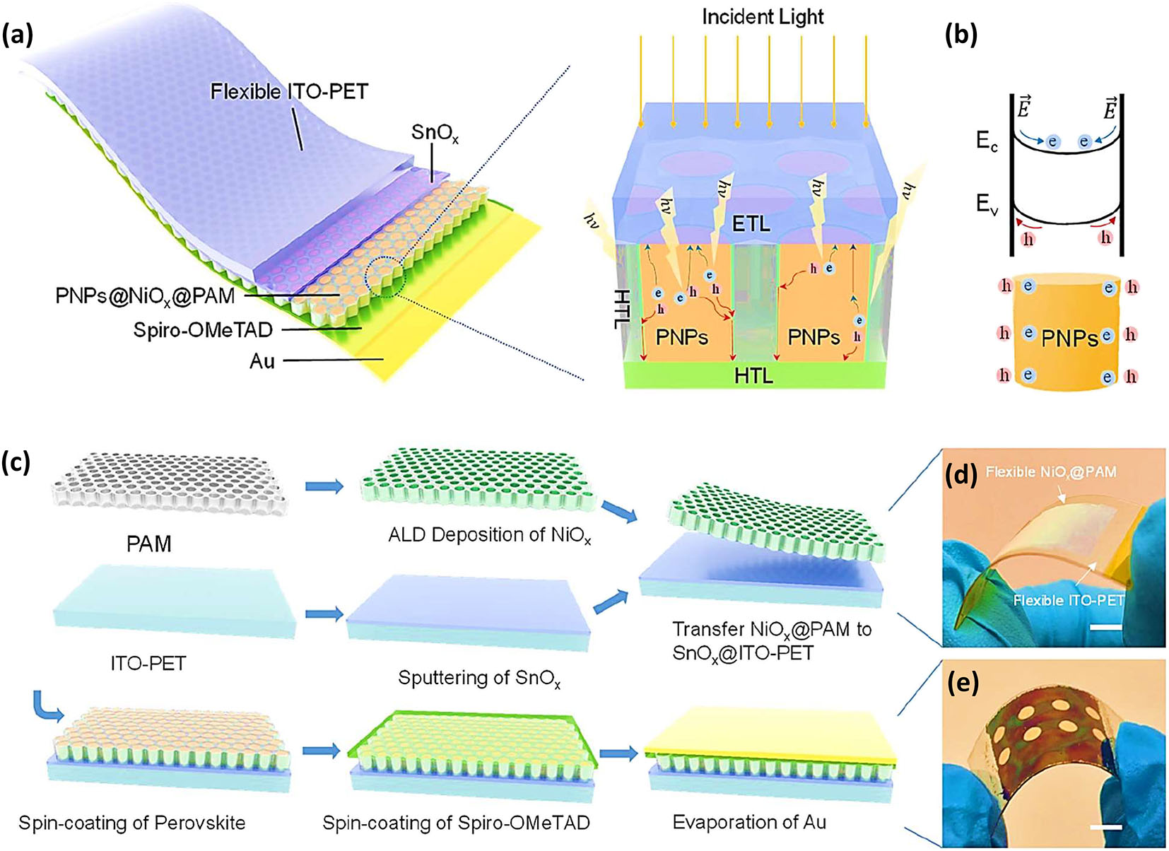
Structure, fabrication, and implementation of PNP-based solar cells. (a) Complete structure diagram and cross-sectional schematic diagram of PNP-based solar cells. (b) The schematic band structure of the PNP crystal surface showcases the formation of a built-in electric field. (c) A schematic illustration depicting the fabrication procedure for PNP-based devices. (d) Photographs showing the implementation of NiOx-coated PAM (NiOx@PAM) on the SnO2-coated ITO-PET (SnO2@ITO-PET) and (e) the complete device. 143
Chen et al., 2022 synthesized by using a post-treatment, a one-dimensional PbI2(Phen) adduct phase was successfully incorporated into a three-dimensional perovskite. The structural and optoelectronic features of the underlying three-dimensional film were not noticeably altered by the presence of a one-dimensional structure on surface. The passivation of the surface of the 1D-3D perovskite film led to a reduction in trap density compared to the 3D perovskite film. In a three- and one-dimensional perovskite solar cell, the greatest power conversion efficiency ever reported was 23.3 %. The perovskite film showed improved endurance in a range of environmental conditions when made of several components. For 1D structures, the protective covering performed a dual purpose as a capping against ion movement. The one-dimensional/three-dimensional structural photovoltaic device was more stable than its three-dimensional counterpart because of its simpler design. This research shows that mixed-dimensional engineering may be used to make superior perovskite films, which might hasten the development of perovskite solar cells for a wide range of uses. 144
Gao et al., 2023 stated that due to its excellent performance features, a lot of people are interested in the organic-inorganic hybrid perovskite solar cells that have been developed lately as a potential new direction for next-generation photovoltaic systems. However, the interfacial stability of these materials is poor, which limits their marketability. Improving stability is a major area of focus in the sciences today. The purpose of this research was to find a solution to this problem by synthesizing a bilayered titanium dioxide nanorod array-flower for use in hybrid perovskite solar cells as an electron transport medium. The lowered electron trap density, reduced carrier recombination resistance, improved electron injection, and reduced nonradiative recombination rate all contribute to the B–TiO2-NAF device’s impressive 21.8 % power conversion efficiency. The internal photoexciton diffusion distance is decreased when B–TiO2-NAF is used because it provides a uniform D/A interface in all three dimensions. With an efficiency that remains at over 83 % after 30 days, the gadget clearly exhibits outstanding long-term stability. Our study’s findings might aid in the development of 3-D semiconductor materials and provide new light on how to improve the durability of perovskite solar panels. 145
Jing et al., 2022 presented the growing single crystal anatase three-dimensional-TiO2 electron layer transport on FTO substrates hydrothermally using a TiF4 solution, which has shown to be an efficient method. When compared to devices using carbon-TiO2 electron transport layers produced with TiCl4 solution, the photovoltaic performance of CsPbIBr2 perovskite solar cells employing 3D-titania electron transport layers is dramatically improved. When a three-dimensional titanium dioxide electron transport layer is added to a CsPbIBr2 perovskite solar cell, the power conversion efficiency may reach 10.65 percent. The device employing the widely used Spiro hole transporter and gold electrode produces a PCE of 10.79 %, making this PCE similar. Furthermore, the power conversion efficiency of the CsPbIBr2 PSC with 3D-TiO2 ETL is much greater than that of the device, including a titanium dioxide ETL made using a titanium tetrachloride solution, which reaches 8.38 %. In particular, the three-dimensional titania electron transport layer is effective in blocking harmful ultraviolet light. This quality effectively counteracts the main shortcoming of conventional TiO2 ETLs, which is their sensitivity to ultraviolet light. This makes it easier to create cesium lead iodide bromide perovskite solar cells, which are very resistant to the effects of sunlight. Not only are devices with 3D-TiO2 electron transport layers resistant to dampness and heat, but they also perform well in these environments. Therefore, the use of 3D-TiO2 ETLs might be a promising strategy for the development of high-performance and long-lasting all-inorganic perovskite solar cells. 146 Table 3 provides a summary of various three-dimensional materials as efficient PSC devices in recent times.
3D material-based for perovskite solar cell.
| 3D material | Band gap | PCE (%) | Voc (V) | FF (%) | Jsc (mA cm−2) | Main approach | Ref. |
|---|---|---|---|---|---|---|---|
| ITO/SnO2/perovskite/Spiro-OMeTAD/Ag | 2.51 | 23.3 | 1.08 | 80.7 | 24.9 | Two-step deposition method | 144 |
| SnI3/FA | – | 10.81 | 0.69 | 75.00 | 21.59 | Iodine-pentafluorobenzene-oxyethyl ester | 147 |
| SP-3D-COFs | 16.70 | 1.028 | 72.1 | 22.50 | Annealing | 148 | |
| Me-PDAI2 | 22.0 | 1.00 | 90.3 % | 52.8 | Vapor deposition | 142 | |
| 3D/PNPs | – | 89.18 | 0.97 | 79.01 | 21.19 | Two-step anodic anodization method | 143 |
| 3D-TiO2NW | – | 4.0 | 0.71 | 0.63 | 12.2 | PCVD with a restricted surface reaction rate | 149 |
| B–TiO2-NAF | – | 21.8 | 1.11 | 82 | 23.1 | Electrochemical deposition | 145 |
| FA/SnI3 + Br/PEA | – | 14.63 | 0.91 | 77.10 | 20.60 | Single-step SnI2.DMSO synthesis | 150 |
| CsPbBr2/TiO2/PSCs | 2.3 | 25.5 | 2.01 | – | – | Hydrothermal | 146 |
| SnI3FA0.75 MA0.25 | 1.37 | 10.30 | 0.63 | 75.50 | 21.62 | Vacuum treatment | 151 |
| Quantum dots CdS | 2.25 | 8.50 | – | – | – | Grafting route | 152 |
| FA0.75SnI3 MA0.25 | 1.31 | 9.26 | 0.58 | 72.81 | 21.93 | Hydrazine dihydrochloride additive | 153 |
| CsSnI3 | 1.31 | 10.10 | 0.64 | 72.10 | 21.81 | Band alignment by localized electron engineering using a phthalimide additive and an indene-C60 disadduct | 154 |
| FAI3Sn | 1.40 | 7.53 | 0.53 | 65.80 | 21.80 | Polyethylene glycol scaffold | 155 |
| SnI3FA | 1.35 | 7.40 | 0.60 | 65.00 | 16.45 | Iodine-pentafluorobenzene-oxyethyl ester | 156 |
| FA0.75SnI2MA0.25Br | – | 6.02 | 0.56 | 65.00 | 16.66 | Catechin dopant/antioxidant | 157 |
| GeI2doped (EA0.1FA0.90)SnI3 EDA0.01 | 1.42 | 13.24 | 0.84 | 78.00 | 20.32 | GeO4 surface passivation, bandgap alignment by EA doping, and protection | 158 |
| TiO2CuInS2 | 1.55 | 5.0 | 0.53 | 0.55 | 17 | Chemical spray deposition | 159 |
| FA0.75SnI3 MA0.23 |
1.36 | 11.50 | 0.76 | 69.00 | 22.00 | Sn nanoparticles in a precursor solution, and then EDA and PC61BM were applied to their surfaces. | 160 |
6 2D/3D heterojunctions
The formula for 2D-3D multi-dimensional mixed-halide perovskites is M2An 1BnX3n + 1, where M is an inorganic cation such as methylammonium/formamidinium/Cesium; A is an organic cation such as methylammonium/formamidinium/Cesium; B refers to tin or lead; halide anion represents by X (Cl, Br, or I); and n = number of metal halide sheets, whereby the solution’s precursor composition is used to roughly predict n values. 161 For 3D perovskites, n = ∞ is the limit, but for 2D halide perovskites, n = 1 is the case. In phase-pure crystals containing n-member perovskite, the decrease in thermodynamic stability of larger n-members as n increases has a profound effect on the development of specific n-layer isolation in the pure form and can even lead to the mixture of products. 162 It is worth noting that for large n values, such as n = 30, 40, 50, or 60, a mixture of low n-member phases (n 3) and 3D perovskites may form owing to the presence of organic/inorganic molecules as a spacer. It is difficult to get exceptionally pure samples by devising in situ processes due to the kinetically rapid, self-assembled, and controlled nature of n-membered perovskites during the thin-film production from the solution process. Therefore, such 2D-3D perovskites are often described by their M-molar percentages, as in M/(A+ M), rather than by n numbers. 163
Conventional PSCs, such as a perovskite-perovskite heterojunction, were modeled using device physics to examine chemical- and field-effect passivation processes. They found that a 0.2 eV energy offset (bi) for the perovskite junctions significantly improves the interface’s defect tolerance, requiring less preparation time and effort. Figure 10a displays photovoltaic characteristics and J–V curves for the best devices in each category of PSCs. The control PSC’s PCE, Jsc, Voc, and FF are all below 80 %. The control PSC’s Voc is just 1.120 V. The BABr and BAI PSCs have a high PCE (24.16 % and 25.32 %), a low V OC (1.134 and 1.159 V), and a remarkable FF (81.8 % and 83.2 %). At a constant rate of change, the PCE for these three was 22.57 %, 23.84 %, and 25.04 %. Success in achieving a PCE of 25.32 (Figure 10b and c) is an all-time high for 2D/3D perovskite-based PSCs. An authorized lab confirmed it by testing a BAI-based 2D/3D PSC. Figure 10d displays the results of the tests, which revealed a PCE of 25.04 %, a high Voc of 1.152 V, a wonderful Jsc of 25.986 mA cm2, and a fantastic FF of 83.68 %. By monitoring the devices’ output power under constant illumination (100 mW cm2) and at MPP circumstances, we could gauge the reliability of their long-term functioning. In under 100 h (T80), the PSC in the control group had degraded to 80 % of its original PCE. The T80 stability of a PSC based on BABr with 2D/3D heterojunctions was increased to 500 h. Notably, after 2000 h of operation (T90 = 2000 h), 90 % of the original values of BAI-based PSCs with 2D/3D heterojunctions remained unchanged. They were also employed to build PSC modules to investigate the perovskites’ performance in large-area devices (Figure 10f). Figure 10g shows that the best BAI-based PSC module achieved a Jsc of 2.83 mA cm2, an FF of 80.3 %, a Voc of 9.416 V, and a PCE of 21.39 %, while the average PCE of 16 PSC modules exhibited comparable improvements in PCE (Table 4).
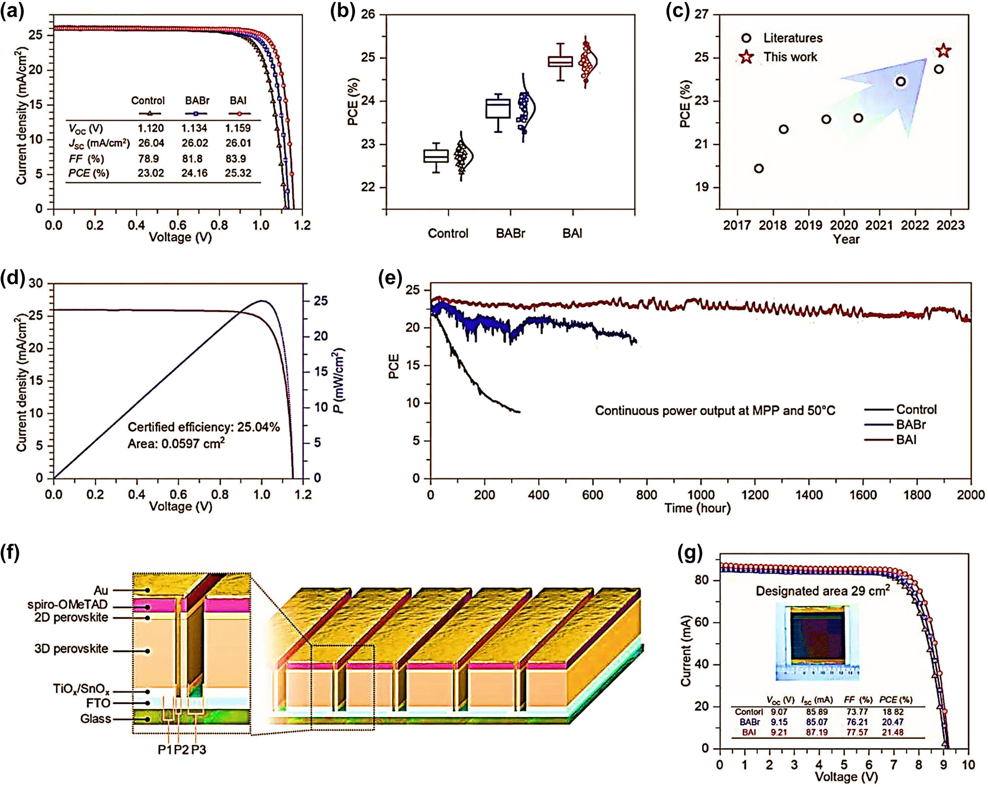
Performance and characterization of 2D/3D PSC devices and modules. (a) Highlighting the impressive performance of the 2D/3D PSC devices and modules. Graph showing the J–V curves of the champion cells. (b) PCE statistics of 34 cells for each type. (c) Displays the power conversion efficiencies of 2D/3D perovskite-based photovoltaic solar cells (d) J–V and P–V curves certified by the Photovoltaic and Wind Power Systems Quality Test Centre, IEE, Chinese Academy of Sciences for the BAI-based 2D/3D heterojunction PSCs. (e) Photovoltaic cell efficiency of the photovoltaic solar cells under continuous illumination at maximum power point operating conditions. (f) A schematic of the PSC modules with nine sub-cells connected in series. (g) Graph showing the J–V curve of the champion PSC modules tested with an aperture mask of 29 cm2. 164
PSCs based on 2D-3D mixed-perovskite absorbers and their efficiency and stability.
| Perovskite | Voc/V | FF | PCE% | Jsc/mA cm−2 | Stability | Device structure | Ref. |
|---|---|---|---|---|---|---|---|
| PSCS-MEMI | 1.106 | 0.802 | 22.41 | 25.27 | 7.5 % after aging in the dark air condition for 300 h | FTO/TiO2/Rb0.02(FA0.95Cs0.05)0.98PbI2.91Br0.03Cl0.06(3D)/2D-PVK/Spiro-OMeTAD/Ag | 165 |
| PbI2:MAI:AnI (1:0;8:0.2) | 1.04 | 0.60 | 15.96 | 25.55 | NA | ITO/PEDOT:PSS/perovskite/PCBM-61/BCP/Ag | 166 |
| (BzDA)(Cs0.05MA0.15FA0.8)9– Pb10(I0.93Br0.07)31 (n = 10) | 1.02 | 0.71 | 15.6 | 21.5 | 80 percent PCE in 84 h of darkness and 20–50 percent RhB | TiO2/m-TiO2/PVK/FTO/c/spiro-OMeTAD/Au | 167 |
| MA39CA2Pb40I121 (n = 40) | – | – | 6.6 | – | After 264 h in the dark at 77 % RH, PCE is 59 %. | PVK/SnO2/spiro-OMeTAD/ITO/Au | 168 |
| Gua0.1/Pb(I0.83Br0.17)3/[Cs0.1(FA0.83MA0.17)0.9]0.9/ | 1.19 | 0.75 | 21.21 | 23.66 | 100 % OF PCE after 500s | ITO/SnO2/PVK/spiro-OMeTAD/MoO3/Ag | 169 |
| (DA2PbI4)0.05MAPbI3 | 1.05 | 0.79 | 19.09 | 22.95 | After 60 days, 80 % of PCE is in the dark. | spiro-OMeTAD/TiO2/PVK/ITO/MoO3/Ag | 170 |
| [Pb(I0.83Br0.17)3) (FA0.83MA0.17)Cs0.05] | 1.1 | 79.68 | 20.23 | 23.08 | A PCE of 21.4 % and excellent background air condition consistency over 1,000 h | – | 171 |
| 0.91Pb(I0.6Br0.4)3 BA0.09(FA0.83Cs0.17) | 1.18 | 0.73 | 17.2 | 19.8 | After 1,000 h in the dark and air, 80 % PCE | SnO2/FTO/PC61BM/spiro-OMeTAD/PVK/Au | 172 |
| FA/MA/Cs | 1.085 | 79.2 | 19.8 | 23.3 | 25 % of PCE after 5,000 h under illumination and in dark | – | 173 |
| (AVA2PbI4)0.03(MAPbI3)0.97 (Cell) | 0.857 | 0.59 | 23.60 | 10.10 | PCE reached 100 % after 10,000 h at 55 °C with continuous light exposure | FTO/TiO2/ZrO2/PVK/C | 163 |
| PEI2PbI4)x(MAPbI3)1 − x | 1.11 | 0.67 | 11.01 | 15.01 | 78.5 % after 160 h in RH 55 % | PEDOT/ITO/Ag:PSS/PVK/BCP/PCBM | 174 |
| PSCs-PTAA | 1.125 | 25.96 | 24P.6 % | 84.32 | Initial PCE of under LED light and N2 environment | – | 29 |
| ACI | – | – | 22.26 | – | 93.81 percent PCE over 1,200 h at 25 degrees C and 25 % relative humidity. | TiO2/PVK/spiro-MeOTAD/Au-FTO/c | 175 |
| PbnI3n + 1 (BA)2(MA)n − 1 | 1.11 | 0.78 | 19.56 | 22.49 | 96.5 % at 95 °C in the absence of light after 100 h | PTAA/Cu/PVK/ITO/PCBM/C60/BCP | 176 |
| Cs0.05MA0.05FA0.9PbI3 and spiro-OMeTAD | 25.32 | – | 90 % PCEs after 2,000 h of continuous under 1 sun | 9,9′-spirobifluorene-2,2′,7,7′-tetrakis[N,N-di(4-methoxyphenyl)amino] | 164 | ||
| PSCs-TFPhFACl | 1.16 | 81.26 | 25.7 | 25.42 | Airborne PCE 14.78 % after a storage period of 1,500 h | – | 177 |
This study uses 4-(trifluoromethyl) benzamidine hydrochloride to create a 2D capping layer on top of 3D perovskite. Two recognized channels work together to boost output: (1) The dipole layer created by the TFPhFA+ cations facilitates the transport of charges across the contact. (2) The coordination of TFPhFA+ cations with the Pb–I octahedron induces recrystallization of 3D perovskite and suppresses nonradiative recombination of perovskite. These upgrades allow the PSC to operate at a 24.0 % efficiency, 1.16 V open-circuit voltage, 25.42 mA cm−2 short-circuit current density, and 81.26 percent fill factor. After being exposed to air for 1,500 h, the gadget still functions at the same efficiency level as when it was first used. The crystal grains in 3D perovskite film are scattered randomly, as seen in Figure 11a–d. The buildup of 2D perovskite in the valley region of 3D perovskite is seen after treating the material at a low concentration of 2.5 mg m/L. Furthermore, as shown in Figure 11e and f, the lamellar-structured portions of the 3D perovskite surface vanished, and the grain boundaries became more defined. This data implies that TFPhFACl recrystallizes into 3D perovskite after being subjected to a surface treatment. At high concentrations of 5 and 7.5 mg m/L, mixed 2D/3D perovskite occurs, making it difficult to distinguish the surface morphologies of underlying 3D perovskite layers. Comparison of cross-sectional images of untreated and TFPhFACl-treated perovskite films at a concentration of 5 mg m/L. 177
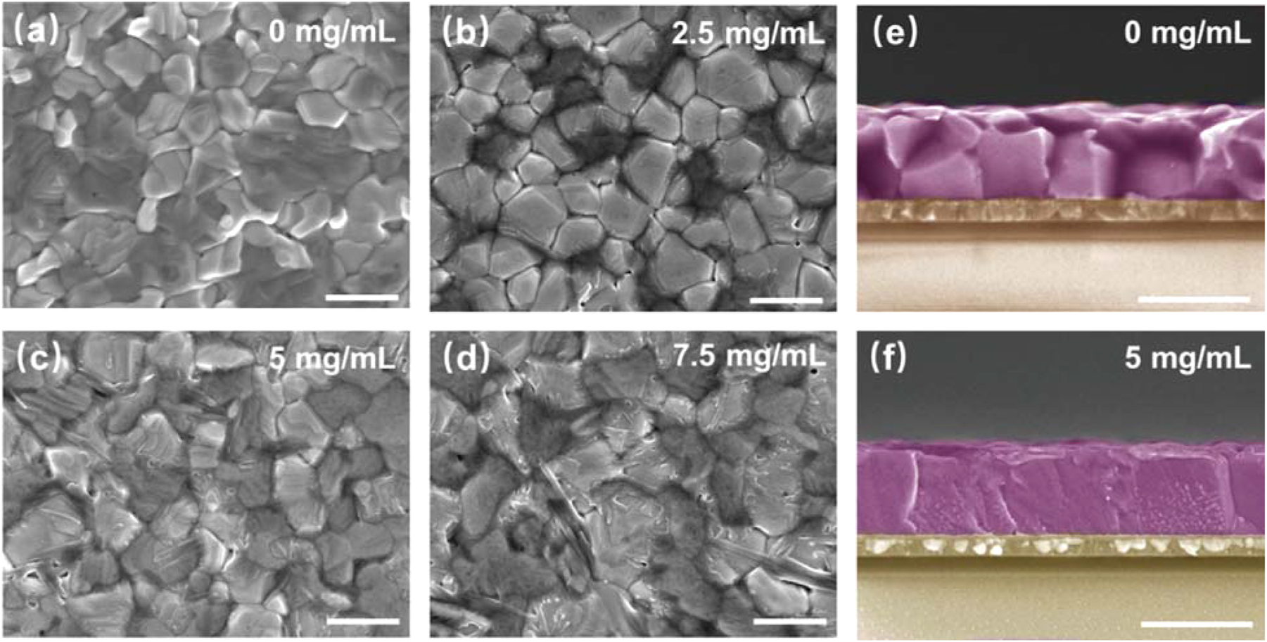
Morphological analysis of TFPhFACl-treated and untreated perovskite films with varying concentrations of TFPhFACl. (a–d) Morphology pictures of TFPhFACl-treated and untreated perovskite films. Perovskite films with varying amounts of TFPhFACl were photographed on their surfaces and in cross-section (e and f). The scale bar is 1 μm.
7 Application of PSCs
7.1 Solar-powered catalysis
Solar-powered catalytic processes for chemical synthesis are promising and environmentally friendly. Advanced catalytic technologies like water splitting and CO2 reduction might economically deliver clean energy and industrial raw materials. Solar catalysis includes photocatalysis, photoelectrochemical catalysis, photothermal catalysis, and photosynthetic reactions. Much scholarly research has been published to fully understand solar-driven catalytic reactions. 178 , 179 , 180 Water splitting and carbon dioxide reduction processes will be covered in this review. The water splitting and CO2 reduction catalytic properties of PSC cells are highlighted in this paragraph.
7.1.1 PSC-driven water splitting
Hydrogen energy, sometimes called H2 fuel, is a proven zero-carbon fuel with promising applications in fuel cells with internal combustion engines. Hydrogen energy can be transferred via existing natural gas pipelines and stored in a gaseous form at high pressures. Hydrogen production by water electrolysis is seen as a promising green technology. Electrolysis is a method that uses an electric current and a suitable electrode to separate hydrogen and oxygen from water. An effective electrocatalyst and a high-voltage PV-electrolyzer are crucial components in water electrolysis. To split water with the least amount of energy, the 1.23 V potential is suggested to represent the thermodynamic equilibrium. The actual working potential might be anywhere from 1.5 to 2.0 V. 181 The high working voltages of an electrolyzer need a series of connections between individual cells or several junctions. 182 It is anticipated that connecting two PSC modules would be adequate to generate the open-circuit voltage levels of perovskite solar cells, which are high enough for water splitting to occur, are often more than 1.0 V. Using perovskite solar cells as an electrolyzer to split water, a team of scientists led by its leader made a significant discovery in 2014. 183 CH3NH3PbI3 was utilized to connect two separate perovskite solar cells. The open-circuit voltage of PSCs was 1.06 V, and their efficiency in converting electricity was 17.3 %. The module’s open circuit voltage reached 2.00 V by connecting the two cells in series, which is more than enough to facilitate effective water splitting.
A solar-powered water-splitting system benefits significantly from using high-voltage solar cells because they are economical and effective. Perovskite solar cells made entirely of inorganic materials and bromine-based cells with a single connection are two promising options worth exploring. Perovskite tandem photovoltaic devices have attracted significant attention for their potential integration into a wide range of applications. To produce H2 and O2, graphene-based materials were used as catalysts in the first example of hybrid PTSC-driven water-splitting. 184 The 1.86 V shown by the tandem cell’s Voc was enough for water splitting. The real STH effectiveness was below 10 %, unfortunately. After being run for more than 2 h, STH’s conversion efficiency declined dramatically to 18.02 %. The significance of this conclusion lies in the fact that it predicts continued stability for the system. The enhancement of photovoltaic performance in tandem solar cells and the development of efficient bifunctional electrocatalysts are two areas where further advancements in this category of integrated systems are expected.
7.1.2 PSC-driven CO2 reduction
For a long time, researchers have tried to figure out how to employ catalysis to convert CO2 into chemical feedstocks and fuels effectively. The manufacture of high-value chemicals relies on this technique, and it also has the potential to lessen the impact of human-caused global warming by carbon dioxide emissions. One potential approach to effectively use these abundant resources is the carbon dioxide reduction process, which employs renewable power generated from solar energy. Although energy can be generated by single-junction solar cells, the driving voltages needed for CO2RR are much higher. More precisely, the output voltage of the PV cell must be more than 2.0, 181 which again necessitates a series connection of single-junction PV cells. Researchers used 3.10 V of Voc by series-connecting three single-junction PSCs to convert CO2 to CO. 185 The oxygen-evolution catalyst in this study was iridium oxide, while the cathodic carbon monoxide-evolution catalyst was gold. Using two parallel groups of three triple-cation PSCs, the same CO2 to hydrocarbon conversion was accomplished. 186 Recently, an electrochemical cell with copper and ruthenium dioxide electrodes was successfully used to convert light-driven CO2 to methane with an efficiency of 5 %, using a solar-to-fuel conversion efficiency. 187
Multi-junction PSCs are expected to be used for high-efficiency, low-cost CO2 conversion because of the high driving voltages necessary for CO2RR. Many groups have reported very efficient perovskite triple-junction solar cells, but to the best of our knowledge, nobody has tried to optimize these cells for carbon dioxide capture, storage, and re-use. Tan’s team achieved Voc values of 2.80 V in monolithic PSCs triple-junction solar cells. 188 By integrating three perovskites with different bandgaps (1.99 eV, 1.60 eV, and 1.22 eV), this triple-junction device exemplifies how the properties of a single perovskite device may be adjusted to an application with stringent parameters, such as CO2RR.
7.2 Solar photovoltaic energy storage
As a result, solar cells as a unit of energy conversion and storage have emerged as a potentially game-changing strategy for advancing renewable and clean Technology. The Technology for storing energy includes lithium-ion batteries, supercapacitors, hydrogen fuel cells, and other rechargeable batteries because of their power density, extended lifespan, and high energy. 189 Despite this interest, the overall performance of systems that combine energy storage with various solar cell technologies, such as organic photovoltaic cells and DSSCs, remains unsatisfactory, primarily because solar cells only produce a small amount of power efficiency energy. 190 , 191 Therefore, much recent development has been in incorporating PSCs into the setup. Devices for converting energy and storing it must be integrated. Their voltages must be matched. Because of their high Voc values, PSCs are often considered a top contender for use in energy conversion and storage applications.
7.2.1 PSCs–supercapacitors
Supercapacitors have various advantages over other energy storage systems. Some benefits are high power densities, fast charging and discharging, and ultralong cycle stability. In combination with solar panels, supercapacitors provide a compelling alternative because of their low voltage requirements. 192 For the first time, a CH3NH3PbI3-based PSC has been used to power a supercapacitor comprising cellulose membrane, polypyrrole nanofibers, and multi-walled carbon nanotubes. The total efficiency was determined by analyzing the relationship between the charging time, the amount of active area, and the light intensity. Such efficiency is remarkable compared to integrated systems built using other solar cell technologies. The primary constraint of this study was the very lengthy charging period of 300 s caused by the difference between supercapacitor and PSC active areas. The device’s larger active surface area may allow for faster capacitor charging. By integrating a graphene-based strain sensor, a lithium-ion capacitor module, a flexible lithium-ion capacitor, and a flexible photovoltaic solar cell, Liu’s team created a self-powered wearable sensing system. 193
Photo-supercapacitors, which combine a PSC with a supercapacitor, have gained popularity in recent years owing to their feasibility as a sustainable, on-the-go energy solution. The issue is that the input and output voltages of this wire-free integrated device must be very high. Four photo-supercapacitors were linked in sequence to provide a consistent 3.8 V. 194 LEDs were driven by the power pack, which was recharged using photovoltaic cells, showcasing the versatility of this cutting-edge technology. Since high voltages are required by supercapacitors, high-efficiency PTSCs created by fusing PSCs with supercapacitors are an attractive option for solar-rechargeable supercapacitors.
7.2.2 PSCs–batteries
The broad use of “smart” technology, such as smartphones, electric vehicles, and smart grids, is a major betting point for many. These cutting-edge technologies currently rely primarily on energy storage in the form of rechargeable batteries. Due to their high energy densities and outstanding chemical stabilities, metal-ion batteries (such as LIBs) are often utilized as the energy storage units of solar rechargeable batteries. The compatibility of lithium-ion batteries with Si-based multi-junction solar cells and DSSCs has been shown in previous publications. 195 , 196 However, most energy conversion devices (solar cells) have an output voltage of less than 0.8 V; therefore, they cannot be used to power energy storage devices. Many PV units must be paired in series to produce high enough output voltages, which is counterintuitive to the design of tiny, integrated systems. Solar-powered rechargeable batteries may benefit from the usage of high-voltage PSCs.
Lithium-sulfur batteries are competitive because of their high energy density and low weight. Their 2.8 V cutoff charge voltage makes them a good fit for use in a solar-powered battery pack that is powered by a series-connected PSC pack. Researchers constructed a solar-powered rechargeable Li–S battery by connecting three CH3NH3PbI3-based PSCs in series. The photovoltaic charging of the Li–S battery was supported by the 2.79 V Voc and 12.4 % PCE provided by the coupled PSC unit. 197 In light of commercialization criteria, integrated systems and technology should undergo a battery of stability tests, such as those for temperature, moisture, and light, over extended periods. While advances have been made in integrated PSC-battery systems, more may be done to reduce energy loss and manufacturing costs by shortening the wire connection.
8 Future outlook and conclusion
In this overview, we discuss the recent developments in using 2D, 3D, and 2D/3D materials as insulating layers between perovskite solar cell layers. They have considerable potential to replace traditional materials in optoelectronic applications because of their peculiar properties, which include electrical conductivity, transparency, and high charge carrier mobility. Because of their easy availability as building blocks, compatibility with solution-processing techniques, and the ability to tune their work functions for energy-level alignment with organic-inorganic and organic perovskite photoactive materials, solar cells based on three-dimensional, two-dimensional, and 2D/3D materials have proven to be highly effective.
Graphene stands out among these 2D materials as a transparent conducting electrode due to its exceptional mechanical stability and simple fabrication. Graphene may replace standard transparent conductive oxides such as ITO and FTO. Increases in power conversion efficiency may be achieved by using 2D materials, which also improve the long-term durability of easily processable organic and perovskite solar cells.
In recent years, massive efforts have been undertaken to develop 2D/3D perovskite multidimensional structures for PSCs, motivated by excellent stability in low-dimensional perovskites and the amazing optoelectronic properties of two- and three-dimensional perovskites. In particular, we examine the pros and cons of a variety of dimensions and methods of preparation. Device efficiency and stability are significantly impacted by how well 2D perovskite is incorporated into 3D perovskite since it may increase stability, passivate faults, and decrease in movement. Review findings demonstrate that many devices can maintain 90 % efficiency for thousands of hours in the air. With a suitable design, the highest PCE of 2D/3D perovskite multidimensional structured PSCs approached 25 %. This research shows that with the right ingredients, you can boost stability without losing productivity. More research into the processes of 2D/3D multidimensional perovskites is required to realize their promise fully. These mechanisms include crystal growth during synthesis, crystal structure, and optoelectronic characteristics.
To ensure the future practical use of 2D/3D multidimensional perovskite devices, it is important to remember that many obstacles still need to be dealt with. To begin, although the current focus of research on 2D/3D multidimensional perovskite structures is on small-area (below 0.1 cm2) perovskite devices, the efficiency of large-area (beyond 10 10 cm2) perovskite devices is just 12 %. Although certain commercial enterprises have shown efficiency of >15 % over a wide area (over 1,000 cm2), this is still well below the threshold for practical usage. Due to the advanced nature of the spin coating technique and the manageable nature of the film quality, excellent efficiency may be achieved on a compact substrate with relative ease. The techniques of creating PSCs on a small scale lend themselves well to the discovery examination of the mechanisms at play and, finally, theoretical guidance for PSC design. To accommodate upcoming practical applications, large-area preparation techniques are used. Therefore, in the next stage of the study, either the current large-area preparation techniques should be high-quality large-area perovskite films may be generated by optimization of current methods (printing technique, vapor method, and blade coating method) or the development of a new, less expensive and more user-friendly process. Second, the most stable unencapsulated 2D/3D perovskite-based device has maintained 90 % of its original efficiency in ambient conditions for thousands of hours, while pure 3D perovskite-based devices lose efficiency rapidly. However, it will be another 20 years before this meets industry requirements. This calls for the provision of methods that may further enhance stability. Commercial silicon solar cells’ encapsulant might be used as a benchmark, but it is impossible to recreate owing to the fundamental differences between silicon and perovskite. Low-dimensional perovskite was optimized for its protective layer quality (such as by making it dense and hydrophobic) to seal off the 3D perovskite from interaction with air and water. The toxicity of Pb is a third critical issue; therefore, it is essential to take steps to prevent it from leaking out. Although this topic has not been thoroughly explored, creating more stable chemical interactions to capture Pb ions is an excellent possible approach. Substituting other metals (such as Sn) for Pb is another interesting approach. The oxidation of Sn2+ in Sn-based perovskites is a prominent issue that must be addressed to fully realize the potential of these novel perovskites. The high cost of manufacturing is the fourth main issue. Spiro-OMeTAD, a pricey organic material, is now used as the mainstream HTL layer, while Ag and Au are often used as the top electrode. In addition, one of the causes of PSC instability is that the doped Spiro-OMeTAD, although widely used, suffers conductivity loss in air and moisture and cannot withstand high temperatures. Concerning the fourth issue, we believe that investigating HTL-free PSCs and carbon electrodes is an attractive research avenue to reduce prices. In conclusion, PSCs still need to deal with several issues, including those discussed above. Nonetheless, we continue to hold that PSCs are a potentially game-changing category of solar cells. Specifically, we believe that a potential technique to build efficient and stable PSCs is erecting a 2D/3D perovskite multidimensional structure, which would solve the problems mentioned above.
-
Research ethics: Not applicable.
-
Informed consent: Not applicable.
-
Author contributions: All the authors contributed equally to the current research. The authors have accepted responsibility for the entire content of this manuscript and approved its submission.
-
Use of Large Language Models, AI and Machine Learning Tools: None declared.
-
Conflict of interest: The authors state no conflict of interest.
-
Research funding: Not applicable.
-
Data availability: None declared.
References
1. Asghar, U.; Qamar, M. A.; Hakami, O.; Ali, S. K.; Imran, M.; Farhan, A.; Parveen, H.; Sharma, M. Recent Advances in Carbon Nanotube Utilization in Perovskite Solar Cells: A Review. Micromachines 2024, 15 (4), 529; https://doi.org/10.3390/mi15040529.Search in Google Scholar PubMed PubMed Central
2. Zhang, J.; Zhong, A.; Huang, G.; Yang, M.; Li, D.; Teng, M.; Han, D. Enhanced Efficiency with CDCA Co-adsorption for Dye-Sensitized Solar Cells Based on Metallosalophen Complexes. Sol. Energy 2020, 209, 316–324; https://doi.org/10.1016/j.solener.2020.08.096.Search in Google Scholar
3. Li, X.; Aftab, S.; Liu, H.; Vikraman, D.; Hussain, S.; Al-Kahtani, A. A.; Koyyada, G.; Kang, J.; Akman, E. Enhancing Electron Transport through Metal Oxide Adjustments in Perovskite Solar Cells and Their Suitability for X-Ray Detection. J. Mater. Chem. A 2024, 12 (33), 22310–22324; https://doi.org/10.1039/d4ta03785e.Search in Google Scholar
4. Hou, F.; Ren, X.; Guo, H.; Ning, X.; Wang, Y.; Zhu, C.; Zhao, Y.; Zhang, X. Monolithic Perovskite/Silicon Tandem Solar Cells: A Review of the Present Status and Solutions toward Commercial Application. Nano Energy 2024, 124 109476; https://doi.org/10.1016/j.nanoen.2024.109476.Search in Google Scholar
5. Li, F.; Jen, A. K.-Y. Interface Engineering in Solution-Processed Thin-Film Solar Cells. Acc. Mater. Res. 2022, 3 (3), 272–282; https://doi.org/10.1021/accountsmr.1c00169.Search in Google Scholar
6. Quarti, C.; Katan, C.; Even, J. Physical Properties of Bulk, Defective, 2D and 0D Metal Halide Perovskite Semiconductors from a Symmetry Perspective. J. Phys.: Mater. 2020, 3 (4), 042001; https://doi.org/10.1088/2515-7639/aba6f6.Search in Google Scholar
7. Althobaiti, S. A. A. Hybrid Organic-Inorganic Halide Perovskite Single Crystals Directed by Phosphonium Cation-Templates; Western Michigan University, 2021.Search in Google Scholar
8. Zhao, X.-G.; Dalpian, G. M.; Wang, Z.; Zunger, A. Polymorphous Nature of Cubic Halide Perovskites. Phys. Rev. B 2020, 101 (15), 155137; https://doi.org/10.1103/physrevb.101.155137.Search in Google Scholar
9. Xia, J. Application of Interface Engineering with Two-dimensional Material in Perovskite Solar Cells; University of Macau, 2022.Search in Google Scholar
10. Wu, G.; Liang, R.; Zhang, Z.; Ge, M.; Xing, G.; Sun, G. 2D Hybrid Halide Perovskites: Structure, Properties, and Applications in Solar Cells. Small 2021, 17 (43), 2103514; https://doi.org/10.1002/smll.202103514.Search in Google Scholar PubMed
11. Li, X.; Zhang, P.; Li, S.; Wasnik, P.; Ren, J.; Jiang, Q.; Xu, B. B.; Murugadoss, V. Mixed Perovskites (2D/3D)-Based Solar Cells: A Review on Crystallization and Surface Modification for Enhanced Efficiency and Stability. Adv. Compos. Hybrid Mater. 2023, 6 (3), 111; https://doi.org/10.1007/s42114-023-00691-8.Search in Google Scholar
12. Wintzheimer, S.; Luthardt, L.; Cao, K. L. A.; Imaz, I.; Maspoch, D.; Ogi, T.; Bück, A.; Debecker, D. P.; Faustini, M.; Mandel, K. Multifunctional, Hybrid Materials Design via Spray‐Drying: Much More than Just Drying. Adv. Mater. 2023, 2306648; https://doi.org/10.1002/adma.202306648.Search in Google Scholar PubMed
13. Shalan, A.; Kazim, S.; Ahmad, S. Lead Free Perovskite Materials: Interplay of Metals Substitution for Environmentally Compatible Solar Cells Fabrication. ChemSusChem 2019, 12 (18), 4116–4139; https://doi.org/10.1002/cssc.201901296.Search in Google Scholar PubMed
14. Chen, J.; Park, N.-G. Inorganic Hole Transporting Materials for Stable and High Efficiency Perovskite Solar Cells. J. Phys. Chem. C 2018, 122 (25), 14039–14063; https://doi.org/10.1021/acs.jpcc.8b01177.Search in Google Scholar
15. Fujiwara, H. Hybrid Perovskite Solar Cells: Characteristics and Operation; John Wiley & Sons, 2021.10.1002/9783527825851Search in Google Scholar
16. Rahman, M. M. A Comprehensive Review on Perovskite Solar Cells Integrated Photo‐supercapacitors and Perovskites‐Based Electrochemical Supercapacitors. Chem. Rec. 2023, 24 (1), e202300183; https://doi.org/10.1002/tcr.202300183.Search in Google Scholar PubMed
17. Ahmed, S. F.; Islam, N.; Kumar, P. S.; Hoang, A. T.; Mofijur, M.; Inayat, A.; Shafiullah, G.; Vo, D. V. N.; Badruddin, I. A.; Kamangar, S. Perovskite Solar Cells: Thermal and Chemical Stability Improvement, and Economic Analysis. Mater. Today Chem. 2023, 27, 101284; https://doi.org/10.1016/j.mtchem.2022.101284.Search in Google Scholar
18. Kojima, A.; Teshima, K.; Shirai, Y.; Miyasaka, T. Novel Photoelectrochemical Cell with Mesoscopic Electrodes Sensitized by Lead-Halide Compounds (11). In ECS Meeting Abstracts; IOP Publishing, 2008.10.1149/MA2008-02/1/27Search in Google Scholar
19. Nazir, G.; Lee, S.; Lee, J.; Rehman, A.; Lee, J.; Seok, S. I.; Park, S. Stabilization of Perovskite Solar Cells: Recent Developments and Future Perspectives. Adv. Mater. 2022, 34 (50), 2204380; https://doi.org/10.1002/adma.202204380.Search in Google Scholar PubMed
20. Ansari, M. I. H.; Qurashi, A.; Nazeeruddin, M. K. Frontiers, Opportunities, and Challenges in Perovskite Solar Cells: A Critical Review. J. Photochem. Photobiol. C Photochem. Rev. 2018, 35, 1–24; https://doi.org/10.1016/j.jphotochemrev.2017.11.002.Search in Google Scholar
21. Kumar, H.; Kumar, Y.; Rawat, G.; Kumar, C.; Mukherjee, B.; Pal, B. N.; Jit, S. Heating Effects of Colloidal ZnO Quantum Dots Heating Effects of Colloidal ZnO Quantum Dots. IEEE Trans. Nanotechnol. 2017, 16 (6), 1073–1080; https://doi.org/10.1109/tnano.2017.2761785.Search in Google Scholar
22. Aydin, E.; Ugur, E.; Yildirim, B. K.; Allen, T. G.; Dally, P.; Razzaq, A.; Cao, F.; Xu, L.; Vishal, B.; Yazmaciyan, A.; Said, A. A.; Zhumagali, S.; Azmi, R.; Babics, M.; Fell, A.; Xiao, C.; De Wolf, S. Enhanced Optoelectronic Coupling for Perovskite-Silicon Tandem Solar Cells. Nature 2023, 623, 732–738; https://doi.org/10.1038/s41586-023-06667-4.Search in Google Scholar PubMed
23. Aydin, E.; Ugur, E.; Yildirim, B. K.; Allen, T. G.; Dally, P.; Razzaq, A.; Cao, F.; Xu, L.; Vishal, B.; Yazmaciyan, A.; Said, A. A.; Zhumagali, S.; Azmi, R.; Babics, M.; Fell, A.; Xiao, C.; De Wolf, S. Enhanced Optoelectronic Coupling for Perovskite-Silicon Tandem Solar Cells. Nature 2023, 1–3; https://doi.org/10.1038/s41586-023-06667-4.Search in Google Scholar PubMed
2324. Yan, J.; Qiu, W.; Wu, G.; Heremans, P.; Chen, H. Recent Progress in 2D/quasi-2D Layered Metal Halide Perovskites for Solar Cells. J. Mater. Chem. A 2018, 6 (24), 11063–11077; https://doi.org/10.1039/c8ta02288g.Search in Google Scholar
24. Arora, N.; Dar, M. I.; Hinderhofer, A.; Pellet, N.; Schreiber, F.; Zakeeruddin, S. M.; Grätzel, M. Perovskite Solar Cells with CuSCN Hole Extraction Layers Yield Stabilized Efficiencies Greater than 20. Science 2017, 358 (6364), 768–771; https://doi.org/10.1126/science.aam5655.Search in Google Scholar PubMed
25. Yang, B.; Bogachuk, D.; Suo, J.; Wagner, L.; Kim, H.; Lim, J.; Hinsch, A.; Boschloo, G.; Nazeeruddin, M. K.; Hagfeldt, A. Strain Effects on Halide Perovskite Solar Cells. Chem. Soc. Rev. 2022, 51 (17), 7509–7530; https://doi.org/10.1039/d2cs00278g.Search in Google Scholar PubMed PubMed Central
26. Alsalloum, A. Y.; Turedi, B.; Almasabi, K.; Zheng, X.; Naphade, R.; Stranks, S. D.; Mohammed, O. F.; Bakr, O. M. 22.8%-Efficient Single-Crystal Mixed-Cation Inverted Perovskite Solar Cells with a Near-Optimal Bandgap. Energy Environ. Sci. 2021, 14 (4), 2263–2268; https://doi.org/10.1039/d0ee03839c.Search in Google Scholar
27. Yang, S.; Fu, W.; Zhang, Z.; Chen, H.; Li, C. Z. Recent Advances in Perovskite Solar Cells: Efficiency, Stability and Lead-free Perovskite. J. Mater. Chem. A 2017, 5 (23), 11462–11482; https://doi.org/10.1039/c7ta00366h.Search in Google Scholar
28. Lee, J.-W.; Dai, Z.; Han, T. H.; Choi, C.; Chang, S. Y.; Lee, S. J.; De Marco, N.; Zhao, H.; Sun, P.; Huang, Y.; Yang, Y. 2D Perovskite Stabilized Phase-Pure Formamidinium Perovskite Solar Cells. Nat. Commun. 2018, 9 (1), 3021; https://doi.org/10.1038/s41467-018-05454-4.Search in Google Scholar PubMed PubMed Central
29. Ma, K.; Sun, J.; Atapattu, H. R.; Larson, B. W.; Yang, H.; Sun, D.; Chen, K.; Wang, K.; Lee, Y.; Tang, Y.; Bhoopalam, A.; Huang, L.; Graham, K. R.; Mei, J.; Dou, L. Holistic Energy Landscape Management in 2D/3D Heterojunction via Molecular Engineering for Efficient Perovskite Solar Cells. Sci. Adv. 2023, 9 (23), eadg0032; https://doi.org/10.1126/sciadv.adg0032.Search in Google Scholar PubMed PubMed Central
30. Chang, X.; Zhong, J.; Li, S.; Yao, Q.; Fang, Y.; Yang, G.; Tan, Y.; Xue, Q.; Qiu, L.; Wang, Q.; Peng, Y.; Wu, W. Two‐Second‐Annealed 2D/3D Perovskite Films with Graded Energy Funnels and Toughened Heterointerfaces for Efficient and Durable Solar Cells. Angew. Chem. Int. Ed. 2023, 62 (38), e202309292; https://doi.org/10.1002/anie.202309292.Search in Google Scholar PubMed
31. Hu, F.; Lou, Y. H.; Wang, Z. K. Functional 2D Phases in Mixed Dimensional Perovskite Photovoltaics. Adv. Funct. Mater. 2023, 33 (45), 2304848; https://doi.org/10.1002/adfm.202304848.Search in Google Scholar
32. Li, Z.; Klein, T. R.; Kim, D. H.; Yang, M.; Berry, J. J.; van Hest, M. F. A. M.; Zhu, K. Scalable Fabrication of Perovskite Solar Cells. Nat. Rev. Mater. 2018, 3 (4), 1–20; https://doi.org/10.1038/natrevmats.2018.17.Search in Google Scholar
33. Jean, J.; Xiao, J.; Nick, R.; Moody, N.; Nasilowski, M.; Bawendi, M.; Bulović, V. Synthesis Cost Dictates the Commercial Viability of Lead Sulfide and Perovskite Quantum Dot Photovoltaics. Energy Environ. Sci. 2018, 11 (9), 2295–2305; https://doi.org/10.1039/c8ee01348a.Search in Google Scholar
34. Zhang, Q.; Hao, F.; Li, J.; Zhou, Y.; Wei, Y.; Lin, H. Perovskite Solar Cells: Must Lead Be Replaced – and Can it Be Done? Sci. Technol. Adv. Mater. 2018, 19 (1), 425–442; https://doi.org/10.1080/14686996.2018.1460176.Search in Google Scholar PubMed PubMed Central
35. Swartwout, R.; Hoerantner, M. T.; Bulović, V. Scalable Deposition Methods for Large-area Production of Perovskite Thin Films. Energy Environ. Mater. 2019, 2 (2), 119–145; https://doi.org/10.1002/eem2.12043.Search in Google Scholar
36. Tzounis, L.; Stergiopoulos, T.; Zachariadis, A.; Gravalidis, C.; Laskarakis, A.; Logothetidis, S. Perovskite Solar Cells from Small Scale Spin Coating Process towards Roll-To-Roll Printing: Optical and Morphological Studies. Mater. Today: Proc. 2017, 4 (4), 5082–5089; https://doi.org/10.1016/j.matpr.2017.04.117.Search in Google Scholar
37. Kim, M. K.; Lee, H. S.; Pae, S. R.; Kim, D. J.; Lee, J. Y.; Gereige, I.; Park, S.; Shin, B. Effects of Temperature and Coating Speed on the Morphology of Solution-Sheared Halide Perovskite Thin-Films. J. Mater. Chem. A 2018, 6 (48), 24911–24919; https://doi.org/10.1039/c8ta08565j.Search in Google Scholar
38. Shalan, A. E. Challenges and Approaches towards Upscaling the Assembly of Hybrid Perovskite Solar Cells. Mater. Adv. 2020, 1 (3), 292–309; https://doi.org/10.1039/d0ma00128g.Search in Google Scholar
39. Han, G. S.; Kim, J.; Bae, S.; Han, S.; Kim, Y. J.; Gong, O. Y.; Lee, P.; Ko, M. J.; Jung, H. S. Spin-coating Process for 10 cm× 10 cm Perovskite Solar Modules Enabled by Self-Assembly of SnO2 Nanocolloids. ACS Energy Lett. 2019, 4 (8), 1845–1851; https://doi.org/10.1021/acsenergylett.9b00953.Search in Google Scholar
40. Jeong, M.; Choi, I. W.; Go, E. M.; Cho, Y.; Kim, M.; Lee, B.; Jeong, S.; Jo, Y.; Choi, H. W.; Lee, J.; Bae, J. H.; Kwak, S. K.; Kim, D. S.; Yang, C. Stable Perovskite Solar Cells with Efficiency Exceeding 24.8% and 0.3-V Voltage Loss. Science 2020, 369 (6511), 1615–1620; https://doi.org/10.1126/science.abb7167.Search in Google Scholar PubMed
41. Wang, R.; Mujahid, M.; Duan, Y.; Wang, Z.; Xue, J.; Yang, Y. A Review of Perovskites Solar Cell Stability. Adv. Funct. Mater. 2019, 29 (47), 1808843; https://doi.org/10.1002/adfm.201808843.Search in Google Scholar
42. Shen, H.; Mujahid, M.; Duan, Y.; Wang, Z.; Xue, J.; Yang, Y. Improved Reproducibility for Perovskite Solar Cells with 1 cm2 Active Area by a Modified Two-step Process. ACS Appl. Mater. Interfaces 2017, 9 (7), 5974–5981; https://doi.org/10.1021/acsami.6b13868.Search in Google Scholar PubMed
43. Dai, X.; Xu, K.; Wei, F. Recent Progress in Perovskite Solar Cells: the Perovskite Layer. Beilstein J. Nanotechnol. 2020, 11 (1), 51–60; https://doi.org/10.3762/bjnano.11.5.Search in Google Scholar PubMed PubMed Central
44. Im, J.-H.; Kim, H.-S.; Park, N.-G. Morphology-photovoltaic Property Correlation in Perovskite Solar Cells: One-step versus Two-step Deposition of CH3NH3PbI3. Apl. Mater. 2014, 2 (8), 081510; https://doi.org/10.1063/1.4891275.Search in Google Scholar
45. Lee, J.; Kang, H.; Kim, G.; Back, H.; Kim, J.; Hong, S.; Park, B.; Lee, E.; Lee, K. Achieving Large‐area Planar Perovskite Solar Cells by Introducing an Interfacial Compatibilizer. Adv. Mater. 2017, 29 (22), 1606363; https://doi.org/10.1002/adma.201606363.Search in Google Scholar PubMed
46. Silva Filho, J. M. C. d.; Ermakov, V. A.; Marques, F. C. Perovskite Thin Film Synthesised from Sputtered Lead Sulphide. Sci. Rep. 2018, 8 (1), 1563; https://doi.org/10.1038/s41598-018-19746-8.Search in Google Scholar PubMed PubMed Central
47. Li, Z.; Dong, J.; Liu, C.; Guo, J.; Shen, L.; Guo, W. Surface Passivation of Perovskite Solar Cells toward Improved Efficiency and Stability. Nano-Micro Lett. 2019, 11, 1–9; https://doi.org/10.1007/s40820-019-0282-0.Search in Google Scholar PubMed PubMed Central
48. Vidyasagar, C.; Muñoz Flores, B. M.; Jiménez Pérez, V. M. Recent Advances in Synthesis and Properties of Hybrid Halide Perovskites for Photovoltaics. Nano-Micro Lett. 2018, 10, 1–34; https://doi.org/10.1007/s40820-018-0221-5.Search in Google Scholar PubMed PubMed Central
49. Park, N.-G.; Zhu, K. Scalable Fabrication and Coating Methods for Perovskite Solar Cells and Solar Modules. Nat. Rev. Mater. 2020, 5 (5), 333–350; https://doi.org/10.1038/s41578-019-0176-2.Search in Google Scholar
50. Zhao, Y.; Ma, F.; Gao, F.; Yin, Z.; Zhang, X.; You, J. Research Progress in Large-Area Perovskite Solar Cells. Photon. Res. 2020, 8 (7), A1–A15; https://doi.org/10.1364/prj.392996.Search in Google Scholar
51. Tait, J.; Manghooli, S.; Qiu, W.; Rakocevic, L.; Kootstra, L.; Jaysankar, M.; Masse de la Huerta, C. A.; Paetzold, U. W.; Gehlhaar, R.; Cheyns, D.; Heremans, P.; Poortmans, J. Rapid Composition Screening for Perovskite Photovoltaics via Concurrently Pumped Ultrasonic Spray Coating. J. Mater. Chem. A 2016, 4 (10), 3792–3797; https://doi.org/10.1039/c6ta00739b.Search in Google Scholar
52. Yao, J.; Yang, L.; Cai, F.; Yan, Y.; Gurney, R. S.; Liu, D.; Wang, T. The Impacts of PbI 2 Purity on the Morphology and Device Performance of One-step Spray-Coated Planar Heterojunction Perovskite Solar Cells. Sustain. Energy Fuels 2018, 2 (2), 436–443; https://doi.org/10.1039/c7se00536a.Search in Google Scholar
53. Das, S.; Yang, B.; Gu, G.; Joshi, P. C.; Ivanov, I. N.; Rouleau, C. M.; Aytug, T.; Geohegan, D. B.; Xiao, K. High-performance Flexible Perovskite Solar Cells by Using a Combination of Ultrasonic Spray-Coating and Low Thermal Budget Photonic Curing. ACS Photonics 2015, 2 (6), 680–686; https://doi.org/10.1021/acsphotonics.5b00119.Search in Google Scholar
54. Hamukwaya, S. L.; Hao, H.; Zhao, Z.; Dong, J.; Zhong, T.; Xing, J.; Hao, L.; Mashingaidze, M. M. A Review of Recent Developments in Preparation Methods for Large-Area Perovskite Solar Cells. Coatings 2022, 12 (2), 252; https://doi.org/10.3390/coatings12020252.Search in Google Scholar
55. Remeika, M.; Raga, S. R.; Zhang, S.; Qi, Y. Transferrable Optimization of Spray-Coated PbI 2 Films for Perovskite Solar Cell Fabrication. J. Mater. Chem. A 2017, 5 (12), 5709–5718; https://doi.org/10.1039/c6ta09922j.Search in Google Scholar
56. Gamliel, S.; Dymshits, A.; Aharon, S.; Terkieltaub, E.; Etgar, L. Micrometer Sized Perovskite Crystals in Planar Hole Conductor Free Solar Cells. J. Phys. Chem. C 2015, 119 (34), 19722–19728; https://doi.org/10.1021/acs.jpcc.5b07554.Search in Google Scholar
57. Bishop, J. E.; Mohamad, D. K.; Wong-Stringer, M.; Smith, A.; Lidzey, D. G. Spray-Cast Multilayer Perovskite Solar Cells with an Active-Area of 1.5 cm2. Sci. Rep. 2017, 7 (1), 7962; https://doi.org/10.1038/s41598-017-08642-2.Search in Google Scholar PubMed PubMed Central
58. Heo, J. H.; Lee, M. H.; Jang, M. H.; Im, S. H. Highly Efficient CH 3 NH 3 PbI 3− x Cl x Mixed Halide Perovskite Solar Cells Prepared by Re-dissolution and Crystal Grain Growth via Spray Coating. J. Mater. Chem. A 2016, 4 (45), 17636–17642; https://doi.org/10.1039/c6ta06718b.Search in Google Scholar
59. Habibi, M.; Rahimzadeh, A.; Bennouna, I.; Eslamian, M. Defect-free Large-Area (25 Cm2) Light Absorbing Perovskite Thin Films Made by Spray Coating. Coatings 2017, 7 (3), 42; https://doi.org/10.3390/coatings7030042.Search in Google Scholar
60. Khoa, N. H.; Tanaka, Y.; Goh, W. P.; Jiang, C. A Solution Processed Ag-nanowires/C60 Composite Top Electrode for Efficient and Translucent Perovskite Solar Cells. Sol. Energy 2020, 196, 582–588; https://doi.org/10.1016/j.solener.2019.12.038.Search in Google Scholar
61. Dou, Y.; Liu, Z.; Wu, Z.; Liu, Y.; Li, J.; Leng, C.; Fang, D.; Liang, G.; Xiao, J.; Li, W.; Wei, X.; Huang, F.; Cheng, Y. B.; Zhong, J. Self-augmented Ion Blocking of Sandwiched 2D/1D/2D Electrode for Solution Processed High Efficiency Semitransparent Perovskite Solar Cell. Nano Energy 2020, 71, 104567; https://doi.org/10.1016/j.nanoen.2020.104567.Search in Google Scholar
62. Barrows, A. T.; Pearson, A. J.; Kwak, C. K.; Dunbar, A. D. F.; Buckley, A. R.; Lidzey, D. G. Efficient Planar Heterojunction Mixed-Halide Perovskite Solar Cells Deposited via Spray-Deposition. Energy Environ. Sci. 2014, 7 (9), 2944–2950; https://doi.org/10.1039/c4ee01546k.Search in Google Scholar
63. David, L.; Erick, C. Transparent Conductive Materials: Materials, Synthesis, Characterization, Applicationsitle; John Wiley Sons: Hoboken, NJ, USA, 2018.Search in Google Scholar
64. Larson, R. G.; Rehg, T. J. Spin Coating. In Liquid Film Coating: Scientific Principles and their Technological Implications; Springer, 1997; pp 709–734.10.1007/978-94-011-5342-3_20Search in Google Scholar
65. Ding, X.; Liu, J.; Harris, T. A. A Review of the Operating Limits in Slot Die Coating Processes. AIChE J. 2016, 62 (7), 2508–2524; https://doi.org/10.1002/aic.15268.Search in Google Scholar
66. Zhao, Y.; Zhu, K. CH3NH3Cl-assisted One-step Solution Growth of CH3NH3PbI3: Structure, Charge-Carrier Dynamics, and Photovoltaic Properties of Perovskite Solar Cells. J. Phys. Chem. C 2014, 118 (18), 9412–9418; https://doi.org/10.1021/jp502696w.Search in Google Scholar
67. Whitaker, J. B.; Kim, D. H.; Larson, B.; Zhang, F.; Berry, J. J.; van Hest, M. F. A. M.; Zhu, K. Scalable Slot-Die Coating of High Performance Perovskite Solar Cells. Sustain. Energy Fuels 2018, 2 (11), 2442–2449; https://doi.org/10.1039/c8se00368h.Search in Google Scholar
68. Gao, L.; Huang, K.; Long, C.; Zeng, F.; Liu, B.; Yang, J. Fully Slot-Die-Coated Perovskite Solar Cells in Ambient Condition. Appl. Phys. A 2020, 126, 1–7.10.1007/s00339-020-03628-wSearch in Google Scholar
69. Zhao, H.; Naveed, H. B.; Lin, B.; Zhou, X.; Yuan, J.; Zhou, K.; Wu, H.; Guo, R.; Scheel, M. A.; Chumakov, A.; Roth, S. V.; Tang, Z.; Müller‐Buschbaum, P.; Ma, W. Hot Hydrocarbon‐Solvent Slot‐Die Coating Enables High‐Efficiency Organic Solar Cells with Temperature‐Dependent Aggregation Behavior. Adv. Mater. 2020, 32 (39), 2002302; https://doi.org/10.1002/adma.202002302.Search in Google Scholar PubMed
70. Tailor, N. K.; Abdi-Jalebi, M.; Gupta, V.; Hu, H.; Dar, M. I.; Li, G.; Satapathi, S. Recent Progress in Morphology Optimization in Perovskite Solar Cell. J. Mater. Chem. A 2020, 8 (41), 21356–21386; https://doi.org/10.1039/d0ta00143k.Search in Google Scholar
71. Vijayan, A.; Johansson, M. B.; Svanström, S.; Cappel, U. B.; Rensmo, H.; Boschloo, G. Simple Method for Efficient Slot-Die Coating of MAPbI3 Perovskite Thin Films in Ambient Air Conditions. ACS Appl. Energy Mater. 2020, 3 (5), 4331–4337; https://doi.org/10.1021/acsaem.0c00039.Search in Google Scholar PubMed PubMed Central
72. Farahat, M. E.; Laventure, A.; Anderson, M. A.; Mainville, M.; Tintori, F.; Leclerc, M.; Ratcliff, E. L.; Welch, G. C. Slot-die-coated Ternary Organic Photovoltaics for Indoor Light Recycling. ACS Appl. Mater. Interfaces 2020, 12 (39), 43684–43693; https://doi.org/10.1021/acsami.0c11809.Search in Google Scholar PubMed
73. Rajagopal, A.; Yao, K.; Jen, A. K. Y. Toward Perovskite Solar Cell Commercialization: a Perspective and Research Roadmap Based on Interfacial Engineering. Adv. Mater. 2018, 30 (32), 1800455; https://doi.org/10.1002/adma.201800455.Search in Google Scholar PubMed
74. Deng, Y.; Wang, Q.; Yuan, Y.; Huang, J. Vividly Colorful Hybrid Perovskite Solar Cells by Doctor-Blade Coating with Perovskite Photonic Nanostructures. Mater. Horiz. 2015, 2 (6), 578–583; https://doi.org/10.1039/c5mh00126a.Search in Google Scholar
75. Deng, Y.; Peng, E.; Shao, Y.; Xiao, Z.; Dong, Q.; Huang, J. Scalable Fabrication of Efficient Organolead Trihalide Perovskite Solar Cells with Doctor-Bladed Active Layers. Energy Environ. Sci. 2015, 8 (5), 1544–1550; https://doi.org/10.1039/c4ee03907f.Search in Google Scholar
76. Li, C.; Yin, J.; Chen, R.; Lv, X.; Feng, X.; Wu, Y.; Cao, J. Monoammonium Porphyrin for Blade-Coating Stable Large-Area Perovskite Solar Cells with> 18% Efficiency. J. Am. Chem. Soc. 2019, 141 (15), 6345–6351; https://doi.org/10.1021/jacs.9b01305.Search in Google Scholar PubMed
77. Wu, W.-Q.; Yang, Z.; Rudd, P. N.; Shao, Y.; Dai, X.; Wei, H.; Zhao, J.; Fang, Y.; Wang, Q.; Liu, Y.; Deng, Y.; Xiao, X.; Feng, Y.; Huang, J. Bilateral Alkylamine for Suppressing Charge Recombination and Improving Stability in Blade-Coated Perovskite Solar Cells. Sci. Adv. 2019, 5 (3), eaav8925; https://doi.org/10.1126/sciadv.aav8925.Search in Google Scholar PubMed PubMed Central
78. Deng, Y.; Zheng, X.; Bai, Y.; Wang, Q.; Zhao, J.; Huang, J. Surfactant-controlled Ink Drying Enables High-Speed Deposition of Perovskite Films for Efficient Photovoltaic Modules. Nat. Energy 2018, 3 (7), 560–566; https://doi.org/10.1038/s41560-018-0153-9.Search in Google Scholar
79. Yang, Z.; Zheng, X.; Bai, Y.; Wang, Q.; Zhao, J.; Huang, J. High‐performance Fully Printable Perovskite Solar Cells via Blade‐coating Technique under the Ambient Condition. Adv. Energy Mater. 2015, 5 (13), 1500328; https://doi.org/10.1002/aenm.201500328.Search in Google Scholar
80. Lin, Y.; Ye, X.; Wu, Z.; Zhang, C.; Zhang, Y.; Su, H.; Yin, J.; Li, J. Manipulation of the Crystallization of Perovskite Films Induced by a Rotating Magnetic Field during Blade Coating in Air. J. Mater. Chem. A 2018, 6 (9), 3986–3995; https://doi.org/10.1039/c7ta09721b.Search in Google Scholar
81. Wu, W.-Q.; Wang, Q.; Fang, Y.; Shao, Y.; Tang, S.; Deng, Y.; Lu, H.; Liu, Y.; Li, T.; Yang, Z.; Gruverman, A.; Huang, J. Molecular Doping Enabled Scalable Blading of Efficient Hole-transport-layer-free Perovskite Solar Cells. Nat. Commun. 2018, 9 (1), 1–8; https://doi.org/10.1038/s41467-018-04028-8.Search in Google Scholar PubMed PubMed Central
82. Li, J.; Munir, R.; Fan, Y.; Niu, T.; Liu, Y.; Zhong, Y.; Yang, Z.; Tian, Y.; Liu, B.; Sun, J.; Smilgies, D. M.; Thoroddsen, S.; Amassian, A.; Zhao, K.; Liu, S. F. Phase Transition Control for High-Performance Blade-Coated Perovskite Solar Cells. Joule 2018, 2 (7), 1313–1330; https://doi.org/10.1016/j.joule.2018.04.011.Search in Google Scholar
83. Zhou, D.; Zhou, T.; Tian, Y.; Zhu, X.; Tu, Y. Perovskite-based Solar Cells: Materials, Methods, and Future Perspectives. J. Nanomater. 2018, 2018, 1–15; https://doi.org/10.1155/2018/8148072.Search in Google Scholar
84. Adjokatse, S.; Fang, H. H.; Duim, H.; Loi, M. A. Scalable Fabrication of High-Quality Crystalline and Stable FAPbI 3 Thin Films by Combining Doctor-Blade Coating and the Cation Exchange Reaction. Nanoscale 2019, 11 (13), 5989–5997; https://doi.org/10.1039/c8nr10267h.Search in Google Scholar PubMed
85. Bruening, K.; Dou, B.; Simonaitis, J.; Lin, Y. Y.; van Hest, M. F.; Tassone, C. J. Scalable Fabrication of Perovskite Solar Cells to Meet Climate Targets. Joule 2018, 2 (11), 2464–2476; https://doi.org/10.1016/j.joule.2018.09.014.Search in Google Scholar
86. Razza, S.; Castro-Hermosa, S.; Di Carlo, A.; Brown, T. M. Research Update: Large-Area Deposition, Coating, Printing, and Processing Techniques for the Upscaling of Perovskite Solar Cell Technology. Apl. Mater. 2016, 4 (9), 091508–091513; https://doi.org/10.1063/1.4962478.Search in Google Scholar
87. Lee, J.-W.; Kim, H.-S.; Park, N.-G. Lewis Acid–Base Adduct Approach for High Efficiency Perovskite Solar Cells. Accounts Chem. Res. 2016, 49 (2), 311–319; https://doi.org/10.1021/acs.accounts.5b00440.Search in Google Scholar PubMed
88. Bi, D.; Tress, W.; Dar, M. I.; Gao, P.; Luo, J.; Renevier, C.; Schenk, K.; Abate, A.; Giordano, F.; Correa Baena, J. P.; Decoppet, J. D.; Zakeeruddin, S. M.; Nazeeruddin, M. K.; Grätzel, M.; Hagfeldt, A. Efficient Luminescent Solar Cells Based on Tailored Mixed-Cation Perovskites. Sci. Adv. 2016, 2 (1), e1501170; https://doi.org/10.1126/sciadv.1501170.Search in Google Scholar PubMed PubMed Central
89. Li, X.; Bi, D.; Yi, C.; Décoppet, J. D.; Luo, J.; Zakeeruddin, S. M.; Hagfeldt, A.; Grätzel, M. A Vacuum Flash–Assisted Solution Process for High-Efficiency Large-Area Perovskite Solar Cells. Science 2016, 353 (6294), 58–62; https://doi.org/10.1126/science.aaf8060.Search in Google Scholar PubMed
90. Longo, G.; Gil-Escrig, L.; Degen, M. J.; Sessolo, M.; Bolink, H. J. Perovskite Solar Cells Prepared by Flash Evaporation. Chem. Commun. 2015, 51 (34), 7376–7378; https://doi.org/10.1039/c5cc01103e.Search in Google Scholar PubMed
91. Salhi, B.; Wudil, Y.; Hossain, M.; Al-Ahmed, A.; Al-Sulaiman, F. Review of Recent Developments and Persistent Challenges in Stability of Perovskite Solar Cells. Renew. Sustain. Energy Rev. 2018, 90, 210–222; https://doi.org/10.1016/j.rser.2018.03.058.Search in Google Scholar
92. Pinsuwan, K.; Boonthum, C.; Supasai, T.; Sahasithiwat, S.; Kumnorkaew, P.; Kanjanaboos, P. Solar Perovskite Thin Films with Enhanced Mechanical, Thermal, UV, and Moisture Stability via Vacuum-Assisted Deposition. J. Mater. Sci. 2020, 55 (8), 3484–3494; https://doi.org/10.1007/s10853-019-04199-9.Search in Google Scholar
93. Chen, X.; Cao, H.; Yu, H.; Zhu, H.; Zhou, H.; Yang, L.; Yin, S. Large-area, High-Quality Organic–Inorganic Hybrid Perovskite Thin Films via a Controlled Vapor–Solid Reaction. J. Mater. Chem. A 2016, 4 (23), 9124–9132; https://doi.org/10.1039/c6ta03180c.Search in Google Scholar
94. Luo, P.; Zhou, Y.; Zhou, S.; Lu, Y.; Xu, C.; Xia, W.; Sun, L. Fast Anion-Exchange from CsPbI3 to CsPbBr3 via Br2-Vapor-Assisted Deposition for Air-Stable All-Inorganic Perovskite Solar Cells. Chem. Eng. J. 2018, 343, 146–154; https://doi.org/10.1016/j.cej.2018.03.009.Search in Google Scholar
95. Tavakoli, M. M.; Gu, L.; Gao, Y.; Reckmeier, C.; He, J.; Rogach, A. L.; Yao, Y.; Fan, Z. Fabrication of Efficient Planar Perovskite Solar Cells Using a One-step Chemical Vapor Deposition Method. Sci. Rep. 2015, 5 (1), 14083; https://doi.org/10.1038/srep14083.Search in Google Scholar PubMed PubMed Central
96. Luo, P.; Liu, Z.; Xia, W.; Yuan, C.; Cheng, J.; Lu, Y. Uniform, Stable, and Efficient Planar-Heterojunction Perovskite Solar Cells by Facile Low-Pressure Chemical Vapor Deposition under Fully Open-Air Conditions. ACS Appl. Mater. Interfaces 2015, 7 (4), 2708–2714; https://doi.org/10.1021/am5077588.Search in Google Scholar PubMed
97. Ávila, J.; Momblona, C.; Boix, P. P.; Sessolo, M.; Bolink, H. J. Vapor-deposited Perovskites: the Route to High-Performance Solar Cell Production? Joule 2017, 1 (3), 431–442; https://doi.org/10.1016/j.joule.2017.07.014.Search in Google Scholar
98. Liang, G.; Lan, H.; Fan, P.; Lan, C.; Zheng, Z.; Peng, H.; Luo, J. Highly Uniform Large-Area (100 cm2) Perovskite CH3NH3PbI3 Thin-Films Prepared by Single-Source Thermal Evaporation. Coatings 2018, 8 (8), 256; https://doi.org/10.3390/coatings8080256.Search in Google Scholar
99. Hu, H.; Wang, D.; Zhou, Y.; Zhang, J.; Lv, S.; Pang, S.; Chen, X.; Liu, Z.; Padture, N. P.; Cui, G. Vapour-based Processing of Hole-conductor-free CH 3 NH 3 PbI 3 Perovskite/C 60 Fullerene Planar Solar Cells. RSC Adv. 2014, 4 (55), 28964–28967; https://doi.org/10.1039/c4ra03820g.Search in Google Scholar
100. Hsiao, S. Y.; Lin, H.; Lee, W.; Tsai, W.; Chiang, K.; Liao, W.; Ren‐Wu, C.; Chen, C.; Lin, H. Efficient All‐vacuum Deposited Perovskite Solar Cells by Controlling Reagent Partial Pressure in High Vacuum. Adv. Mater. 2016, 28 (32), 7013–7019; https://doi.org/10.1002/adma.201601505.Search in Google Scholar PubMed
101. Chen, Y.; Zhang, L.; Zhang, Y.; Gao, H.; Yan, H. Large-area Perovskite Solar Cells–A Review of Recent Progress and Issues. RSC Adv. 2018, 8 (19), 10489–10508; https://doi.org/10.1039/c8ra00384j.Search in Google Scholar PubMed PubMed Central
102. Nasi, L.; Calestani, D.; Mezzadri, F.; Mariano, F.; Listorti, A.; Ferro, P.; Mazzeo, M.; Mosca, R. All-inorganic CsPbBr3 Perovskite Films Prepared by Single Source Thermal Ablation. Front. Chem. 2020, 8, 313; https://doi.org/10.3389/fchem.2020.00313.Search in Google Scholar PubMed PubMed Central
103. Wang, S.; Li, X.; Wu, J.; Wen, W.; Qi, Y. Fabrication of Efficient Metal Halide Perovskite Solar Cells by Vacuum Thermal Evaporation: A Progress Review. Curr. Opin. Electrochem. 2018, 11, 130–140; https://doi.org/10.1016/j.coelec.2018.10.006.Search in Google Scholar
104. Borchert, J.; Milot, R. L.; Patel, J. B.; Davies, C. L.; Wright, A. D.; Martínez Maestro, L.; Snaith, H. J.; Herz, L. M.; Johnston, M. B. Large-area, Highly Uniform Evaporated Formamidinium Lead Triiodide Thin Films for Solar Cells. ACS Energy Lett. 2017, 2 (12), 2799–2804; https://doi.org/10.1021/acsenergylett.7b00967.Search in Google Scholar
105. Vesce, L.; Stefanelli, M.; Rossi, F.; Castriotta, L. A.; Basosi, R.; Parisi, M. L.; Sinicropi, A.; Di Carlo, A. Perovskite Solar Cell Technology Scaling‐up: Eco‐efficient and Industrially Compatible Sub‐module Manufacturing by Fully Ambient Air Slot‐die/blade Meniscus Coating. Prog. Photovoltaics Res. Appl. 2024, 32 (2), 115–129; https://doi.org/10.1002/pip.3741.Search in Google Scholar
106. Kim, B.; Gil, B.; Ryu, S.; Kim, J.; Park, B. Double‐Side Passivation of Perovskite Solar Cells for High Performance and Stability. Adv. Funct. Mater. 2023, 33 (52), 2307640; https://doi.org/10.1002/adfm.202307640.Search in Google Scholar
107. Tai, S.; Chen, S. C.; Ma, Y.; Zheng, Q. A Fluorinated Phenethylammonium‐Based Spacer Cation Prompts the Spontaneous Formation of Gradient 2D/3D Perovskites for Efficient and Stable Solar Cells. Sol. RRL 2023, 7 (23), 2300674; https://doi.org/10.1002/solr.202300674.Search in Google Scholar
108. Zhang, J.; Niu, X.; Peng, C.; Jiang, H.; Yu, L.; Zhou, H.; Zhou, Z. Inhibiting Ion Migration through Chemical Polymerization and Chemical Chelation toward Stable Perovskite Solar Cells. Angew. Chem. 2023, 135 (50), e202314106; https://doi.org/10.1002/ange.202314106.Search in Google Scholar
109. Ma, S.; Sansoni, S.; Gatti, T.; Fino, P.; Liu, G.; Lamberti, F. Research Progress on Homogeneous Fabrication of Large-Area Perovskite Films by Spray Coating. Crystals 2023, 13 (2), 216; https://doi.org/10.3390/cryst13020216.Search in Google Scholar
110. Tan, L.; Zhou, J.; Zhao, X.; Wang, S.; Li, M.; Jiang, C.; Li, H.; Zhang, Y.; Ye, Y.; Tress, W.; Ding, L.; Grätzel, M.; Yi, C. Combined Vacuum Evaporation and Solution Process for High‐efficiency Large‐area Perovskite Solar Cells with Exceptional Reproducibility. Adv. Mater. 2023, 35 (13), 2205027; https://doi.org/10.1002/adma.202205027.Search in Google Scholar PubMed
111. Dutta, T.; Yadav, N.; Wu, Y.; Cheng, G. J.; Liang, X.; Ramakrishna, S.; Sbai, A.; Gupta, R.; Mondal, A.; Hongyu, Z.; Yadav, A. Electronic Properties of 2D Materials and Their Junctions. Nano Mater. Sci. 2023, 6 (1), 1–23; https://doi.org/10.1016/j.nanoms.2023.05.003.Search in Google Scholar
112. Batmunkh, M.; Bat‐Erdene, M.; Shapter, J. G. Phosphorene and Phosphorene‐based Materials–Prospects for Future Applications. Adv. Mater. 2016, 28 (39), 8586–8617; https://doi.org/10.1002/adma.201602254.Search in Google Scholar PubMed
113. Hantanasirisakul, K.; Gogotsi, Y. Electronic and Optical Properties of 2D Transition Metal Carbides and Nitrides (MXenes). Adv. Mater. 2018, 30 (52), 1804779; https://doi.org/10.1002/adma.201804779.Search in Google Scholar PubMed
114. Lipatov, A.; Lu, H.; Alhabeb, M.; Anasori, B.; Gruverman, A.; Gogotsi, Y.; Sinitskii, A. Elastic Properties of 2D Ti3C2Tx MXene Monolayers and Bilayers. Sci. Adv. 2018, 4, eaat0491; https://doi.org/10.1126/sciadv.aat0491.Search in Google Scholar PubMed PubMed Central
115. Wang, Z.; Kim, H.; Alshareef, H. N. Oxide Thin‐film Electronics Using all‐MXene Electrical Contacts. Adv. Mater. 2018, 30 (15), 1706656; https://doi.org/10.1002/adma.201706656.Search in Google Scholar PubMed
116. Hawkins, C. G.; Whittaker-Brooks, L. Controlling Sulfur Vacancies in TiS2–x Cathode Insertion Hosts via the Conversion of TiS3 Nanobelts for Energy-Storage Applications. ACS Appl. Nano Mater. 2018, 1 (2), 851–859; https://doi.org/10.1021/acsanm.7b00266.Search in Google Scholar
117. Li, G.; Yao, K.; Gao, G. Strain-induced Enhancement of Thermoelectric Performance of TiS2 Monolayer Based on First-Principles Phonon and Electron Band Structures. Nanotechnology 2017, 29 (1), 015204; https://doi.org/10.1088/1361-6528/aa99ba.Search in Google Scholar PubMed
118. Jo, S.; Ubrig, N.; Berger, H.; Kuzmenko, A. B.; Morpurgo, A. F. Mono-and Bilayer WS2 Light-Emitting Transistors. Nano Lett. 2014, 14 (4), 2019–2025; https://doi.org/10.1021/nl500171v.Search in Google Scholar PubMed
119. Kim, S.; Bark, H.; Nam, S.; Choi, H.; Lee, H. Control of Electrical and Thermal Transport Properties by Hybridization of Two-Dimensional Tungsten Disulfide and Reduced Graphene Oxide for Thermoelectric Applications. ACS Sustain. Chem. Eng. 2018, 6 (11), 15487–15493; https://doi.org/10.1021/acssuschemeng.8b03949.Search in Google Scholar
120. Chen, K.-X.; Lyu, S. S.; Wang, X. M.; Fu, Y. X.; Heng, Y.; Mo, D. C. Excellent Thermoelectric Performance Predicted in Two-Dimensional Buckled Antimonene: a First-Principles Study. J. Phys. Chem. C 2017, 121 (24), 13035–13042; https://doi.org/10.1021/acs.jpcc.7b03129.Search in Google Scholar
121. Kripalani, D. R.; Kistanov, A. A.; Cai, Y.; Xue, M.; Zhou, K. Strain Engineering of Antimonene by a First-Principles Study: Mechanical and Electronic Properties. Phys. Rev. B 2018, 98 (8), 085410; https://doi.org/10.1103/physrevb.98.085410.Search in Google Scholar
122. Chang, J. Novel Antimonene Tunneling Field-Effect Transistors Using an Abrupt Transition from Semiconductor to Metal in Monolayer and Multilayer Antimonene Heterostructures. Nanoscale 2018, 10 (28), 13652–13660; https://doi.org/10.1039/c8nr03191f.Search in Google Scholar PubMed
123. Zhang, H. Ultrathin Two-Dimensional Nanomaterials. ACS Nano 2015, 9 (10), 9451–9469; https://doi.org/10.1021/acsnano.5b05040.Search in Google Scholar PubMed
124. Liu, S.; Zhou, D.; Zhuang, X.; Sun, R.; Zhang, H.; Liang, J.; Jia, Y.; Liu, D.; Song, H. Interfacial Engineering of Au@ Nb2CT x-MXene Modulates the Growth Strain, Suppresses the Auger Recombination, and Enables an Open-Circuit Voltage of over 1.2 V in Perovskite Solar Cells. ACS Appl. Mater. Interfaces 2023, 15 (3), 3961–3973; https://doi.org/10.1021/acsami.2c18362.Search in Google Scholar PubMed
125. Huang, P.; Chen, Q.; Zhang, K.; Yuan, L.; Zhou, Y.; Song, B.; Li, Y. 21.7% Efficiency Achieved in Planar n–i–p Perovskite Solar Cells via Interface Engineering with Water-Soluble 2D TiS 2. J. Mater. Chem. A 2019, 7 (11), 6213–6219; https://doi.org/10.1039/c8ta11841h.Search in Google Scholar
126. Ji, X.; Zhou, T.; Fu, Q.; Wang, W.; Wu, Z.; Zhang, M.; Guo, X.; Liu, D.; Woo, H. Y.; Liu, Y. Dopant‐Free Two‐Dimensional Hole Transport Small Molecules Enable Efficient Perovskite Solar Cells. Adv. Energy Mater. 2023, 13 (11), 2203756; https://doi.org/10.1002/aenm.202203756.Search in Google Scholar
127. Tang, G.; You, P.; Tai, Q.; Yang, A.; Cao, J.; Zheng, F.; Zhou, Z.; Zhao, J.; Chan, P. K. L.; Yan, F. Solution‐phase Epitaxial Growth of Perovskite Films on 2D Material Flakes for High‐performance Solar Cells. Adv. Mater. 2019, 31 (24), 1807689; https://doi.org/10.1002/adma.201807689.Search in Google Scholar PubMed
128. Zhao, X.; Liu, S.; Zhang, H.; Chang, S.; Huang, W.; Zhu, B.; Shen, Y.; Shen, C.; Wang, D.; Yang, Y.; Wang, M. 20% Efficient Perovskite Solar Cells with 2D Electron Transporting Layer. Adv. Funct. Mater. 2019, 29 (4), 1805168; https://doi.org/10.1002/adfm.201805168.Search in Google Scholar
129. Ahn, S.; Chiu, W. H.; Cheng, H. M.; Suryanarayanan, V.; Chen, G.; Huang, Y. C.; Wu, M. C.; Lee, K. M. Enhancing Efficiency and Stability of Perovskite Solar Cells through Two-step Deposition Method with the Addition of Cesium Halides to PbI2 Precursor. Org. Electron. 2023, 120, 106847; https://doi.org/10.1016/j.orgel.2023.106847.Search in Google Scholar
130. Lian, X.; Chen, J.; Zhang, Y.; Tian, S.; Qin, M.; Li, J.; Andersen, T. R.; Wu, G.; Lu, X.; Chen, H. Two-dimensional Inverted Planar Perovskite Solar Cells with Efficiency over 15% via Solvent and Interface Engineering. J. Mater. Chem. A 2019, 7 (32), 18980–18986; https://doi.org/10.1039/c9ta04658e.Search in Google Scholar
131. Chen, W.; Li, K.; Wang, Y.; Feng, X.; Liao, Z.; Su, Q.; Lin, X.; He, Z. Black Phosphorus Quantum Dots for Hole Extraction of Typical Planar Hybrid Perovskite Solar Cells. J. Phys. Chem. Lett. 2017, 8 (3), 591–598; https://doi.org/10.1021/acs.jpclett.6b02843.Search in Google Scholar PubMed
132. Zhang, F.; He, J.; Xiang, Y.; Zheng, K.; Xue, B.; Ye, S.; Peng, X.; Hao, Y.; Lian, J.; Zeng, P.; Qu, J.; Song, J. Semimetal–semiconductor Transitions for Monolayer Antimonene Nanosheets and Their Application in Perovskite Solar Cells. Adv. Mater. 2018, 30 (38), 1803244; https://doi.org/10.1002/adma.201803244.Search in Google Scholar PubMed
133. Jin, X.; Yang, L.; Wang, X.-F. Efficient Two-Dimensional Perovskite Solar Cells Realized by Incorporation of Ti 3 C 2 T x MXene as Nano-Dopants. Nano-Micro Lett. 2021, 13, 1–13; https://doi.org/10.1007/s40820-021-00602-w.Search in Google Scholar PubMed PubMed Central
134. Guo, Z.; Gao, L.; Xu, Z.; Teo, S.; Zhang, C.; Kamata, Y.; Hayase, S.; Ma, T. High Electrical Conductivity 2D MXene Serves as Additive of Perovskite for Efficient Solar Cells. Small 2018, 14 (47), 1802738; https://doi.org/10.1002/smll.201802738.Search in Google Scholar PubMed
135. Wang, Y.; Wang, S.; Chen, X.; Li, Z.; Wang, J.; Deng, X. Largely Enhanced V OC and Stability in Perovskite Solar Cells with Modified Energy Match by Coupled 2D Interlayers. J. Mater. Chem. A 2018, 6 (11), 4860–4867; https://doi.org/10.1039/c7ta11295e.Search in Google Scholar
136. Yang, L.; Dall’Agnese, Y.; Hantanasirisakul, K.; Shuck, C. E.; Maleski, K.; Alhabeb, M.; Chen, G.; Gao, Y.; Sanehira, Y.; Jena, A. K.; Shen, L.; Dall’Agnese, C.; Wang, X. F.; Gogotsi, Y.; Miyasaka, T. SnO2–Ti3 C2 MXene Electron Transport Layers for Perovskite Solar Cells. J. Mater. Chem. A 2019, 7 (10), 5635–5642; https://doi.org/10.1039/c8ta12140k.Search in Google Scholar
137. Batmunkh, M.; Vimalanathan, K.; Wu, C.; Bati, A. S. R.; Yu, L.; Tawfik, S. A.; Ford, M. J.; Macdonald, T. J.; Raston, C. L.; Priya, S.; Gibson, C. T.; Shapter, J. G. Efficient Production of Phosphorene Nanosheets via Shear Stress Mediated Exfoliation for Low‐temperature Perovskite Solar Cells. Small Methods 2019, 3 (5), 1800521; https://doi.org/10.1002/smtd.201800521.Search in Google Scholar
138. Shah, S. S.; Shaikh, M. N.; Khan, M. Y.; Alfasane, M. A.; Rahman, M. M.; Aziz, M. A. Present Status and Future Prospects of Jute in Nanotechnology: A Review. Chem. Rec. 2021, 21 (7), 1631–1665; https://doi.org/10.1002/tcr.202100135.Search in Google Scholar PubMed
139. Kargozar, S.; Mozafari, M. Nanotechnology and Nanomedicine: Start Small, Think Big. Mater. Today: Proc. 2018, 5 (7), 15492–15500; https://doi.org/10.1016/j.matpr.2018.04.155.Search in Google Scholar
140. Gong, M.; Zhang, L.; Wan, P. Polymer Nanocomposite Meshes for Flexible Electronic Devices. Prog. Polym. Sci. 2020, 107, 101279; https://doi.org/10.1016/j.progpolymsci.2020.101279.Search in Google Scholar
141. Vayssieres, L.; Keis, K.; Lindquist, S. E.; Hagfeldt, A. Purpose-built Anisotropic Metal Oxide Material: 3D Highly Oriented Microrod Array of ZnO. J. Phys. Chem. B 2001, 105 (17), 3350–3352; https://doi.org/10.1021/jp010026s.Search in Google Scholar
142. Zhang, F.; Lu, H.; Larson, B. W.; Xiao, C.; Dunfield, S. P.; Reid, O. G.; Chen, X.; Yang, M.; Berry, J. J.; Beard, M. C.; Zhu, K. Surface Lattice Engineering through Three-Dimensional Lead Iodide Perovskitoid for High-Performance Perovskite Solar Cells. Chem 2021, 7 (3), 774–785; https://doi.org/10.1016/j.chempr.2020.12.023.Search in Google Scholar
143. Zhu, Y.; Shu, L.; Poddar, S.; Zhang, Q.; Chen, Z.; Ding, Y.; Long, Z.; Ma, S.; Ren, B.; Qiu, X.; Fan, Z. Three-Dimensional Nanopillar Arrays-Based Efficient and Flexible Perovskite Solar Cells with Enhanced Stability. Nano Lett. 2022, 22 (23), 9586–9595; https://doi.org/10.1021/acs.nanolett.2c03694.Search in Google Scholar PubMed
144. Chen, Q.; Deng, K.; Shen, Y.; Li, L. Stable One Dimensional (1D)/three Dimensional (3D) Perovskite Solar Cell with an Efficiency Exceeding 23. InfoMat 2022, 4 (5), e12303; https://doi.org/10.1002/inf2.12303.Search in Google Scholar
145. Gao, F.; Hong, W.; Zhao, Z.; Zhang, C.; Deng, X.; Zhang, Y. The Construction of a Three-Dimensional Donor/acceptor Interface Based on a Bilayered Titanium Dioxide Nanorod Array-Flower for Perovskite Solar Cells. Nanoscale 2023, 15 (2), 490–496; https://doi.org/10.1039/d2nr05475b.Search in Google Scholar PubMed
146. Jing, Y.; Liu, X.; Wang, D.; Li, R.; Xu, Y.; Yan, Z.; Sun, W.; Wu, J.; Lan, Z. High-efficiency and Ultraviolet Stable Carbon-Based CsPbIBr2 Solar Cells from Single Crystal Three-Dimensional Anatase Titanium Dioxide Nanoarrays with Ultraviolet Light Shielding Function. J. Colloid Interface Sci. 2022, 616, 201–209; https://doi.org/10.1016/j.jcis.2022.02.049.Search in Google Scholar PubMed
147. Meng, X.; Wang, Y.; Lin, J.; Liu, X.; He, X.; Barbaud, J.; Wu, T.; Noda, T.; Yang, X.; Han, L. Surface-controlled Oriented Growth of FASnI3 Crystals for Efficient Lead-free Perovskite Solar Cells. Joule 2020, 4 (4), 902–912; https://doi.org/10.1016/j.joule.2020.03.007.Search in Google Scholar
148. Wu, C.; Liu, Y.; Liu, H.; Duan, C.; Pan, Q.; Zhu, J.; Hu, F.; Ma, X.; Jiu, T.; Li, Z.; Zhao, Y. Highly Conjugated Three-Dimensional Covalent Organic Frameworks Based on Spirobifluorene for Perovskite Solar Cell Enhancement. J. Am. Chem. Soc. 2018, 140 (31), 10016–10024; https://doi.org/10.1021/jacs.8b06291.Search in Google Scholar PubMed
149. Yu, Y.; Li, J.; Geng, D.; Wang, J.; Zhang, L.; Andrew, T. L.; Arnold, M. S.; Wang, X. Development of Lead Iodide Perovskite Solar Cells Using Three-Dimensional Titanium Dioxide Nanowire Architectures. ACS Nano 2015, 9 (1), 564–572; https://doi.org/10.1021/nn5058672.Search in Google Scholar PubMed
150. Jiang, X.; Li, H.; Zhou, Q.; Wei, Q.; Wei, M.; Jiang, L.; Wang, Z.; Peng, Z.; Wang, F.; Zang, Z.; Xu, K.; Hou, Y.; Teale, S.; Zhou, W.; Si, R.; Gao, X.; Sargent, E. H.; Ning, Z. One-step Synthesis of SnI2·(DMSO) x Adducts for High-Performance Tin Perovskite Solar Cells. J. Am. Chem. Soc. 2021, 143 (29), 10970–10976; https://doi.org/10.1021/jacs.1c03032.Search in Google Scholar PubMed
151. Wan, Z.; Ren, S.; Lai, H.; Jiang, Y.; Wu, X.; Luo, J.; Wang, Y.; He, R.; Chen, Q.; Hao, X.; Wang, Y.; Wu, L.; Constantinou, I.; Zhang, W.; Zhang, J.; Zhao, D. Suppression of Nonradiative Recombination by Vacuum‐Assisted Process for Efficient Lead‐Free Tin Perovskite Solar Cells. Adv. Mater. Interfac. 2021, 8 (9), 2100135; https://doi.org/10.1002/admi.202100135.Search in Google Scholar
152. Jaksik, J.; Moore, H. J.; Trad, T.; Okoli, O. I.; Uddin, M. J. Nanostructured Functional Materials for Advanced Three-Dimensional (3D) Solar Cells. Sol. Energy Mater. Sol. Cell. 2017, 167, 121–132; https://doi.org/10.1016/j.solmat.2017.03.033.Search in Google Scholar
153. You, J.; Wang, M.; Xu, C.; Yao, Y.; Zhao, X.; Liu, D.; Dong, J.; Guo, P.; Xu, G.; Luo, C.; Zhong, Y.; Song, Q. Hydrazine Dihydrochloride as a New Additive to Promote the Performance of Tin-Based Mixed Organic Cation Perovskite Solar Cells. Sustain. Energy Fuels 2021, 5 (10), 2660–2667; https://doi.org/10.1039/d1se00160d.Search in Google Scholar
154. Ye, T.; Wang, X.; Wang, K.; Ma, S.; Yang, D.; Hou, Y.; Yoon, J.; Wang, K.; Priya, S. Localized Electron Density Engineering for Stabilized B-γ CsSnI3-Based Perovskite Solar Cells with Efficiencies> 10%. ACS Energy Lett. 2021, 6 (4), 1480–1489; https://doi.org/10.1021/acsenergylett.1c00342.Search in Google Scholar
155. Chang, B.; Li, B.; Pan, L.; Li, H.; Wang, L.; Fu, L.; Yin, L. Polyethylene Glycol Polymer Scaffold Induced Intermolecular Interactions for Crystallization Regulation and Defect Passivation in FASnI3 Films. ACS Appl. Energy Mater. 2021, 4 (4), 3622–3632; https://doi.org/10.1021/acsaem.1c00009.Search in Google Scholar
156. Yang, Z.; Zhong, M.; Liang, Y.; Yang, L.; Liu, X.; Li, Q.; Zhang, J.; Xu, D. SnO2‐C60 Pyrrolidine Tris‐Acid (CPTA) as the Electron Transport Layer for Highly Efficient and Stable Planar Sn‐Based Perovskite Solar Cells. Adv. Funct. Mater. 2019, 29 (42), 1903621; https://doi.org/10.1002/adfm.201903621.Search in Google Scholar
157. Yang, W.-F.; Cao, J. J.; Dong, C.; Li, M.; Tian, Q. S.; Wang, Z. K.; Liao, L. S. Suppressed Oxidation of Tin Perovskite by Catechin for Eco-Friendly Indoor Photovoltaics. Appl. Phys. Lett. 2021, 118 (2); https://doi.org/10.1063/5.0032951.Search in Google Scholar
158. Nishimura, K.; Kamarudin, M. A.; Hirotani, D.; Hamada, K.; Shen, Q.; Iikubo, S.; Minemoto, T.; Yoshino, K.; Hayase, S. Lead-Free Tin-Halide Perovskite Solar Cells with 13% Efficiency. Nano Energy 2020, 74, 104858; https://doi.org/10.1016/j.nanoen.2020.104858.Search in Google Scholar
159. Nanu, M.; Schoonman, J.; Goossens, A. Nanocomposite Three-Dimensional Solar Cells Obtained by Chemical Spray Deposition. Nano Lett. 2005, 5 (9), 1716–1719; https://doi.org/10.1021/nl0509632.Search in Google Scholar PubMed
160. Nakamura, T.; Yakumaru, S.; Truong, M. A.; Kim, K.; Liu, J.; Hu, S.; Otsuka, K.; Hashimoto, R.; Murdey, R.; Sasamori, T.; Kim, H. D.; Ohkita, H.; Handa, T.; Kanemitsu, Y.; Wakamiya, A. Sn (IV)-free Tin Perovskite Films Realized by In Situ Sn (0) Nanoparticle Treatment of the Precursor Solution. Nat. Commun. 2020, 11 (1), 3008; https://doi.org/10.1038/s41467-020-16726-3.Search in Google Scholar PubMed PubMed Central
161. Soe, C. M. M.; Nie, W.; Stoumpos, C. C.; Tsai, H.; Blancon, J.; Liu, F.; Even, J.; Marks, T. J.; Mohite, A. D.; Kanatzidis, M. G. Understanding Film Formation Morphology and Orientation in High Member 2D Ruddlesden–Popper Perovskites for High‐efficiency Solar Cells. Adv. Energy Mater. 2018, 8 (1), 1700979; https://doi.org/10.1002/aenm.201700979.Search in Google Scholar
162. Mei, A.; Li, X.; Liu, L.; Ku, Z.; Liu, T.; Rong, Y.; Xu, M.; Hu, M.; Chen, J.; Yang, Y.; Grätzel, M.; Han, H. A Hole-conductor–free, Fully Printable Mesoscopic Perovskite Solar Cell with High Stability. Science 2014, 345 (6194), 295–298; https://doi.org/10.1126/science.1254763.Search in Google Scholar PubMed
163. Grancini, G.; Roldán-Carmona, C.; Zimmermann, I.; Mosconi, E.; Lee, X.; Martineau, D.; Narbey, S.; Oswald, F.; De Angelis, F.; Graetzel, M.; Nazeeruddin, M. K. One-Year Stable Perovskite Solar Cells by 2D/3D Interface Engineering. Nat. Commun. 2017, 8 (1), 15684; https://doi.org/10.1038/ncomms15684.Search in Google Scholar PubMed PubMed Central
164. Yang, W.; Ding, B.; Lin, Z.; Sun, J.; Meng, Y.; Ding, Y.; Sheng, J.; Yang, Z.; Ye, J.; Dyson, P. J.; Nazeeruddin, M. K. Visualizing Interfacial Energy Offset and Defects in Efficient 2D/3D Heterojunction Perovskite Solar Cells and Modules. Adv. Mater. 2023, 35 (35), 2302071; https://doi.org/10.1002/adma.202302071.Search in Google Scholar PubMed
165. Bi, H.; Guo, Y.; Guo, M.; Ding, C.; Hayase, S.; Zou, H.; Shen, Q.; Han, G.; Hou, W. Reduced Interfacial Recombination Losses and Lead Leakage in Lead-Based Perovskite Solar Cells Using 2D/3D Perovskite Engineering. J. Power Sources 2023, 563, 232825; https://doi.org/10.1016/j.jpowsour.2023.232825.Search in Google Scholar
166. Abbas, M. S.; Hussain, S.; Zhang, J.; Wang, B.; Yang, C.; Wang, Z.; Wei, Z.; Ahmad, R. Orientationally Engineered 2D/3D Perovskite for High Efficiency Solar Cells. Sustain. Energy Fuels 2020, 4 (1), 324–330; https://doi.org/10.1039/c9se00817a.Search in Google Scholar
167. Cohen, B.-E.; Li, Y.; Meng, Q.; Etgar, L. Dion–Jacobson Two-Dimensional Perovskite Solar Cells Based on Benzene Dimethanammonium Cation. Nano Lett. 2019, 19 (4), 2588–2597; https://doi.org/10.1021/acs.nanolett.9b00387.Search in Google Scholar PubMed
168. Li, Z.; Liu, N.; Meng, K.; Liu, Z.; Hu, Y.; Xu, Q.; Wang, X.; Li, S.; Cheng, L.; Chen, G. A New Organic Interlayer Spacer for Stable and Efficient 2D Ruddlesden–Popper Perovskite Solar Cells. Nano Lett. 2019, 19 (8), 5237–5245; https://doi.org/10.1021/acs.nanolett.9b01652.Search in Google Scholar PubMed
169. Wu, S.; Li, Z.; Zhang, J.; Liu, T.; Zhu, Z.; Jen, A. K. Y. Efficient Large Guanidinium Mixed Perovskite Solar Cells with Enhanced Photovoltage and Low Energy Losses. Chem. Commun. 2019, 55 (30), 4315–4318; https://doi.org/10.1039/c9cc00016j.Search in Google Scholar PubMed
170. Huang, X.; Cui, Q.; Bi, W.; Li, L.; Jia, P.; Hou, Y.; Hu, Y.; Lou, Z.; Teng, F. Two-dimensional Additive Diethylammonium Iodide Promoting Crystal Growth for Efficient and Stable Perovskite Solar Cells. RSC Adv. 2019, 9 (14), 7984–7991; https://doi.org/10.1039/c9ra01186b.Search in Google Scholar PubMed PubMed Central
171. Abdulrahim, S. M.; Ahmad, Z.; Bhadra, J.; Al-Thani, N. J. Long-term Stability Analysis of 3D and 2D/3D Hybrid Perovskite Solar Cells Using Electrochemical Impedance Spectroscopy. Molecules 2020, 25 (24), 5794; https://doi.org/10.3390/molecules25245794.Search in Google Scholar PubMed PubMed Central
172. Wang, Z.; Lin, Q.; Chmiel, F. P.; Sakai, N.; Herz, L. M.; Snaith, H. J. Efficient Ambient-Air-Stable Solar Cells with 2D–3D Heterostructured Butylammonium-Caesium-Formamidinium Lead Halide Perovskites. Nat. Energy 2017, 2 (9), 1–10; https://doi.org/10.1038/nenergy.2017.135.Search in Google Scholar
173. Abdulrahim, S. M.; Ahmad, Z.; Mehmood, M. Q.; Paek, S.; Bhadra, J.; Al-Thani, N. J.; Nazeeruddin, M. K.; Belaidi, A.; Amani, M. Effect of Illumination and Applied Potential on the Electrochemical Impedance Spectra in Triple Cation (FA/MA/Cs) 3D and 2D/3D Perovskite Solar Cells. J. Electroanal. Chem. 2021, 902, 115800; https://doi.org/10.1016/j.jelechem.2021.115800.Search in Google Scholar
174. Zhang, X.; Wu, G.; Fu, W.; Qin, M.; Yang, W.; Yan, J.; Zhang, Z.; Lu, X.; Chen, H. Orientation Regulation of Phenylethylammonium Cation Based 2D Perovskite Solar Cell with Efficiency Higher Than 11%. Adv. Energy Mater. 2018, 8 (14), 1702498; https://doi.org/10.1002/aenm.201702498.Search in Google Scholar
175. Zhang, Y.; Park, N.-G. Quasi-two-dimensional Perovskite Solar Cells with Efficiency Exceeding 22%. ACS Energy Lett. 2022, 7 (2), 757–765; https://doi.org/10.1021/acsenergylett.1c02645.Search in Google Scholar
176. Lin, Y.; Bai, Y.; Fang, Y.; Chen, Z.; Yang, S.; Zheng, X.; Tang, S.; Liu, Y.; Zhao, J.; Huang, J. Enhanced Thermal Stability in Perovskite Solar Cells by Assembling 2D/3D Stacking Structures. J. Phys. Chem. Lett. 2018, 9 (3), 654–658; https://doi.org/10.1021/acs.jpclett.7b02679.Search in Google Scholar PubMed
177. Yue, X.; Zhao, X.; Fan, B.; Yang, Y.; Yan, L.; Qu, S.; Huang, H.; Zhang, Q.; Yan, H.; Cui, P.; Ji, J.; Ma, J.; Li, M. Surface Regulation through Dipolar Molecule Boosting the Efficiency of Mixed 2d/3d Perovskite Solar Cell to 24. Adv. Funct. Mater. 2023, 33 (4), 2209921; https://doi.org/10.1002/adfm.202209921.Search in Google Scholar
178. Zhao, Y.; Gao, W.; Li, S.; Williams, G. R.; Mahadi, A. H.; Ma, D. Solar-versus Thermal-Driven Catalysis for Energy Conversion. Joule 2019, 3 (4), 920–937; https://doi.org/10.1016/j.joule.2019.03.003.Search in Google Scholar
179. Huang, H.; Pradhan, B.; Hofkens, J.; Roeffaers, M. B. J.; Steele, J. A. Solar-driven Metal Halide Perovskite Photocatalysis: Design, Stability, and Performance. ACS Energy Lett. 2020, 5 (4), 1107–1123; https://doi.org/10.1021/acsenergylett.0c00058.Search in Google Scholar
180. He, J.; Janaky, C. Recent Advances in Solar-Driven Carbon Dioxide Conversion: Expectations versus Reality. ACS Energy Lett. 2020, 5 (6), 1996–2014; https://doi.org/10.1021/acsenergylett.0c00645.Search in Google Scholar PubMed PubMed Central
181. Li, T. T.; Yang, Y.; Li, G.; Chen, P.; Gao, X. Two‐Terminal Perovskite‐Based Tandem Solar Cells for Energy Conversion and Storage. Small 2021, 17 (23), 2006145; https://doi.org/10.1002/smll.202006145.Search in Google Scholar PubMed
182. Jiang, Y.; Luo, B.; Jiang, F.; Jiang, F.; Fuentes-Hernandez, C.; Liu, T.; Mao, L.; Xiong, S.; Li, Z.; Wang, T.; Kippelen, B.; Zhou, Y. Efficient Colorful Perovskite Solar Cells Using a Top Polymer Electrode Simultaneously as Spectrally Selective Antireflection Coating. Nano Lett. 2016, 16 (12), 7829–7835; https://doi.org/10.1021/acs.nanolett.6b04019.Search in Google Scholar PubMed
183. Luo, J.; Im, J. H.; Mayer, M. T.; Schreier, M.; Nazeeruddin, M. K.; Park, N. G.; Tilley, S. D.; Fan, H. J.; Grätzel, M. Water Photolysis at 12.3% Efficiency via Perovskite Photovoltaics and Earth-Abundant Catalysts. Science 2014, 345 (6204), 1593–1596; https://doi.org/10.1126/science.1258307.Search in Google Scholar PubMed
184. Bin, A. R.; Yusoff, M.; Jang, J. Highly Efficient Photoelectrochemical Water Splitting by a Hybrid Tandem Perovskite Solar Cell. Chem. Commun. 2016, 52 (34), 5824–5827; https://doi.org/10.1039/c6cc01249c.Search in Google Scholar PubMed
185. Schreier, M.; Curvat, L.; Giordano, F.; Steier, L.; Abate, A.; Zakeeruddin, S. M.; Luo, J.; Mayer, M. T.; Grätzel, M. Efficient Photosynthesis of Carbon Monoxide from CO2 Using Perovskite Photovoltaics. Nat. Commun. 2015, 6 (1), 7326; https://doi.org/10.1038/ncomms8326.Search in Google Scholar PubMed PubMed Central
186. Huan, T. N.; Dalla Corte, D. A.; Lamaison, S.; Karapinar, D.; Lutz, L.; Menguy, N.; Foldyna, M.; Turren-Cruz, S. H.; Hagfeldt, A.; Bella, F.; Fontecave, M.; Mougel, V. Low-cost High-Efficiency System for Solar-Driven Conversion of CO2 to Hydrocarbons. Proc. Natl. Acad. Sci. USA 2019, 116 (20), 9735–9740; https://doi.org/10.1073/pnas.1815412116.Search in Google Scholar PubMed PubMed Central
187. Esiner, S.; Wang, J.; Janssen, R. A. Light-driven Electrochemical Carbon Dioxide Reduction to Carbon Monoxide and Methane Using Perovskite Photovoltaics. Cell Rep. Phys. Sci. 2020, 1 (5), 100058; https://doi.org/10.1016/j.xcrp.2020.100058.Search in Google Scholar
188. Xiao, K.; Wen, J.; Han, Q.; Lin, R.; Gao, Y.; Gu, S.; Zang, Y.; Nie, Y.; Zhu, J.; Xu, J.; Tan, H. Solution-processed Monolithic All-Perovskite Triple-Junction Solar Cells with Efficiency Exceeding 20%. ACS Energy Lett. 2020, 5 (9), 2819–2826; https://doi.org/10.1021/acsenergylett.0c01184.Search in Google Scholar
189. Lan, Y.; Batmunkh, M.; Li, P.; Qian, B.; Bu, D.; Zhao, Q.; Huang, H.; Sun, W.; Zhang, Y.; Ma, T.; Song, X.; Jia, B. Smart Solar–Metal–Air Batteries Based on BiOCl Photocorrosion for Monolithic Solar Energy Conversion and Storage. Small 2022, 18 (7), 2105668; https://doi.org/10.1002/smll.202105668.Search in Google Scholar PubMed
190. Zeng, Q.; Lai, Y.; Jiang, L.; Liu, F.; Hao, X.; Wang, L.; Green, M. A. Integrated Photorechargeable Energy Storage System: Next‐generation Power Source Driving the Future. Adv. Energy Mater. 2020, 10 (14), 1903930; https://doi.org/10.1002/aenm.201903930.Search in Google Scholar
191. Vega-Garita, V.; Ramirez-Elizondo, L.; Narayan, N.; Bauer, P. Integrating a Photovoltaic Storage System in One Device: A Critical Review. Prog. Photovoltaics Res. Appl. 2019, 27 (4), 346–370; https://doi.org/10.1002/pip.3093.Search in Google Scholar
192. Xu, X.; Li, S.; Zhang, H.; Shen, Y.; Zakeeruddin, S. M.; Graetzel, M.; Cheng, Y. B.; Wang, M. A Power Pack Based on Organometallic Perovskite Solar Cell and Supercapacitor. ACS Nano 2015, 9 (2), 1782–1787; https://doi.org/10.1021/nn506651m.Search in Google Scholar PubMed
193. Li, C.; Cong, S.; Tian, Z.; Song, Y.; Yu, L.; Lu, C.; Shao, Y.; Li, J.; Zou, G.; Rümmeli, M. H.; Dou, S.; Sun, J.; Liu, Z. Flexible Perovskite Solar Cell-Driven Photo-Rechargeable Lithium-Ion Capacitor for Self-Powered Wearable Strain Sensors. Nano Energy 2019, 60, 247–256; https://doi.org/10.1016/j.nanoen.2019.03.061.Search in Google Scholar
194. Liu, Z.; Zhong, Y.; Sun, B.; Liu, X.; Han, J.; Shi, T.; Tang, Z.; Liao, G. Novel Integration of Perovskite Solar Cell and Supercapacitor Based on Carbon Electrode for Hybridizing Energy Conversion and Storage. ACS Appl. Mater. Interfaces 2017, 9 (27), 22361–22368; https://doi.org/10.1021/acsami.7b01471.Search in Google Scholar PubMed
195. Chakrapani, V.; Rusli, F.; Filler, M. A.; Kohl, P. A. A Combined Photovoltaic and Li Ion Battery Device for Continuous Energy Harvesting and Storage. J. Power Sources 2012, 216, 84–88; https://doi.org/10.1016/j.jpowsour.2012.05.048.Search in Google Scholar
196. Mahmoudzadeh, M. A.; Usgaocar, A. R.; Giorgio, J.; Officer, D. L.; Wallace, G. G.; Madden, J. D. W. A High Energy Density Solar Rechargeable Redox Battery. J. Mater. Chem. A 2016, 4 (9), 3446–3452; https://doi.org/10.1039/c5ta08618c.Search in Google Scholar
197. Chen, P.; Li, G.; Gao, X. Solar‐driven Rechargeable Lithium–Sulfur Battery. Adv. Sci. 2019, 6 (15), 1900620; https://doi.org/10.1002/advs.201900620.Search in Google Scholar PubMed PubMed Central
© 2025 the author(s), published by De Gruyter, Berlin/Boston
This work is licensed under the Creative Commons Attribution 4.0 International License.