Optical and magnetic properties of free-standing silicene, germanene and T-graphene system
-


Abstract
The physics of two-dimensional (2D) materials is always intriguing in their own right. For all of these elemental 2D materials, a generic characteristic feature is that all the atoms of the materials are exposed on the surface, and thus tuning the structure and physical properties by surface treatments becomes very easy and straightforward. The discovery of graphene have fostered intensive research interest in the field of graphene like 2D materials such as silicene and germanene (hexagonal network of silicon and germanium, respectively). In contrast to the planar graphene lattice, the silicene and germanene honeycomb lattice is slightly buckled and composed of two vertically displaced sublattices.The magnetic properties were studied by introducing mono- and di-vacancy (DV), as well as by doping phosphorus and aluminium into the pristine silicene. It is observed that there is no magnetism in the mono-vacancy system, while there is large significant magnetic moment present for the DV system. The optical anisotropy of four differently shaped silicene nanodisks has revealed that diamond-shaped (DS) silicene nanodisk possesses highest static dielectric constant having no zero-energy states. The study of optical properties in silicene nanosheet network doped by aluminium (Al), phosphorus (P) and aluminium-phosphorus (Al-P) atoms has revealed that unlike graphene, no new electron energy loss spectra (EELS) peak occurs irrespective of doping type for parallel polarization. Tetragonal graphene (T-graphene) having non-equivalent (two kinds) bonds and non-honeycomb structure shows Dirac-like fermions and high Fermi velocity. The higher stability, large dipole moment along with high-intensity Raman active modes are observed in N-doped T-graphene. All these theoretical results may shed light on device fabrication in nano-optoelectronic technology and material characterization techniques in T-graphene, doped silicene, and germanene.
Introduction
The recent developments of two-dimensional (2D) materials [1] have fostered a great deal of research interest since the first isolation of graphene [2, 3, 4, 5]. The emergence of each new material brings excitement as well as puzzles in their characterization and physical properties. These 2D materials offer an unusual platform for predicting various heterostructures suitable for versatile applications. The properties of these materials are usually distinctly different from those of their 3D counterparts. Besides, these characteristic 2D materials offer reasonable flexibility in terms of tailoring their electronic properties.
Graphene is also regarded as the building block of other various allotropes of carbon materials [6]. Till today, most of these materials exist in the hypothetical world, although several interesting theoretical works reveal various physical (electronic, magnetic, optical and transport) properties of these materials [7, 8, 9, 10, 11]. These theoretical works naturally facilitate further insights into experimental synthesis and investigations of these materials. It is natural to think about the existence of graphene-like hexagonal network of group IV elements due to similar electronic configuration. However, it is only silicene that has been synthesized successfully on Ag(111) substrate [12, 13, 15, 16], Ir(111) substrate [17] and also on conductive ceramic ZrB

Real (
Compared to graphene, in silicene, the spin–orbit interaction is quite prominent that eventually gives rise to small bandgap (
While experimental studies take time and require a lot of resources, computational study, on the other hand, particularly the first-principles calculations, are playing an important key role in engineering the bandgap, scanning tunnelling microscopy (STM) images and the stability of the proposed 2D structures. DFT has been employed in order to understand the structural and electronic properties of silicene on a series of metallic and semiconducting substrates. Unlike graphene, silicene cannot grow in free-standing (FS) form and for its growth, suitable single metal substrate is required [31]. FS silicene is known to be a LB structure with hybridization between
FS silicene being a LB structure, it may be possible to favor
Like 2D materials: such as hexagonal boron-nitride (h-BN), silicene, transition metal dichalcogenides (TMDs) having general structure of MX
These novel materials possess extraordinary characteristics features such as high carrier mobility, high thermal conductivity, Dirac cone-like features in band structures [37], etc. Besides, it is possible to apply chemical functionalization technique effectively in these 2D sheets because of their high surface to volume ratio. Emergence of elemental graphene-like sheet of germanium (Ge), called germanene, after graphene and silicene, has enriched this 2D materials family by its unique electronic and optical properties [19, 31, 38].
The customary issue with graphene that disavow its potential functionality in electronic devices is its zero bandgap. This hurdle can be solved by reducing symmetry of the system which affects the
Although application of 2D materials like silicene, germanene, TG sheet, etc. beyond graphene is still very limited, but their outstanding properties can afford new excellent opportunities to the researchers in this area [5, 10, 41]. In Table 1, we have provided some important structural parameters of silicene, germanene and three conformers of TG sheet (planar, buckled and
Some important parameters of silicene, germanene and planar (P), buckled (B),
| Parameters | Silicene | Germanene | T-graphene |
| Lattice constant a(Å) | 3.858 | 4.06 | 3.42 [159] / 3.47 (P) [39], 4.84 (B) [159], 3.447 ( |
| Bond length d(Å) | 2.232 | 2.341 | 1.417 [159] / 1.429 (P) [39], 1.417 (B) [159], 1.372 & 1.467 ( |
| Buckling parameter Δ0(Å) | 0.42–0.45 | 0.69 | 0 (P), 0.55 (B) [159], 0 ( |
| Hopping integral t(eV) | 1.6 | 1.3 | 2.835 & 2.525 ( |
| Energy gap | 1.9 | 33 | 0 |
| Fermi velocity | 0.65 | 0.62 | |
| Effective electron mass | 0.001 | 0.007 | - |
| 3.9 | 43 | - | |
| Rashba interaction (meV) | 0.7 | 10.7 | - |
| 7.2 | 8.1 | - |
Source: Reproduced with permission from Matthes et al. [61]).
DFT study of the optical properties
The implementation of many-body theory for the calculation of optical properties needs many-body wave-functions or Green’s function and excited electronic states. It is well known in the scientific community that DFT is a ground-state theory [42, 43, 44]. So, it is outside the realm of DFT to study excitations involved in any optical calculation of a system. But the first leap towards the development of a sophisticated theory should be attributed to DFT. Also, the computational time taken by these sophisticated techniques is more than that of DFT. So, to get a firsthand idea about the optical properties of any system, DFT can be regarded as a legitimate computational tool. In fact, if we are not really concerned about the detailed optical spectra, DFT results are found to be qualitatively reasonable [45]. It should be mentioned here that the electron energy loss spectra (EELS) of pure graphene, computed by employing DFT [46], matches reasonably well with the experimental observation [47].
Methodology
In recent years, DFT has emerged as an important theoretical tool for predicting various physical properties related to exotic materials. This method based on supercell approach, however, takes into account the relaxation of atoms. Traditional calculation such as local density approximation (LDA) and generalized gradient approximation (GGA) underestimate the bandgaps of semiconductors and insulators. This can be, however, overcome by going beyond DFT and taking appropriately the many-body effect as is done through self-energy computation involving Green’s function (G) and the screened coulomb (W) interaction or in short through GW approach.
Hybrid functionals, on the other hand, have also been proven to be another powerful technique in DFT which can produce consistent band structure comparable to experimental situation and a reliable description of charge localization often used in low-dimensional system. In particular, the screened hybrid functional due to Heyd, Scuseria and Ernzerhof (HSE) [48] has been observed a reliable one in predicting formation energy and other defect levels in semiconductors. Another hybrid functional due to Perdue, Burke and Ernzerhof (PBE) [49] has also been instrumental in addressing the electronic properties based on atomic structures.
In DFT, optical properties of any system can be calculated with the help of frequency-dependent dielectric function which is complex in nature :
In the above expression (1),
As mentioned before,
Various sum rules involving
The complex refractive index (
From
The reflectivity modulation (
Although
The absorption coefficient can be evaluated by using the imaginary part of the refractive index as,
where
Typical energy of the plasmons of a system can be estimated by looking at the peak positions of any loss function.
The optical conductivity
All the optical property calculations are performed in the long-wavelength limit
FS silicene monolayer
Optical properties
Because of its buckled structure, it is convenient to study the modification of electronic as well as optical properties of silicene under an external electric field. Applying external electric field is both theoretically and experimentally convenient. So, it is natural to explore the effect of external electric field on silicene sheet. But external electric field can significantly change the electronic as well as the optical properties of silicene. Kamal et al. [57] have first studied the effect of this external electric field on the electronic and the optical properties of pure silicene and hydrogenated silicene by employing DFT. It has been observed by them that the optical properties strongly depends on the direction of the incident EM field, i.e. whether it is in the plane of the silicene sheet (parallel polarization) or perpendicular to it (perpendicular polarization). The authors have found that the low-energy regime (below
First-principles DFT calculations on hybrid S/G nanocomposite have revealed that nanocomposite exhibits stronger optical absorption in the frequency range from 0 to 15 PHz compared to silicene on graphene monolayer [59]. The interest in this composite structure originates from the fact that silicene interacts overall weakly over graphene through van der Waals interaction in such a way that their intrinsic electronic structure is restored. Besides, the interlayer interaction can interestingly induce p-type and n-type doping of silicene and graphene, respectively.
Changes in material properties with the application of strain have always been interesting in the field of material science. Mohan et al. [60] have studied the strain-dependent electronic and optical properties of silicene. They consider both asymmetric and symmetric strain (up to 20%) of equal magnitude. Within 4 eV, they have found some characteristic peaks corresponding to inter-band transitions in electronic band structure. But interestingly, it has been observed that the characteristic peaks vanish with increasing magnitude of strain. Those transitions, which occur above 2 eV, shifted to lower frequency with increasing magnitude of tensile and asymmetric strain. But with compressive strain, the transitions are blue-shifted. If we plot the real part of the dielectric function as a function of energy, then the points where it cuts the x-axis (energy) from both positive and the negative sides denote the collective excitations of electron. These excitations produce oscillations of electron’s density in the system, which are known as plasma oscillations. The peaks in the EELS correspond to these oscillations. In pure silicene, two distinct EELS peaks appear. One is within 7–8 eV which is due to
Motivated by these intriguing features, recently Das et al. [63] have explored the optical properties of disordered silicene nanosheet. Where the pristine nanosheet has been made disordered by doping with Al and P atoms (
Nanostructure having closed edges are known as nanodisks. Nanodisks, which have hexagonal symmetry, are mainly derived from many benzene rings [64]. It can be experimentally synthesized by using an experimental technique called soft-landing mass spectrometry [65]. Regarding the optical properties of nanodisks, Sony and Shukla [66] first have studied the optical absorption spectra of various graphene nanodisks by using Pariser–Parr–Pople (PPP) model.
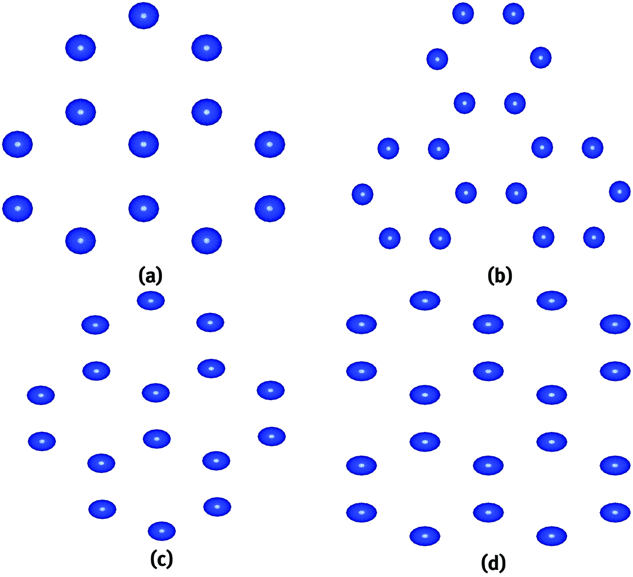
The schematic structures of four differently shaped nanodisks: (a) zigzag trigonal (ZT), (b) armchair trigonal (AT), (c) diamond shaped (DS) and (c) bowtie shaped (BS).
The magnetic and optical properties of differently shaped nanodisks have been first studied by Chowdhury et al. [67] by employing DFT. Four differently shaped nanodisks : zigzag trigonal (ZT), armchair triangular (AT), diamond shaped (DS) and bowtie shaped (BS) have been considered for the study. In Figure 2, we have schematically illustrated the structures of four differently shaped nanodisks. Edge atoms play a very important role in these kinds of nanodisks. Now, the percentage of the atoms at the edges of ZT, AT, DS and BS are, respectively, given by 69.2, 66.6, 62.6 and 60%. From the real part of the dielectric function data, an oscillatory behaviour up to 9 eV has been found for ZT and AT nanodisks. Beyond this energy range, the optical response becomes negligible. The static values of the real part of the dielectric function of all the nanodisks are found to be less than that of bulk Si and silicene. Different values of the dielectric function for different nanodisks can be traced due to anisotropy and different shape geometry. The comparison of optical properties of four different nanodisks shows that DS nanodisk has the best optical response, whereas AT bears the most poor optical response. This kind of study is very important for device fabrication in nano-optoelectronic technology and material characterization techniques.

(Top panel) Real (
Magnetic properties of single-vacancy (SV), DV, Al and P doped silicene have already been studied by Majumdar et al. [68]. In Figure 3, we have illustrated the real and imaginary parts of the dielectric function for SV and DV-induced silicene nanosheet as a function of energy for perpendicular polarization. From the figure, it can be observed that the signature of vacancy is mainly appeared within 6–10 eV. Also, the effect of both SV and DV is quite similar in the optical spectrum. Due to the presence of vacancy within the sample, the optical response is poor as can be seen from the magnitude of the dielectric functions. The maximum value of the imaginary part of the dielectric function is only 0.25. In the case of the real part, it varies between 0.85 and 1.15. Wei et al. [69] in 2013 and in 2016 Zakerian and Berahman [70] have studied the optical absorption of SV-induced silicene sheet by employing both DFT and Bethe Salpeter equation (BSE). As BSE takes into account the electron–hole interaction which DFT does not, so BSE employed data is expected to be more accurate than DFT. They have obtained two peaks in pristine silicene, one is located around 1.2 eV and the other one is around 4 eV [69]. SV-induced silicene has also shown two peaks like the pristine one, but here interestingly the two peaks are red-shifted. This happens due to the presence of dangling bond in the defected silicene. This characteristic feature can help the experimentalist to distinguish pristine silicene and defected silicene apart from Raman study.
DFT can only predict the ground-state properties of a many-body system as it is based on frozen atom approximation. But, if one can incorporate appropriate lattice dynamics and also choose thermally equilibrated configurations, then various optical properties can be computed at finite temperature which can be matched with the experiment. Now, to generate various thermally equilibrated configurations, molecular dynamics (MD) is a commonly adopted computational tool. From those configurations, one can compute the ensemble average of dielectric functions [71]. Yang and Liu [72] adopted this technique to calculate the dielectric function of monolayer silicene sheet. Apart from 0 K, they have considered two more temperatures 300 and 600 K. At each configuration, they have calculated the imaginary part of the dielectric function and then they have plotted the ensemble average of the imaginary part of the dielectric function. It has been revealed from their study that for parallel polarization, absorption peak around 1 eV energy range is enhanced consistently with increase of temperature. It has been explained through zero-energy gap and intraband transition which generally dominates the optical absorption occurring at low energy. With the increase of temperature, the amplitude of lattice vibrations is enhanced. As a result, more and more free carriers participate in the intraband transition which are thermally excited. But in the case of perpendicular polarization, due to structural disorder, the bands tend to spread out which reduce the absorption peaks. It will be interesting if these kinds of study can be done with silicene with defects.
Ye et al. [73] have studied the optical properties of periodically removed hexagonal silicon chains from silicene sheet, which is known as silicene nanomesh. While plotting the imaginary part of the dielectric function, they have observed a striking difference with that of bulk Si for both polarized and unpolarized light. Bulk Si has a threshold value of 1.1 eV below which there is no direct optical transitions occurring between the valence band maximum (VBM) and the conduction band minimum (CBM) [74]. It has been noticed that the maximum value of the imaginary part of the dielectric function lie within the visible to infrared (IR)\ part of the spectrum. The peak positions also do not noticeably change for the unpolarized and for parallely polarized light; however, the magnitude is doubled for parallely polarized light. But a strong anisotropy signal is noticed for both kinds of polarizations. The authors further commented that silicene nanomesh may pave the ways towards the fabrication of solar cell.
It is to be noted that quite a lot of theoretical works have already been done on the optical properties of silicene. But experimental works related to the exploration of optical properties are still inadequate. Sugiyama et al. [75, 76] have synthesized and also studied the optical properties of phenyl-modified (oxygen free) organosilicon nanosheet. The consequence reported of this structure is its uniform dispersion in organic solvents. The material has been synthesized by the reaction of layered polysilane [
![Figure 4: Comparison of absorbance spectra of graphene, silicene and germanene. Graphene: 0.02293, silicene: 0.02290, germanene: 0.02292. The universal behaviour is noticed for all of them, and this is independent of group IV elements, buckling and Fermi velocity (Reprinted with permission from Ref. [81]). Copyright (2012) by American Institute Physics.](/document/doi/10.1515/psr-2016-5102/asset/graphic/j_psr-2016-5102_fig_004.jpg)
Comparison of absorbance spectra of graphene, silicene and germanene. Graphene: 0.02293, silicene: 0.02290, germanene: 0.02292. The universal behaviour is noticed for all of them, and this is independent of group IV elements, buckling and Fermi velocity (Reprinted with permission from Ref. [81]). Copyright (2012) by American Institute Physics.
Before ending this section, we would like to mention one more remarkable feature of the optical properties of these 2D materials. After the immediate discovery of graphene, it has been realized that the transmittance can be defined in terms of fine structure constant (
Magnetic properties of doped FS silicene monolayer
Pristine FS monolayer silicene is non-magnetic like that of graphene [84]. But, the presence of defects like vacancy or adatoms can make silicene magnetic. This kind of metal free magnetism is now the subject of an intense research. This type of magnetism comes due to the formation of localized states caused by defects or molecular adsorption. Inducing magnetism into non-magnetic nanostructure is technologically very important for making quantum information and spintronic devices. Below, we will review some of the recent work based on magnetic properties of monolayer FS silicene sheet.
The phenomenon of ferromagnetism observed at reasonably high temperatures in some compounds which do not contain any atoms with open
![Figure 5: The total magnetic moments of the spin-polarized systems as a function of adsorption concentration (Reprinted with permission from Ref. [97]). Copyright (2016) by Elsevier.](/document/doi/10.1515/psr-2016-5102/asset/graphic/j_psr-2016-5102_fig_005.jpg)
The total magnetic moments of the spin-polarized systems as a function of adsorption concentration (Reprinted with permission from Ref. [97]). Copyright (2016) by Elsevier.
Hydrogenation and halogenation is one of the viable route to induce magnetism in silicene. Zheng et al. [98] have employed the first-principle calculation to investigate the magnetic properties of silicene sheet adsorbed with H and Br atoms. It has been found that when the silicene sheet is fully saturated with H and Br atoms, the ground state is found to be non-magnetic. But when the sheet is half-saturated from one side, it shows ferromagnetic property. It is due to localized and unpaired electrons of the unsaturated Si atoms. Total energy calculation reveals that half-hydrogenated silicene exhibits ferromagnetic order [99], while half-brominated one exhibits antiferromagnetic ordering. Paszkowska and Krawiec [100] have explored the stability of magnetism in hydrogenated silicene under the influence of strain, charge doping and external electric field. It has been found that the magnetism is present in strained hydrogenated silicene unless a structural phase transition occurs. As long as the hydrogenated silicene maintains its LB structure, strain does not influence the magnetic property of the system. However, when an external electric field is applied, then it has been observed that the magnetic ground state is still maintained. But interestingly, the magnetism disappeared for both electron and hole doping. Zhang et al. [101] have investigated the magnetic properties of different hydrogenated conformer of silicene sheets. It has been noticed that half-hydrogenated chair-like conformer shows magnetic ground state. This is because of the
Inducing magnetism in a non-magnetic material by transition metal (TM) atoms [104] is a conventional process due to their half filled
Table for magnetic moment (in
| Atoms | Magnetic moment ( | Reference |
| Cr (A) | 4.01/cell | [105] |
| Mn (A) | 5.08/cell | [105] |
| Fe (A) | 2.21/cell | [105] |
| Co (A) | 0.0/cell | [105] |
| Cr (D) (unstrained) | 2.0 | [106] |
| Cr (D) (strain | 4.0 | [106] |
| Fe (D) (unstrained) | 0.4 | [106] |
| Fe (D) (strain | 4.0 | [106] |
| Ti (D) | 2.0 | [107] |
| V (D) | 2.27 | [107] |
| Cr (D) | 4.0 | [107] |
| Mn (D) | 3.0 | [107] |
| Fe (D) | 2.0 | [107] |
| Co (D) | 1.0 | [107] |
| Si (A) | 2.0 | [108] |
| H (A) | 1.0 | [108] |
| Ti (A) | 2.0 | [108] |

Magnetic moment (in
Vacancy-induced magnetism has also been one of the interesting topic in condensed matter and material physics. Here also the absence of
![Figure 7: Magnetic moments of silicene with embedded TM atoms in SV (red) and DV (black) defects (Reprinted with permission from Sun et al. [110]. Copyright @ American Institute of Physics (2015)).](/document/doi/10.1515/psr-2016-5102/asset/graphic/j_psr-2016-5102_fig_007.jpg)
Magnetic moments of silicene with embedded TM atoms in SV (red) and DV (black) defects (Reprinted with permission from Sun et al. [110]. Copyright @ American Institute of Physics (2015)).
![Figure 8: Bar diagram of magnetic moments of TM atoms embedded into N or C doped SV defect in silicene. The green bars indicate the magnetic moments of transition metal atoms embedded into SV without doping for comparison. The inset shows the configurations of TM atoms in C-doped SV (Reprinted with permission from Sun et al. [110]. Copyright @ American Institute of Physics (2015)).](/document/doi/10.1515/psr-2016-5102/asset/graphic/j_psr-2016-5102_fig_008.jpg)
Bar diagram of magnetic moments of TM atoms embedded into N or C doped SV defect in silicene. The green bars indicate the magnetic moments of transition metal atoms embedded into SV without doping for comparison. The inset shows the configurations of TM atoms in C-doped SV (Reprinted with permission from Sun et al. [110]. Copyright @ American Institute of Physics (2015)).
The use of superhalogen (
![Figure 9: Top view of the schematic representation of adatom adsorbed silicene on different adsorption sites: (i) on hollow site (HS), (ii) on bridge site (BS) and (iii) on top site (TS) (Reprinted with permission from Nath et al. [53]. Copyright @ Elsevier (2015)).](/document/doi/10.1515/psr-2016-5102/asset/graphic/j_psr-2016-5102_fig_009.jpg)
Top view of the schematic representation of adatom adsorbed silicene on different adsorption sites: (i) on hollow site (HS), (ii) on bridge site (BS) and (iii) on top site (TS) (Reprinted with permission from Nath et al. [53]. Copyright @ Elsevier (2015)).
The optical properties of four differently shaped silicene nanodisks [67] have been described in the previous section. It has been found that among the four nanodisks, only ZT silicene nanodisk is magnetic in nature having
Elemental structure and synthesis of FS germanene
Germanene follows the hexagonal honeycomb-like atomic arrangement of graphene with two atoms per unit cell. As mentioned earlier, SOC plays an important role in various properties of these 2D materials. Germanene possesses a very high value of SOC (
Germanene has been synthesized by Davila et al. [126], for the first time, through molecular beam epitaxy (MBE) using a gold (111) surface as substrate [126]. In the same year, almost in parallel, another group, Li et al., have successfully fabricated graphene-like germanene sheet on a Pt(111) surface. They have demonstrated clearly that the germanene grown on this surface was a 2D continuous layer with a buckled configuration [127]. Moreover, in order to synthesize germanene using a particular substrate, it is essential to gain sufficient knowledge about interaction of FS germanene with that substrate. Liu et al. in a work [128] have investigated about the interaction between oxygen (
Electronic and magnetic properties of FS germanene
Germanene exhibits similar electronic band structure like graphene with linear band dispersion relation and zero bandgap near Dirac K points if effect of SOC is not taken into account [118, 130, 131].
However, the inclusion of SOC introduces a non-zero value of bandgap at Dirac K point along with Dirac cone-like signatures, which again ensures about more fascinating properties and hence effective applications of germanene in optoelectronics, photo-voltaics, etc. Liu et al. have predicted [27] through a systematic first-principles investigations that an appreciable gap of 4 meV and 23.9 meV can be opened at Dirac points for planar and LB germanium, respectively, by SOC. These features are clearly depicted in Figure 10(a) and (b).

Relativistic band structure of germanium with honeycomb structure. (Left panel) the relativistic band structure of germanium with planar and (right panel) low-buckled honeycomb structure. Inset: Gap induced by SOC at Dirac K point (zooming).
Large amount of SOC indicates that germanene can exhibit QSHE in an experimentally accessible temperature regime, even at near room temperature [132]. Zhang et al. have studied the electronic properties of germanene sheets that are found on
Hydrogenated silicene and germanene, termed as silicane and germanane respectively, also possess very interesting electronic properties. M. Houssa et al. [139] have predicted that in both silicane and germanane, there is a finite band opening in the band structure. The type of gap in silicane is direct or indirect depending on its atomic configuration (chairlike or boatlike). But in the case of germanene, there is always a direct bandgap opening of about 3.2 eV independent of atomic configuration which makes this material potentially interesting for application in optoelectronic devices (shown in Figure 11(a), (b), (c) and (d)).

Band structures, calculated using LDA functional, (a) chairlike silicane, (b) boatlike silicane, (c) chairlike germanane and (d) boatlike germanane. Reference zero-energy level is set to the top of the valence band.
Rupp et al. [140] have reported about modifications in stability and electronic properties of germanene in the presence of impurity atoms using DFT. They have observed that the adsorption of one hydrogen (H) atom by boron (B) or nitrogen (N) impurities leads to p- and n-type semiconducting properties, respectively. Germanene, like all other 2D honeycomb structures of III–V binary compounds, is non-magnetic in nature [141]. Electronic and magnetic properties of germanene can be tuned by doping or adsorption of foreign elements in pristine system [141] or introducing vacancy or applying some strain engineering. Li et al. have proposed [142] an efficient technique of band opening by nanopatterning germanene into super-lattices using DFT. They have indicated that the broken sublattice symmetry in nanopattterning germanene is the reason for opening of bandgap. Recently, Liang et al. have explored [143] about the fact that surface functionalization and strain will modify electronic and magnetic properties of hydrogenated, fluorinated and chlorinated germanene by employing DFT. They have highlighted that fluorinated germanenes are energetically more stable than hydrogenated and chlorinated germanenes because fluorine atoms possess stronger electronegativity. Pang et al. [144] have studied the effect of alkali metal (AM) atoms adsorbed in germanene and indicated that it is possible to tailor both the gap and the concentration of charge carries of AM/germanene systems by controlling the coverage of AM. From their analysis, it is also evident that AM/germanene could be of great interest in nanoindustry, like FET applications due to strong binding of AM atoms with germanene and exceptional interesting properties of AM/germanene systems. In another work, Pang et al. have analysed [145] about the structural, electronic and magnetic properties of 3d-TM adsorbed germanene. It was concluded that in most TM/germanene structures TM–Ge bonds exhibit mostly covalent chemical bonding character. Electronic and thermal properties of germanene has been studied recently by Zaveh et al. [146] employing DFT and density functional perturbation theory (DFPT). They have observed that specific heat at constant volume (

Structures (a) pristine, (b) S1, (c) S2, (d) S3, (e) S4, (f) S5, (g) S6, (h) S7, (i) S8. Largest and light-green coloured atoms are Ga, medium and black coloured atoms are Ge, smallest and deep-yellow coloured atoms are As.
It is predicted from DFT calculations that semi-metallic germanene is transformed to metallic nature by incorporating single or double doping of As and Ga, whereas semi-metallic property is preserved for AsGa codoped configurations, which can be justified by observing the position of Fermi level (
Optical properties of FS germanene
Now, before going for the analysis of optical properties of germanene, we would like to review the optical properties of bulk Ge briefly. Values of static dielectric constant

Imaginary part of dielectric constant for FS 2D materials silicene (black-dashed) and germanene (red-dotted) calculated using DFT.
Optical properties of FS germanene can also be modified by incorporating doping of foreign elements significantly. It has been elucidated that the value of universal IR absorbance can be enhanced or reduced than pristine germanene by incorporating suitable combinations of doping elements, site of doping and concentration of doping [152]. Different optical properties in terms of the real part of dielectric constant have been investigated (

Real part of dielectric constant for perpendicular polarization. (a) As doped structures, (b) Ga doped structures, (c) AsGa codoped structures.
To analyse the optical properties, the electric field is applied for perpendicular polarization, that is along the axis (Z axis) perpendicular to the plane of germanene sheet. Value of
Structural properties of TG sheet
In their study [39], Enyashin et al. have used the DFT-based tight-binding method (DFTB) to successfully accomplish the optimizations of all the 12 structures by minimizing the total energy and forces between atoms up to reasonable satisfactory accuracy. Among those configurations, a structure with equal number of squares and octagons was previously studied by Zhu et al. [158]. The calculation [158] demonstrated that this structure with tetragonal symmetry retains its planar form even after geometrical relaxation. The relaxed network consists of a single type of
Electronic properties of pristine and functionalized TG sheet
The electronic properties of planar TG was first reported by Enyashin et al. [39]. Their calculated band structure has revealed that
TG nanoribbons (NRs) and clusters
Along with two types of TG sheets, Liu et al. [159] also investigated the variation of their properties with structural modifications, i.e. confinements. For buckled TG, armchair-like ribbon with width of one lattice constant (square-octagon periodic repetition along one direction) has the strongest quantum confinement and explores the linear dispersion relation. Whereas, periodic repetition of octagons, i.e. zigzag-like TGNR, exhibits metallic properties. Furthermore, spin-polarized first-principles calculations by them have indicated that zigzag-like TGNR prefers ferromagnetic state, while the former one is diamagnetic. Motivated by these intriguing properties of square-octagon repeated nets, Wang et al. [167] have employed first-principles study to investigate the structural and electronic properties of another tetra-symmetrical planar structure with space group P4/mmm. Lattice constant of the structure is 3.447 Å and its unit cell consists of 4 C atoms. Proper relaxation shows that, unlike graphene and the TG proposed by Liu et al., it consists of two distinct bonds (with bond lengths of 1.372 Å and 1.467 Å) and two different angles (
Later, Dai et al. [168] have investigated the transport properties of the TGNRs. In that work, they have also supported the width-dependent metal–semiconductor oscillations by calculating a general expression for the bandgap.
For further details about these tetrasymmetrical structures, first-principles based Raman and IR spectra have been investigated for different cluster sizes [169]. The study has revealed that a phonon Raman mode appearing near 1,711–1,713 cm
Other allotropes beyond TG
Apart from the above-mentioned TG allotrope, there are other competitors with overwhelming properties. Some of them are briefly discussed in this section.
Partial replacement of
Graphdiyne [176], first designed by Haley et al. [177], is composed of two acetylenic linkages between nearest-neighbour hexagonal rings and belongs to the space group P6mm. Later, many interesting properties like high degree of stability against temperature, semiconducting behaviour with silicon-like conductivity [178] and applicability in nanoscale devices [179] were reported. Interestingly, graphdiyne nanoribbons and nanotubes are experimentally synthesized and found to be useful in optoelectronic and spintronics [179, 180].
Another proposed allotrope is penta-graphene [181] which is composed of pentagons with C at its vertices, which closely resembles MacMohon’s net, a semiregular tiling of the Euclidean plane similar to Cairo pentagonal tiling. Total thickness of this 2D multidecker sandwich sheet is found to be 1.2 Å. The structure possesses
Stone–Wales (SW) defects are formed by a
Another 2D allotropes can be achieved by systematic tessellations of octagons and pentagons (OP). Such alignments are of two types as predicted by Su et al. [185]. This can be viewed as colligating of ribbons formed by five-five-eight membered rings along a straight line path (for OPG-L) or along a zigzag path (OPG-Z). These structures are energetically more favourable than recently synthesized graphdiyne. Further studies on electronic properties indicate that OPG-L is a metal while OPG-Z is a gapless semi-metal.
Replacement of one-third
Some other possible allotropes are also drawing keen attention of the researchers because of their novel exotic properties as follows. S-graphene is a periodic arrangement of six- and four-member rings with eight atoms in its unit cell. Similarly, D-graphene and E-graphenes are composed of
Although mostly electronic and structural properties in these materials are explored, however, studies involving the optical properties including Raman are still lacking. We hope to get a good direction if some of these materials are synthesized.

Favourable site for Li adsorption on planar TG. The arrows denote Li diffusion paths from the octagonal site to a neighbouring one.

Raman and IR spectra of
Conclusions and future directions
In this chapter, we have attempted to cover some important contributions of the electronic, magnetic and optical properties (including Raman spectroscopy) of silicene, germanene and T-graphene.

IR spectra of pristine and doped 3×3 TG clusters.

All graphene allotropes except TG (a) α graphyne, (b) β graphyne, (c) γ graphyne, (d) graphdiyne, (e) penta-graphene, (f) pentaheptites (g) R-graphene.
Silicene, one of the graphene’s cousins, does not exist in nature in FS form; however, they can be synthesized on suitable metal single-crystal substrates. Tunability of the material properties in such elemental silicene sheets and disks (edge related) or nanoribbons offers a novel prospect of engineering discrete applications. Theoretical DFTB calculations have shown to indicate an appropriate direction to these silicene derivatives. Most of the silicene derivatives have been grown on metallic substrates; however, for device fabrication, these metallic substrates are not appropriate. It will be interesting to grow the various forms (single layer or multilayer) of silicene and its important derivatives on non-metallic or insulating substrates at a large scale. This will also aid to control the effective van der Waals interaction existing between the layers and the in-place lattice separation to modify effectively the band structure of Dirac fermions, if any, present in the structure. It is important to note that existing Si-based technologies recently is facing intrinsic limits with top-down approaches. It is therefore highly desirable that further experimental investigations should be pursued in order to exploit these theoretical predictions. These aspects can open in future a new horizon for low-dimensional, competitive and durable storage technologies.
Next to graphene and silicene, germanene stands as a fascinating material which can definitely be used in 2D nanoindustry in near future due to its unique and outstanding properties than graphene or silicene. Higher values of SOC and buckling designate germanene as a more efficient material for practical applications than graphene or silicene. Though it is not possible to fabricate FS germanene till date, germanene layers grown by using substrate material possess electronic and optical properties which can easily be compared with FS structure. Higher carrier mobility of germanene than graphene or silicene also manifest its practical applications. It is also possible to modify the properties of pristine germanene by means of different mechanisms which is one of the most current research interest. We firmly suggest that there are many unconventional properties of germanene which are still unexplored. This offers researchers a new way for investigation, theoretical as well as experimental, about germanene in nanoelectronics.
Although some preliminary studies both in theory and in synthesis processes are done, however, it is necessary to explore some modifications of their electronic band structure and optical properties in the presence of combinations of strains, doping and defects. Armed with theoretical predictions from DFT/TB, we strongly feel that there are unexpected properties of various structures made from silicene and germanene.
It is shown that structural modifications by changing the symmetry and tailoring the structure may influence the structural and electronic properties. For graphene allotropes, a class of materials show metallic behaviour, some of them are semiconducting and rest are semi-metals. This wide variety of bandgaps along with their appreciable structural stability directed towards the usefulness of these material in device formations. Among all the graphene allotropes, tetrasymmetrical graphene is dynamically more stable than graphyne and the recently prepared graphdiyne and has appreciable DOS at EF. The bandgap of this material can be tuned by varying the ribbon width. In addition, TG sheet can be used as a gas storage media. Apart from these informations, other properties of these structures are relatively less explored. Hopefully, all the intriguing properties of TG and other graphene allotropes can be verified in real life by forming different optoelectronic devices, with the support of recent experimental progresses.
The unique intriguing features associated with these novel 2D structures beyond graphene are expected to overcome fundamental constraints imposed on dimensional physical limits on the evolution of faster, smaller and smart nanoelectronics devices in the near future.
Funding statement: This work is partially supported by DST-FIST, DST-PURSE, Government of India. Two of the authors (SC) and (ND) gratefully acknowledge DST, Government of India, for providing financial assistance through DST-INSPIRE Fellowship scheme of grant number IF120579 and IF150670.
Correction Statement
Correction added after ahead-of-print publication on 16 May 2017: The DOI of this article has been corrected to: https://doi.org/10.1515/psr-2016-5102.
The DOI of this article has been used for another publication by mistake. If you intended to access the other publication, please use this link: https://doi.org/10.1515/psr-2016-0102
Acknowledgement
This article is also available in: Ramasami, Computational Sciences. De Gruyter (2017), isbn 978–3–11–046536–5.
References
1. Novoselov KS, Mishchenko A, Carvalho A, Castro Neto AH. 2D materials and van der Waals heterostructures. Science. 2016;353:461–472.10.1126/science.aac9439Search in Google Scholar PubMed
2. Novoselov KS, Geim AK, Morozov SV, Jiang D, Zhang Y, Dubonos SV, et al. Electric field effect in atomically thin carbon films. Science. 2004;306:666–669 .10.1126/science.1102896Search in Google Scholar PubMed
3. Novoselov KS, Geim AK, Morozov SV, et al. Two-dimensional gas of massless Dirac fermions in graphene. Nature. 2005;438:197–200.10.1038/nature04233Search in Google Scholar PubMed
4. Geim AK, Grigorieva I. Van der Waals heterostructures. Nature. 2013;499:419–425.10.1038/nature12385Search in Google Scholar PubMed
5. Gupta A, Sakthivel I, Seal S. Recent development in 2D materials beyond graphene. Prog Mater Sci. 2015;73:44–126.10.1016/j.pmatsci.2015.02.002Search in Google Scholar
6. Jana D, Sun CL, Chen LC, Chen KH. Effect of chemical doping of boron and nitrogen on the electronic, optical, and electrochemical properties of carbon nanotubes. Prog Mater Sci. 2013;58:565–635.10.1016/j.pmatsci.2013.01.003Search in Google Scholar
7. Balendhran S, Walia S, Nili H, Sriram S, Bhaskaran M. Elemental analogues of graphene: silicene, germanene, stanene, and phosphorene. Small. 2014;11:640–652.10.1002/smll.201402041Search in Google Scholar PubMed
8. Kara A, Enriquez H, Seitsonen AP. A review on silicene-new candidate for electronics. Surf Sci Rep. 2012;67:1–18.10.1016/j.surfrep.2011.10.001Search in Google Scholar
9. Lew Yan, Voon LC, Guzmán-Verri GG. Is silicene the next graphene? MRS Bull., 2014;39:366–373.Search in Google Scholar
10. Xu M, Liang T, Shi M, Chen H. Graphene-like two-dimensional materials. Chem Rev. 2013;113:3766–3798.10.1021/cr300263aSearch in Google Scholar PubMed
11. Yamada-Takamura Y, Friedlein R. Progress in the materials science of silicene. Sci Technol Adv Mater. 2014;15 064404 (12pp).10.1088/1468-6996/15/6/064404Search in Google Scholar PubMed PubMed Central
12. Vogt P, Padova PD, Quaresima C, et al. Silicene: compelling experimental evidence for graphenelike two-dimensional silicon. Phys Rev Lett. 2012;108:155501–155504.10.1103/PhysRevLett.108.155501Search in Google Scholar PubMed
13. Cinquanta E, Scalise E, Chiappe D, et al. Getting through the nature of silicene: an sp2–sp3 two-dimensional silicon nanosheet. J Phys Chem C. 2013;117:16719–16724.10.1021/jp405642gSearch in Google Scholar
14. Lin CL, Arafune R, Kawahara K, et al. Structure of silicene grown on Ag(111). Appl Phys Exp. 2012;5 045802(3pp).10.1143/APEX.5.045802Search in Google Scholar
15. Feng B, Ding Z, Meng S, et al. Evidence of silicene in honeycomb structures of silicon on Ag(111). Nano Lett. 2012;12:3507–3511.10.1021/nl301047gSearch in Google Scholar PubMed
16. Chen L, Li H, Feng B, et al. Spontaneous symmetry breaking and dynamic phase transition in monolayer silicene. Phys Rev Lett. 2013;110 085504(5pp).10.1103/PhysRevLett.110.085504Search in Google Scholar PubMed
17. Meng L, Wang Y, Zhang L, et al. Buckled silicene formation on Ir(111). Nano Lett. 2013;13:685–690.10.1021/nl304347wSearch in Google Scholar PubMed
18. Fleurence A, Friedlein R, Ozaki T, Kawai H, Wang Y, Yamada-Takamura Y. Experimental evidence for epitaxial silicene on diboride thin films. Phys Rev Lett. 2012;108:245501–245504.10.1103/PhysRevLett.108.245501Search in Google Scholar PubMed
19. Roome NJ, Carey JD. Beyond graphene: stable elemental monolayers of silicene and germanene. ACS Appl Mater Interfaces. 2014;6:7743–7750.10.1021/am501022xSearch in Google Scholar PubMed
20. Chowdhury S, Jana D. A Theoretical review on electronic, magnetic and optical properties of silicene. Rep Prog Phys. 2016;79 126501 (57pp).10.1088/0034-4885/79/12/126501Search in Google Scholar PubMed
21. Zhuang J, Xu X, Feng H, Li Z, Wang X, Du Y. Honeycomb silicon: a review of silicene. Sci Bull. 2015;60:1551–1562.10.1007/s11434-015-0880-2Search in Google Scholar
22. Oughaddou H, Enriquez H, Tchalala MR, et al. Silicene, a promising new 2D material. Prog Surf Sci. 2015;90:46–83.10.1016/j.progsurf.2014.12.003Search in Google Scholar
23. Ni Z, Liu Q, Tang K, et al. Tunable bandgap in silicene and germanene. Nano Lett. 2012;12:113–118.10.1021/nl203065eSearch in Google Scholar PubMed
24. Drummond ND, Zólyomi V, Fal’ko VI. Electrically tunable band gap in silicene. Phys Rev B. 2012;85:075423–075427.10.1103/PhysRevB.85.075423Search in Google Scholar
25. Mohan B, Kumar A, Ahluwalia PK. Electronic, mechanical and dielectric properties of silicane under tensile strain. Phys E. 2013;53:233–239.10.1016/j.physe.2013.05.014Search in Google Scholar
26. Liu CC, Jiang H, Yao YG. Low-energy effective Hamiltonian involving spin-orbit coupling in silicene and two-dimensional germanium and tin. Phys Rev B. 2011;84:195430–195440.10.1103/PhysRevB.84.195430Search in Google Scholar
27. Liu CC, Feng W, Yao YG. Quantum spin hall effect in silicene and two-dimensional germanium. Phys Rev Lett. 2011;107 076802 (4pp).10.1103/PhysRevLett.107.076802Search in Google Scholar PubMed
28. Qi XL, Zhang SC. Topological insulators and superconductors. Rev Mod Phys. 2011;83:1057–1110.10.1103/RevModPhys.83.1057Search in Google Scholar
29. Garcia JC, de Lima DB, Assali LVC, Justo JF. Group IV graphene- and graphane-like nanosheets. J Phys Chem C. 2011;115:13242–13246.10.1021/jp203657wSearch in Google Scholar
30. Durgun E, Tongay S, Ciraci S. Silicon and III-V compound nanotubes: structural and electronic properties. Phys Rev B2005;72:075420 zcelik VO, Ciraci S. Self-assembly mechanisms of short atomic chains on single-layer graphene and boron nitride. Phys Rev B 2012;86:155421. Ataca C, Ciraci S. Functionalization of single-layer MoS2 honeycomb structures. J Phys Chem C2011;115:1330.Search in Google Scholar
31. Houssa M, van den Broek B, Scalise E, et al. Theoretical aspects of graphene-like group IV semiconductors. Appl Surf Sci. 2014;291:98–103.10.1016/j.apsusc.2013.09.062Search in Google Scholar
32. Qui J, Fu H, Xu Y, et al. From Silicene to Half-Silicane by Hydrogenation. ACS Nano. 2015;9:11192–11199.10.1021/acsnano.5b04722Search in Google Scholar PubMed
33. Wang W, Olovsson W, Uhrberg RIG. Band structure of hydrogenated silicene on Ag(111): evidence for half-silicane. Phys Rev B. 2016;93 081406(R)(4pp).10.1103/PhysRevB.93.081406Search in Google Scholar
34. Tao L, Cinquanta E, Chiappe D, et al. Silicene field-effect transistors operating at room temperature. Nature Nanotechnol. 2015;10:227–231.10.1038/nnano.2014.325Search in Google Scholar
35. Tang Q, Zhou Z. Graphene-analogous low-dimensional materials. Prog Mater Sci. 2013;58:1244–1315.10.1016/j.pmatsci.2013.04.003Search in Google Scholar
36. Liu H, Gao J, Zhao J. Silicene on substrates: a way to preserve or tune its electronic properties. J Phys Chem C. 2013;117:10353–10359.10.1021/jp311836mSearch in Google Scholar
37. Kaloni TP, Schreckenbach G, Freund MS, Schwingenschlogl U. Current developments in silicene and germanene. Phys Status Solidi RRL. 2016;10:133–142.10.1002/pssr.201510338Search in Google Scholar
38. Butler SZ, Hollen SM, Cao L, et al. Progress, challenges, and opportunities in two-dimensional materials beyond graphene. ACS Nano. 2013;7:2898–2926.10.1021/nn400280cSearch in Google Scholar
39. Enyashin AN, Ivanovskii AL. Graphene allotropes. Phys Status Solidi B. 2011;248:1879–1883.10.1002/pssb.201046583Search in Google Scholar
40. Heimann RB, Evsyukov SE, Koga Y. Carbon allotropes: a suggested classification scheme based on valence orbital hybridization. Carbon. 1997;35:1654–1658.10.1016/S0008-6223(97)82794-7Search in Google Scholar
41. Mas-Balleste R, Gomez-Navarro C, Gomez-Herrero J, Zamora F. 2D materials: to graphene and beyond. Nanoscale. 2011;3:20–30.10.1039/C0NR00323ASearch in Google Scholar
42. Hohenberg P, Kohn W. Inhomogeneous electron gas. Phys Rev. 1964;136:B864–871.10.1103/PhysRev.136.B864Search in Google Scholar
43. Kohn W, Sham LJ. Self-consistent equations including exchange and correlation effects. Phys Rev. 1965;140:A1133–1138.10.1103/PhysRev.140.A1133Search in Google Scholar
44. Kohn W. Nobel lecture: electronic structure of matter–wave functions and density functionals. Rev Mod Phys. 1999;71:1253–1266.10.1103/RevModPhys.71.1253Search in Google Scholar
45. Guistino F. Materials modelling using density functional theory. Oxford: Oxford University Press, 2014.Search in Google Scholar
46. Nath P, Chowdhury S, Sanyal D, Jana D. Ab-initio calculation of electronic and optical properties of nitrogen and boron doped graphene nanosheet. Carbon. 2014;73:275–282.10.1016/j.carbon.2014.02.064Search in Google Scholar
47. Eberlein T, Bangert U, Nair RR, et al. Plasmon spectroscopy of free-standing graphene films. Phys Rev B. 2008;77 233406(4pp).10.1103/PhysRevB.77.233406Search in Google Scholar
48. Heyd J, Scuseria GE, Ernzerhof M. Hybrid functionals based on a screened Coulomb potential. J Chem Phys 2003;1188207 (9pp). Erratum : J Chem Phys. 2006;124(219906):1.10.1063/1.1564060Search in Google Scholar
49. Perdue JP, Burke K, Ernzerhof M. Generalized gradient approximation made simple. J Chem Phys. 1996;105 9982 (4 pp).10.1103/PhysRevLett.77.3865Search in Google Scholar PubMed
50. Mahan GD. Many particle physics. New York, NY: Plenum Press, 1990.10.1007/978-1-4613-1469-1Search in Google Scholar
51. Dressel M, Gruner G. Electrodynamics of solids. Cambridge: Cambridge University Press, 2002.10.1017/CBO9780511606168Search in Google Scholar
52. Nath P, Sanyal D, Jana D. Ab-initio calculation of optical properties of AA-stacked bilayer graphene with tunable layer separation. Curr Appl Phys. 2015;15:691–697.10.1016/j.cap.2015.03.011Search in Google Scholar
53. Nath P, Sanyal D, Jana D. Optical properties of transition metal atom adsorbed graphene: a density functional theoretical calculation. Phys E. 2015;69:306–315.10.1016/j.physe.2015.02.004Search in Google Scholar
54. Das R, Chowdhury S, Jana D. A first principles approach to magnetic and optical properties in single-layer graphene sandwiched between boron nitride monolayers. Mater Res Express. 2015;2 075601(12pp).10.1088/2053-1591/2/7/075601Search in Google Scholar
55. Chowdhury S, Das R, Nath P, Jana D, Sanyal D. Electronic and optical properties of boron- and nitrogen-functionalized graphene nanosheet. In: Thakur VK, Thakur MK, editors. Chemical functionalization of carbon nanomaterials : chemistry and applications. New York, NY: CRC Press Chapter 42, 2015:949–957.Search in Google Scholar
56. Yu PY, Cardona M. Fundamentals of semiconductors physics and materials properties. New York, NY: Springer, 2010.10.1007/978-3-642-00710-1Search in Google Scholar
57. Kamal C, Banerjee A, Chakrabarti A. In: Aliofkhazraei M, editors. Properties of two-dimensional silicon versus carbon systems graphene science handbook size-dependent properties.. New York, NY: CRC Press. Chapter 15 221–234pp ISBN 9781466591356 – CAT# K20509 2016.Search in Google Scholar
58. Bao H, Guo J, Liao W, Zhao H. Electrical engineering of the optical properties in silicene. Appl Phys A. 2015;118:431–5.10.1007/s00339-014-8837-xSearch in Google Scholar
59. Hu W, Li Z, Structural Yang J. electronic, and optical properties of hybrid silicene and graphene nanocomposite. J Chem Phys. 2013;139 154704 (5pp).10.1063/1.4824887Search in Google Scholar PubMed
60. Mohan B, Kumar A, Ahluwalia PK. Electronic and optical properties of silicene under uni-axial and bi-axial mechanical strains: a first principle study. Phys E. 2014;61:40–47.10.1016/j.physe.2014.03.013Search in Google Scholar
61. Matthes L, Gori P, Pulci O, Bechstedt F. Universal infrared absorbance of two-dimensional honeycomb group-IV crystals. Phys Rev B. 2013;87 035438(9pp).10.1103/PhysRevB.87.035438Search in Google Scholar
62. Matthes L, Pulci O, Bechstedt F. Optical properties of two-dimensional honeycomb crystals graphene, silicene, germanene, and tinene from first principles. New J Phys. 2014;16 105007(13pp).10.1088/1367-2630/16/10/105007Search in Google Scholar
63. Das R, Chowdhury S, Majumdar A, Jana D. Optical properties of P and Al doped silicene: a first principles study. RSC Adv. 2014;5:41–50.10.1039/C4RA07976KSearch in Google Scholar
64. Ezawa M. Peculiar band gap structure of graphene nanoribbons. Phys Stat Sol C. 2007;4:489–492.Search in Google Scholar
65. Rader HJ, Rouhanipour A, Talarico AM, Palermo V, Samor P, Mullen K. Processing of giant graphene molecules by soft-landing mass spectrometry. Nat Mater. 2006;5:276–280.10.1038/nmat1597Search in Google Scholar PubMed
66. Sony P, Shukla A. A general purpose Fortran 90 electronic structure program for conjugated systems using Pariser-Parr-Pople model. Comput Phys Commun. 2010;181:821–830.10.1016/j.cpc.2009.12.015Search in Google Scholar
67. Chowdhury S, Nath P, Jana D. Shape dependent magnetic and optical properties in silicene nanodisks: a first principles study. J Phys Chem Sol. 2015;83:32–39.10.1016/j.jpcs.2015.03.017Search in Google Scholar
68. Majumdar A, Chowdhury S, Nath P, Jana D. Defect induced magnetism in planar silicene: a first principles study. RSC Adv. 2014;4:32221–32227.10.1039/C4RA04174GSearch in Google Scholar
69. Wei W, Dai Y, Huang B, Jacob T. Many-body effects in silicene, silicane, germanene and germanane. Phys Chem Chem Phys. 2013;15 8789(6pp).10.1039/c3cp51078fSearch in Google Scholar PubMed
70. Zakerian F, Berahman M. Optical properties of defected silicene: the many-body approach. Opt Quant Electron. 2016;48 370 (7pp).10.1007/s11082-016-0637-4Search in Google Scholar
71. Ekardt W. Metal clusters. New York, NY: John Wiley and Sons Ltd., 1999.Search in Google Scholar
72. Yang JY, Liu LH. Temperature-dependent dielectric functions in atomically thin graphene, silicene, and arsenene. Appl Phys Lett. 2015;107 091902(4pp).10.1063/1.4930025Search in Google Scholar
73. Ye XS, Shao ZG, Zhao H, Yang L, Wang CL. Electronic and optical properties of silicene nanomeshes. RSC Adv. 2014;4:37998–38003.10.1039/C4RA03942DSearch in Google Scholar
74. Guo L, Zhang S, Feng W, Hu G, Li W. A first-principles study on the structural, elastic, electronic, optical, lattice dynamical, and thermodynamic properties of zinc-blende CdX (X = S, Se, and Te). J Alloys Compd. 2013;579:583–593.10.1016/j.jallcom.2013.07.096Search in Google Scholar
75. Sugiyama Y, Okamoto H, Mitsuoka T, et al. Synthesis and optical properties of monolayer organosilicon nanosheets. J Am Chem Soc. 2010;132:5946–5947.10.1021/ja100919dSearch in Google Scholar PubMed
76. Wang R, Xu M, Pi X. Chemical modification of silicene. Chin Phys B. 2015;24 086807 (21pp).10.1088/1674-1056/24/8/086807Search in Google Scholar
77. Okamoto H, Nakano H, Sugiyama Y. Synthesis and modification of silicon nanosheets and other silicon nanomaterials. Chem Eur J. 2011;17:9864–9887.10.1002/chem.201100641Search in Google Scholar PubMed
78. Nakano H, Nakano M, Nakanishi K, et al. Preparation of alkyl-modified silicon nanosheets by hydrosilylation of layered polysilane ($Si_6H_6$Si6H6). J Am Chem Soc. 2012;134:5452–5455.10.1021/ja212086nSearch in Google Scholar PubMed
79. Borensztein Y, Prevot G, Masson L. Large differences in the optical properties of a single layer of Si on Ag(110) compared to silicene. Phys Rev B. 2014;89 245410 (7pp).10.1103/PhysRevB.89.245410Search in Google Scholar
80. Matthes L, Pulci O, Bechstedt F. Massive dirac quasiparticles in the optical absorbance of graphene, silicene, germanene, and tinene. J Phys Condens Matter. 2013;25 395305(7pp).10.1088/0953-8984/25/39/395305Search in Google Scholar PubMed
81. Bechstedt F, Matthes L, Gori P, Pulci O. Infrared absorbance of silicene and germanene. Appl Phys Lett. 2012;100 261906(4pp).10.1063/1.4731626Search in Google Scholar
82. Nair RR, Blake P, Griaorenko AN, et al. Fine structure constant defines visual transparency of graphene. Science. 2008;320 1308(9pp).10.1126/science.1156965Search in Google Scholar PubMed
83. Pulci O, Gori P, Marsili M, Garbuio V, Del Sole R, Bechstedt F. Strong excitons in novel two-dimensional crystals: silicane and germanane. Euro Phys Lett. 2012;98 37004(6pp).10.1209/0295-5075/98/37004Search in Google Scholar
84. Kan E, Li Z, Yang J. Magnetism in graphene systems. NANO Brief Rep Rev. 2008;3:433–442.10.1142/S1793292008001350Search in Google Scholar
85. Zhang Z, Schwingenschlogl U, Rohan IS. Possible mechanism for d0 ferromagnetism mediated by intrinsic defects. RSC Adv. 2014;4:50759–50764.10.1039/C4RA06237JSearch in Google Scholar
86. Coey JMD. d0 ferromagnetism. Solid State Sci. 2005;7:660–667.10.1002/chin.200534283Search in Google Scholar
87. Hadacek N, Nossov A, Ranno L, Strobel P, Galra RM. Magnetic properties of HfO_2 thin films. J Phys Cond Matt. 2007;19 486206(12pp).10.1088/0953-8984/19/48/486206Search in Google Scholar
88. Ghosh S, Khan GG, Das B, Mandal K. Vacancy-induced intrinsic d0 ferromagnetism and photoluminescence in potassium doped ZnO nanowires. J Appl Phys. 2011;109 123927(6pp).10.1063/1.3601340Search in Google Scholar
89. Peng C, Liang Y, Wang K, Zhang Y, Zhao G, Wang Y. Possible origin of ferromagnetism in an undoped ZnO d0 Semiconductor. J Phys Chem C. 2012;116:9709–9715.10.1021/jp2103148Search in Google Scholar
90. Ghosh S, Rakhishit T, Ranganathan R, Jana D. Role of Zn-interstitial defect states on d0 ferromagnetism of mechanically milled ZnO nanoparticles. RSC Adv. 2015;5:99766–99774.10.1039/C5RA13846ASearch in Google Scholar
91. Palanichamy RR, Priyanga GS, Cinthia AJ, Murugan A, Meenaatci AT, Iyakutti K. Half metallic ferromagnetism in alkaline-earth metal nitrides XN (X=Ca, Sr and Ba): a first principles study. J Mag Mag Mat. 2013;346:26–37.10.1016/j.jmmm.2013.07.001Search in Google Scholar
92. Geshi M, Kusakabe K, Nagara H, Suzuki N. Synthetic ferromagnetic nitrides: First-principles calculations of CaN and SrN. Phys Rev B. 2007;76 054433 (5pp).10.1103/PhysRevB.76.054433Search in Google Scholar
93. Sahin H, Cahangirov S, Topsakal M, Bekaroglu E, Akturk E, R T Senger, Ciraci S. Monolayer honeycomb structures of group-IV elements and III-V binary compounds: first-principles calculations. Phys Rev B. 2009;80 155453(12pp).10.1103/PhysRevB.80.155453Search in Google Scholar
94. L B Drissi, E H Saidi, Bousmina M, Fassi-Fehri O. DFT investigations of the hydrogenation effect on silicene/graphene hybrids. J Phys Condens Matter. 2012;24 485502 (8pp).10.1088/0953-8984/24/48/485502Search in Google Scholar PubMed
95. L B Drissi, Ramadana F Z. Many body effects study of electronic & optical properties of silicenegraphene hybrid. Phys E. 2015;68:38–41.10.1016/j.physe.2014.12.009Search in Google Scholar
96. Chowdhury S, Jana D. Electronic and magnetic properties of modified silicene/graphene hybrid: Ab initio study. Mat Chem Phys. 2016;183:580–587.10.1016/j.matchemphys.2016.09.018Search in Google Scholar
97. Ju W, Li T, Su X, Cui H, Li H. Engineering magnetism and electronic properties of silicene by changing adsorption coverage. Appl Surf Sci. 2016;384:65–72.10.1016/j.apsusc.2016.05.010Search in Google Scholar
98. Zheng F, Zhang C. The electronic and magnetic properties of functionalized silicene: a first-principles study. Nanoscale Res Lett. 2012;7 422 (5pp).10.1186/1556-276X-7-422Search in Google Scholar PubMed PubMed Central
99. X Q Wang, H D Li, Wang J T. Induced ferromagnetism in one-side semihydrogenated silicene and germanene. Phys Chem Chem Phys. 2012;14:3031–3036.10.1039/c2cp23385aSearch in Google Scholar PubMed
100. A P Paszkowska, Krawiec M. Electrical and mechanical controlling of the kinetic and magnetic properties of hydrogen atoms on free-standing silicene. J Phys Condens Matter. 2016;28 284004 (10pp).10.1088/0953-8984/28/28/284004Search in Google Scholar PubMed
101. Zhang P, X D Li, C H Hu, S Q Wu, Zhu Z Z. First-principles studies of the hydrogenation effects in silicene sheets. Phys Lett A. 2012;376:1230–1233.10.1016/j.physleta.2012.02.030Search in Google Scholar
102. Zhang C, Yan S. Scholarly articles for first-principles study of ferromagnetism in two-dimensional silicene with hydrogenation. J Phys Chem C. 2012;116:4163–4166.10.1021/jp2104177Search in Google Scholar
103. Ju W, Li T, Hou Z, Wang H, Cui H, Li X. Exotic d0 magnetism in partial hydrogenated silicene. Appl Phys Lett. 2016;108 212403 (5pp).10.1063/1.4952770Search in Google Scholar
104. Han N, Liu H, Zhao J. Novel magnetic monolayers of transition metal silicide. J Supercond Nov Magn. 2015;28:1755–1758.10.1007/s10948-014-2940-2Search in Google Scholar
105. Le HM, Pham TT, Dinh TS, Kawazoe Y, Manh DN. First-principles modeling of 3d-transition-metal-atom adsorption on silicene: a linear-response DFT+ U approach. J Phys Condens Matter. 2016;28 135301 (11pp).10.1088/0953-8984/28/13/135301Search in Google Scholar PubMed
106. Zheng R, Chen Y, Ni J. Highly tunable magnetism in silicene doped with Cr and Fe atoms under isotropic and uniaxial tensile strain. Appl Phys Lett. 2015;107 263104 (5pp).10.1063/1.4938755Search in Google Scholar
107. Sahin H, Peeters FM. Adsorption of alkali, alkaline-earth, and 3d transition metal atoms on silicene. Phys Rev B. 2013;87 085423 (9pp).10.1103/PhysRevB.87.085423Search in Google Scholar
108. Ozcelik VO, Ciraci S. Local reconstructions of silicene induced by adatoms. J Phys Chem C. 2013;117:26305–26315.10.1021/jp408647tSearch in Google Scholar
109. Ozcelik VO, Gurel HH, Ciraci S. Self-healing of vacancy defects in single-layer graphene and silicene. Phys Rev B. 2013;88 045440 (11pp).10.1103/PhysRevB.88.045440Search in Google Scholar
110. Sun X, Wang L, Lin H, Hou T, Li Y. Induce magnetism into silicene by embedding transition-metal atoms. App Phys Lett. 2015;106 222401 (5pp).10.1063/1.4921699Search in Google Scholar
111. Ghosh D, Parida P, Pati SK. Stable line defects in silicene. Phys Rev B. 2015;92 195136 (11pp).10.1103/PhysRevB.92.195136Search in Google Scholar
112. Zhao T, Zhang S, Wang Q, Kawazoe Y, Jena P. Tuning electronic and magnetic properties of silicene with magnetic superhalogens. Phys Chem Chem Phys. 2014;16:22979–22986.10.1039/C4CP02758BSearch in Google Scholar
113. Ezawa M. Metallic graphene nanodisks: Electronic and magnetic properties. Phys Rev B. 2007;76 245415 (6pp).10.1103/PhysRevB.76.245415Search in Google Scholar
114. Ezawa M. Graphene nanoribbon and graphene nanodisk. Phys E. 2008;40:1421–1423.10.1016/j.physe.2007.09.031Search in Google Scholar
115. Kikutake K, Ezawa M, Nagaosa N. Edge states in silicene nanodisks. Phys Rev B. 2013;88 115432 (6pp).10.1103/PhysRevB.88.115432Search in Google Scholar
116. Martinazzo R In: Aliofkhazraei M, Ali N, Milne WI, et al., editors. Atomic-scale defects and impurities in graphene. New York, NY:: CRC Press, Taylor & Francis, 2016:21–37. Graphene science handbook nanostructure and atomic arrangement.10.1201/b19461-4Search in Google Scholar
117. C C Liu, Jiang H, Yao Y. Low-energy effective Hamiltonian involving spin-orbit coupling in silicene and two-dimensional germanium and tin. Phys Rev B. 2011;84 195430(11pp).10.1103/PhysRevB.84.195430Search in Google Scholar
118. Cahangirov S, Topsakal M, Akturk E, Sahin H, Ciraci S. Two- and one- dimensional honeycomb structures of silicon and germanium. Phys Rev Lett. 2009;102 236804 (4pp).10.1103/PhysRevLett.102.236804Search in Google Scholar PubMed
119. Nijamudheen A, Bhattacharjee R, Choudhury S, Datta A. Electronic and chemical properties of germanene: the crucial role of buckling. J Phys Chem C. 2015;119:3802–3809.10.1021/jp511488mSearch in Google Scholar
120. Kaloni T P. Tuning the structural, electronic, and magnetic properties of germanene by the adsorption of 3d transition metal atoms. J Phys Chem C. 2014;118:25200–25208.10.1021/jp5058644Search in Google Scholar
121. Sun M, Ren Q, Wang S, Zhang Y, Du Y, Yu J, Tang W. Magnetism in transition-metal-doped germanene: a first-principles study. Comput Mater Sci. 2016;118:112–116.10.1016/j.commatsci.2016.03.006Search in Google Scholar
122. Deng Z, Li Z, Wang W. Electron affinity and ionization potential of two- dimensional honeycomb sheets: a first principle study. Chem Phys Lett. 2015;637:26–31.10.1016/j.cplett.2015.07.054Search in Google Scholar
123. J E Padilha, Pontes R B. Electronic and transport properties of struc- tural defects in monolayer germanene: an ab initio investigation. Solid State Commun. 2016;225:38–43.10.1016/j.ssc.2015.10.019Search in Google Scholar
124. X –S Ye, Z –G Shao, Zhao H, Yang L, Wang C –L. Intrinsic carrier mobility of germanene is larger than graphenes: first-principle calculations. RSC Adv. 2014;4:21216–21220.10.1039/C4RA01802HSearch in Google Scholar
125. Scalise E, Houssa M, Pourtois G. Broek B v d, Afanasev V, Stesmans A. Vibrational properties of silicene and germanene. Nano Res. 2013;6:19–28.10.1007/s12274-012-0277-3Search in Google Scholar
126. Davila ME, Xian L, Cahangirov S, Rubio A, Lay GL. Germanene: a novel two-dimensional germanium allotrope akin to graphene and silicene. New J Phys. 2014;16 095002 (11pp).10.1088/1367-2630/16/9/095002Search in Google Scholar
127. Li L, Lu S-Z, Pan J, Qin Z, Wang Y-Q, Wang Y, Cao G-Y, Du S, Gao H-J. Buckled germanene formation on Pt(111). Adv Mater. 2014;26:4820–4824.10.1002/adma.201400909Search in Google Scholar PubMed
128. Liu G, Liu SB, Xu B, Ouyang CY, Song HY. First-principles study of the stability of free-standing germanene in oxygen atmosphere. J Appl Phys. 2015;118 124303 (7pp).10.1063/1.4931057Search in Google Scholar
129. Davila ME, Lay GL. Few layer epitaxial germanene: a novel two-dimensional Dirac material. Sci Rep. 2016;6 20714 (9pp).10.1038/srep20714Search in Google Scholar PubMed PubMed Central
130. Miro P, Audiffred M, Heine T. An atlas of two-dimensional materials. Chem Soc Rev. 2014;43:6537–6554.10.1039/C4CS00102HSearch in Google Scholar
131. Asano K, Hotta C. Designing Dirac points in two-dimensional lattices. Phys Rev B. 2011;83 245125 (14pp).10.1103/PhysRevB.83.245125Search in Google Scholar
132. Acun A, Zhang L, Bampoulis P, et al. Germanene: the germanium analogue of graphene. J Phys Condens Matter. 2015;27 443002 (12pp).10.1088/0953-8984/27/44/443002Search in Google Scholar PubMed
133. Zhang L, Bampoulis P, Houselt AV, Zandvliet HJ. Two-dimensional Dirac signature of germanene. Appl Phys Lett. 2015;107 111605 (5pp).10.1063/1.4931102Search in Google Scholar
134. Behera H, Mukhopadhyay G. First principles study of structural and elec- tronic properties of germanene. AIP Conf Proc. 2011;1349:823–824.10.1063/1.3606111Search in Google Scholar
135. Houssa M, Pourtois G, Afanasev VV, Stesmans A. Electronic properties of two-dimensional hexagonal germanium. Appl Phys Lett. 2010;96 082111 (4pp).10.1063/1.3332588Search in Google Scholar
136. Lebegue S, Eriksson O. Electronic structure of two-dimensional crystals from ab initio theory. Phys Rev B. 2009;79 115409 (4pp).10.1103/PhysRevB.79.115409Search in Google Scholar
137. Walhout CJ, Acun A, Zhang L, Ezawa M, Zandvliet HJ. Scanning tunneling spectroscopy study of the Dirac spectrum of germanene. J Phys Condens Matter. 2016;28 284006 (7pp).10.1088/0953-8984/28/28/284006Search in Google Scholar PubMed
138. Li P, Cao J, Guo Z-X. New approach for fabrication germanene with Dirac electrons preserved: a first principle study. J Mater Chem C. 2016;4:1736–1740.10.1039/C5TC03442FSearch in Google Scholar
139. Houssa M, Scalise E, Sankaran K, Pourtois G, Afanasev VV, Stesmans A. Electronic properties of hydrogenated silicene and germanene. Appl Phys Lett. 2011;98 223107 (4pp).10.1063/1.3595682Search in Google Scholar
140. Rupp CJ, Chakraborty S, Ahuja R, Baierle RJ. The effect of impurities in ultra-thin hydrogenated silicene and germanene: a first principles study. Phys Chem Chem Phys. 2015;17:22210–22216.10.1039/C5CP03489BSearch in Google Scholar
141. Zberecki . Emergence of magnetism in doped two-dimensional honeycomb structures of IIIV binary compounds. J Supercond Nov Magn. 2012;25:2533–2577.10.1007/s10948-012-1683-1Search in Google Scholar
142. Li S-J, Su Y, Chen G. Patterning germanene into superlattices: an efficient method for tuning conducting properties. Chem Phys Lett. 2015;638:187–190.10.1016/j.cplett.2015.08.044Search in Google Scholar
143. Liang P, Liu Y, Xing S, Shu H, Tai B. Electronic and magnetic prop- erties of germanene: Surface functionalization and strain effects. Solid State Commun. 2016;226:19–24.10.1016/j.ssc.2015.10.021Search in Google Scholar
144. Pang Q, Zhang C-L, Li L, Fu Z-Q, Wei X-M, Song Y-L. Adsorption of alkali metal atoms on germanene: a first-principles study. Appl Surf Sci. 2014;314:15–20.10.1016/j.apsusc.2014.06.138Search in Google Scholar
145. Pang Q, Li L, Zhang C-L, Wei X-M, Song Y-L. Structural, electronic and magnetic properties of 3d transition metal atom adsorbed germanene: a first-principles study. Mater Chem Phys. 2015;160:96–104.10.1016/j.matchemphys.2015.04.011Search in Google Scholar
146. Zaveh SJ, Roknabadi MR, Morshedloo T, Modarresi M. Electronic and thermal properties of germanene and stanene by first-principles calculations. Superlattices Microstruct. 2016;91:383–390.10.1016/j.spmi.2016.01.033Search in Google Scholar
147. Li SS, Zhang CW, Ji WX, Li F, Wang PJ, Hu SJ, S S Yan, Liu Y S. Tunable electronic and magnetic properties in germanene by alkali, alkaline-earth, group III and 3d transition metal atom adsorption. Phys Chem Chem Phys. 2014;16:15968–15978.10.1039/C4CP01211ASearch in Google Scholar PubMed
148. Xia W, Hu W, Li Z, Yang J. A first-principles study of gas adsorption on germanene. Phys Chem Chem Phys. 2014;16:22495–22498.10.1039/C4CP03292FSearch in Google Scholar
149. Ozcelik VO, Durgun E, Ciraci S. New phases of germanene. J Phys Chem Lett. 2014;5:2694–2699.10.1021/jz500977vSearch in Google Scholar PubMed
150. Gurel HH, Ozcelik VO, Ciraci S. Effects of charging and perpendicular electric field on the properties of silicene and germanene. J Phys Condens Matter. 2013;25 305007 (7pp).10.1088/0953-8984/25/30/305007Search in Google Scholar PubMed
151. Ye M, Quhe R, Zheng J, Ni Z, Wang Y, Yuan Y, Tse G, Shi J, Gao Z, Lu J. Tunable band gap in germanene by surface adsorption. Phys E. 2014;59:60–75.10.1016/j.physe.2013.12.016Search in Google Scholar
152. Dhar N, Bandyopadhyay A, Jana D. Tuning electronic, magnetic and optical properties of germanene nanosheet with site dependent adatoms arsenic and gallium: a first principles study. Curr Appl Phys. 2017;17:573–583.10.1016/j.cap.2017.02.003Search in Google Scholar
153. Tomoyose T. Dielectric constants of Ge, Sn and isoelectronic semiconductors. J Phys Soc Jap. 1994;63:1149–1155.10.1143/JPSJ.63.1149Search in Google Scholar
154. Icenogle HW, Platt Ben C, Wolfe WL. Refractive indexes and temperature coefficients of germanium and silicon. Appl Opt. 1976;15:2348–2351.10.1364/AO.15.002348Search in Google Scholar PubMed
155. Wei W, Dai Y, Huang B, Jacob T. Many-body effects in silicene, silicane, germanene and germanane. Phys Chem Chem Phys. 2013;15:8789–8794.10.1039/c3cp51078fSearch in Google Scholar PubMed
156. Rast L. In: Misra P, editors. Plasmonic properties of metallic nanostructures, two dimensional materials, and their composites. Singapore: Springer science + Business media, 2015:165–189. Applied spectroscopy and the science of nanomaterials, progress in optical science and photonics.10.1007/978-981-287-242-5_8Search in Google Scholar
157. Rast L, Tewary VK. Electron energy loss function of silicene and germanene multilayers on silver., 2013;arXiv:1311.0838v.Search in Google Scholar
158. Zhu H, Balaban AT, Klein DJ, Zivkovic TP. Conjugated circuit computations on two dimensional carbon networks. J Chem Phys A. 1994;101:5281–5292.10.1063/1.467382Search in Google Scholar
159. Liu Y, Wang G, Huang Q, Guo L, Chen X. Electron-phonon couplings and carrier mobility in graphynes. Phys Rev Lett. 2012;108 225505(5).Search in Google Scholar
160. Kim BG, Jo JY, Sim HS. Comment on structural and electronic properties of T graphene: a two-dimensional carbon allotrope with tetrarings. Phys Rev Lett. 2013;110 029601(1pp).10.1103/PhysRevLett.110.029601Search in Google Scholar PubMed
161. Liu CS, Jia R, Ye XJ, Zeng ZJ. Non-hexagonal symmetry-induced functional T graphene for the detection of carbon monoxide. J Chem Phys. 2013;139 034704(6pp).10.1063/1.4813528Search in Google Scholar PubMed
162. Liu Y, Wang G, Huang Q, Guo L, Chen X. Liu et al. Reply. Phys Rev Lett. 2013;110 029602(1).10.1103/PhysRevLett.110.029602Search in Google Scholar PubMed
163. Long G, Zhou Y, Jin M, et al. Theoretical investigation on two-dimensional non-traditional carbon materials employing three-membered ring and four-membered ring as building blocks. Carbon. 2015;95:1033–1038.10.1016/j.carbon.2015.09.030Search in Google Scholar
164. H Q Huang, Y C Li, Z R Liu, Wu J, Duan W H. Preceding comment. Phys Rev Lett. 2012;109 269601(1pp).Search in Google Scholar
165. Ye XJ, Liu CS, Zhong W, Zeng Z, Du YW. Metalized T graphene: A reversible hydrogen storage material at room temperature. J Appl Phys. 2014;116 114304(4pp).10.1063/1.4895778Search in Google Scholar
166. Majidi R. Electronic properties of T graphene-like CBN sheets: a density functional theory study. Phys E. 2015;74:371–376.10.1016/j.physe.2015.07.029Search in Google Scholar
167. Wang XQ, Li HD, Wang JT. Structural stabilities and electronic properties of planar $C_4$C4 carbon sheet and nanoribbons. Phys Chem Chem Phys. 2012;14:11107–11111.10.1039/c2cp41464cSearch in Google Scholar PubMed
168. Dai CJ, Yan XH, Xiao Y, Guo YD. Electronic and transport properties of T-graphene nanoribbon: Symmetry-dependent multiple dirac points, negative differential resistance and linear current-bias characteristics. Euro Phys Lett. 2014;107 37004(6pp).10.1209/0295-5075/107/37004Search in Google Scholar
169. Bandyopadhyay A, Pal P, Chowdhury S, Jana D. First principles Raman study of boron and nitrogen doped planar T-graphene clusters. Mater Res Express. 2015;2 095603(12).10.1088/2053-1591/2/9/095603Search in Google Scholar
170. Das R, Dhar N, Bandyopadhyay A, Jana D. Size dependent magnetic and optical properties in diamond shaped graphene quantum dots: A DFT study. J Phys Chem Solids. 2016;99:34–42.10.1016/j.jpcs.2016.08.004Search in Google Scholar
171. Jana D, Nath P, Sanyal D In: Aliofkhazraei M, Ali N, Milne WI, et al., editors. Modification of electronic properties of graphene by boron (B) and nitrogen (N) substitution. New York NY:: CRC Press, Taylor & Francis, 2016:231–246. Graphene science handbook nanostructure and atomic arrangement.Search in Google Scholar
172. Baughman RH, Eckhardt H, Kertesz M. Structure property predictions for new planar forms of carbon: layered phases containing sp2 and sp atoms. J Chem Phys. 1987;87:6687–6699.10.1063/1.453405Search in Google Scholar
173. Kim BG, Choi HJ. Graphyne: Hexagonal network of carbon with versatile Dirac cones. Phys Rev B. 2012;86 115435(5pp).10.1103/PhysRevB.86.115435Search in Google Scholar
174. Huang HQ, Duan WH, Liu ZR. The existence/absence of Dirac cones in graphynes. New J Phys. 2013;15 023004(13pp).10.1088/1367-2630/15/2/023004Search in Google Scholar
175. Li Y, Xu L, Liu H, Li Y. Graphdiyne and graphyne: from theoretical predictions to practical construction. Chem Soc Rev. 2014;43:2572–2586.10.1039/c3cs60388aSearch in Google Scholar PubMed
176. Haley MM, Brand SC, Pak JJ. Carbon networks based on dehydrobenzoannulenes: synthesis of graphdiyne substructure. Angew Chem Int Ed. 1997;36:836–838.10.1002/anie.199708361Search in Google Scholar
177. Haley MM, Pak JJ, Brand SC. Macrocyclic Oligo(phenylacetylenes) and Oligo(phenyldiacetylenes). Top Curr Chem. 1999;201:81–130 .10.1007/3-540-49451-0_3Search in Google Scholar
178. Shao ZG, Ye XS, Yang L, Wang CL. The optical and electrical properties of silver nanowire mesh films. J Appl Phys. 2013;114 093712(3pp).10.1063/1.4812390Search in Google Scholar
179. Jalili S, Houshmand F, Schofield J. Study of carrier mobility of tubular and planar graphdiyne. J Appl Phys A Mater Sci Process. 2015;119:571–579.10.1007/s00339-015-8992-8Search in Google Scholar
180. Li G, Li Y, Qian X, Liu H, Lin H, Chen N, Li Y. Construction of tubular molecule aggregations of graphdiyne for highly efficient field emission. J Phys Chem C. 2011;115:2611–2615.10.1021/jp107996fSearch in Google Scholar
181. Zhang S, Zhou J, Wang Q, Chen X, Hawazoe Y, Penta-graphene: Jena P. a new carbon allotrope. Proc Nat Acad Sci. 2015;112:2372–2377.10.1073/pnas.1416591112Search in Google Scholar PubMed PubMed Central
182. Ewels CP, Rocquefelte X, Kroto HW, Rayson MJ, Briddon PR, Heggie MI. Predicting experimentally stable allotropes: instability of penta-graphene. Proc Nat Acad Sci. 2015;112:15609–15612.10.1073/pnas.1520402112Search in Google Scholar PubMed PubMed Central
183. Rajbanshi B, Sarkar S, Mandal B, Sarkar P. Energetic and electronic structure of penta-graphene nanoribbons. Carbon. 2016;100:118–125.10.1016/j.carbon.2016.01.014Search in Google Scholar
184. Crespi VH, Cohen ML. Prediction of a pure-carbon planar covalent metal. Phys Rev B. 1996;53:R13303–13305.10.1103/PhysRevB.53.R13303Search in Google Scholar PubMed
185. Su C, Jiang H. Feng. Two-dimensional carbon allotrope with strong electronic anisotropy. J Phys Rev B. 2013;87 075453(5pp).10.1103/PhysRevB.87.075453Search in Google Scholar
186. Terrones H, Terrones M, Hernndez E, Grobert N, J C Charlier, Ajayan P M. New metallic allotropes of planar and tubular carbon. Phys Rev Lett. 2000;84:1716–1719.10.1103/PhysRevLett.84.1716Search in Google Scholar PubMed
187. Wang J, Deng S, Liu Z, Liu Z. The rare two-dimensional materials with Dirac cones. Natl Sci Rev. 2015;2:22–39.10.1093/nsr/nwu080Search in Google Scholar
188. Xu LC, Wang RZ, Miao MS, et al. Two dimensional Dirac carbon allotropes from graphene. Nanoscale. 2014;6:1113–1118.10.1039/C3NR04463GSearch in Google Scholar
189. Yin WJ, Xie YE, Liu LM, Wang RZ, Wei XL, Lau L, Zhonga JX, Chena YP. R-graphyne: a new two-dimensional carbon allotrope with versatile Dirac-like point in nanoribbons. J Mater Chem A. 2013;1:5341–5346.10.1039/c3ta00097dSearch in Google Scholar
190. Deza M, Fowler PW, Shtogrin M, Vietze K. Pentaheptite modifications of the graphite sheet. J Chem Inf Comput Sci. 2000;40:1325–1332.10.1021/ci000010jSearch in Google Scholar PubMed
191. Kotakoski J, Krasheninnikov AV, Kaiser U, Meyer JC. From point defects in graphene to two-dimensional amorphous carbon. Phys Rev Lett. 2011;106 105505(4pp).10.1103/PhysRevLett.106.105505Search in Google Scholar PubMed
192. Lahiri J, Lin Y, Bozkurt P, Oleynik II, Batzill M. An extended defect in graphene as a metallic wire. Nat Nanotech. 2010;5:326–329.10.1038/nnano.2010.53Search in Google Scholar PubMed
© 2017 Walter de Gruyter GmbH, Berlin/Boston
Articles in the same Issue
- Sample Preparation for Inorganic Trace Element Analysis
- Solution Synthesis of Atomically Precise Graphene Nanoribbons
- Polymers in separation processes
- Polycyclic Hydrocarbons with an Open-Shell Ground State
- Optical and magnetic properties of free-standing silicene, germanene and T-graphene system
- Biofuels, fossil energy ratio, and the future of energy production
- Analytical Techniques for Trace Element Determination