All-photon logic gate calculation based on phase change materials
-
Jiapeng Sun
 ,
Jinhua Mou
,
Jiaxing Gao
,
Jianwei Wang
,
Yuxin Liu
,
Wei Jin
,
Jinhua Mou
,
Jiaxing Gao
,
Jianwei Wang
,
Yuxin Liu
,
Wei Jin
 and
Zhihai Liu
and
Zhihai Liu

Abstract
Information modulation plays a crucial role in the contemporary development of photonic information networks. However, prevailing optical modulators exhibit challenges such as structural complexity, high cost, elevated insertion losses, and crosstalk issues in optoelectronic conversion. To address these concerns, we propose a novel all-photonic non-volatile fiber device based on Ge2Sb2Te5 (GST), integrating a dual peanut-shaped microstructure and GST. The state of GST is manipulated through external laser modulation, enabling repeatable or randomly accessible ten-level data storage. The all-photonic modulator features non-volatility, a contrast ratio of 21 dB, and repeatability (0.2 dB). Furthermore, by configuring the all-photonic modulator in both series and parallel connections, we successfully implement logical gate functions “AND” and “OR”, showcasing significant potential in information network control.
1 Introduction
Over the past two decades, the development and technological advancements of an all-photonic information network have gained increasing attention. The optimization of an all-photonic network primarily focuses on improving both the information transmission rate and the enhancement of information modulation [1], [2], [3]. Currently, the developed high-speed information transmission optical fibers can transmit data at 99.7 % of the speed of light, resulting in a data rate of 73.7 Tb/s [4]. This speed is over a thousand times faster than commonly used 40 Gb-level optical fiber cables, significantly reducing transmission latency [5], [6]. Therefore, the optimization of information modulation has become a top priority in the construction of an all-photonic information network.
It is noteworthy that significant achievements have been made in the field of information modulation for all-photonic information networks with devices such as AlGaAs microwave modulators [7], silicon nitride micro-ring modulators [8], [9], VO2 spherical phase modulators [10], lithium niobate acousto-optic modulators [11], [12], photonic logic computing unit [13], [14], [15] and photonic crystal optical modulators [16], [17], [18]. However, these optical modulators still exhibit significant drawbacks [19]. These optical modulators face challenges such as the need for a constant energy supply to maintain modulation states, sensitivity to temperature variations, low repetition rates, and susceptibility to element separation, which continue to impede the development of the all-photonic information network [8], [20], [21], [22].
The emergence of phase-change materials (PCMs) has provided an opportunity to overcome these limitations. In recent years, phase-change materials have garnered attention due to their high contrast in electrical and optical properties between crystalline and amorphous phases, long-term retention in various intermediate states without additional energy maintenance, and high endurance with up to 1015 switching cycles [23], [24], [25], [26], [27]. Particularly, Ge2Sb2Te5 (GST) stands out as a PCM with outstanding performance in terms of switching speed and stability [28], [29], [30], [31]. By adjusting the power and pulse count of the modulating light source, on-chip multi-level non-volatile storage with a response speed below 100 ns can be achieved [32], [33]. Furthermore, the variation in the refractive index of GST can be exploited to achieve an all-photonic phase modulation based on silicon-based waveguides [34], [35], [36], [37]. Additionally, combining GST with different photonic structures enables the assignment of “weights” to synaptic connections in neural networks, allowing for the determination of event priorities [38], [39], [40], [41], [42]. Although these optical modulators have advantages such as small size, complex functionality, and high integration, all-optical modulators based on lithography face challenges such as high cost, complex processes, and low ubiquity, making them difficult to be compatible with the current all-photonic information network [43], [44]. With the recent development of information networks in recent years, it is evident that optical fibers are an excellent information carrier [45], [46], [47], [48]. Therefore, we attempt to combine optical fiber processing with GST to realize the construction of a novel all-photonic fiber modulator [49], [50], [51], [52].
In this paper, we propose and demonstrate an all-optical modulator based on a dual-peanut-shaped optical fiber microstructure and GST (Figure 1). It is noteworthy that to enhance the modulation effect of GST on the internal optical signals within the optical fiber microstructure, we utilize a carbon dioxide laser for D-shaped side-etching between the two peanut structures and apply GST to the side-etched area using magnetron sputtering. To achieve ten-level information modulation, a 532 nm pulsed laser and a 793 nm continuous (CW) laser are employed for information storage and erasure, respectively. Besides, our information modulator features a 21 dB extinction ratio, high repeatability (0.2 dB), and the capability to randomly access any modulation level. Furthermore, by connecting peanut-shaped all-optical modulators in series and in parallel, we achieve the logical gate functions “AND” and “OR”. This dual-peanut-shaped all-optical modulator overcomes the von Neumann bottleneck and the crosstalk in optoelectronic conversion, showcasing significant potential in information network control.
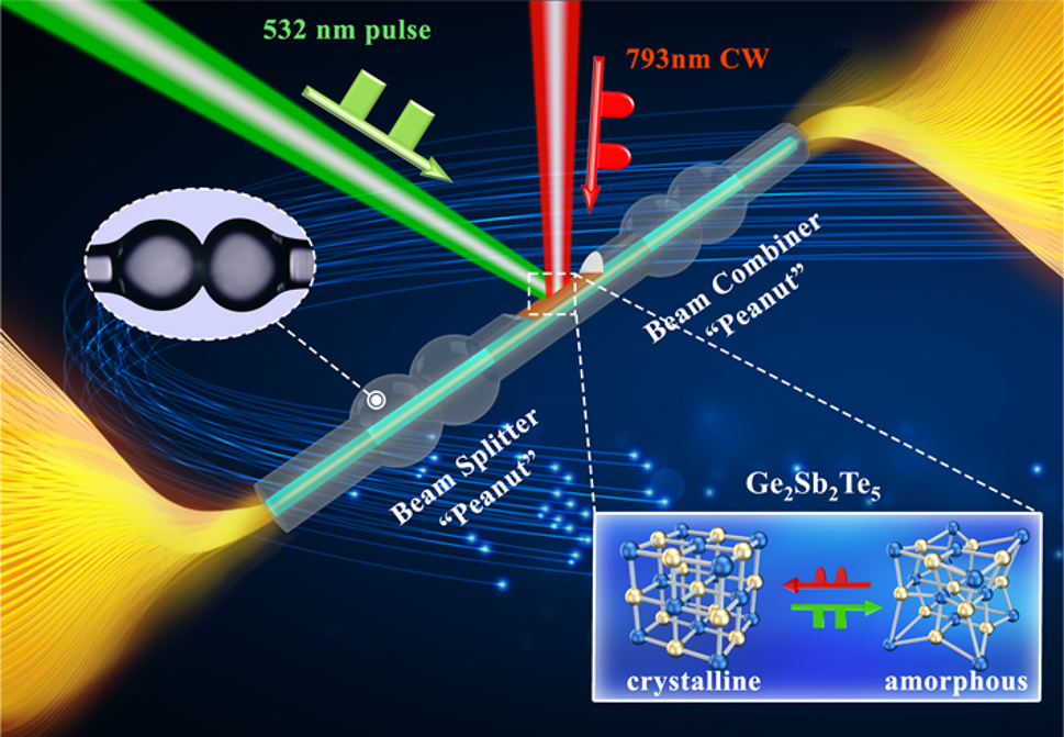
Working principle of the all-optical modulator. The modulator employs a dual peanut-shaped optical fiber structure and GST composition. During the modulation process, modulation information is stored in the GST film coated on the D-shaped side-polished region. The multi-level modulation of the all-optical modulator is accomplished by irradiating the GST film with a 532 nm pulsed laser and a 793 nm CW laser.
2 Construction and characterization of optical switch
Our all-optical modulator is fabricated from single-mode optical fiber (SMF-28). A fiber fusion splicer (Notevio NT-200s) is used to discharge the flat end face of the optical fiber. Under the action of high-voltage electric arcs, the end face of the optical fiber melts, and due to the presence of surface tension, it gradually forms a smooth fiber ball. Subsequently, a low-voltage discharge arc is used to connect two fiber balls, forming a peanut-shaped coupler. Connecting two peanuts in series creates a Mach–Zehnder interferometer (MZI).
In the MZI, light travels along the core of the optical fiber to reach the first “peanut beam splitter,” where light in the core is coupled into the cladding. The optical signal in the core continues to propagate, while the light in the cladding is modulated by GST when passing through the side-etching region. As the light in the cladding and the core passes through the second “peanut coupler,” the light in the cladding is coupled back into the core, causing interference with the light in the core, as shown in Figure 2(a). It is noteworthy that, to increase the interaction area between the optical signal inside the optical fiber and GST, we use a high-frequency carbon dioxide laser to side-etching the interference arm region between the two peanuts. Additionally, a 45 nm-thick layer of GST film is coated in the D-shaped side-etching region using magnetron sputtering. Figure 2(e)–(g) illustrate microscope images of the D-shaped side-etching region in the states of “no GST coating” along the x–z direction, x–y direction, and with GST coating (x–y direction).

Performance and characterization of dual peanut-shaped structure. (a) Schematic diagram illustrating the mechanism of the dual peanut-shaped Mach–Zehnder interferometer (MZI). (b–d) Microscopic images of peanut-shaped MZIs with diameters of 180 μm, 210 μm, and 240 μm, where the lengths of the “peanuts” are 440 μm, 515 μm, and 585 μm, respectively. Microscopic images of the D-shaped side-polished region without GST coating in the x–z plane (e) and x–y plane (f). (g) Microscopic images of the D-shaped side-polished region with GST coating. (h–j) Transmission spectra of the three peanut-shaped MZIs (d = 180 μm, 210 μm, and 240 μm), with interference intensities of 21.67 dB, 14.02 dB, and 11.05 dB, respectively.
In this peanut MZI, φcl and φcore are phases of the cladding mode and core mode:
where λ0 is the central wavelength,
Here, the transmission intensity of our peanut MZI can be defined as:
where I, I1, and I2 are the transmission intensities of the light in the optical path, cladding, and core, respectively. In our MZI measuring system, the transmission intensity and phase shift can be monitored by a high-accuracy optical spectrum analyzer (OSA, AQ6317C, Yokogawa TM resolution of 0.2 nm).
To investigate the impact of peanut diameter on the performance of the all-optical modulator, devices with diameters of 180 μm, 210 μm, and 240 μm were fabricated, as shown in Figure 2(b)–(d). The lengths of the peanut structures (along the x-axis) are 440 μm, 515 μm, and 585 μm, respectively. An ASE broadband light source is used as the probing light, and an OSA is employed to detect the spectra of peanut-shaped interferometers with different diameters, as shown in Figure 2(h)–(j). From the graphs, it can be observed that with the increase in peanut diameter, the interference intensity of the peanut-shaped MZI decreases from 21.67 dB to 11.05 dB. In this study, to obtain a distinctly discernible intermediate state, the interference intensity of the peanut-shaped MZI should be as large as possible. Therefore, we choose the peanut-shaped MZI with a diameter of 180 μm as the core structure for the all-optical modulator.
3 Theoretical and simulation analysis
To investigate the influence of GST in different states on the all-optical modulator, we measured the negative refractive index of both crystalline and amorphous GST using an ellipsometer. Additionally, we employed the time-domain finite element method to simulate the fiber side-etching region. The refractive index of GST was set to the crystalline state (n_c-GST = 6.5 + 1.1k), and the simulated light field distribution is shown in Figure 3(a). As illustrated in Figure 3(b), when the negative refractive index of GST changes to the amorphous state parameters (n_a-GST = 3.9 + 0.02k), a significantly different change occurs in the optical signal inside the fiber. It can be observed that when GST is in the crystalline state, the extinction coefficient of GST increases, and there is significant attenuation of light in the side-etching region. Furthermore, simulations of the light field in the cross-section of the optical side-etching region were conducted. Comparing Figure 3(c) and (d), when GST is in the amorphous state, the light field in the fiber cross-section is concentrated in the central region because the extinction coefficient of GST in the amorphous phase is significantly smaller, and the core mode is undisturbed. As GST transitions to the amorphous state, its extinction coefficient increases, the optical signal inside the fiber is absorbed by GST, and simultaneously, the light field undergoes a shift toward the GST-coated plane.

Simulation of phase-change storage unit. (a–b) Distribution of electric fields in the crystalline, amorphous, and intermediate states of GST. The results indicate that GST can block optical signals within the optical fiber, showing distinct behavior in its two states. (c–d) Simulation of the electric field interface distribution in the D-shaped side-polished region coated with GST material. When GST is in the crystalline state, the energy distribution of the electric field shifts towards c-GST. This suggests that, compared to a-GST, c-GST exhibits a stronger attraction to optical signals. (e) Thermal field distribution in the crystalline state of the D-shaped side-polished region with GST, showing thermal attenuation along the direction of optical signal transmission. (f–g) Thermal field distribution in the D-shaped side-polished region with GST in amorphous and crystalline states, respectively.
Subsequently, we established a three-dimensional model to investigate the temperature characteristics of GST in the operational scenario of the all-optical modulator. The initially crystalline GST coated on the side-etching region was set. As seen in Figure 3(e), the optical signal, upon contact with GST, is absorbed, generating a significant amount of heat that attenuates along the direction of GST. It is observed that the strong absorption effect of crystalline GST leads to the generation of a large amount of heat in the part of GST that first comes into contact with light. This results in the occurrence of “element separation,” “worm surface,” and “surface GST oxidation.” All of which significantly reduce the lifespan of the all-optical modulator. Therefore, we coated a uniform layer of ITO film on the surface of the GST film. The ITO film serves as both a uniform heat-conducting layer and an anti-oxidation layer. Figure 3(f) and (g) show the internal heat distribution of the fiber when GST is in the amorphous and crystalline states, respectively. In particular, the heat distribution trend in the GST-coated region in Figure 3(g) is consistent with that in Figure 3(e).
4 Experimental
To achieve multi-level modulation functionality of the all-optical modulator, a 532 nm pulsed laser and a 793 nm CW laser were used to alternately irradiate the GST film coated on the side-etching region in a D-shaped configuration, as shown in Figure 4. Signal light (HY-ASE-C + L-N-17-BD-FA, CONNECT) and a frequency-swept laser source are sent from the two ports of the first 2 × 1 coupler to a polarization controller (PC), undergoing interference and modulation through the dual-peanut-shaped MZI. An optical spectrum analyzer (OSA) and oscilloscope are employed to monitor the optical signal at the output end of the dual-peanut-shaped MZI. In Figure 5(a) and (b), it can be observed that during the modulation process of the initially crystalline GST film using a 532 nm pulsed laser, as the degree of amorphization of GST increases, the refractive index and extinction coefficient of GST decrease. This leads to a reduction in the effective refractive index in the cladding region and, simultaneously, a decrease in GST’s absorption of light. As a result, the interference peak transmittance of the peanut-shaped MZI increased by 3.3 dB, the extinction ratio increased from 1.3 dB to 7.1 dB, and the transmission spectrum exhibited a blue shift of 1.44 nm.

Optical modulation system setup for the all-optical modulator. An amplified spontaneous emission (ASE) source (A-0002, wavelength: 1,152.5–1,570 nm; Hoyatek Co., Ltd.) is connected to one end of the dual peanut-shaped MZI via a polarization controller (PC). The other end of the dual peanut-shaped MZI is connected to an optical spectrum analyzer (OSA, Yokogawa AQ6370C) with a resolution of 0.02 nm to record the modulated optical signal. A tunable laser source (TLS, Agilent 81940A) and a photodetector (PD, New Focus, Model 2011) are connected to a high-speed digital oscilloscope (DSO, Dggint MSOX-2022A) for monitoring the phase changes in the dual peanut-shaped MZI. The 532 nm pulsed laser and 793 nm CW laser used for modulating GST are coupled into a fiber collimator via a 2 × 1 coupler after passing through the PC, and they irradiate the GST film to achieve modulation.

Multilevel modulation of phase-change storage unit. (a–b) Ten-level transmission spectra of GST with varying degrees of amorphization (crystallization) after irradiation with a 532 nm pulsed laser and a 793 nm CW laser, respectively. (c) Relationship between the output power of the 793 nm CW laser (red line) and the energy of the 532 nm pulsed laser with respect to the modulation level. (d) Independent multi-level states are achieved through probe modulation during four repetitive switching cycles. (e) Intensity fluctuations at different modulation levels over 30 days.
Conversely, when modulating with a 793 nm CW laser, the degree of crystallization of GST increases, leading to an increase in the extinction coefficient and refractive index of GST. This results in an increase in the effective refractive index in the fiber cladding region, intensifying light absorption by GST. Consequently, the transmission spectrum projection intensity of the MZI decreased by 3.7 dB, the extinction ratio decreased from 6.9 dB to 0.8 dB, and the transmission spectrum underwent a redshift of 1.18 nm. Thus, we have achieved the reversible transformation from the “ON” state of “1” to the “OFF” state of “0” in the all-optical modulator.
In Figure 5(c), we present the relationship between the modulation level in the ten-level modulation and the output power of the 793 nm CW laser and the 532 nm pulsed laser, respectively. We observed a correspondence between the output energy of the modulating laser and the modulation levels of GST. When using a 532 nm pulsed laser to induce a ten-level transition of GST from the crystalline state to the amorphous state, the laser output energy levels were 1.35, 1.24, 1.17, 1.08, 0.99, 0.91, 0.83, 0.73, 0.62, and 0.54 mJ, respectively. Similarly, to achieve a ten-level transition from the “ON” state to the “OFF” state in the all-optical modulator, the output power of the 793 nm CW laser was set to ten different levels: 3.45 ± 0.18, 4.22 ± 0.21, 5.03 ± 0.23, 5.83 ± 0.31, 6.65 ± 0.21, 7.48 ± 0.24, 9.08 ± 0.23, 9.84 ± 0.25, 10.70 ± 0.21 mW. This relationship between modulation levels and laser output power facilitates the sequential, reverse, and random modulation of the all-optical modulator. To verify the repeatability of the ten-level all-optical modulator, we conducted four consecutive, complete cycles, each including the crystalline state, amorphous state, and eight stable and distinctly distinguishable intermediate states. As shown in Figure 5(d), under the condition of no external energy maintenance, the all-optical modulator can repeatedly switch between different energy levels, with the transmission intensity differences between the same levels much smaller than those between different levels. Additionally, I conducted stability tests on the all-optical modulator. Over a continuous period of 30 days, we measured and recorded the transmission intensity of 10 energy levels each day, as shown in Figure 5(e). The fluctuation in transmission intensity for each energy level of the all-optical modulator was less than 0.2 dB over the 30-day period. Therefore, the experimental results demonstrated that our all-optical modulator has a very significant non-volatility.
Additionally, we attempted to use the all-optical modulator in the aspect of logic gate computation. Initially, two all-optical modulators, P1 and P2, were connected in series to achieve the “AND” operation, as shown in Figure 6(a). M1 and M2 were defined as the states of GST coated in the side-casting region. It is worth noting that the “AND” gate developed in this work is based on binary operations, so in this study, GST exists in only two states: crystalline (c-GST) and amorphous (a-GST). The transmittance output value of this “AND” gate can be represented as Ta = P1 × P2. To reduce computational errors, GST was modulated to the amorphous state before logic calculations. We used a 532 nm pulse laser with a pulse width of 10 nm and a power of 1.35 mJ, and a 793 nm CW laser with an energy of 3.45 mW to assign the digital “1” and “0”, respectively. We used an ASE light source and a swept laser to read information from the logic gate. We set the reference line to a normalized transmittance (NT) of 60 % (ref = 60 %). When the input terminals of the “AND” gate were given “00”, “10”, “01”, and “11”, the NT at the output terminals of the “AND” gate were “1 %”, “27 %”, “25 %”, and “97 %”, respectively. Therefore, the logical operation results for the four inputs were “0”, “0”, “0”, and “1”, as shown in Figure 6(c) and (e). Similarly, we connected two all-optical modulators, P3 and P4, in series to achieve the “OR” operation, as shown in Figure 6(b). We used two lasers to modulate M3 and M4 to change the input values of the “OR” gate. The transmittance output value of this “OR” gate can be represented as To = P3 + P4. As shown in Figure 6(d) and (f), when the input terminals of the “OR” gate were given “00”, “10”, “01”, and “11”, the NT at the output terminals of the “OR” gate were “5 %”, “64 %”, “67 %”, and “98 %”, respectively. Comparing the output NT values with the reference line, the logical operation results for the four inputs were “0”, “1”, “1”, and “1”.

AND/OR logic computation. (a–b) Schematic representation of the mechanisms of the AND and OR logic gates. The logical AND (OR) operation is achieved by serially connecting (paralleling) two all-optical modulators. (c–d) Truth tables for basic logic AND (OR) operations. Outputs for four different input state combinations (00, 01, 10, 11): “0, 0, 0, 1” (0, 1, 1, 1). (e–f) Normalized transmittance output plots for different input combinations of the modulo-2 logic AND (OR) operations. The logic calculation output NT is above (below) the reference value for logic “1” (“0”).
5 Conclusions
In conclusion, we have presented, for the first time, a fully optical modulator with ten-level controllability, combining GST and a peanut-shaped MZI fiber microstructure. The interference intensity of the MZI can reach 21 dB. External laser modulation using a 532 nm pulse laser and a 793 nm CW laser was employed to adjust the crystalline state of GST. Four consecutive complete cycles were used to demonstrate the significant repeatability of the all-optical modulator. Through continuous monitoring of each level for 30 days at a daily frequency, it was observed that the transmission intensity fluctuations of the all-optical modulator were less than 0.2 dB over the 30-day period, indicating excellent non-volatility. Furthermore, the serial and parallel connection of two all-optical modulators achieved “AND” and “OR” computations. Undoubtedly, this study demonstrates the remarkable capability of a multi-level all-optical modulator with long-distance transmission capacity. This fiber-based all-optical modulator can perform more complex calculations, laying the foundation for high-speed data communication and information exchange in future all-optical networks.
Funding source: Fundamental Research Funds for the Central Universities
Funding source: National Natural Science Foundation of China
Award Identifier / Grant number: 52271344
-
Research funding: This work was supported by National Natural Science Foundation of China (52271344) and Fundamental Research Funds for the Central Universities.
-
Author contributions: JPS: experimental design, optical and system design, proposing innovation, feasibility analysis, experiment advancement. JHM: repeatability verification. JXG: optical path construction. JWW: thermal simulation. YXL: data analysis. WJ: technical support. YZ: manuscript text review. LL: manuscript figure review. HYL: funding support. ZHL: funding support. All authors have accepted responsibility for the entire content of this manuscript and consented to its submission to the journal, reviewed all the results and approved the final version of the manuscript.
-
Conflict of interest: Authors state no conflicts of interest.
-
Data availability: Data underlying the results presented in this paper are not publicly available at this time but may be obtained from the authors upon reasonable request.
References
[1] H. J. Caulfield and S. Dolev, “Why future supercomputing requires optics,” Nat. Photonics, vol. 4, no. 5, pp. 261–263, 2010. https://doi.org/10.1038/nphoton.2010.94.Search in Google Scholar
[2] K. S. Bindra, H. T. Bookey, A. K. Kar, B. S. Wherrett, X. Liu, and A. Jha, “Nonlinear optical properties of chalcogenide glasses: observation of multiphoton absorption,” Appl. Phys. Lett., vol. 79, no. 13, pp. 1939–1941, 2001, https://doi.org/10.1063/1.1402158.Search in Google Scholar
[3] M. Stegmaier, C. Rios, H. Bhaskaran, C. D. Wright, and W. H. P. Pernice, “Nonvolatile all-optical 1 × 2 switch for chip-scale photonic networks,” Adv. Opt. Mater., vol. 5, no. 1, p. 1600346, 2017. https://doi.org/10.1002/adom.201600346.Search in Google Scholar
[4] M. Rakib-Uddin, T. Q. Hoai, B. Nakarmi, and H. W. Yong, “All-optical 1 × 2 switch using Fabry-Perot laser diodes,” IEEE Xplore, vol. 7988, p. 79880B, 2010.10.1117/12.888329Search in Google Scholar
[5] T. Tanabe, M. Notomi, S. Mitsugi, A. Shinya, and E. Kuramochi, “Fast bistable all-optical switch and memory on a silicon photonic crystal on-chip,” Opt. Lett., vol. 30, no. 19, pp. 2575–2577, 2005. https://doi.org/10.1364/ol.30.002575.Search in Google Scholar PubMed
[6] I. Chakraborty, G. Saha, A. Sengupta, and K. Roy, “Toward fast neural computing using all-photonic phase change spiking neurons,” Sci. Rep., vol. 8, no. 1, p. 1, 2018. https://doi.org/10.1038/s41598-018-31365-x.Search in Google Scholar PubMed PubMed Central
[7] J. Faneca, T. D. Bucio, F. Y. Gardes, and A. Baldycheva, “O-band N-rich silicon nitride MZI based on GST,” Appl. Phys. Lett., vol. 116, no. 9, 2020, https://doi.org/10.1063/1.5140350.Search in Google Scholar
[8] A. Liu, et al.., “A high-speed silicon optical modulator based on a metal–oxide–semiconductor capacitor,” Nature, vol. 427, no. 6975, pp. 615–618, 2004. https://doi.org/10.1038/nature02310.Search in Google Scholar PubMed
[9] W. T. Chen, A. Y. Zhu, and F. Capasso, “Flat optics with dispersion-engineered metasurfaces,” Nat. Rev. Mater., vol. 5, no. 8, pp. 604–620, 2020. https://doi.org/10.1038/s41578-020-0203-3.Search in Google Scholar
[10] M. H. R. Lankhorst, B. W. S. M. M. Ketelaars, and R. A. M. Wolters, “Low-cost and nanoscale non-volatile memory concept for future silicon chips,” Nat. Mater., vol. 4, no. 4, pp. 347–352, 2005. https://doi.org/10.1038/nmat1350.Search in Google Scholar PubMed
[11] C. Rios, et al.., “Controlled switching of phase-change materials by evanescent-field coupling in integrated photonics,” Opt. Mater. Express, vol. 8, no. 9, pp. 2455–2470, 2018. https://doi.org/10.1364/ome.8.002455.Search in Google Scholar
[12] R. Irawan, T. S. Chuan, T. C. Meng, and T. K. Ming, “Rapid constructions of microstructures for optical fiber sensors using a commercial CO2 laser system,” Open Biomed. Eng. J., vol. 2, no. 1, pp. 28–35, 2008. https://doi.org/10.2174/1874120700802010028.Search in Google Scholar PubMed PubMed Central
[13] R. Li, et al.., “Photonics for neuromorphic computing: fundamentals, devices, and opportunities,” Adv. Mater., vol. 37, no. 2, p. 2312825, 2025, https://doi.org/10.1002/adma.202312825.Search in Google Scholar PubMed
[14] B. J. Shastri, et al.., “Photonics for artificial intelligence and neuromorphic computing,” Nat. Photonics, vol. 15, no. 2, pp. 102–114, 2021, https://doi.org/10.1038/s41566-020-00754-y.Search in Google Scholar
[15] Z. Ying, et al.., “Electronic-photonic arithmetic logic unit for high-speed computing,” Nat. Commun., vol. 11, no. 1, p. 2154, 2020, https://doi.org/10.1038/s41467-020-16057-3.Search in Google Scholar PubMed PubMed Central
[16] J. P. Laine, B. E. Little, and H. A. Haus, “Etch-eroded fiber coupler for whispering-gallery mode excitation in high-silica microspheres,” IEEE Photonics Technol. Lett., vol. 11, no. 11, pp. 1429–1430, 1999. https://doi.org/10.1109/68.803068.Search in Google Scholar
[17] J. Kim, Y. Yang, T. Badloe, I. Kim, G. Yoon, and J. Rho, “Geometric and physical configurations of meta-atoms for advanced metasurface holography,” InfoMat, vol. 3, no. 7, pp. 739–754, 2021. https://doi.org/10.1002/inf2.12191.Search in Google Scholar
[18] M. Shao, X. G. Qiao, H. W. Fu, N. Zhao, Q. P. Liu, and H. Gao, “An in-fiber Mach–Zehnder interferometer based on arc-induced tapers for high sensitivity humidity sensing,” IEEE Sens. J., vol. 13, no. 5, pp. 2026–2031, 2013. https://doi.org/10.1109/jsen.2013.2247591.Search in Google Scholar
[19] D. Wu, T. Zhu, K. S. Chiang, and M. J. Deng, “All single-mode fiber Mach–Zehnder interferometer based on two peanut-shape structures,” J. Lightwave Technol., vol. 30, no. 5, pp. 805–810, 2012. https://doi.org/10.1109/jlt.2011.2182498.Search in Google Scholar
[20] C. Rios, et al.., “Integrated all-photonic non-volatile multi-level memory,” Nat. Photonics, vol. 9, no. 11, p. 725, 2015. https://doi.org/10.1038/nphoton.2015.182.Search in Google Scholar
[21] B. Gholipour, P. Bastock, C. Craig, K. Khan, D. Hewak, and C. Soci, “Amorphous metal-sulphide microfibers enable photonic synapses for brain-like computing,” Adv. Opt. Mater., vol. 3, no. 5, p. 634, 2015, https://doi.org/10.1002/adom.201400472.Search in Google Scholar
[22] C. Rios, P. Hosseini, C. D. Wright, H. Bhaskaran, and W. H. P. Pernice, “On-chip photonic memory elements employing phase change materials,” Adv. Mater., vol. 26, no. 9, pp. 1372–1377, 2014. https://doi.org/10.1002/adma.201304476.Search in Google Scholar PubMed
[23] H. Zhang, N. Healy, A. F. J. Runge, C. C. Huang, D. W. Hewak, and A. C. Peacock, “Optical-resonance-enhanced nonlinearities in a MoS2-coated single-mode fiber,” Opt. Lett., vol. 43, no. 13, p. 3100, 2018, https://doi.org/10.1364/ol.43.003100.Search in Google Scholar
[24] B. Gholipour, A. Karvounis, J. Yin, C. Soci, K. F. MacDonald, and N. I. Zheludev, “Phase-change-driven dielectric-plasmonic transitions in chalcogenide meta-surfaces,” NPG Asia Mater., vol. 10, no. 6, p. 533, 2018. https://doi.org/10.1038/s41427-018-0043-4.Search in Google Scholar
[25] Q. Wang, et al.., “Optically reconfigurable metasurfaces and photonic devices based on phase change materials,” Nat. Photonics, vol. 10, no. 1, pp. 60–65, 2015, https://doi.org/10.1038/nphoton.2015.247.Search in Google Scholar
[26] A. Pantazi, S. Wozniak, T. Tuma, and E. Eleftheriou, “All-memristive neuromorphic computing with level-tuned neurons,” Nanotechnology, vol. 27, no. 35, 2016, https://doi.org/10.1088/0957-4484/27/35/355205.Search in Google Scholar PubMed
[27] D. Kuzum, R. G. D. Jeyasingh, B. Lee, and H. S. P. Wong, “Nanoelectronic programmable synapses based on phase change materials for brain-inspired computing,” Nano Lett., vol. 12, no. 5, pp. 2179–2186, 2012. https://doi.org/10.1021/nl201040y.Search in Google Scholar PubMed
[28] E. Goulielmakis and T. Brabec, “High harmonic generation in condensed matter,” Nat. Photonics, vol. 16, no. 6, pp. 411–421, 2022, https://doi.org/10.1038/s41566-022-00988-y.Search in Google Scholar
[29] L. B. Shaw, B. Cole, P. A. Thielen, J. S. Sanghera, and I. D. Aggarwal, “Mid-wave IR and long-wave IR laser potential of rare-earth doped chalcogenide glass fiber,” IEEE J. Quantum Electron., vol. 37, no. 9, pp. 1127–1137, 2001, https://doi.org/10.1109/3.945317.Search in Google Scholar
[30] T. Moriyama, H. Kawashima, M. Kuwahara, X. Wang, H. Asakura, and H. Tsuda, “Small-sized Mach-Zehnder interferometer optical switch using thin film Ge2Sb2Te5 phase-change material,” in 2014 Optical Fiber Communications Conference and Exhibiton (OFC), 2014, pp. 1–13.10.1364/OFC.2014.Tu3E.4Search in Google Scholar
[31] H. Taghinejad, et al.., “ITO-based µ-heaters for multi-stage switching of phase-change materials: towards beyond-binary reconfigurable integrated photonics,” Opt. Express, vol. 29, no. 13, pp. 20449–20462, 2021. https://doi.org/10.1364/oe.424676.Search in Google Scholar PubMed
[32] B. J. Eggleton, B. Luther-Davies, and K. Richardson, “Chalcogenide photonics,” Nat. Photonics, vol. 5, no. 3, pp. 141–148, 2011, https://doi.org/10.1038/nphoton.2011.309.Search in Google Scholar
[33] S. Ferrari, O. Kahl, V. Kovalyuk, G. N. Goltsman, A. Korneev, and W. H. P. Pernice, “Waveguide-integrated single- and multi-photon detection at telecom wavelengths using superconducting nanowires,” Appl. Phys. Lett., vol. 106, no. 15, 2015, Art. no. 151101. https://doi.org/10.1063/1.4917166.Search in Google Scholar
[34] G. K. Shirmanesh, R. Sokhoyan, P. C. Wu, and H. A. Atwater, “Electro-optically tunable multifunctional metasurfaces,” ACS Nano, vol. 14, no. 6, pp. 6912–6920, 2020, https://doi.org/10.1021/acsnano.0c01269.Search in Google Scholar PubMed
[35] A. Zong, B. R. Nebgen, S.-C. Lin, J. A. Spies, and M. Zuerch, “Emerging ultrafast techniques for studying quantum materials,” Nat. Rev. Mater., vol. 8, no. 4, pp. 224–240, 2023, https://doi.org/10.1038/s41578-022-00530-0.Search in Google Scholar
[36] Q. L. Bao, et al.., “Broadband graphene polarizer,” Nat. Photonics, vol. 5, no. 7, pp. 411–415, 2011, https://doi.org/10.1038/nphoton.2011.102.Search in Google Scholar
[37] D. Piccinotti, B. Gholipour, J. Yao, K. F. MacDonald, B. E. Hayden, and N. I. Zheludev, “Compositionally controlled plasmonics in amorphous semiconductor metasurfaces,” Opt. Express, vol. 26, no. 16, p. 20861, 2018, https://doi.org/10.1364/oe.26.020861.Search in Google Scholar PubMed
[38] J. Orava, A. L. Greer, B. Gholipour, D. W. Hewak, and C. E. Smith, “Characterization of supercoiled liquid Ge2Sb2Te5 and its crystallization by ultrafast-heating calorimetry,” Nat. Mater., vol. 11, no. 4, pp. 279–283, 2012. https://doi.org/10.1038/nmat3275.Search in Google Scholar PubMed
[39] H. N. Gopalakrishna, et al.., “Tracing spatial confinement in semiconductor quantum dots by high-order harmonic generation,” Phys. Rev. Res., vol. 5, no. 1, p. 013128, 2023, https://doi.org/10.1103/physrevresearch.5.013128.Search in Google Scholar
[40] M. Wuttig and N. Yamada, “Phase-change materials for rewriteable data storage,” Nat. Mater., vol. 6, no. 12, p. 1004, 2007, https://doi.org/10.1038/nmat2009.Search in Google Scholar PubMed
[41] D. O. Ignatyeva, et al.., “All-dielectric magnetic metasurface for advanced light control in dual polarizations combined with high-Q resonances,” Nat. Commun., vol. 11, no. 1, p. 5487, 2020, https://doi.org/10.1038/s41467-020-19310-x.Search in Google Scholar PubMed PubMed Central
[42] C. C. Huang, B. Gholipour, J. Y. Ou, K. Knight, and D. W. Hewak, “Electrical phase change of CVD-grown e thin-film device,” Electron. Lett., vol. 47, no. 4, p. 288, 2011, https://doi.org/10.1049/el.2010.3276.Search in Google Scholar
[43] S. Abdollahramezani, et al.., “Tunable nanophotonics enabled by chalcogenide phase-change materials,” Nanophotonics, vol. 9, no. 5, pp. 1189–1241, 2020. https://doi.org/10.1515/nanoph-2020-0039.Search in Google Scholar
[44] X. D. Wen, et al.., “Analysis and measurement of the displacement sensor based on an up-tapered Mach–Zehnder interferometer,” Chin. Phys. Lett., vol. 31, no. 3, 2014, Art. no. 034203. https://doi.org/10.1088/0256-307x/31/3/034203.Search in Google Scholar
[45] H. Ren, X. Fang, J. Jang, J. Bürger, J. Rho, and S. A. Maier, “Complex-amplitude metasurface-based orbital angular momentum holography in momentum space,” Nat. Nanotechnol., vol. 15, no. 11, pp. 948–955, 2020. https://doi.org/10.1038/s41565-020-0768-4.Search in Google Scholar PubMed
[46] S. Nakamura and K. Tajima, “Analysis of sub-picosecond full-switching with a symmetric Mach-Zehnder all-optical switch,” J. Opt. A: Pure Appl. Opt., vol. 35, no. 11A, pp. 1426–1429, 1996.10.1143/JJAP.35.L1426Search in Google Scholar
[47] M. M. Salary and H. Mosallaei, “Tunable all-dielectric metasurfaces for phase-only modulation of transmitted light based on quasi-bound states in the continuum,” ACS Photonics, vol. 7, no. 7, pp. 1813–1829, 2020, https://doi.org/10.1021/acsphotonics.0c00554.Search in Google Scholar
[48] F. A. Di, et al.., “All-optical free-space routing of upconverted light by metasurfaces via nonlinear interferometry,” Nat. Nanotechnol., vol. 19, no. 3, pp. 298–305, 2024. https://doi.org/10.1038/s41565-023-01549-2.Search in Google Scholar PubMed
[49] G. Yoon, K. Kim, S.-U. Kim, S. Han, H. Lee, and J. Rho, “Printable nanocomposite metalens for high-contrast near-infrared imaging,” ACS Nano, vol. 15, no. 1, pp. 698–706, 2021. https://doi.org/10.1021/acsnano.0c06968.Search in Google Scholar PubMed
[50] K. Tajima, S. Nakamura, and Y. Sugimoto, “Ultrafast polarization discriminating Mach-Zehnder all-optical switch,” Appl. Phys. Lett., vol. 67, no. 25, pp. 3709–3711, 1995, https://doi.org/10.1063/1.115357.Search in Google Scholar
[51] D. Lee, et al.., “Hyperbolic metamaterials: fusing artificial structures to natural 2D materials,” eLight, vol. 2, no. 1, p. 1, 2022. https://doi.org/10.1186/s43593-021-00008-6.Search in Google Scholar
[52] T. Martins, et al.., “Fiber-integrated phase-change reconfigurable optical attenuator,” APL Photonics, vol. 4, no. 11, 2019, Art. no. 111301. https://doi.org/10.1063/1.5116000.Search in Google Scholar
© 2025 the author(s), published by De Gruyter, Berlin/Boston
This work is licensed under the Creative Commons Attribution 4.0 International License.
Articles in the same Issue
- Frontmatter
- Research Articles
- All-photon logic gate calculation based on phase change materials
- Strong broadband intensity noise squeezing from infrared to terahertz frequencies in lasers with nonlinear dissipation
- Optical phased arrays for wavefront shaping in forward scattering media
- Oxygen vacancy-driven bandgap tuning and ultrafast laser performance in Bi2O2Se
- Phase-matched electron–photon interactions enabled by 3D-printed helical waveguides
- Deterministic time rewinding of waves in time-varying media
- Biomaterial-based random lasers achieved from peanut kernel doped with birch leaf–derived carbon dots
- Arbitrary polarization and rotation multiplexed metasurface hologram
- Statistical regimes of electromagnetic wave propagation in randomly time-varying media
- Neural network enabled wide field-of-view imaging with hyperbolic metalenses
- 3-dimensional plasmonic nanomotors enabled by independent integration of optical pulling and lateral forces
- Erratum
- Corrigendum to: Janus metagrating for tailoring direction-dependent wavefronts