Mid-infrared wavelength multiplexers on an InP platform
-
Kevin Zhang

 ,
Rudolf Mayer
,
Rudolf Mayer

Abstract
We demonstrate mid-infrared multiplexers based on evanescent couplers in In0.53Ga0.47As/InP ridge waveguides. Multiplexing of λ = 5.2 µm and λ = 8 µm input wavelengths in TM00 modes to a single TM00 output was achieved with 0.7 dB insertion loss. The demonstrated multiplexing bandwidth is significantly broader than is achievable using typical arrayed waveguide gratings, while displaying comparable insertion loss. These devices will be essential toward the development of broadband multi-color mid-infrared photonic integrated circuits for multi-species gas sensing and multi-band mid-infrared free-space communications.
1 Introduction
Integrating photonic components onto a singular chip is crucial for condensing bulky free-space optical setups into portable mass-producible solutions. Photonic integrated circuit (PIC) technologies in the mid-infrared (mid-IR, λ ≈ 3–25 µm) spectral range are highly sought after for spectroscopic and sensing applications [1], [2], [3], [4], [5], owing to the numerous molecular vibrational “fingerprint” absorption lines found in this region. Additionally, mid-IR light is advantageous for free space communication [6], [7], [8], [9] as it offers longer propagation distances compared to shorter wavelengths, particularly in adverse weather conditions [10], [11].
The predominant semiconductor laser source in the mid-IR is the quantum cascade laser (QCL), providing room temperature high power output within the entire mid-IR spectral range [12], [13], [14], [15]. We have recently experimentally demonstrated the operation of an InP-based mid-IR photonic integrated circuit (PIC) platform based on the monolithic integration of InGaAs/AlInAs/InP QCLs with In0.53Ga0.47As/InP passive waveguides [16], [17]. We have also demonstrated that the passive In0.53Ga0.47As/InP ridge waveguides can be fabricated to possess optical losses as low as 0.5 dB/cm at 5 µm wavelength, and lower than 3 dB/cm up to 10 µm wavelength [4]. Other groups reported similar or even lower mid-IR losses on this platform [18], [19]. This makes the InP platform an ideal materials system to develop broadband mid-IR PICs.
In many instances, one desires to multiplex the outputs of distributed feedback (DFB) QCLs operating at widely spaced wavelengths into a single beam. Examples of applications for such devices include multi-species gas sensing [20] or multi-band free-space communications [21]. It has been shown that the active region of QCLs can combine multiple laser gain sections in a single stack to produce broadly-tunable [22] and multi-color [23], [24], [25], [26] lasers. The emitted light of multiple QCLs on one chip with different emission wavelengths could then be combined to a singular output waveguide using a passive wavelength multiplexer integrated monolithically on the same InP chip.
Wavelength division multiplexing is typically done using arrayed waveguide gratings (AWGs). This architecture allows for multiplexing of a dense arrangement of wavelengths within a narrowband spectral range which is ideal for telecommunications applications. Multiplexing using AWGs has also been demonstrated in the mid-IR recently at λ ≈ 5.2 µm [27]. However, for spectroscopic applications, sometimes a more sparse arrangement of wavelengths may be required, but within a very broad spectral band. Additionally, applications such as remote sensing or free space communications often aim to utilize the atmospheric transparency windows at both 3–5 μm and 8–12 μm bands. To this end, here we use In0.53Ga0.47As/InP waveguiding platform to experimentally demonstrate wavelength division multiplexers using evanescent waveguide couplers [28], [29], capable of multiplexing λ ≈ 5.2 and λ ≈ 8 µm with an insertion loss of around 0.7 dB. While only two wavelengths were multiplexed in this work, additional evanescent couplers may be independently designed for other wavelengths and fabricated in series to combine an arbitrary number of inputs. Our results indicate that this multiplexing scheme on an InP platform holds much promise for the future development of PICs in the mid-IR.
2 Multiplexer design
Simulations of waveguide geometries were performed using a finite difference time domain (FDTD) solver, Ansys Lumerical. Given the transverse magnetic (TM) output of QCLs, simulations and experimental measurements reported here focused on TM-polarized modes. The refractive index data for all materials was characterized based on reflectance measurements of thin films grown in house using molecular beam epitaxy (MBE). Propagation losses of these materials has been assumed to be identical to those shown in Ref. [4] due to both samples being grown in the same MBE in house and fabricated with identical fabrication procedures. A pair of identical waveguides are then simulated together with a variable separation, d, as shown in Figure 1. At a small enough separation, these two waveguides become coupled, causing a periodic transfer of power between the two. An eigensolver is used to calculate the coupled symmetric and anti-symmetric modes. The index difference between this pair of fundamental coupled modes for every wavelength can be used to determine the period of power transfer between the waveguides using the following expression [30]:
where Pout is the power in the secondary waveguide, Pin is the power in the origin waveguide, L is the coupling length, Δn is the effective refractive index difference between the symmetric and anti-symmetric coupled modes, and λ is the wavelength. To minimize insertion loss due to optical absorption, the coupler length is minimized while maintaining 100 % power transfer into the secondary waveguide.

A 2 x 1 evanescent coupler. (a) Schematic. (b) Simulated propagation of a λ = 8 μm wave through an evanescent coupling region designed for 100 % power transfer to the upper waveguide. (c) Simulated propagation of a λ = 5.2 μm wave passing through the same coupling region unimpeded.
The coupling strength between the two waveguides, as represented by Δn, is shown in Figure 2d for this particular waveguide geometry for different separation distances for both λ = 5.2 μm and 8 μm wavelengths. In this method of wavelength multiplexing, the large spectral separation in the wavelengths to be multiplexed is taken advantage of in order to reduce cross talk between channels. Due to the larger mode size of the longer wavelength mode, a waveguide geometry can be chosen such that the shorter wavelength experiences virtually no coupling, while the long wavelength experiences strong coupling. This can be seen in Figure 2d, where the Δn of the λ = 5.2 μm mode stays near zero, while the Δn of the λ = 8 μm is at least two orders of magnitude larger for waveguide separation distances below 1 μm. As a result, the channel with the shorter wavelength continues unimpeded to the waveguide output facet, while the longer wavelength is multiplexed into the other channel, as shown in Figure 1b and c. When cascading more than one evanescent coupler together, wavelengths must be multiplexed in order of increasing wavelength to avoid channel crosstalk. To achieve sufficient mode coupling while maintaining adequate mode confinement, the waveguide was constructed with a 1.5-μm-thick undoped In0.53Ga0.47As core, surrounded on top and bottom by 3-μm-thick cladding layers of undoped InP. A waveguide width of 5 μm was chosen. Figure 2c presents the computed effective refractive index and group index for the fundamental TE and TM mode as a function of the mid-IR wavelength for ridge-waveguides with this geometry. The calculated symmetric and antisymmetric mode profiles for this geometry is shown in Figure 2a and b for λ = 8 μm. Due to fabrication constraints, a waveguide separation narrower than 1 μm can pose significant challenges. Therefore, the minimum gap size of d = 1 μm was chosen, and a coupling length of L = 430 μm was calculated.
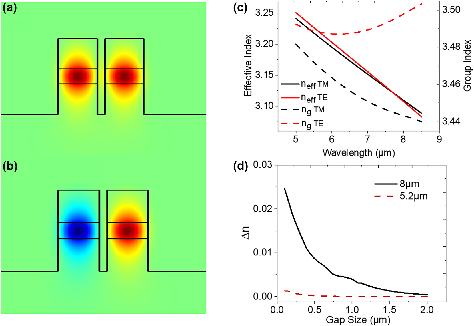
Simulated (a) symmetric and (b) antisymmetric mode for a parallel propagating waveguide pair with 1.5 μm In0.53Ga0.47As core thickness, 3 μm InP:Fe upper and lower cladding, 5 μm width, and 1 μm separation at λ = 8 μm. (c) Simulated values of the effective refractive index and group index for the given waveguide geometry for both the fundamental TE and TM modes. (d) Simulated values of Δn for the same coupled waveguide structure as a function of separation distance for both λ = 5.2 μm and 8 μm.
3 Experimental section
3.1 Device fabrication
The material layers for the waveguide structure are epitaxially grown on a semi-insulating InP:Fe substrate. The iron compensation significantly reduces the optical losses of the material by trapping free carriers [31]. This substrate is used as the lower cladding of the ridge waveguide structure. On top of the substrate, a layer of nominally undoped lattice-matched In0.53Ga0.47As with a background doping concentration of n = 7 × 1014 cm−3 is grown with molecular beam epitaxy (MBE). Finally, another layer of nominally undoped InP with a background doping of n = 5 × 1015 cm−3 is grown with MBE on top as the upper cladding of the three-layered waveguide. These materials are all capable of being homogeneously integrated with QCLs and are transparent for the desired mid-IR region. Background carrier concentrations in the core and cladding layers were computed to produce smaller than 0.5 dB/cm propagation loss [4].
Devices are defined using electron beam lithography. The mask pattern was transferred to a Si x N y hard mask using a CF4/O2 plasma in an inductively coupled plasma reactive ion etching system (ICP-RIE). This was then transferred into the semiconductor layers using a CH4/H2 plasma in an ICP-RIE. Residual hard mask was removed using another CF4/O2 plasma etch. Waveguide facets were cleaved to expose input and output facets for external in and out-coupling of light. A multi-layer antireflection coating composed of alternating YF3 and ZnS layers was then evaporated onto both facets in order to suppress Fabry–Perot oscillations of the waveguides when measuring with narrow linewidth laser sources.
Figure 3a shows a cross sectional scanning electron microscope (SEM) image of a device which has been cleaved through the coupling region. It can be seen that, due to a difference in the mass flow in RIE, the outsides of the waveguides have different etch depths compared to the coupling region. This fabrication imperfection results in a small amount of the transmitted optical power at 8 μm wavelength being in the TE-rather than TM-polarized mode as described in the following.
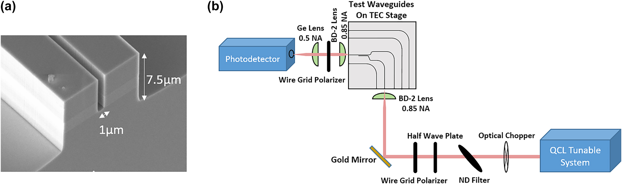
Characterization of fabricated multiplexers. (a) Cross sectional SEM image of the coupling region of an evanescent coupler. The separation gap between the two parallel running waveguides is etched only to the bottom of the In0.53Ga0.47As core (lighter grey color in the image), while the outside of the waveguides is etched 3 μm deep into InP:Fe substrate. (b) Schematic of the experimental setup used to characterize the evanescent couplers.
3.2 Device characterization
The experimental setup used to characterize the evanescent couplers is shown in Figure 3b. Based on measurements of the Fabry–Perot resonances of similar waveguides as a function of sample temperature, we estimate the effective thermo-optic coefficient of our waveguides to be approximately
Each device is composed of two input and one output waveguide. Both input waveguides have an input facet to allow for external light coupling. One of the input waveguides terminates with a taper at the end of the evanescent coupler and the other continues to the output facet of the sample, as shown in Figure 1b. A 90-degree bend is placed before the evanescent coupler, to prevent light not coupled to the waveguide from reaching the detector, as shown in the schematic of the sample in Figure 3b. The sample also contains continuous 90-degree-bent reference waveguides with the same dimensions and the same input tapers as the waveguides used in the coupler as shown in Figure 3b.
Light was first coupled into a reference waveguide adjacent to the coupler device inputs. The transmission through this waveguide was used as a reference in order to approximately normalize out the losses due to material absorption and scattering. While this method of normalization may be subject to inconsistencies with alignment and coupling efficiency, through repetitive alignment to a singular waveguide, we estimate we are able to achieve identical in/out-coupling efficiency to a waveguide with a standard deviation of the total insertion loss of approximately 5 %.
4 Results and discussion
The results of the measured coupler performance versus simulated results are shown in Figure 4, which shows the transmitted optical power through the coupler as a function of wavelength. Several wavelengths within the tuning range of the input laser were tested for both inputs. At the design wavelength of 5.2 μm, the multiplexers achieve a transmitted efficiency of nearly 100 %. The multiplexer is relatively broadband, with a 3 dB cutoff wavelength at λ3dB ≈ 7 μm. Similarly, in the 8 μm channel, the multiplexers exhibit a transmitted efficiency of approximately 86 %, or an insertion loss of 0.7 dB with a 3 dB cutoff wavelength also at approximately 7 μm.
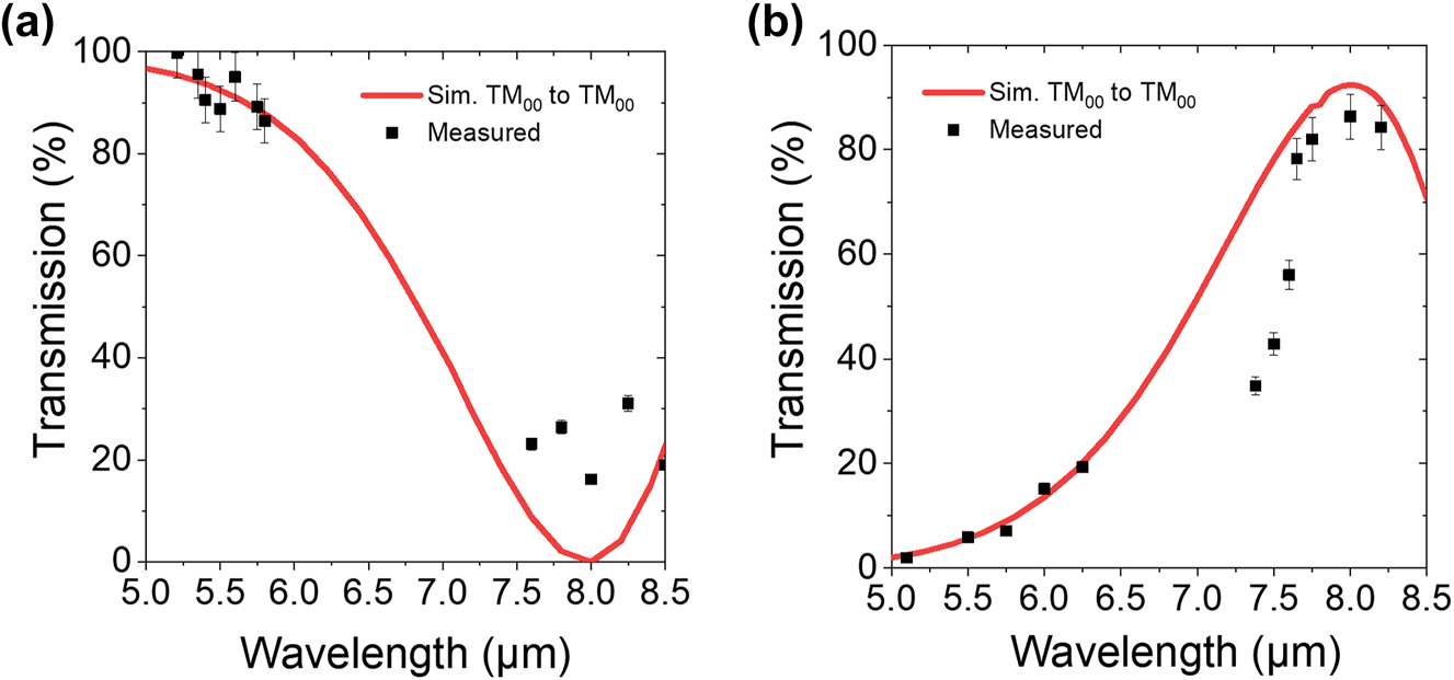
Simulated and measured transmission characteristics of the fabricated evanescent coupler. Total coupler transmission as a function of input wavelength on the (a) λ = 5.2 μm input branch and the (b) λ = 8 μm branch.
As mentioned earlier, due to incomplete etching of the gap between the two waveguides in the coupling section of our device, we expect a small amount of polarization conversion for the optical power sent into the 8 μm input of the coupler. Simulations show that this small amount of polarization-converted signal will be coupled to the TE00 mode in the output waveguide, while coupling to higher-order TE and TM modes are not expected to play a significant role. By inserting a polarizer at the output of the waveguide, as shown in Figure 3, we can isolate the output from any cross polarization. This new data is shown in Figure 5a and b in comparison with simulation results. Additionally, by utilizing a taper at the end of the evanescent coupler we can ensure minimal back reflection, avoiding any disruptive optical feedback toward the light source.
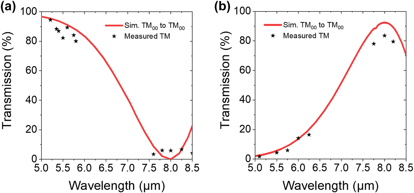
Simulated and measured TM00 polarized coupler transmission as a function of input wavelength on the (a) λ = 5.2 μm input branch and the (b) λ = 8 μm branch.
Compared to the arrayed waveguide gratings demonstrated at λ ≈ 5.2 µm in the same material system [27], coupling losses were comparable at ∼0.9 dB. However, as stated previously, the arrayed waveguide grating method of multiplexing is more suitable for combining wavelengths within a relatively narrow spectral band. Conversely, evanescent coupling allows us to combine discrete wavelengths that can be spaced arbitrarily far apart, allowing for photonic integrated chips capable of targeting spectrally distinct gas absorption lines or atmospheric transparency windows spread throughout the entire mid-infrared spectral range on a single chip.
5 Conclusions
In summary, we report the first mid-IR waveguide multiplexer based on evanescent couplers on an InP/InGaAs based platform which are capable of combining wavelengths as broadly spaced as λ = 8 μm and 5.2 μm, with an efficiency of over 86 %. The efficiency of these devices paired together with the compatibility of this material system with the predominant QCL architecture, opens the door for the production of multi-color mid-IR photonic integrated circuits for applications such as multi-species gas sensing or multi-band free-space communications or light detection and ranging.
Funding source: H2020 Industrial Leadership
Award Identifier / Grant number: 101016956
Funding source: Deutsche Forschungsgemeinschaft
Award Identifier / Grant number: 463411319
-
Research funding: This work was supported by the EC| H2020 | H2020 Industrial Leadership (IL) PASSEPARTOUT project grant number 101016956 and by the German Research Foundation (DFG) grant number 463411319.
-
Author contributions: KZ conceived and designed the study. KZ and RM collected and analyzed the data. KZ, RM, and DB interpreted the results. GB contributed essential materials and resources. KZ drafted the initial manuscript. MAB provided supervision and revision of the manuscript. All authors have accepted responsibility for the entire content of this manuscript and consented to its submission to the journal, reviewed all the results and approved the final version of the manuscript.
-
Conflict of interest: Authors state no conflict of interest.
-
Data availability: The datasets generated and/or analysed during the current study are available from the corresponding author upon reasonable request.
References
[1] U. Willer, M. Saraji, A. Khorsandi, P. Geiser, and W. Schade, “Near- and mid-infrared laser monitoring of industrial processes, environment and security applications,” Opt. Lasers Eng., vol. 44, no. 7, pp. 699–710, 2006. https://doi.org/10.1016/j.optlaseng.2005.04.015.Search in Google Scholar
[2] L. Hvozdara, N. Pennington, M. Kraft, M. Karlowatz, and B. Mizaikoff, “Quantum cascade lasers for mid-infrared spectroscopy,” Vib. Spectrosc., vol. 30, no. 1, pp. 53–58, 2002. https://doi.org/10.1016/S0924-2031(02)00038-3.Search in Google Scholar
[3] V. Spagnolo, P. Patimisco, S. Borri, G. Scamarcio, B. E. Bernacki, and J. Kriesel, “Mid-infrared fiber-coupled QCL-QEPAS sensor,” Appl. Phys. B: Lasers Opt., vol. 112, no. 1, pp. 25–33, 2013. https://doi.org/10.1007/s00340-013-5388-3.Search in Google Scholar
[4] K. Zhang, G. Böhm, and M. A. Belkin, “Mid-infrared microring resonators and optical waveguides on an InP platform,” Appl. Phys. Lett., vol. 120, no. 6, 2022, Art. no. 061106. https://doi.org/10.1063/5.0077394.Search in Google Scholar
[5] M. Troccoli, et al.., “High-performance quantum cascade lasers grown by metal-organic vapor phase epitaxy and their applications to trace gas sensing,” J. Lightwave Technol., vol. 26, no. 21, pp. 3534–3555, 2008. https://doi.org/10.1109/JLT.2008.925056.Search in Google Scholar
[6] M. Joharifar, et al.., “High-Speed 9.6-μm long-wave infrared free-space transmission with a directly-modulated QCL and a fully-passive QCD,” J. Lightwave Technol., vol. 41, no. 4, pp. 1087–1094, 2023. https://doi.org/10.1109/JLT.2022.3207010.Search in Google Scholar
[7] R. Martini, et al.., “High-speed digital data transmission using mid-infrared quantum cascade lasers,” Electron. Lett., vol. 37, no. 21, pp. 1290–1292, 2001. https://doi.org/10.1049/el:20010884.10.1049/el:20010884Search in Google Scholar
[8] S. Blaser, W. Kolosowski, J. Mikolajczyk, and J. Faist, “Free-space optical data link using Peltier-cooled quantum cascade laser,” Electron. Lett., vol. 37, no. 12, pp. 778–780, 2001. https://doi.org/10.1049/el:20010504.10.1049/el:20010504Search in Google Scholar
[9] M. Joharifar, et al.., “Advancing LWIR FSO communication through high-speed multilevel signals and directly modulated quantum cascade lasers,” Opt. Express, vol. 32, no. 17, pp. 29138–29148, 2024. https://doi.org/10.1364/oe.530228.Search in Google Scholar PubMed
[10] A. Arnulf, J. Bricard, E. Curé, and C. Véret, “Transmission by haze and fog in the spectral region 0.35 to 10 microns,” J. Opt. Soc. Am., vol. 47, no. 6, pp. 491–498, 1957. https://doi.org/10.1364/JOSA.47.000491.Search in Google Scholar
[11] P. Corrigan, R. Martini, E. A. Whittaker, and C. Bethea, “Quantum cascade lasers and the Kruse model in free space optical communication,” Opt. Express, vol. 17, no. 6, p. 4355, 2009. https://doi.org/10.1364/oe.17.004355.Search in Google Scholar PubMed
[12] F. Capasso, “High-performance midinfrared quantum cascade lasers,” Opt. Eng., vol. 49, no. 11, 2010, Art. no. 111102. https://doi.org/10.1117/1.3505844.Search in Google Scholar
[13] M. S. Vitiello, G. Scalari, B. Williams, and P. De Natale, “Quantum cascade lasers: 20 years of challenges,” Opt. Express, vol. 23, no. 4, pp. 5167–5182, 2015. https://doi.org/10.1364/oe.23.005167.Search in Google Scholar PubMed
[14] M. Razeghi, W. Zhou, S. Slivken, Q.-Y. Lu, D. Wu, and R. McClintock, “Recent progress of quantum cascade laser research from 3 to 12 μm at the Center for Quantum Devices [Invited],” Appl. Opt., vol. 56, no. 31, pp. H30–H44, 2017. https://doi.org/10.1364/ao.56.000h30.Search in Google Scholar
[15] J. Faist, Quantum Cascade Lasers, Oxford, UK, Oxford University Press, 2013.10.1093/acprof:oso/9780198528241.001.0001Search in Google Scholar
[16] S. Jung, et al.., “Homogeneous photonic integration of mid-infrared quantum cascade lasers with low-loss passive waveguides on an InP platform,” Optica, vol. 6, no. 8, pp. 1023–1030, 2019. https://doi.org/10.1364/optica.6.001023.Search in Google Scholar
[17] D. Burghart, K. Zhang, W. Oberhausen, A. Köninger, G. Boehm, and M. A. Belkin, “Multi-color photonic integrated circuits based on homogeneous integration of quantum cascade lasers,” Nat Commun, vol. 16, p. 3563, 2025. Available at: https://doi.org/10.1038/s41467-025-58905-0.Search in Google Scholar PubMed PubMed Central
[18] R. Wang, P. Täschler, Z. Wang, E. Gini, M. Beck, and J. Faist, “Monolithic integration of mid-infrared quantum cascade lasers and frequency combs with passive waveguides,” ACS Photonics, vol. 9, no. 2, pp. 426–431, 2022. https://doi.org/10.1021/acsphotonics.1c01767.Search in Google Scholar
[19] M. Montesinos-Ballester, et al.., “Low-loss buried InGaAs/InP integrated waveguides in the long-wave infrared,” ACS Photonics, vol. 11, no. 6, pp. 2236–2241, 2024. https://doi.org/10.1021/acsphotonics.3c01898.Search in Google Scholar PubMed PubMed Central
[20] P. Patimisco, et al.., “Quartz-enhanced photoacoustic sensor based on a multi-laser source for in-sequence detection of NO2, SO2, and NH3,” Sensors, vol. 23, no. 21, p. 9005, 2023. https://doi.org/10.3390/s23219005.Search in Google Scholar PubMed PubMed Central
[21] L. Flannigan, L. Yoell, and C. Q. Xu, “Mid-wave and long-wave infrared transmitters and detectors for optical satellite communications – a review,” J. Opt., vol. 24, no. 4, 2022, Art. no. 043002. https://doi.org/10.1088/2040-8986/ac56b6.Search in Google Scholar
[22] N. Bandyopadhyay, M. Chen, S. Sengupta, S. Slivken, and M. Razeghi, “Ultra-broadband quantum cascade laser, tunable over 760 cm^−1, with balanced gain,” Opt. Express, vol. 23, no. 16, 2015, Art. no. 21159. https://doi.org/10.1364/oe.23.021159.Search in Google Scholar
[23] F. Kapsalidis, et al.., “Dual-wavelength DFB quantum cascade lasers: sources for multi-species trace gas spectroscopy,” Appl. Phys. B: Lasers Opt., vol. 124, no. 107, 2018. https://doi.org/10.1007/s00340-018-6973-2.Search in Google Scholar
[24] K. Fujita, et al.., “Recent progress in terahertz difference-frequency quantum cascade laser sources,” Nanophotonics, vol. 7, no. 11, pp. 1795–1817, 2018. https://doi.org/10.1515/nanoph-2018-0093.Search in Google Scholar
[25] A. Jiang, S. Jung, Y. Jiang, K. Vijayraghavan, J. H. Kim, and M. A. Belkin, “Widely tunable terahertz source based on intra-cavity frequency mixing in quantum cascade laser arrays,” Appl. Phys. Lett., vol. 106, no. 26, 2015, Art. no. 261107. https://doi.org/10.1063/1.4923374.Search in Google Scholar
[26] A. Straub, C. Gmachl, D. L. Sivco, A. M. Sergent, F. Capasso, and A. Y. Cho, “Simultaneously at two wavelengths (5.0 and 7.5 μm) single mode and tunable quantum cascade distributed feedback lasers,” Electron. Lett., vol. 38, no. 12, pp. 565–567, 2002. https://doi.org/10.1049/el:20020355.10.1049/el:20020355Search in Google Scholar
[27] T. S. Karnik, et al.., “High-efficiency mid-infrared InGaAs/InP arrayed waveguide gratings,” Opt. Express, vol. 31, no. 3, pp. 5056–5068, 2023. https://doi.org/10.1364/OE.480704.Search in Google Scholar PubMed
[28] S. Somekh, E. Garmire, A. Yariv, H. L. Garvin, and R. G. Hunsperger, “Channel optical waveguide directional couplers,” Appl. Phys. Lett., vol. 22, no. 2, pp. 46–47, 1973. https://doi.org/10.1063/1.1654468.Search in Google Scholar
[29] M. Shamonin, M. Lohmeyer, and P. Hertel, “Directional coupler based on radiatively coupled waveguides,” Appl. Opt., vol. 36, no. 3, pp. 635–641, 1997. https://doi.org/10.1364/ao.36.000635.Search in Google Scholar PubMed
[30] A. Yariv, “Coupled-mode theory for guided-wave optics,” IEEE J. Quantum Electron., vol. 9, no. 9, pp. 919–933, 1973. https://doi.org/10.1109/JQE.1973.1077767.Search in Google Scholar
[31] L. N. Alyabyeva, E. S. Zhukova, M. A. Belkin, and B. P. Gorshunov, “Dielectric properties of semi-insulating Fe-doped InP in the terahertz spectral region,” Sci. Rep., vol. 7, no. 1, pp. 1–7, 2017. https://doi.org/10.1038/s41598-017-07164-1.Search in Google Scholar PubMed PubMed Central
© 2025 the author(s), published by De Gruyter, Berlin/Boston
This work is licensed under the Creative Commons Attribution 4.0 International License.