Free-electron coupling to surface polaritons mediated by small scatterers
-
Leila Prelat
 ,
Eduardo J. C. Dias
and
F. Javier García de Abajo
,
Eduardo J. C. Dias
and
F. Javier García de Abajo


Abstract
The ability of surface polaritons (SPs) to enhance and manipulate light fields down to deep-subwavelength length scales enables applications in optical sensing and nonlinear optics at the nanoscale. However, the wavelength mismatch between light and SPs prevents direct optical excitation of surface-bound modes, thereby limiting the widespread development of SP-based photonics. Free electrons are a natural choice to directly excite strongly confined SPs because they can supply field components of high momentum at designated positions with subnanometer precision. Here, we theoretically explore free-electron–SP coupling mediated by small scatterers and show that low-energy electrons can efficiently excite surface modes with a maximum probability reached at an optimum surface–scatterer distance. By aligning the electron beam with a periodic array of scatterers placed near a polariton-supporting interface, in-plane Smith–Purcell emission results in the excitation of surface modes along well-defined directions. Our results support using scattering elements to excite SPs with low-energy electrons.
1 Introduction
Surface polaritons (SPs) are collective charge oscillations occurring at the interfaces of a wide range of materials and offering a platform to control light–matter interactions at the nanoscale [1], [2]. Specifically, surface-bound optical modes allow us to concentrate electromagnetic energy down to deep-subwavelength length scales and produce large enhancements of the associated near electric fields [3]. Polaritons in two-dimensional (2D) materials are particularly promising because they are highly confined [4], [5] and can be widely controlled by external stimuli introduced through electrical gating [6], [7], [8], [9], chemical doping [10], [11], magnetic fields [12], or optical heating [13], [14], [15], [16]. These appealing properties enable technological applications in areas such as biosensing [17], [18], [19], [20], photodetection [21], [22], [23], light harvesting [24], [25], nonlinear optics [15], [26], [27], [28], and optoelectronics [29], [30], [31].
Unfortunately, strong field confinement in SPs comes at a price, as these modes cannot be directly excited by far-field radiation due to the kinematical mismatch that maintains them trapped to the surface. This problem limits practical applications of SPs, so much effort has been devoted to tackling it through different approaches, including the use of prisms [32] and nanotips [33], [34]. However, prisms are impractical when the SP in-plane wavelength λ
p is small compared with the light wavelength λ
0 = 2πc/ω at the same frequency ω because of the lack of materials with sufficiently high refractive index
As an alternative, electron beams (e-beams) combine high spatial precision with an efficient coupling to SPs [41]. These probes were instrumental in pioneering studies of surface plasmons [42], [43] and are currently reaching a simultaneous spectral/spatial resolution in the few-meV/sub-nm range using techniques such as electron energy-loss spectroscopy [44], [45], [46], [47], [48], [49], [50], [51], [52], [53], [54] (EELS) and photon-induced near-field electron microscopy (PINEM) [55], [56], [57], [58], [59], [60], [61], [62], [63], [64], [65], [66], [67], [68], [69]. The detection of cathodoluminescence light emission resulting from the e-beam interaction with a specimen at a nanometer-controlled position also permits studying bright modes with a spectral resolution depending on the optical spectrometer and the signal-to-noise ratio [70], [71]. Recently, within the emerging field of ultrafast electron microscopy, a temporal resolution in the sub-fs regime [58], [72], [73] has become a possibility by teaming up pulsed lasers and free electrons, while also enabling electron spectromicroscopy to be performed with sub-nm/sub-meV resolution [74], [75]. It should be noted that e-beams effectively act as broadband nanoscale optical sources and, therefore, lack mode selectivity. In particular, an electron moving with velocity v parallel to a polariton-supporting planar surface can excite a wide spectrum of modes satisfying the condition ω < k ‖ v, where ω and k ‖ are the mode frequency and total in-plane wave vector, respectively. In this configuration, the emission is delocalized along the electron interaction path, and relativistic electrons are needed to excite SPs whose dispersion lies close to the light cone. These limitations could be potentially addressed by combining electron excitation with small structures placed in the vicinity of the surface and acting as coupling elements.
In this article, we theoretically explore the excitation of SPs in planar surfaces by parallel e-beams assisted by small scatterers. Specifically, we obtain a clean SP signal by operating under conditions in which electrons cannot directly excite surface modes (i.e., for ω > k ‖ v), so that the scatterers act as intermediate elements where a dipole is induced containing the high-momentum components that are needed to excite SPs. With this approach, narrow-band SP emission can be realized if the scatterer features a spectrally localized mode. We demonstrate that the SP excitation efficiency can be maximized when the scatterer is placed at an optimum distance from the surface, as illustrated by studying the generation of surface-plasmon polaritons (SPPs) in a thin film (e.g., graphene and atomically thin metal layers). Perfectly resonant scatterers and hBN disks are considered. The latter constitute a practical realization of deep-subwavelength resonant scatterers operating in the mid-infrared spectral region. We further extend the phenomenon of Smith–Purcell emission [76] from photons to polaritons by placing a periodic particle array above a polariton-supporting surface and exciting it by a parallel e-beam, leading to the generation of collimated SPs at angles depending on the periodicity, the electron velocity, and the mode dispersion relation. Like in the individual particle, an optimum scatterer–surface distance is also obtained for polaritonic Smith–Purcell emission. These results pave the way for using free electrons combined with small scatterers to control the generation of polaritons in planar surfaces.
2 Electron excitation of surface polaritons mediated by a dipolar particle
We consider the interaction between a fast electron and an individual dipolar scatterer placed at the origin (r = 0), at a distance z
0 away from a planar surface lying at the z = −z
0 plane, as schematically sketched in Figure 1(a). The electron moves parallel to the surface with a velocity
![Figure 1:
Free-electron excitation of surface polaritons (SPs) mediated by a dipolar scatterer. (a) Geometry under consideration, consisting of an electron moving with velocity v parallel to a polariton-supporting surface (a film placed at z = −z
0 supported on a substrate of real permittivity ϵ) and passing above a small particle placed at r = 0 (at a distance b from the trajectory and z
0 from the surface). The electron induces a dipole p on the particle, which couples to the SPs. The particle is in the plane defined by v and the surface normal. (b) Dispersion relation of surface-plasmon polaritons (SPPs)
ω
/
ω
D
=
k
‖
/
k
D
$\omega /{\omega }_{\text{D}}=\sqrt{{k}_{{\Vert}}/{k}_{\text{D}}}$
for a 2D film described by a Drude conductivity of weight ω
D [Eq. (10)] with k
D = (ϵ + 1)ℏω
D/4πe
2 (e.g., ω
D = E
F/πℏ for graphene) compared with the electron line ω = k
‖
v. Both curves intersect at ω/ω
D = v
0/v, where v
0 = ω
D/k
D ≈ 0.092 c/(ϵ + 1). We take v = 1.1 v
0. (c) Spectrally resolved probability of SPP emission ΓSP(ω) under the conditions of (a, b) as a function of excitation frequency ω and particle–surface separation z
0 for fixed k
D
b = 0.1 (e.g.,
z
0
≈
9.5
${z}_{0}\approx 9.5$
nm for self-standing graphene with E
F = 0.3 eV). We assume a lossless resonant scatterer and normalize ΓSP(ω) to the EELS probability ΓEELS(ω) in the absence of the 2D layer [Eq. (16)], ω to ω
D, and z
0 to the SPP wavelength λ
p. (d) Maximum ΓSP(ω) along the yellow curve in (c) (left vertical scale) and normalized optimum separation k
D
z
0 (right scale) as a function of frequency.](/document/doi/10.1515/nanoph-2024-0326/asset/graphic/j_nanoph-2024-0326_fig_001.jpg)
Free-electron excitation of surface polaritons (SPs) mediated by a dipolar scatterer. (a) Geometry under consideration, consisting of an electron moving with velocity v parallel to a polariton-supporting surface (a film placed at z = −z
0 supported on a substrate of real permittivity ϵ) and passing above a small particle placed at r = 0 (at a distance b from the trajectory and z
0 from the surface). The electron induces a dipole p on the particle, which couples to the SPs. The particle is in the plane defined by v and the surface normal. (b) Dispersion relation of surface-plasmon polaritons (SPPs)
The electron can directly excite SPs (without the presence of a scatterer) under the condition that the line ω = k ‖ v lies above the mode dispersion curve in k ‖ − ω space [i.e., for energies above the crossing point in Figure 1(b)]. While the interplay between direct and particle-assisted SP creation constitutes an interesting scenario for future analysis, we limit the present work to frequencies ω below the SP excitation threshold (i.e., direct SP excitation by the electron is kinematically forbidden, but SPs can still be created through the mediation of particle polarization).
2.1 Electron field near a planar surface
Working in frequency space ω, the electric field directly created by the electron as it moves in free space can be written as [77]
where
The presence of the planar surface at z = −z
0 produces a reflected field that can be conveniently expressed in terms of Fresnel’s reflection coefficients
for z < b (i.e., it consists of downward waves emanating from the e-beam). By applying the reflection coefficients to each wave vector and polarization component, the reflected field in the z > − z 0 region above the surface is found to be
The total field generated by the electron in the presence of the surface then becomes
2.2 Self-consistent particle-near-surface response
The field generated by the electron polarizes the dipolar particle placed at the origin, which displays a dipole moment
in the frequency domain. Here,
We follow a similar procedure as with the electron field to express
where s = sign{z}. The surface-reflected field is then obtained by introducing the reflection coefficients as
Finally, setting r = 0 (the dipole position) and carrying out the azimuthal integral in k ‖, we find
in terms of a Green tensor
Combining this result with Eq. (3), we can write the self-consistently induced dipole as
where
is an effective polarizability that takes into account the effect of the surface, so only the electron field is now required to evaluate the induced dipole [cf. Eqs. (3) and (6a)]. Incidentally, the fraction in Eq. (6b) must be understood as the inverse of the 3 × 3 tensor in the denominator.
2.3 The limit of strongly confined surface polaritons
We are interested in generating SPs of small wavelength λ
p compared with the light wavelength λ
0 = 2πc/ω. In this limit, we can neglect the contribution of s-polarization components to the surface response (i.e.,
For simplicity, we take the e-beam to intersect the surface normal at the particle position. Again, we neglect s-polarization components in the surface-reflected electron field, but retain the relativistic γ factors, so that our results remain valid at high electron velocities, even though the response of the particle–surface system is treated electrostatically. Then, evaluating Eq. (2b) at the particle position (r = 0), we find
For the direct electron field, we can analytically integrate Eq. (1), which yields [41]
where K m are modified Bessel functions.
The λ p ≪ λ 0 condition is generally satisfied if the surface consists of a thin film, which, neglecting nonlocal and retardation effects, can be described through a frequency-dependent 2D surface conductivity σ(ω) and treated as a zero-thickness layer. When the film is deposited on a substrate of real permittivity ϵ, the Fresnel reflection coefficient for p polarization from the vacuum side reduces to [78]
where
We consider long-lived polaritons characterized by low inelastic losses (i.e., Re{σ}≪|σ|) such as, for example, SPPs in high-quality doped graphene [30], [80], [81], whose surface conductivity can be approximated as
in the Drude model, where ω
D = E
F/πℏ is a frequency weight proportional to the doping Fermi energy E
F and we introduce a phenomenological inelastic damping rate γ. This type of response is also found in thin noble metal films, where
Using the reflection coefficient in Eq. (9), the k ‖ integral in Eq. (7) can be performed analytically, leading to
with θ = 2k p z 0 and Ei denoting the exponential integral function (see Eqs. 3.353–5 of Ref. [83]). The ω dependence of the Green tensor is then encapsulated in k p. In the low-loss limit (γ ≪ ω), we can approximate
with k p = 2π/λ p taken as a real number. Inserting this expression into Eq. (7), we find
We use this result in what follows.
In the low-loss limit, noticing that the polariton pole dominates the surface response, we can also obtain an analytical expression for the surface-reflected electron field by calculating the residue due to the k
‖ = k
p pole of
where μ = k
p
v/ω and
2.4 Polariton excitation probability
Under the conditions of Figure 1(a) and (b), assuming that the electron line ω = k
‖
v lies below the mode dispersion curve, direct SP excitation by the electron is kinematically forbidden, so SPs are exclusively excited via the induced particle dipole [Eq. (6a)]. We now calculate the number of the so-emitted surface quanta. To this end, we first consider a dipole p(t) placed in free space. By integrating the radial Poynting vector over both time and the surface of a large sphere centered at the dipole, we find a total emitted energy
For clarity, we note that the time-domain induced dipole is obtained from Eq. (6a) by performing the Fourier transform p(t) = (2π)−1 ∫dω e−iωt
p(ω). Now, following the same analysis as in Ref. [84], we find that the presence of a material structure changes the spectral probability to Γ(ω) = Γ0(ω) + (1/πℏ) Im{p*(ω) ⋅E
ind}, where E
ind is the self-induced electric field at the dipole position. In particular, near a planar surface, this field is given by
for the spectrally resolved probability of emitting SPs, where
We aim to maximize the probability of exciting surface modes, which is enhanced when α
eff(ω) increases [see Eq. (6a)], and therefore, optimum emission should occur if the scatterer is lossless (i.e., composed of nonabsorbing materials, such that Im{−1/α
s
(ω)} = 2k
3/3 for each of the polarization directions s = ‖, ⊥) and resonant (i.e.,
for the effective polarizability of a perfect scatterer.
To illustrate the magnitude of ΓSP(ω) in Eq. (14) and its dependence on geometrical parameters, we find it convenient to normalize it to the EELS probability produced by a free-standing particle (without the surface) [85]
The resulting ratio ΓSP(ω)/ΓEELS(ω) is presented in Figure 1(c) as a function of frequency and particle–surface separation z 0 for a fixed impact parameter b, assuming a lossless resonant particle [Eq. (15)] and a 2D Drude material described by the conductivity of Eq. (10).
Despite the indirect mechanism for SP generation, the probability plotted in Figure 1(c) takes sizeable values about one order of magnitude lower than the maximum possible EELS probability for a dipolar scatterer. This figure also reveals the presence of a maximum in the emission probability ΓSP(ω) for an optimum value of z 0. The latter depends on SP frequency and lies in the z 0 < λ p range [Figure 1(c), yellow line]. As a function of SP frequency, this maximum remains nearly constant over the explored frequency range [Figure 1(d)] for the particular choice of the chosen parameters. We note that Figure 1(b) and (d) is calculated analytically using Eqs. (6a), (12), (14), and (15) combined with the PPA expression for the electron field in Eq. (13), but almost identical results are obtained when the latter is computed without approximations from the sum of Eqs. (8a) and (8b) (Supplementary Materials, Figure S1).
Upon inspection of the analytical expressions in Eqs. (12) and (13), we find that
2.5 Excitation of graphene plasmons assisted by a hBN disk
So far, we have considered lossless, resonant scatterers to mediate the excitation of SPPs in Drude-like films. We now show that similar results are obtained when these ideal conditions are relaxed and we consider resonant hBN particles to excite mid-infrared plasmons in graphene. These particles have low losses, although still much higher than those associated with radiative emission in free space (see Supplementary Materials, Figure S4). However, losses arising from SP emission when the particles are placed close to the surface become dominant at short separations, so the small intrinsic damping due to material losses in the particle does not play a major effect.
We then consider a feasible configuration in which a hBN disk (thickness d and diameter D ≫ d) acts as a relatively lossless scatterer that couples to SPs in a graphene film. To make the system more realistic, we assume the graphene film to be supported on a dielectric substrate (permittivity ϵ) and coated by a dielectric film of thickness z 0 (same material). The hBN disk is taken to be directly deposited on the surface of the coating layer, with vacuum above it [Figure 2(a)]. Again, we assume that all the involved distances are small compared with the light wavelength, so the system can be described in the electrostatic limit. In addition, the thickness of the hBN disk is assumed to be small compared with the polariton wavelength, and consequently, it can be represented by a surface conductivity (see Section 5.1 in Methods).
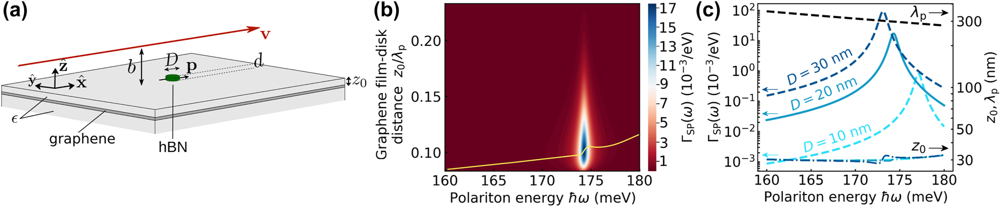
Free-electron excitation of graphene plasmons mediated by a hBN disk scatterer. (a) Geometry under consideration, comprising a graphene film and an hBN disk of diameter D and thickness d. The disk is directly deposited on the top dielectric layer of thickness z 0. The electron passes at a distance b above the disk. The dielectric substrate and coating layer have a permittivity ϵ. (b) Spectrally resolved probability of graphene-plasmon emission ΓSP(ω) under the conditions of (a) as a function of plasmon energy ℏω and coating-layer thickness z 0 for D = 20 nm, d = 1 nm, ϵ = 2, b = 10 nm, and v = 0.04 c. We set the graphene Fermi energy to E F = 1 eV. (c) Maximum ΓSP(ω) (left vertical scale, solid curve) and optimum coating thickness z 0 along with the SP wavelength λ p (right scale) as a function of emission frequency under the conditions of (b). In (c), we also show results for the maximum ΓSP(ω) with D = 10 nm and 30 nm (see labels).
The effective disk polarizability cannot be calculated by following the approach used above for a self-standing scatterer because the Green tensor diverges as the disk-surface separation is reduced. Instead, we use an analytical expression for the polarizability of a disk deposited on a homogeneous substrate obtained from an electrostatic modal expansion [86], and then introduce the effect of the graphene layer through an ad hoc Green tensor, as shown in Methods (Section 5.2). In addition, the surface reflection coefficient needs to be modified to account for the new layered structure. A Fabry–Perot-type of analysis readily leads to
where r
0 = (ϵ − 1)/(ϵ + 1) and
Finally, the SP emission probability differs for the geometry in Figure 2(a) relative to Figure 1(a). A calculation based on the absorption density within the graphene film yields the result (see Section 5.3 in Methods)
similar to Eq. (14) but with p z = 0 (i.e., the induced disk dipole is parallel to the surface) and a modified Green tensor
which reduces to Eq. (7) when setting ϵ = 1.
We now use Eq. (18) combined with Eq. (19) to calculate the surface-polariton emission probability in the configuration of Figure 2(a). Here, the induced dipole
In Figure 2(b), we plot the resulting probability ΓSP(ω) as a function of disk–2D-layer spacer z 0 and frequency around the upper hBN Reststrahlen band for a disk thickness d = 1 nm (corresponding to 3 monolayers) and diameter D = 20 nm ≫ d. This choice for the disk diameter is motivated to enable a dipolar resonance within that band and boost the polarizability. In agreement with Figure 1, coupling to graphene plasmons is also maximized for an optimum frequency-dependent value of z 0/λ p. However, we now observe a strong dependence of ΓSP(ω) on mode frequency, with a sharp increase at a specific spectral position that is controlled by the intrinsic diameter-dependent resonance of the disk [see Figure 2(b) for D = 20 nm and Figure 2(c) for D = 10, 10, and 30 nm; see also Supplementary Materials, Figure S3(a) for the disk resonance frequency]. This feature demonstrates that the coupling scheme here considered allows us to select the excitation frequency of narrowband plasmons in a region where they would otherwise be inaccessible via direct electron excitation. Interestingly, the optimum z 0/λ p ratio takes smaller values than in Figure 1, presumably as a result of the weak scattering strength of the hBN disk compared to a perfect scatterer (see Supplementary Materials, Figure S4). This hypothesis is consistent with the observation that the maximum ΓSP(ω) and the optimum z 0 are both increasing with disk diameter [see the probability curves for D = 10, 20, and 30 nm in Figure 2(c)].
3 Polaritonic Smith–Purcell emission
Smith–Purcell radiation emission [76] occurs when an e-beam is oriented parallel to a grating such that there is a coherent superposition in the far-field emission associated with periodic elements. A “simple Huygens construction” [76] shows that broadband light is emitted along wavelength-dependent directions satisfying the phase-matching relation cos θ
n
= nλ
0/a + c/v, where a is the period and θ
n
is the emission angle relative to the electron velocity vector
![Figure 3:
Polaritonic Smith–Purcell effect. (a) Scheme with the geometry under consideration, similar to Figure 1(a) but with a linear array of particles spaced by a period a along the direction of electron motion. The in-plane emission angle θ
n
is indicated for one of the orders n [see Eq. (20)]. (b) Probability of SPP emission ΓSP,n
(ω) for different orders n normalized per particle and divided by the self-standing-particle EELS probability ΓEELS(ω) [Eq. (16)] as a function of scaled array–surface distance z
0/λ
p for fixed frequency ω = 0.4 ω
D. We assume perfect scatterers, a Drude film like that in Figure 1, and parameters a/λ
p = 2, v = 2.2 v
0 ≈ 0.2 c/(ϵ + 1), and k
D
b = 0.1. The corresponding emission angles θ
n
are indicated in the inset (top-view scheme). (c, d) Ratio ΓSP,n=−4(ω)/ΓEELS(ω) as a function of either (c) a/λ
p and z
0/λ
p for v/v
0 = 2.2, or (d) a/λ
p and v/v
0 for z
0/λ
p = 0.6, with all other parameters the same as in (b). The right vertical scale in (d) shows v/c for ϵ = 1. White regions in (c, d) correspond to the condition that the n = −4 Smith–Purcell emission is kinematically forbidden. Probability minima contours are observed as light-blue regions in (d) and marked by solid and dashed curves corresponding to the conditions cos θ
n
= 1 and −1, respectively, for the values of n indicated by labels.](/document/doi/10.1515/nanoph-2024-0326/asset/graphic/j_nanoph-2024-0326_fig_003.jpg)
Polaritonic Smith–Purcell effect. (a) Scheme with the geometry under consideration, similar to Figure 1(a) but with a linear array of particles spaced by a period a along the direction of electron motion. The in-plane emission angle θ n is indicated for one of the orders n [see Eq. (20)]. (b) Probability of SPP emission ΓSP,n (ω) for different orders n normalized per particle and divided by the self-standing-particle EELS probability ΓEELS(ω) [Eq. (16)] as a function of scaled array–surface distance z 0/λ p for fixed frequency ω = 0.4 ω D. We assume perfect scatterers, a Drude film like that in Figure 1, and parameters a/λ p = 2, v = 2.2 v 0 ≈ 0.2 c/(ϵ + 1), and k D b = 0.1. The corresponding emission angles θ n are indicated in the inset (top-view scheme). (c, d) Ratio ΓSP,n=−4(ω)/ΓEELS(ω) as a function of either (c) a/λ p and z 0/λ p for v/v 0 = 2.2, or (d) a/λ p and v/v 0 for z 0/λ p = 0.6, with all other parameters the same as in (b). The right vertical scale in (d) shows v/c for ϵ = 1. White regions in (c, d) correspond to the condition that the n = −4 Smith–Purcell emission is kinematically forbidden. Probability minima contours are observed as light-blue regions in (d) and marked by solid and dashed curves corresponding to the conditions cos θ n = 1 and −1, respectively, for the values of n indicated by labels.
Incidentally, while n < 0 is required by the traditional version of this effect to obtain a real emission angle θ n for free photons, polaritonic emission with a positive n is also possible for electrons moving faster than the SP phase velocity (i.e., v > c λ p/λ 0) and λ p < a. Here, we consider parameters for which direct excitation of polaritons (coincident with n = 0 emission) is kinematically forbidden.
3.1 Electron interaction with a linear array of scatterers
To analyze polaritonic Smith–Purcell emission, we assume again low inelastic losses, so that SPs can propagate far from the interaction region, where the direct and surface-reflected electron fields are negligible at frequencies below the crossing of the electron line and the mode dispersion [see Figure 1(b)]. In those far surface regions, the polariton field is dominated by the contribution of the k
‖ = k
p pole in
with
for an individual dipole placed at the origin.
We now consider an infinite linear array of period a formed by dipolar scatterers at positions
with
At large transverse distances |y| from the array, we expect the potential to be dominated by SP components emanating from the k ‖ = k p pole in Eq. (9). Using the same PPA procedure that allowed us to perform the k y integral in Eq. (8a) and obtain Eq. (13), we transform Eq. (22) into
with
Periodicity also allows us to write the induced dipoles as p(ω) ei(ω/v)aj , where the dependence on the position of each particle j reduces to a phase factor. In the absence of interaction among particles, p(ω) would be given by Eqs. (6a) and (6b). However, particle–particle interaction may become relevant for strong scatterers and small separations, so we include it in our calculations by defining the effective polarizability of each particle in the array as in Eq. (6b) but with the Green tensor supplemented by the contribution of the direct and surface-reflected fields produced by the rest of the dipoles. This is calculated in Methods (see Section 5.4), and in what follows, we use Eq. (6b) combined with Eq. (29) to obtain α eff(ω) for particles in the array.
To obtain the number of SPs produced by the passage of the electron, we consider the power density transported by a mode characterized by an electrostatic electric field
for the number of emitted SPs normalized to the number of scatterers in the array. For a given set of geometrical parameters and frequency, Smith–Purcell emission is only allowed for orders n satisfying the condition −k p ≤ 2πn/a + ω/v ≤ k p. In addition, Eq. (24) suggests that the Smith–Purcell emission at a given order n is boosted when polaritons are emitted along the direction of the array (i.e., sin θ n = 0), as we corroborate below.
We consider an array of perfect scatterers like the one sketched in Figure 3(a) and evaluate ΓSP,n (ω) using Eq. (24) with p(ω) calculated from Eqs. (6a), (13) and (15). The latter involves s = xx and zz components evaluated from Eq. (29) (notice that the direct lattice sum does not contribute to the imaginary part of the Green tensor). An illustrative result is presented in Figure 3(b) for all allowed emission orders n, normalized to the perfect-scatterer EELS probability [Eq. (16)]. Like in the configuration studied in Figure 1 for an individual scatterer, we find again a maximum emission at an optimum array–surface separation z 0, which is roughly independent of the order n. In Figure 3(c), we show the dependence of ΓSP,n for the strongest allowed mode n = −4 as a function of lattice period a and surface–array distance z 0. We observe singularities in the probability at specific values of a corresponding to the onset of new emission orders n < −1 (see Supplementary Materials, Figure S5). Nevertheless, the optimum value of z 0 that maximizes the emission is roughly independent of a. Incidentally, n = −4 emission is kinematically forbidden in the white regions in Figure 3(c) and (d). For each emission order n, plasmonic Smith–Purcell emission can thus be finely tuned by playing with the electron velocity, the period, and the array–surface separation.
Interestingly, similar singularities of ΓSP,−4 as a function of period a and electron velocity v are present in Figure 3(d), corresponding to light-blue contours in the color plot. In particular, contours with a positive slope emerge from the condition θ n = π (i.e., anti-parallel emission relative to the electron velocity vector) for different orders n = −4, − 5, … (from left to right). The origin of these features is analogous to lattice resonances in particle arrays [87], emerging when the wavelength matches the lattice period, or equivalently, at the onset of every diffraction order. Ultimately, this is the result of the accumulation of in-phase fields emanating from the different particle dipoles in the array [88]. In our system, the array period is small compared with the light wavelength, so free light propagation cannot produce in-phase contributions. However, fields propagating as surface modes can be in phase when the polariton wavelength λ p is close to the period a. This translates into a divergent-like behavior of the lattice sum in Eq. (28) (see Supplementary Materials, Figure S5 for a plot of this sum), that in turn permeates the induced dipoles and the resulting emission probability in Eq. (24). Likewise, features in Figure 3(d) emerging as negative-slope contours also originate in lattice resonances for forward-propagating polaritons at θ n = 0 with n = 1, 2, … from left to right.
3.2 Smith–Purcell emission with an array of hBN nanodisks
In Figure 4, we consider a linear array of hBN nanodisks with similar substrate and size parameters as in Figure 2. For simplicity, we assume ϵ = 1 (this condition is nearly met by amorphous silica at the mid-infrared frequencies under consideration), so we can apply the above formalism and calculate the probability from Eq. (24) with
![Figure 4:
Smith–Purcell emission of surface-plasmon polaritons in grapheme. We consider a geometry similar to Figure 2(a) but with an array of hBN disks instead of just an individual particle and setting ϵ = 1 for simplicity [see inset in (b)]. (a) Emission probability per particle ΓSP,n
(ω) for different orders n and fixed energy ℏω = 174 meV (SP wavelength λ
p = 299 nm) as a function of z
0. We set the period to a = 2 λ
p = 598 nm, while the rest of the disk and substrate parameters are the same as in Figure 2. Emission angles θ
n
for the propagating orders n are indicated in the inset on a top view of the linear array (green circles). (b) Emission probability per particle for orders shown in (a) as a function of period a for z
0 = 40 nm and v = 0.04 c. The dashed-black line marks the value a = 598 nm used in panel (a). Each order n exhibits a vertical asymptote at a specific value of a, below which is not allowed. (c) Emission probability per particle for n = −4 as a function of a and v/c for z
0 = 40 nm, with all other parameters the same as in (b). The white region corresponds to conditions for which n = −4 Smith–Purcell emission is kinematically forbidden. The conditions cos θ
−4 = −1 and cos θ
−4 = 0 are indicated by dashed-blue and dashed-orange curves, respectively.](/document/doi/10.1515/nanoph-2024-0326/asset/graphic/j_nanoph-2024-0326_fig_004.jpg)
Smith–Purcell emission of surface-plasmon polaritons in grapheme. We consider a geometry similar to Figure 2(a) but with an array of hBN disks instead of just an individual particle and setting ϵ = 1 for simplicity [see inset in (b)]. (a) Emission probability per particle ΓSP,n (ω) for different orders n and fixed energy ℏω = 174 meV (SP wavelength λ p = 299 nm) as a function of z 0. We set the period to a = 2 λ p = 598 nm, while the rest of the disk and substrate parameters are the same as in Figure 2. Emission angles θ n for the propagating orders n are indicated in the inset on a top view of the linear array (green circles). (b) Emission probability per particle for orders shown in (a) as a function of period a for z 0 = 40 nm and v = 0.04 c. The dashed-black line marks the value a = 598 nm used in panel (a). Each order n exhibits a vertical asymptote at a specific value of a, below which is not allowed. (c) Emission probability per particle for n = −4 as a function of a and v/c for z 0 = 40 nm, with all other parameters the same as in (b). The white region corresponds to conditions for which n = −4 Smith–Purcell emission is kinematically forbidden. The conditions cos θ −4 = −1 and cos θ −4 = 0 are indicated by dashed-blue and dashed-orange curves, respectively.
Figure 4(a) shows the Smith–Purcell emission probability for all allowed orders. Similar to Figure 3, the Smith–Purcell emission probability is maximized at an optimum value of z 0 that is rather independent of n. This effect can be understood for the disks under consideration because there is no out-of-plane polarization (i.e., p z = 0), and therefore, the dependences of Eq. (24) on either n or z 0 can be factorized. Interestingly, the emission is strongest for n = −4 because the chosen lattice period a is close to the onset of this order [see Figure 4(b)], so the emission angle θ −4 = 162° is close to grazing [see inset of Figure 4(a)] and the probability scales as 1/sin θ −4 [see Eq. (24)]. In Figure 4(c), we show the onset of the n = −4 order by a dashed-blue curve corresponding to the condition θ −4 = 180°, which makes ΓSP,−4 divergent. Conversely, cos θ −4 = 90° and ΓSP,−4 vanishes along the dashed-orange line [see also Eq. (24)].
4 Conclusions
In summary, we show that free electrons can efficiently excite SPs assisted by the mediation of scatterers placed in the vicinity of a polariton-supporting surface. Our semi-analytical theory reveals that the emission probability is maximized for lossless resonant scatterers placed at an optimum distance from the surface. This method enables the emission of surface polaritons even if the electron cannot directly excite polaritons due to kinematic constraints. In particular, polaritons of relatively large phase velocity can still be excited by low-energy electrons. We further explore polaritonic Smith–Purcell emission mediated by linear arrays of scatterers under excitation by electrons moving parallel to the array. An optimum array–surface separation is also observed for maximum emission. Interestingly, lattice resonances emerge as singularities in the Smith–Purcell excitation probability, signaled by the onset of new emission orders when their corresponding polariton wavelengths match the period of the array. The fact that each Smith–Purcell emission order emits preferentially at a given angle that can be controlled by the properties of the surface, scatterer, and electron beam provides additional knobs to manipulate the excitation and steering of polaritons in extended surfaces without requiring their patterning. Similarly, the engineering of such arrays of scatterers (for example, through their individual polarizabilities or positions) could enable further control of the polaritonic fields, facilitating additional effects such as focusing of polaritons at designated positions through the use of aperiodic arrangements.
To excite strongly confined surface modes, we are interested in small scatterers compared to the light wavelength. This condition is hard to reconcile with the requirement of lossless particles, but some suitable choices can be found depending on the spectral range of interest. For example, we show that hBN disks are excellent resonant scatterers at mid-infrared frequencies, where they can sustain photon-polaritons with reasonably low material losses that are overshadowed by those associated with their coupling to SPs. Our results show that these particles can assist electron coupling to graphene plasmons under conditions for which direct coupling is kinematically forbidden. Mie modes in dielectric particles offer another possibility in a spectral range for which materials with a relatively high refractive index are available, such as silicon and germanium in the near-infrared. For visible frequencies, noble-metal nanoparticles can feature plasmonic resonances that only depend on morphology in the quasistatic limit (particle size much smaller than the light wavelength), so they can be made arbitrarily small down to a few nanometers (when nonlocal effects become relevant), although intrinsic losses in the material are substantial. We further envision arrays formed by optically trapped two-level atoms as an appealing approach to realize lossless resonant scatterers. Similar effects to the ones shown in this paper should be produced when using nondipolar, bulky scatterers, which can be of interest for experimental purposes. In that scenario, the assumed point-like approximation fails, so that full numerical simulations are required, which could be explored in future works.
The observation of Smith–Purcell radiation [76], [89] requires that electrons interact with many periods of a grating. State-of-the-art electron optics can produce energetic electrons collimated within a small angle (e.g.,
Unlike other methods of SP generation, the use of free electrons to excite SPs presents the advantage that no structuring of the surface is necessary, and although a spacer might be required to separate the scatterers from the SP-supporting interface, the latter still retains in-plane translational symmetry. Through the mediation of nanoparticles decorating the surface at an optimum distance, we show that SPs can be efficiently excited at places determined by the position of the particles and under conditions for which direct electron–polariton coupling is not possible when using low-energy electrons. In addition, resonant particles allow spectral selectivity of the generated polaritons, filtering specific frequencies from the broadband field provided by the moving electrons. For particle arrays, a directional emission of SPs is predicted, displaying interesting features associated with lattice resonances that deserve further exploration in future studies.
5 Methods
5.1 Optical response of the materials under consideration
The optical response of supported graphene is described through its surface conductivity in the Drude model [Eq. (10)], with ω
D = E
F/πℏ depending on the doping Fermi energy E
F. For silver, the permittivity can be well-approximated by a modified Drude model
An effective surface conductivity σ(ω) = iωd[1 − ϵ(ω)]/4π can be extracted from the material permittivity ϵ(ω) for a film of small thickness d compared with the polariton wavelength. We apply this approach to describe silver and hBN disks by setting ϵ(ω) to the respective permittivities of these materials (see above). For silver, this procedure leads to the Drude conductivity in Eq. (10) with
5.2 Effective polarizability of a thin disk near an embedded 2D layer
In the electrostatic limit, the in-plane polarizability of a thin disk of diameter D supported on a homogeneous substrate of permittivity ϵ can be expressed as [86]
in terms of contributions arising from different polaritonic eigenmodes j, which enter through their associated dipolar matrix elements ζ
j
and eigenvalues η
j
. Here,
The polarizability in Eq. (25a) assumes a thick substrate of permittivity ϵ. However, under the configuration considered in Figures 2 and 4, a 2D material layer [surface conductivity σ(ω)] is placed at a distance z
0 below the outer surface on which the disk is lying. This layer changes the polarizability to an effective value
with α ‖(ω) given by Eq. (25a) and
Compared to Eq. (7), this expression incorporates an overall factor 4ϵ/(ϵ + 1)2 arising from the forward and backward field transmission across the outer planar surface, as well as a denominator accounting for multiple scattering in the cavity defined by the surface and the 2D material. We use Eq. (25b) for the effective polarizability of the disk in Figures 2 and 4.
5.3 2D polariton emission probability by an induced dipole
We can obtain the SP emission probability from the energy absorbed by the 2D material in the configuration of Figure 1(a) under the assumption that the response is dominated by SPs. The energy absorbed by a material of permittivity ϵ
m
(ω) occupying a region V and exposed to an optical field E(r, ω) (in the frequency domain) is given by [77]
For the 2D material, we consider an arbitrarily small thickness d, which yields a high permittivity ϵ m (ω) = 1 + 4πiσ(ω)/ωd expressed in terms of the surface conductivity σ(ω). The normal electric field inside the material is therefore negligible because of the continuity of the normal displacement, while the parallel field created by the dipole at the surface plane is continuous and given by Eqs. (4a) and (4b) with z = −z 0. In the electrostatic limit, this field reduces to
Inserting this result into Eq. (26), carrying out the R integral analytically, and reducing the z integral to a factor d, we find
which, upon consideration of Eq. (9) and the dispersion relation
For the SP emission probability in the configuration of Figure 2(a), the in-plane field acting on the 2D layer takes a similar form as Eq. (27), but now setting p
z
= 0 for the disk, replacing
5.4 Dipole–dipole interaction in linear arrays
In a linear array, the dipole self-interaction needs to be supplemented by the contribution of the field induced by other dipoles. We thus redefine
For the surface-reflected components, we follow a procedure similar to the derivation of Eq. (22) and write
with k
nx
= ω/v + 2πn/a and
for the surface-reflected component of the Green tensor in the array, where
Funding source: Directorate-General XII, Science, Research, and Development
Award Identifier / Grant number: Horizon 2020 grant nos. FET-Proactive 101017720-eB
Funding source: H2020 European Research Council
Award Identifier / Grant number: Advanced Grant 101141220- QUEFES
Funding source: Ministerio de Ciencia e Innovación
Award Identifier / Grant number: PID2020-112625GB-I00 and Severo Ochoa CEX2019- 000
-
Research funding: This work was supported by the European Research Council (Advanced grant 101141220-QUEFES), the European Commission (Horizon 2020 grant nos. FET-Proactive 101017720-eBEAM and FET-Open 964591-SMART-electron), the Spanish MCINN (PID2020-112625GB-I00 and Severo Ochoa CEX2019-000910-S), the Catalan CERCA Program, Cellex and Mir-Puig Foundations.
-
Author contributions: All authors have accepted responsibility for the entire content of this manuscript and approved its submission.
-
Conflict of interest: Authors state no conflicts of interest.
-
Data availability: The data that support the findings of this study are available from the authors upon reasonable request.
References
[1] M. I. Stockman, “Nanoplasmonics: the physics behind the applications,” Phys. Today, vol. 64, pp. 39–44, 2011. https://doi.org/10.1063/1.3554315.Search in Google Scholar
[2] D. N. Basov, M. M. Fogler, and F. J. García de Abajo, “Polaritons in van der Waals materials,” Science, vol. 354, p. aag1992, 2016. https://doi.org/10.1126/science.aag1992.Search in Google Scholar PubMed
[3] R. A. Álvarez-Puebla, L. M. Liz-Marzán, and F. J. García de Abajo, “Light concentration at the nanometer scale,” J. Phys. Chem. Lett., vol. 1, pp. 2428–2434, 2010. https://doi.org/10.1021/jz100820m.Search in Google Scholar
[4] S. Dai, et al.., “Tunable phonon polaritons in atomically thin van der Waals crystals of boron nitride,” Science, vol. 343, pp. 1125–1129, 2014. https://doi.org/10.1126/science.1246833.Search in Google Scholar PubMed
[5] Z. M. Abd El-Fattah, et al.., “Plasmonics in atomically thin crystalline silver films,” ACS Nano, vol. 13, pp. 7771–7779, 2019. https://doi.org/10.1021/acsnano.9b01651.Search in Google Scholar PubMed
[6] P. A. Kossyrev, et al.., “Electric field tuning of plasmonic response of nanodot array in liquid crystal matrix,” Nano Lett., vol. 5, pp. 1978–1981, 2005. https://doi.org/10.1021/nl0513535.Search in Google Scholar PubMed
[7] L. Ju, et al.., “Graphene plasmonics for tunable terahertz metamaterials,” Nat. Nanotechnol., vol. 6, pp. 630–634, 2011. https://doi.org/10.1038/nnano.2011.146.Search in Google Scholar PubMed
[8] F. Yi, E. Shim, A. Y. Zhu, H. Zhu, J. C. Reed, and E. Cubukcu, “Voltage tuning of plasmonic absorbers by indium tin oxide,” Appl. Phys. Lett., vol. 102, 2013, Art. no. 221102. https://doi.org/10.1063/1.4809516.Search in Google Scholar
[9] Z. Fei, et al.., “Gate-tuning of graphene plasmons revealed by infrared nano-imaging,” Nature, vol. 487, pp. 82–85, 2012. https://doi.org/10.1038/nature11253.Search in Google Scholar PubMed
[10] H. Liu, Y. Liu, and D. Zhu, “Chemical doping of graphene,” J. Mater. Chem., vol. 21, pp. 3335–3345, 2011. https://doi.org/10.1039/c0jm02922j.Search in Google Scholar
[11] C. Bie, H. Yu, B. Cheng, W. Ho, J. Fan, and J. Yu, “Design, fabrication, and mechanism of nitrogen-doped graphene-based photocatalyst,” Adv. Mater., vol. 33, 2021, Art. no. 2003521. https://doi.org/10.1002/adma.202003521.Search in Google Scholar PubMed
[12] M. Wang, et al.., “Magnetic tuning of plasmonic excitation of gold nanorods,” J. Am. Chem. Soc., vol. 135, pp. 15302–15305, 2013. https://doi.org/10.1021/ja408289b.Search in Google Scholar PubMed
[13] G. X. Ni, et al.., “Ultrafast optical switching of infrared plasmon polaritons in high-mobility graphene,” Nat. Photonics, vol. 10, pp. 244–247, 2016. https://doi.org/10.1038/nphoton.2016.45.Search in Google Scholar
[14] M. M. Jadidi, et al.., “Nonlinear terahertz absorption of graphene plasmons,” Nano Lett., vol. 16, pp. 2734–2738, 2016. https://doi.org/10.1021/acs.nanolett.6b00405.Search in Google Scholar PubMed
[15] J. D. Cox and F. J. García de Abajo, “Nonlinear graphene nanoplasmonics,” Acc. Chem. Res., vol. 52, pp. 2536–2547, 2019. https://doi.org/10.1021/acs.accounts.9b00308.Search in Google Scholar PubMed
[16] E. J. C. Dias, R. Yu, and F. J. García de Abajo, “Thermal manipulation of plasmons in atomically thin films,” Light: Sci. Appl., vol. 9, p. 87, 2020. https://doi.org/10.1038/s41377-020-0322-z.Search in Google Scholar PubMed PubMed Central
[17] J. N. Anker, W. P. Hall, O. Lyandres, N. C. Shah, J. Zhao, and R. P. Van Duyne, “Biosensing with plasmonic nanosensors,” Nat. Mater., vol. 7, pp. 442–453, 2008. https://doi.org/10.1038/nmat2162.Search in Google Scholar PubMed
[18] A. G. Brolo, “Plasmonics for future biosensors,” Nat. Photonics, vol. 6, pp. 709–713, 2012. https://doi.org/10.1038/nphoton.2012.266.Search in Google Scholar
[19] X. Yang, et al.., “Nanomaterial-based plasmon-enhanced infrared spectroscopy,” Adv. Mater., vol. 30, 2018, Art. no. 1704896. https://doi.org/10.1002/adma.201704896.Search in Google Scholar PubMed
[20] N. Rohaizad, C. C. Mayorga-Martinez, M. Fojtu, N. M. Latiff, and M. Pumera, “Two-dimensional materials in biomedical, biosensing and sensing applications,” Chem. Soc. Rev., vol. 50, pp. 619–657, 2021. https://doi.org/10.1039/d0cs00150c.Search in Google Scholar PubMed
[21] Z. Yu, G. Veronis, S. Fan, and M. L. Brongersma, “Design of midinfrared photodetectors enhanced by surface plasmons on grating structures,” Appl. Phys. Lett., vol. 89, 2006, Art. no. 151116. https://doi.org/10.1063/1.2360896.Search in Google Scholar
[22] F. H. L. Koppens, T. Mueller, P. Avouris, A. C. Ferrari, M. S. Vitiello, and M. Polini, “Photodetectors based on graphene, other two-dimensional materials and hybrid systems,” Nat. Nanotechnol., vol. 9, pp. 780–793, 2014. https://doi.org/10.1038/nnano.2014.215.Search in Google Scholar PubMed
[23] S. Yuan, et al.., “Room temperature graphene mid-infrared bolometer with a broad operational wavelength range,” ACS Photonics, vol. 7, pp. 1206–1215, 2020. https://doi.org/10.1021/acsphotonics.0c00028.Search in Google Scholar
[24] H. A. Atwater and A. Polman, “Plasmonics for improved photovoltaic devices,” Nat. Mater., vol. 9, pp. 205–213, 2010. https://doi.org/10.1038/nmat2629.Search in Google Scholar PubMed
[25] N. W. Teng, S. S. Yang, and F. C. Chen, “Plasmonic-enhanced organic photovoltaic devices for low-power light applications,” IEEE J. Photovolt., vol. 8, pp. 752–756, 2018. https://doi.org/10.1109/jphotov.2018.2797975.Search in Google Scholar
[26] S. Palomba and L. Novotny, “Nonlinear excitation of surface plasmon polaritons by four-wave mixing,” Phys. Rev. Lett., vol. 101, 2008, Art. no. 056802. https://doi.org/10.1103/physrevlett.101.056802.Search in Google Scholar PubMed
[27] M. Kauranen and A. V. Zayats, “Nonlinear plasmonics,” Nat. Photonics, vol. 6, pp. 737–748, 2012. https://doi.org/10.1038/nphoton.2012.244.Search in Google Scholar
[28] N. C. Panoiu, W. E. I. Sha, D. Y. Lei, and G.-C. Li, “Nonlinear optics in plasmonic nanostructures,” J. Opt., vol. 20, 2018, Art. no. 083001. https://doi.org/10.1088/2040-8986/aac8ed.Search in Google Scholar
[29] F. Bonaccorso, Z. Sun, T. Hasan, and A. C. Ferrari, “Graphene photonics and optoelectronics,” Nat. Photonics, vol. 4, pp. 611–622, 2010. https://doi.org/10.1038/nphoton.2010.186.Search in Google Scholar
[30] F. J. García de Abajo, “Graphene plasmonics: challenges and opportunities,” ACS Photonics, vol. 1, pp. 135–152, 2014. https://doi.org/10.1021/ph400147y.Search in Google Scholar
[31] J. Zhang, X. Wei, I. D. Rukhlenko, H. T. Chen, and W. Zhu, “Electrically tunable metasurface with independent frequency and amplitude modulations,” ACS Photonics, vol. 7, pp. 265–271, 2020. https://doi.org/10.1021/acsphotonics.9b01532.Search in Google Scholar
[32] E. Kretschmann and H. Raether, “Radiative decay of non radiative surface plasmons excited by light,” Z. Naturforsch. A, vol. 23, pp. 2135–2136, 1968. https://doi.org/10.1515/zna-1968-1247.Search in Google Scholar
[33] R. Hillenbrand, B. Knoll, and F. Keilmann, “Pure optical contrast in scattering-type scanning near-field microscopy,” J. Microsc., vol. 202, pp. 77–83, 2001. https://doi.org/10.1046/j.1365-2818.2001.00794.x.Search in Google Scholar PubMed
[34] R. Desgarceaux, et al.., “High-resolution photonic force microscopy based on sharp nanofabricated tips,” Nano Lett., vol. 20, pp. 4249–4255, 2020. https://doi.org/10.1021/acs.nanolett.0c00729.Search in Google Scholar PubMed PubMed Central
[35] C. Chen and P. Berini, “Grating couplers for broadside input and output coupling of long-range surface plasmons,” Opt. Express, vol. 18, pp. 8006–8018, 2010. https://doi.org/10.1364/oe.18.008006.Search in Google Scholar PubMed
[36] P. Alonso-González, et al.., “Controlling graphene plasmons with resonant metal antennas and spatial conductivity patterns,” Science, vol. 344, pp. 1369–1373, 2014. https://doi.org/10.1126/science.1253202.Search in Google Scholar PubMed
[37] A. García-Etxarri, I. Romero, F. J. García de Abajo, R. Hillenbrand, and J. Aizpurua, “Influence of the tip in near-field imaging of nanoparticle plasmonic modes: weak and strong coupling regimes,” Phys. Rev. B, vol. 79, 2009, Art. no. 125439. https://doi.org/10.1103/physrevb.79.125439.Search in Google Scholar
[38] M. B. Raschke and C. Lienau, “Apertureless near-field optical microscopy: tip–sample coupling in elastic light scattering,” Appl. Phys. Lett., vol. 83, pp. 5089–5091, 2003. https://doi.org/10.1063/1.1632023.Search in Google Scholar
[39] E. J. C. Dias and F. J. García de Abajo, “Fundamental limits to the coupling between light and 2D polaritons,” ACS Nano, vol. 13, pp. 5184–5197, 2019. https://doi.org/10.1021/acsnano.8b09283.Search in Google Scholar PubMed
[40] E. J. C. Dias and F. J. García de Abajo, “Complete coupling of focused light to surface polaritons,” Optica, vol. 8, pp. 520–531, 2021. https://doi.org/10.1364/optica.416718.Search in Google Scholar
[41] F. J. García de Abajo, “Optical excitations in electron microscopy,” Rev. Mod. Phys., vol. 82, pp. 209–275, 2010. https://doi.org/10.1103/revmodphys.82.209.Search in Google Scholar
[42] C. J. Powell and J. B. Swan, “Origin of the characteristic electron energy losses in aluminum,” Phys. Rev., vol. 115, pp. 869–875, 1959. https://doi.org/10.1103/physrev.115.869.Search in Google Scholar
[43] R. B. Pettit, J. Silcox, and R. Vincent, “Measurement of surface-plasmon dispersion in oxidized aluminum films,” Phys. Rev. B, vol. 11, pp. 3116–3123, 1975. https://doi.org/10.1103/physrevb.11.3116.Search in Google Scholar
[44] O. L. Krivanek, et al.., “Vibrational spectroscopy in the electron microscope,” Nature, vol. 514, pp. 209–214, 2014. https://doi.org/10.1038/nature13870.Search in Google Scholar PubMed
[45] M. J. Lagos, A. Trügler, U. Hohenester, and P. E. Batson, “Mapping vibrational surface and bulk modes in a single nanocube,” Nature, vol. 543, pp. 529–532, 2017. https://doi.org/10.1038/nature21699.Search in Google Scholar PubMed
[46] F. S. Hage, et al.., “Nanoscale momentum-resolved vibrational spectroscopy,” Sci. Adv., vol. 4, 2018, Art. no. eaar7495. https://doi.org/10.1126/sciadv.aar7495.Search in Google Scholar PubMed PubMed Central
[47] M. J. Lagos and P. E. Batson, “Thermometry with subnanometer resolution in the electron microscope using the principle of detailed balancing,” Nano Lett., vol. 18, pp. 4556–4563, 2018. https://doi.org/10.1021/acs.nanolett.8b01791.Search in Google Scholar PubMed
[48] F. S. Hage, D. M. Kepaptsoglou, Q. M. Ramasse, and L. J. Allen, “Phonon spectroscopy at atomic resolution,” Phys. Rev. Lett., vol. 122, 2019, Art. no. 016103. https://doi.org/10.1103/physrevlett.122.016103.Search in Google Scholar
[49] J. A. Hachtel, et al.., “Identification of site-specific isotopic labels by vibrational spectroscopy in the electron microscope,” Science, vol. 363, pp. 525–528, 2019. https://doi.org/10.1126/science.aav5845.Search in Google Scholar PubMed
[50] F. S. Hage, G. Radtke, D. M. Kepaptsoglou, M. Lazzeri, and Q. M. Ramasse, “Single-atom vibrational spectroscopy in the scanning transmission electron microscope,” Science, vol. 367, pp. 1124–1127, 2020. https://doi.org/10.1126/science.aba1136.Search in Google Scholar PubMed
[51] X. Yan, et al.., “Single-defect phonons imaged by electron microscopy,” Nature, vol. 589, pp. 65–69, 2021. https://doi.org/10.1038/s41586-020-03049-y.Search in Google Scholar PubMed
[52] K. Wang, et al.., “Coherent interaction between free electrons and a photonic cavity,” Nature, vol. 582, pp. 50–54, 2020. https://doi.org/10.1038/s41586-020-2321-x.Search in Google Scholar PubMed
[53] E. Pomarico, et al.., “meV resolution in laser-assisted energy-filtered transmission electron microscopy,” ACS Photonics, vol. 5, pp. 759–764, 2018. https://doi.org/10.1021/acsphotonics.7b01393.Search in Google Scholar
[54] M. Kociak and O. Stéphan, “Mapping plasmons at the nanometer scale in an electron microscope,” Chem. Soc. Rev., vol. 43, pp. 3865–3883, 2014. https://doi.org/10.1039/c3cs60478k.Search in Google Scholar PubMed
[55] B. Barwick, D. J. Flannigan, and A. H. Zewail, “Photon-induced near-field electron microscopy,” Nature, vol. 462, pp. 902–906, 2009. https://doi.org/10.1038/nature08662.Search in Google Scholar PubMed
[56] S. T. Park, M. Lin, and A. H. Zewail, “Photon-induced near-field electron microscopy (PINEM): theoretical and experimental,” New J. Phys., vol. 12, 2010, Art. no. 123028. https://doi.org/10.1088/1367-2630/12/12/123028.Search in Google Scholar
[57] S. T. Park and A. H. Zewail, “Relativistic effects in photon-induced near field electron microscopy,” J. Phys. Chem. A, vol. 116, pp. 11128–11133, 2012. https://doi.org/10.1021/jp304534n.Search in Google Scholar PubMed
[58] A. Feist, K. E. Echternkamp, J. Schauss, S. V. Yalunin, S. Schäfer, and C. Ropers, “Quantum coherent optical phase modulation in an ultrafast transmission electron microscope,” Nature, vol. 521, pp. 200–203, 2015. https://doi.org/10.1038/nature14463.Search in Google Scholar PubMed
[59] K. E. Priebe, et al.., “Attosecond electron pulse trains and quantum state reconstruction in ultrafast transmission electron microscopy,” Nat. Photonics, vol. 11, pp. 793–797, 2017. https://doi.org/10.1038/s41566-017-0045-8.Search in Google Scholar
[60] Y. Morimoto and P. Baum, “Attosecond control of electron beams at dielectric and absorbing membranes,” Phys. Rev. A, vol. 97, 2018, Art. no. 033815. https://doi.org/10.1103/physreva.97.033815.Search in Google Scholar
[61] Y. Morimoto and P. Baum, “Diffraction and microscopy with attosecond electron pulse trains,” Nat. Phys., vol. 14, pp. 252–256, 2018. https://doi.org/10.1038/s41567-017-0007-6.Search in Google Scholar
[62] M. Kozák, et al.., “Optical gating and streaking of free electrons with sub-optical cycle precision,” Nat. Commun., vol. 8, 2017, Art. no. 14342. https://doi.org/10.1038/ncomms14342.Search in Google Scholar PubMed PubMed Central
[63] A. Feist, S. V. Yalunin, S. Schäfer, and C. Ropers, “High-purity free-electron momentum states prepared by three-dimensional optical phase modulation,” Phys. Rev. Res., vol. 2, 2020, Art. no. 043227. https://doi.org/10.1103/physrevresearch.2.043227.Search in Google Scholar
[64] O. Kfir, et al.., “Controlling free electrons with optical whispering-gallery modes,” Nature, vol. 582, pp. 46–49, 2020. https://doi.org/10.1038/s41586-020-2320-y.Search in Google Scholar PubMed
[65] I. Madan, G. M. Vanacore, S. Gargiulo, T. LaGrange, and F. Carbone, “The quantum future of microscopy: wave function engineering of electrons, ions, and nuclei,” Appl. Phys. Lett., vol. 116, 2020, Art. no. 230502. https://doi.org/10.1063/1.5143008.Search in Google Scholar
[66] G. M. Vanacore, I. Madan, and F. Carbone, “Spatio-temporal shaping of a free-electron wave function via coherent light-electron interaction,” Riv. Nuovo Cimento, vol. 43, pp. 567–597, 2020. https://doi.org/10.1007/s40766-020-00012-5.Search in Google Scholar
[67] R. Dahan, et al.., “Resonant phase-matching between a light wave and a free-electron wavefunction,” Nat. Phys., vol. 16, pp. 1123–1131, 2020. https://doi.org/10.1038/s41567-020-01042-w.Search in Google Scholar
[68] J.-W. Henke, et al.., “Integrated photonics enables continuous-beam electron phase modulation,” Nature, vol. 600, pp. 653–658, 2021. https://doi.org/10.1038/s41586-021-04197-5.Search in Google Scholar PubMed PubMed Central
[69] G. M. Vanacore, et al.., “Ultrafast generation and control of an electron vortex beam via chiral plasmonic near fields,” Nat. Mater., vol. 18, pp. 573–579, 2019. https://doi.org/10.1038/s41563-019-0336-1.Search in Google Scholar PubMed
[70] J. Schefold, et al.., “Spatial resolution of coherent cathodoluminescence super-resolution microscopy,” ACS Photonics, vol. 4, pp. 1067–1072, 2019. https://doi.org/10.1021/acsphotonics.9b00164.Search in Google Scholar PubMed PubMed Central
[71] A. Polman, M. Kociak, and F. J. García de Abajo, “Electron-beam spectroscopy for nanophotonics,” Nat. Mater., vol. 18, pp. 1158–1171, 2019. https://doi.org/10.1038/s41563-019-0409-1.Search in Google Scholar PubMed
[72] S. V. Yalunin, A. Feist, and C. Ropers, “Tailored high-contrast attosecond electron pulses for coherent excitation and scattering,” Phys. Rev. Res., vol. 3, 2021, Art. no. L032036. https://doi.org/10.1103/physrevresearch.3.l032036.Search in Google Scholar
[73] F. J. García de Abajo and C. Ropers, “Spatiotemporal electron beam focusing through parallel interactions with shaped optical fields,” Phys. Rev. Lett., vol. 130, 2023, Art. no. 246901. https://doi.org/10.1103/physrevlett.130.246901.Search in Google Scholar PubMed
[74] A. Howie, “Electrons and photons: exploiting the connection,” Inst. Phys. Conf. Ser., vol. 161, pp. 311–314, 1999.Search in Google Scholar
[75] F. J. García de Abajo and M. Kociak, “Electron energy-gain spectroscopy,” New J. Phys., vol. 10, 2008, Art. no. 073035. https://doi.org/10.1088/1367-2630/10/7/073035.Search in Google Scholar
[76] S. J. Smith and E. M. Purcell, “Visible light from localized surface charges moving across a grating,” Phys. Rev., vol. 92, p. 1069, 1953. https://doi.org/10.1103/physrev.92.1069.Search in Google Scholar
[77] J. D. Jackson, Classical Electrodynamics, New York, Wiley, 1999.Search in Google Scholar
[78] P. A. D. Gonçalves and N. M. R. Peres, An Introduction to Graphene Plasmonics, Singapore, World Scientific, 2016.10.1142/9948Search in Google Scholar
[79] M. Jablan, H. Buljan, and M. Soljačić, “Plasmonics in graphene at infrared frequencies,” Phys. Rev. B, vol. 80, 2009, Art. no. 245435. https://doi.org/10.1103/physrevb.80.245435.Search in Google Scholar
[80] A. N. Grigorenko, M. Polini, and K. S. Novoselov, “Graphene plasmonics,” Nat. Photonics, vol. 6, pp. 749–758, 2012. https://doi.org/10.1038/nphoton.2012.262.Search in Google Scholar
[81] G. X. Ni, et al.., “Fundamental limits to graphene plasmonics,” Nature, vol. 557, pp. 530–533, 2018. https://doi.org/10.1038/s41586-018-0136-9.Search in Google Scholar PubMed
[82] P. B. Johnson and R. W. Christy, “Optical constants of the noble metals,” Phys. Rev. B, vol. 6, pp. 4370–4379, 1972. https://doi.org/10.1103/physrevb.6.4370.Search in Google Scholar
[83] I. S. Gradshteyn and I. M. Ryzhik, Table of Integrals, Series, and Products, London, Academic Press, 2007.Search in Google Scholar
[84] L. A. Blanco and F. J. García de Abajo, “Spontaneous light emission in complex nanostructures,” Phys. Rev. B, vol. 69, 2004, Art. no. 205414. https://doi.org/10.1103/physrevb.69.205414.Search in Google Scholar
[85] F. J. García de Abajo and V. Di Giulio, “Optical excitations with electron beams: challenges and opportunities,” ACS Photonics, vol. 8, pp. 945–974, 2021. https://doi.org/10.1021/acsphotonics.0c01950.Search in Google Scholar PubMed PubMed Central
[86] R. Yu, J. D. Cox, J. R. M. Saavedra, and F. J. García de Abajo, “Analytical modeling of graphene plasmons,” ACS Photonics, vol. 4, pp. 3106–3114, 2017. https://doi.org/10.1021/acsphotonics.7b00740.Search in Google Scholar
[87] F. J. García de Abajo, “Colloquium: light scattering by particle and hole arrays,” Rev. Mod. Phys., vol. 79, pp. 1267–1290, 2007. https://doi.org/10.1103/revmodphys.79.1267.Search in Google Scholar
[88] L. Rayleigh, “Note on the remarkable case of diffraction spectra described by Prof. Wood,” Philos. Mag., vol. 14, pp. 60–65, 1907. https://doi.org/10.1080/14786440709463661.Search in Google Scholar
[89] R. Remez, et al.., “Observing the quantum wave nature of free electrons through spontaneous emission,” Phys. Rev. Lett., vol. 123, 2019, Art. no. 060401. https://doi.org/10.1103/physrevlett.123.060401.Search in Google Scholar
[90] G. Guzzinati, A. Beche, H. Lourenço-Martins, J. Martin, M. Kociak, and J. Verbeeck, “Probing the symmetry of the potential of localized surface plasmon resonances with phase-shaped electron beams,” Nat. Commun., vol. 8, 2017, Art. no. 14999. https://doi.org/10.1038/ncomms14999.Search in Google Scholar PubMed PubMed Central
[91] R. Yu, L. M. Liz-Marzán, and F. J. García de Abajo, “Universal analytical modeling of plasmonic nanoparticles,” Chem. Soc. Rev., vol. 46, pp. 6710–6724, 2017. https://doi.org/10.1039/c6cs00919k.Search in Google Scholar PubMed
[92] J. D. Caldwell, et al.., “Sub-diffractional volume-confined polaritons in the natural hyperbolic material hexagonal boron nitride,” Nat. Commun., vol. 5, p. 5221, 2014. https://doi.org/10.1038/ncomms6221.Search in Google Scholar PubMed
Supplementary Material
This article contains supplementary material (https://doi.org/10.1515/nanoph-2024-0326).
© 2024 the author(s), published by De Gruyter, Berlin/Boston
This work is licensed under the Creative Commons Attribution 4.0 International License.
Articles in the same Issue
- Frontmatter
- Editorial
- Current trends in nanophotonics
- Review
- Applications of surface enhanced Raman scattering (SERS) spectroscopy for detection of nucleic acids
- Research Articles
- Design of optical Kerr effect in multilayer hyperbolic metamaterials
- A tiny Drude scatterer can accurately model a coherent emitter in nanophotonics
- Strong coupling spontaneous emission interference near a graphene nanodisk
- Long-range molecular energy transfer mediated by strong coupling to plasmonic topological edge states
- Thermal radiation forces on planar structures with asymmetric optical response
- Molecular surface coverage standards by reference-free GIXRF supporting SERS and SEIRA substrate benchmarking
- Effect of magnesium doping on NiO hole injection layer in quantum dot light-emitting diodes
- Anomalous reflection for highly efficient subwavelength light concentration and extraction with photonic funnels
- Nanometric probing with a femtosecond, intra-cavity standing wave
- Considerations for electromagnetic simulations for a quantitative correlation of optical spectroscopy and electron tomography of plasmonic nanoparticles
- Free-electron coupling to surface polaritons mediated by small scatterers