Fine structures of valley-polarized excitonic states in monolayer transitional metal dichalcogenides
-
Zhipeng Li
 ,
Tianmeng Wang
,
Tianmeng Wang


Abstract
Monolayer transitional metal dichalcogenides (TMDCs), a new class of atomically thin semiconductor, respond to optical excitation strongly with robust excitons, which stem from the reduced screening in two dimensions. These excitons also possess a new quantum degree of freedom known as valley spin, which has inspired the field of valleytronics. The strongly enhanced Coulomb interaction allows the exciton to bind with other particles to form new excitonic states. However, despite the discovery of trions, most of the excitonic states in monolayer TMDCs remain elusive until recently, when new light was shed into the fascinating excitonic fine structures with drastically improved sample quality through boron nitride encapsulation. Here, we review the latest research progress on fine structures of excitonic states in monolayer TMDCs, with a focus on tungsten-based TMDCs and related alloy. Many of the new excitonic complexes inherit the valley degree of freedom, and the valley-polarized dark excitonic states are of particular interest because of their long lifetime and possible long valley coherence time. The capability of resolving the excitonic fine structures also enables the investigation of exciton–phonon interactions. The knowledge of the interlayer between excitons and other particles not only advances our understanding of many-body effects in the monolayer TMDCs but also provides guidance on future applications based on TMDCs.
1 Introduction
Since the discovery of graphene from 2004 [1], [2], [3], two-dimensional materials (2D materials) have drawn intense attention in the research communities of physics, chemistry, material science, and engineering worldwide [4], [5], [6], [7], [8], [9], [10], [11], [12], [13]. Among them, transitional metal dichalcogenides (TMDCs) represent a new class of atomically thin semiconductor that host excitons with large binding energy due to enhanced Coulomb interaction in 2D. These excitons also possess valley contrasting properties, which stem from the combined effects of threefold rotation symmetry and inversion symmetry breaking. However, the lifetime of the excitons is typically short, rendering it difficult to realize valleytronics applications. Because the Coulomb interaction in confined 2D space is strong, is it possible for the exciton to bind with other particles to form new excitonic particles that are both valley-polarized and long-lived? How would the exciton–phonon interaction or other many-body physics affect the new excitonic states? These questions were challenging to address, mostly due to elusive spectra signatures limited by the quality of TMDC devices.
Notably, with the improvement of crystal growth [14], [15], [16], [17], [18], [19] and fabrication technique, especially the encapsulation of high-quality hexagonal boron nitride (h-BN) flakes [20], [21], [22], [23], [24], high-quality TMDCs devices have been shown to produce rich optical spectroscopy features that are associated with new excitonic complexes. In particular, tungsten-based TMDCs such as tungsten diselenide (WSe2) and tungsten disulfide (WS2) possess the unique band structure that hosts spin-forbidden dark exciton, which significantly enriches the library of the excitonic quasi-particles. In this article, we review the advances in the understanding of the emerging fine structures of excitonic states in TMDC monolayers, mainly taking WSe2 as the prototypical example: (i) the resolution of biexciton puzzle by identifying the charge-neutral biexciton and trion–exciton complexes (i.e., charged biexciton) [25], [26], [27], [28]; (ii) the verification of the dark exciton and dark trions through the gate voltage–dependent magneto-photoluminescence (PL) and Fourier plane imaging [29], [30], [31], [32]; (iii) the exciton–phonon interaction including the chiral phonon replica (E″ chiral phonon at Г point) of the spin-forbidden dark exciton replica [33], [34], momentum-dark intervalley exciton brightened by the chiral K phonon (E′ chiral phonon at K point) [35], [36], [37], [38], and the interlayer exciton–phonon coupling in the van der Waals (vdW) heterostructure of monolayer TMDC or alloy (WS0.6Se1.4) shown in the emerging Raman modes [22], [23], [39], [40]. Improved understanding of the excitonic fine structures in monolayer TMDCs and related alloy will allow us to explore valley-polarized excitonic complexes with long lifetime for valleytronics, to search for excitonic quasi-particle with long valley coherence, and to manipulate the valley spin through interactions such as phonon-exciton interaction. These efforts will greatly advance our understanding of the unique many-body physics in TMDCs and open the door to the novel quantum optoelectronics.
In the review, we only focus on the many-particle excitonic complexes that are not related to defects. For defect-related excitonic physics in monolayer TMDCs, we refer the interested readers to the recent reviews [4], [41].
2 Excitonic states in 2D TMDCs
Transitional metal dichalcogenides have an indirect-to-direct bandgap transition from bulk to single layer [42], [43]. The large spin-orbit coupling (SOC) leads to the splitting both in the valence and conduction bands with the splitting energies of ~300 to 400 and ~20 to 40 meV, respectively (Figure 1A) [48], [49], [50], [51]. Because of the inversion symmetry breaking and threefold rotation symmetry, the excitons in monolayer TMDCs are endowed with the valley degree of freedom, which behaves like a pseudospin [44], [45], [46], [52], [53], [54], [55], [56], [57], [58]. The valley degree of freedom can be accessed selectively through the circularly polarized light, that is, σ+ polarized light to selectively excite the K valley, whereas σ− polarized light to excite the K′ valley, which opens up the fascinating field of valleytronics [46], [53], [59], [60], [61], [62], [63], [64], [65], [66]. Meanwhile, despite the atomically thin structure, most of the monolayer TMDCs possess strong light–matter interaction. For instance, the monolayer MoS2 has ~10% resonant absorption of light (660 nm for A exciton and 615 nm for B exciton) [67]. With the reduced screening effect, the greatly enhanced Coulomb interaction between excited electron and hole results in the formation of extensively studied excitonic complexes [68], [69], [70], [71], such as bright exciton [42], [72], [73], dark exciton [31], [32], [74], [75], [76], [77], [78], and intravalley and intervalley trions [79], [80], [81], as well as positive trion [73], [82], with binding energy orders of magnitude larger than the counterpart in conventional semiconductor such as gallium arsenide [57], [63], [68], [83], [84], [85], [86] (Figure 1B–F).
![Figure 1: Excitonic states in 2D tungsten-based TMDC monolayer.(A) Valley-dependent optical selection rules for interband transitions in 2D monolayer tungsten-based TMDCs. Both the conduction and valence bands are spin-split due to the strong SOC, resulting in the spin-valley locking. σ+ polarized light only couples to the K valley, whereas σ− polarized light only couples to the K′ valley. Blue and red stand for spin up and spin down. (B–F) Excitonic configurations of the bright exciton (X0),$({{\rm{X}}_0}),$ dark exciton (XD),$({{\rm{X}}_{\rm{D}}}),$ intervalley negative trion (X1−),$({\rm{X}}_1^ - ),$ intravalley negative trion (X2−),$({\rm{X}}_2^ - ),$ and positive trion (X+), respectively. The z-component of the total angular momentum for each band, with the Berry phase contribution considered, is labeled in panel B [44], [45], [46], [47].](/document/doi/10.1515/nanoph-2020-0054/asset/graphic/j_nanoph-2020-0054_fig_001.jpg)
Excitonic states in 2D tungsten-based TMDC monolayer.
(A) Valley-dependent optical selection rules for interband transitions in 2D monolayer tungsten-based TMDCs. Both the conduction and valence bands are spin-split due to the strong SOC, resulting in the spin-valley locking. σ+ polarized light only couples to the K valley, whereas σ− polarized light only couples to the K′ valley. Blue and red stand for spin up and spin down. (B–F) Excitonic configurations of the bright exciton
Boron nitride encapsulation has been recently shown to significantly improve the TMDC device quality, which is evidenced by the PL spectra width [87], [88], [89], [90] and associated optical spectra. With the significant improvement of the quality of TMDC bulk crystal growth and the optimization of the device fabrication, especially with the high-quality h-BN encapsulation to isolate the monolayer TMDCs from dielectric environment (Figure 2A, B), the PL width of the exciton peak can be reduced to ~2 meV, limited by the intrinsic recombination [87], [88], [89], [90]. As a result, researchers are able to explore the intrinsic nature of the different excitonic states with the application of different tuning knobs, including electrostatic gating, magneto-PL, polarization, time-resolved PL (TRPL), and so on. Recently, it has been demonstrated that many novel excitonic states will emerge locating both in the hole-doping and electron-doping regimes in h-BN–encapsulated TMDC monolayer. Taking h-BN/WSe2/h-BN structure as an example (Figure 2C), in addition to the well-established bright exciton
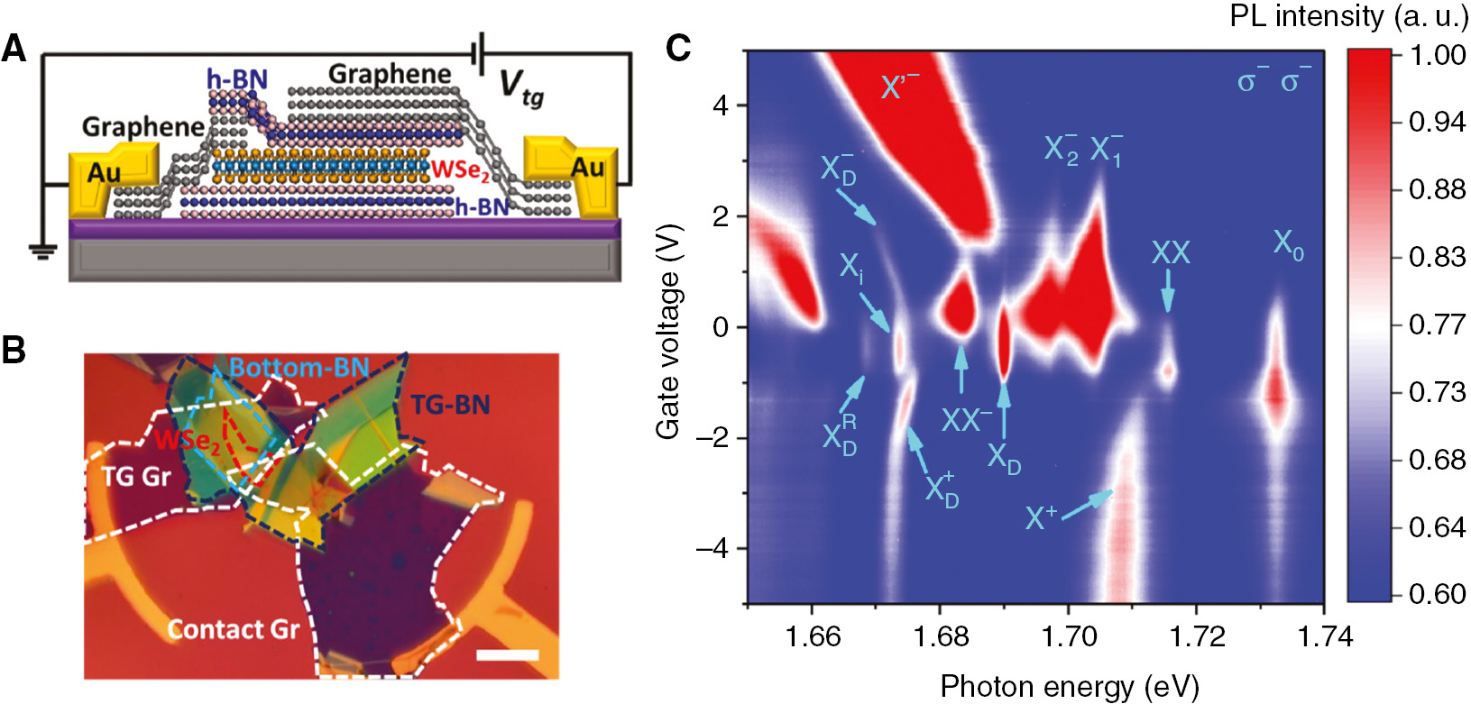
Gate voltage–dependent PL spectra of h-BN sandwiched monolayer WSe2.
(A) Schematic representing the h-BN sandwiched monolayer WSe2 device with a top gate. (B) A representative optical image of a top-gated WSe2 device, in which different flakes are highlighted by different-color dashed lines. (C) Electrostatic doping–dependent color plot of the PL spectra of monolayer WSe2 at low temperature (4.2 K). Owing to the efficient gate tunability, besides the bright exciton
3 Biexciton and trion–exciton complexes
The strong Coulomb interaction in monolayer TMDCs would give rise to strong exciton–exciton interaction, and we might expect the easy formation of biexciton. Although the biexciton was experimentally demonstrated as early as 2015, however, the theoretical calculations and experimental extracted value of the binding energy of biexciton remain discrepant, calling for unambiguous identification and understanding of the biexciton in TMDCs.
In 2015, You et al. [93] introduced the fluence-dependent PL study and TRPL to demonstrate the presence of a four-body biexciton state in monolayer WSe2. They found that under pulsed excitation an emerging state exhibits a superlinear power dependence with the power law of 1.39, which is distinctively different from other excitonic states with linear power dependence (Figure 3A, B). They ascribe this state to be the biexciton state. The TRPL results further indicate that the biexciton has the similar lifetime as the exciton and trion, in contrast to the long decay time of defect states (Figure 3C). The experimentally extracted binding energy is 52 meV, which is significantly larger than the theoretical prediction of ~20 meV. Many other research groups also report similar results both from monolayer WS2 and WSe2 [28], [94], [95], [96], [97], [98], [99], [100], [101]. However, these results are based on either the devices without gate tunability or the devices with relatively inferior spectral quality, which prevents them from exploring the intrinsic property of biexciton. Yong et al. [102] introduce the pump-probe technique to demonstrate that the driving optical field can couple a hierarchy of excitonic states, and the many-body intervalley biexciton state plays a dominant role in the optical Stark effect in monolayer MoSe2. They determine a binding energy of 21 meV for the intervalley biexciton and a transition dipole moment of 9.3 debyes for the exciton–biexciton transition (Figure 4A, B). In addition, Steinhoff et al. [104] and Hao et al. [103] utilize both the polarization-resolved 2D coherent spectroscopy on monolayer MoSe2 and ultrafast pump-probe measurement on single-layer WSe2 to reveal the high-order biexciton fine structures (“bright–bright” configuration) (Figure 4C–E). The biexcitons in MoSe2 and WSe2 both locate between the exciton and trion with the binding energy of around 20 meV, which is very close to the theoretical prediction [84], [85], [105], [106], [107]. Hence, which one is the real biexciton? What is the binding energy of the biexciton? This is the biexciton puzzle in the research community of 2D materials.
![Figure 3: Excitonic states in monolayer WSe2.(A) Photoluminescence spectra for different excitation fluences of 0.8 and 12 μJ·cm−2 at 50 K. (B) Logarithmic plot of the XX PL intensity as a function of the PL intensity of exciton. The red line is a power-law fit: IXX∝IXα, with α=1.39. The linear relation is shown for a comparison (dashed black line). (C) Time-resolved PL traces for X, X−, XX, P1, and P2 species and the instrument response function. The decay of XX is similar to that of X and X−, but it is distinctively different from defect-related P1 and P2, which have decay times >100 ps. The emission lifetimes are 14, 25, and 31 ps for X, X−, and XX, respectively, with uncertainties of ±5 ps. (A–C) Adapted from You et al. [93].](/document/doi/10.1515/nanoph-2020-0054/asset/graphic/j_nanoph-2020-0054_fig_003.jpg)
Excitonic states in monolayer WSe2.
(A) Photoluminescence spectra for different excitation fluences of 0.8 and 12 μJ·cm−2 at 50 K. (B) Logarithmic plot of the XX PL intensity as a function of the PL intensity of exciton. The red line is a power-law fit: IXX∝IXα, with α=1.39. The linear relation is shown for a comparison (dashed black line). (C) Time-resolved PL traces for X, X−, XX, P1, and P2 species and the instrument response function. The decay of XX is similar to that of X and X−, but it is distinctively different from defect-related P1 and P2, which have decay times >100 ps. The emission lifetimes are 14, 25, and 31 ps for X, X−, and XX, respectively, with uncertainties of ±5 ps. (A–C) Adapted from You et al. [93].
![Figure 4: Excitonic states in 2D TMDC monolayer.(A) Transient reflection spectra at τ=0 ps with different detuning energies. (B) Schematic of the effective coupling between different states upon σ+-pump radiation. Adapted from Yong et al. [102]. (C) Normalized 2D amplitude spectrum obtained using cross-circular polarization of the first/third fields (σ+) and second/signal fields (σ−). The XX is associated with the neutral bound biexciton, whereas the TXb and XTb are associated with the charged bound biexciton. Adapted from Hao et al. [103]. (D) Line cut at the excitation energy of ~1.648 eV from (C). Peaks XTb, XX, and X are indicated by the shaded regions with the fitting from Gaussian functions. Adapted from Hao et al. [103]. (E) Differential absorption of WSe2 pumped at the red wing of its neutral exciton resonance in a pump-probe experiment with cross-polarized (left panel) and cocircularly polarized (right panel) pump and probe pulses. Adapted from Steinhoff et al. [104].](/document/doi/10.1515/nanoph-2020-0054/asset/graphic/j_nanoph-2020-0054_fig_004.jpg)
Excitonic states in 2D TMDC monolayer.
(A) Transient reflection spectra at τ=0 ps with different detuning energies. (B) Schematic of the effective coupling between different states upon σ+-pump radiation. Adapted from Yong et al. [102]. (C) Normalized 2D amplitude spectrum obtained using cross-circular polarization of the first/third fields (σ+) and second/signal fields (σ−). The XX is associated with the neutral bound biexciton, whereas the TXb and XTb are associated with the charged bound biexciton. Adapted from Hao et al. [103]. (D) Line cut at the excitation energy of ~1.648 eV from (C). Peaks XTb, XX, and X are indicated by the shaded regions with the fitting from Gaussian functions. Adapted from Hao et al. [103]. (E) Differential absorption of WSe2 pumped at the red wing of its neutral exciton resonance in a pump-probe experiment with cross-polarized (left panel) and cocircularly polarized (right panel) pump and probe pulses. Adapted from Steinhoff et al. [104].
Li et al. [25], along with Ye et al. [28], Chen et al. [27], and Barbone et al. [26], independently report the identification of the neutral biexciton and trion–exciton complexes (or equivalently, negatively charged biexciton) in an h-BN–encapsulated monolayer WSe2 device. The authors demonstrate the superlinear fluence dependence (nearly quadratic power law) for two new excitonic states, XX and XX−, whereas the bright exciton shows an almost linear behavior. The XX locates between the exciton and the trions with the binding energy of ~17 meV, whereas the XX− lies on the low energy side of the dark exciton with the binding energy of ~49 meV, where the binding energy of XX is in excellent agreement with the theoretical prediction of biexciton binding energy, and the binding energy of XX− is consistent with the result of You et al. [93]. They further employ the efficient electrostatic gating from hole-doping to electron-doping to identify the nature of XX and XX− (Figure 2C). The XX only brightens up at the charge-neutral region, similar to the dark exciton. However, the XX− emerges at the slight electron-doping region, and the intensity quickly diminishes with the increase of the electron-doping. Considering the doping dependence and the fluence dependence of the PL, the XX and XX− are assigned to be charge-neutral biexciton and electron-bound biexciton, respectively. Meanwhile, the valley polarization of the XX and XX− is higher than that of the bright exciton, which indicates that they are both composed of a bright exciton. Because the XX− is a five-particle complex, considering the valley polarization and Pauli exclusion, the lowest energy configuration for XX− can only be the one shown in the left panel of Figure 5D, which can be viewed as a biexciton bound to a free electron or, equivalently, an intravalley trion bound to a dark exciton. Another interesting observation is that, in contrast to the bright exciton, the PL intensity of XX and XX− presents an inverse circular polarization under magnetic field, in which the high energy peak has more intense PL intensity than the low energy peak (Figure 5A). This observation is in agreement with the calculated total g factor (contributions from all the constituent particles) of the XX and XX− with the positive value of 4 and 6, respectively. Therefore, the configuration of the biexciton is also deduced as the one shown in the right panel of Figure 5D, taking into account the valley polarization and the inverted PL intensity behavior, which consists of a bright exciton and a dark exciton. Due to the long lifetime of the dark exciton (~hundreds of picoseconds), the bright exciton has high probability to bind with the high density of dark excitons to form the “bright-dark” biexciton, instead of the “bright–bright” biexciton, even at very low excitation power (~μW/μm−2). Finally, the authors obtain the magneto-PL spectra and extract the spectral g factor for the XX and XX− with the value of −4.03 and −5.33 (Figure 5B, C), respectively, which is in excellent agreement with the theoretical expectation from the valley-Zeeman effect [108], [109], [110], [111] (Figure 5B, C). Additionally, the dark exciton exhibits a unique X-pattern, originating from the out-of-plane radiation dipole. The g factor of the dark exciton (–9.75) is significantly larger than the bright exciton, which is consistent with the previous report [76].
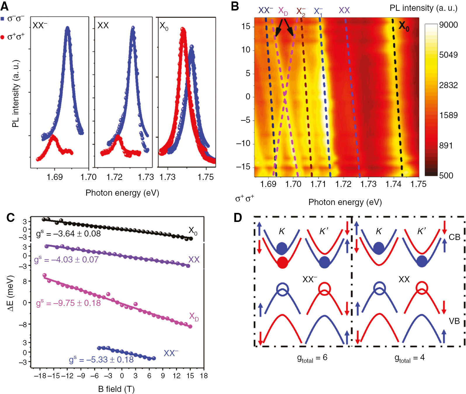
Biexciton and trion–exciton complexes in h-BN–encapsulated monolayer WSe2.
(A) Polarization-resolved PL spectra of the X0, XX, and XX− states (B=17 T). The XX and XX− states show the inverse PL intensity of the σ−σ− and σ+σ+ configurations, compared to the distinctively different behavior of the X0. (B) Magneto-PL spectra as a function of the out-of-plane magnetic field. The Zeeman shift of the XX and XX− is similar to the X0 with the redshift from −17 to 17 T. It is worth noting that the XD presents a unique X-pattern, originating from the out-of-plane radiation dipole. (C) The calculated g factor of different excitonic states from the linear fitting of Zeeman splitting between σ−σ− and σ+σ+ configurations. The g factors of XX and XX− states are −3.64 and −5.33, respectively, while the XD exhibits significantly larger g factor with the value of −9.75. (D) Schematic configurations of the trion–exciton and biexciton with the calculated total g factor of 6 and 4, respectively, where the solid dots represent the electrons and the empty circles for the holes. Blue color stands for spin up, and red for spin down.
The advancement of our understanding of the biexciton paves the way for the nonlinear quantum optoelectronics–based TMDCs.
4 Dark trions
Researchers have discovered that the tungsten-based TMDCs, like WSe2 and WS2, have a distinct band structure with both the splitting in the conduction and valence bands induced by the strong SOC [48], [49], [50], [51]. The resulted ground state is a spin-forbidden dark exciton due to the optical selection rule, which prevents it from direct recombination [75], [77], [112], [113], [114], [115], [116]. Zhang et al. [32] show that the in-plane magnetic field can brighten the dark excitons in monolayer WSe2, which exhibits much-increased emission and valley lifetimes due to the spin-forbidden configuration (Figure 6A, B). Park et al. [74] demonstrate the dramatically enhanced PL emission quantum yield (~6×10⁵-fold) of dark exciton through the coupling of the antenna tip to the dark exciton out-of-plane optical dipole moment using the monolayer WSe2 on a gold substrate at room temperature (Figure 6C). Zhou et al. [31] indicate that by the introduction of near-field coupling to surface plasmon polaritons (SPPs), the dark exciton and dark trions can be probed in monolayer TMDCs. The SPPs selectively couple with the out-of-plane dipole, which enables the enhancement of optical transition that is spin-forbidden. Therefore, when a piece of monolayer WSe2 is placed on a substrate covered with single-crystal silver film, the emission from near-field–coupled SPPs clearly shows the spectral features that are consistent with the energies and dipole orientations of the dark exciton and dark trions (Figure 6D, E). Wang et al. [78] investigate the optical transitions in monolayer WSe2, WS2, and MoSe2 by the polarization-resolved PL collecting from the edge of the sample. They observe clear signatures of the dark exciton, whose electric field is perpendicular to the monolayer plane, coinciding with the optical selection rules deduced from group theory analysis (Figure 6F). Nevertheless, is there a more direct way to observe these dark states?
![Figure 6: Dark exciton in monolayer WSe2.(A) Color plot of the PL spectra as a function of in-plane magnetic field measured from a monolayer WSe2 at 30 K. (B) Time-resolved PL from the bright exciton and dark trion under the in-plane magnetic field of 17.5 T at 4 K. The lifetime of dark trion is ~240 ps, whereas that of the bright exciton is less than 20 ps. (A, B) Adapted from Zhang et al. [32]. (C) Schematic of tip-enhanced PL spectroscopy and electronic band structure of monolayer WSe2. Selective excitation and probing of the transition dipole moments of dark (out-of-plane) and bright (in-plane) excitons by polarization control (adapted from Park et al. [74]). (D) Schematic of the experimental setup. TMDC monolayer and BN vdW structure is placed on top of single-crystal silver with silver acting as the backgate (Vg). Optical transitions can couple to both near-field SPPs and the FF, while the nanoscale trenches are used to detect the scattering signal into the FF from the coupling to SPPs. (E) Gate voltage–dependent FF-PL of the WSe2. New peaks of XD, XD+${\rm{X}}_{\rm{D}}^ + $ and XD−${\rm{X}}_{\rm{D}}^ - $ emerge in the neutral, p-doping, and n-doping regions, respectively. (D, E) Adapted from Zhou et al. [31]). (F) Detection of the PL from the edge of BN–encapsulated WSe2 sample at 13 K with the different detection polarizations [x is in the monolayer plane (green line), and z is perpendicular to it (red line)]. The schematic of detection method is shown in the inset of panel. Adapted from Wang et al. [78].](/document/doi/10.1515/nanoph-2020-0054/asset/graphic/j_nanoph-2020-0054_fig_006.jpg)
Dark exciton in monolayer WSe2.
(A) Color plot of the PL spectra as a function of in-plane magnetic field measured from a monolayer WSe2 at 30 K. (B) Time-resolved PL from the bright exciton and dark trion under the in-plane magnetic field of 17.5 T at 4 K. The lifetime of dark trion is ~240 ps, whereas that of the bright exciton is less than 20 ps. (A, B) Adapted from Zhang et al. [32]. (C) Schematic of tip-enhanced PL spectroscopy and electronic band structure of monolayer WSe2. Selective excitation and probing of the transition dipole moments of dark (out-of-plane) and bright (in-plane) excitons by polarization control (adapted from Park et al. [74]). (D) Schematic of the experimental setup. TMDC monolayer and BN vdW structure is placed on top of single-crystal silver with silver acting as the backgate (Vg). Optical transitions can couple to both near-field SPPs and the FF, while the nanoscale trenches are used to detect the scattering signal into the FF from the coupling to SPPs. (E) Gate voltage–dependent FF-PL of the WSe2. New peaks of XD,
Recently, Li et al. [29] apply the magneto-PL spectroscopy and Fourier plane imaging to investigate a top-gated single-layer WSe2, which results in unambiguous evidence to reveal the positive dark trion
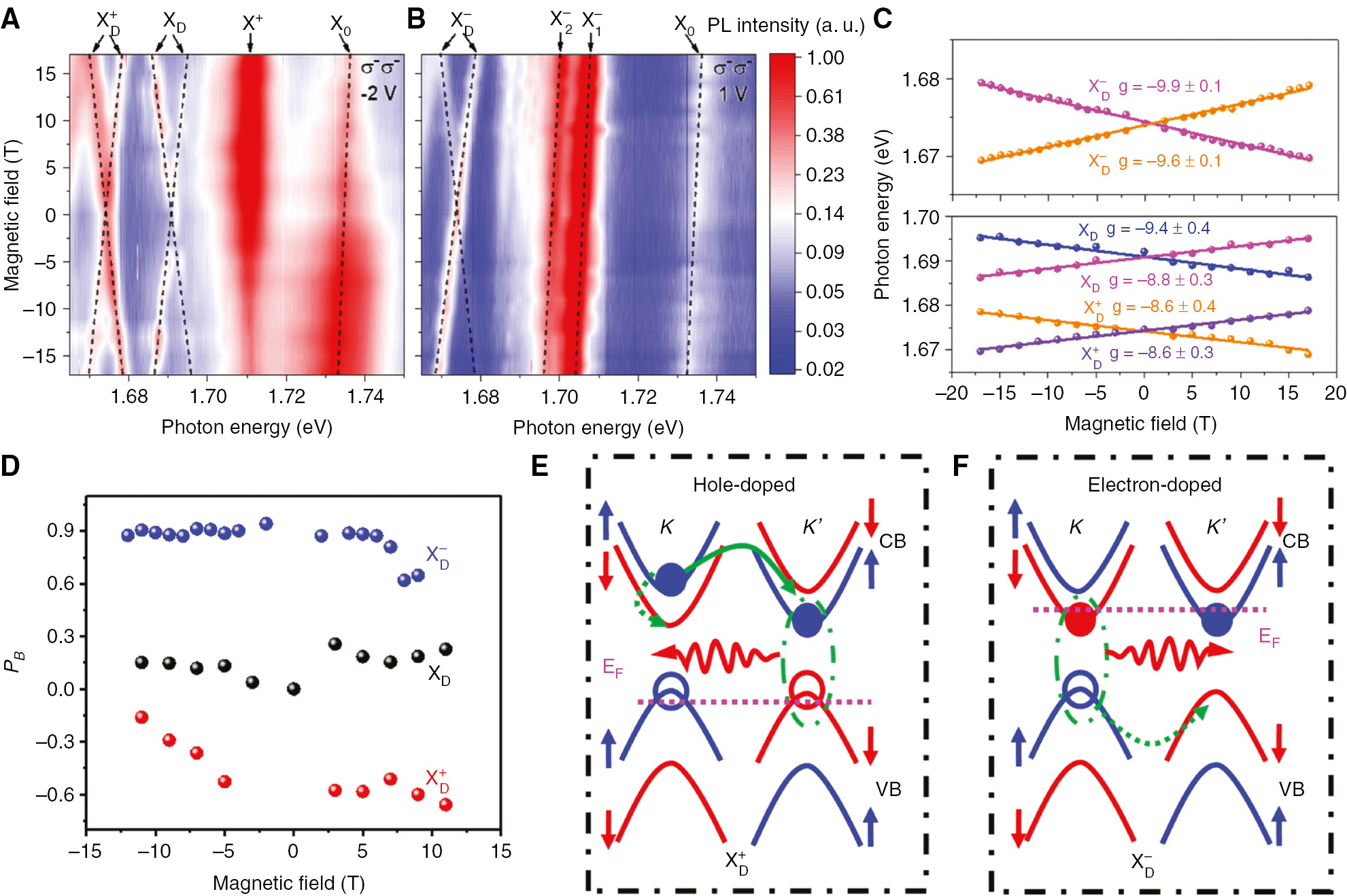
Positive and negative dark trions in h-BN–encapsulated monolayer WSe2.
(A, B) Magnetic field dependent PL spectra at the gate voltages of −2 and 1 V, corresponding to the hole-doping and electron-doping, respectively. Both the
Considering the complexity of the valley polarization of the dark trions, combined with the weak PL intensity of the negative dark trion, the “cross” pattern is often hard to be resolved. However, the dark trions also radiate through the out-of-plane dipole as the dark exciton, and the radiation pattern of the dark trion should be similar to the dark exciton; direct measurement of the radiation pattern will provide more direct and unambiguous evidence of the dark trions. It has been proven that the radiation pattern of dark exciton has significantly different features from the bright exciton [28]. Figure 8 is the Fourier plane imaging of different excitonic states. It is distinctively shown that the
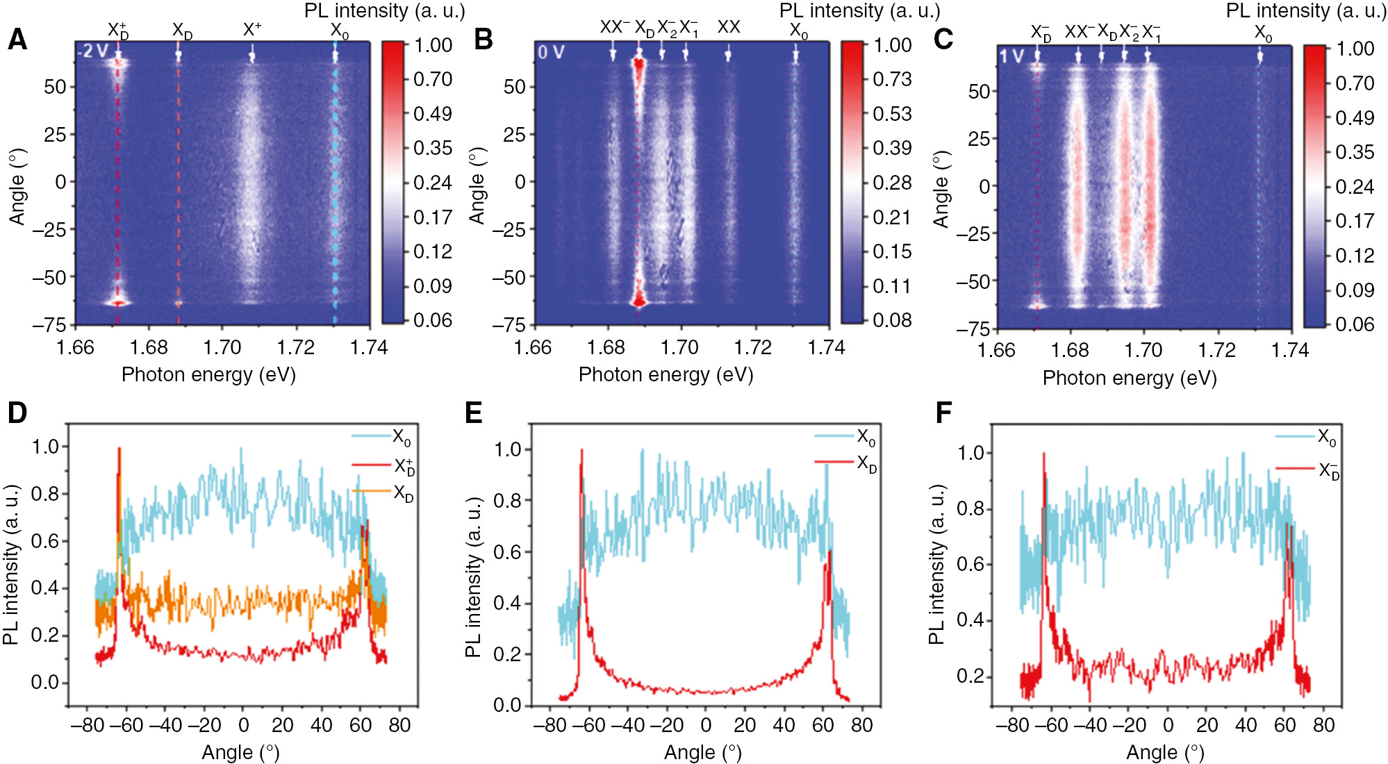
Fourier plane imaging of the different excitonic states.
(A–C) The radiation angle and photon energy–dependent PL spectra color plots of the gate voltages of −2, 0, and 1 V, respectively, corresponding to the
It is worth noting that a relevant work also reported on the measurement of the dark trions by the continuous tunability of the electrostatic gating from hole-doping to the electron-doping region [30]. The magneto-PL and TRPL reveal that the dark trions have distinct valley optical emission and the lifetime from 0.4 to 1.3 ns.
5 Exciton–phonon interaction
In monolayer TMDCs, the exciton–phonon interaction plays an important role in the relaxation dynamics of excitonic states. Due to the unique band structure of monolayer TMDCs, the interband transitions of electrons in the intravalley and intervalley processes will involve the absorption or emission of the phonons locating at the Г and K points, respectively, due to the conservation of momentum. Figure 9A shows the phonon dispersion spectrum of the monolayer WSe2. Many theoretical and experimental works have contributed to the signature of the strong exciton–phonon interaction in the exciton dynamics [16], [35], [60], [120], [121], [122], [123], [124], [125], [126]. For example, double-resonant Raman scattering reveals the preservation of the valley coherence in monolayer WSe2 [127]; excitons enhance the anti-Stokes shifts in monolayer MoTe2 [128]; A1′ phonons assist the trion to exciton luminescence upconversion in monolayer WSe2 [129]. Most importantly, the phonon with helicity has been recently theoretically proposed [31] and experimentally reported [36], [37]. Among them, the E″ mode chiral phonon at the Г point and the E′ mode chiral phonon at the K point are studied extensively in the exciton–phonon interaction (Figure 9B). For the E′ (K) phonon, the tungsten atom is stationary, whereas the selenium has a clockwise (or anticlockwise) rotation in K (or K′) valley with a 2/3π phase difference. The E′ (K) phonon has been previously observed experimentally by investigating the transition between A and B exciton states with transient infrared (IR) spectroscopy (Figure 9C). The left circularly polarized light pumps holes to move from K to K′ valley by creating a LO(K) phonon and simultaneously absorbs an IR probe photon, relaxing to the lower valence band in the opposite valley and emitting right circularly polarized photon [36]. For E″ (Г) phonon, there are two degenerate modes in which the tungsten atom is stationary, whereas the selenium atoms can vibrate in two orthogonal in-plane directions. The superposition of these two orthogonal linear vibrations results in the left- or right-handed chiral phonon, with the angular momentum of 1 or −1, respectively. Figure 9D reveals the E″ (Г) phonon replicas of the quantum dots in monolayer WSe2 [34]. The quantum dots can couple with the E″ (Г), leading to the emission of the phonon replica, and the energy spacing is always 21.8 meV, which is the energy of E″ (Г) mode.
![Figure 9: Fourier plane imaging of the different excitonic states.(A) Phonon dispersion curve for monolayer WSe2. Adapted from Yuan et al. [119]. (B) Schematic of E″ mode chiral phonon at the Г point and the E′ mode chiral phonon at the K point. (C) Hole–phonon interaction in the transition between A to B exciton in the monolayer WSe2 through pump-probe measurement. Adapted from Zhu et al. [36]. (D) E″ (Г) phonon replicas of the quantum dots in monolayer WSe2. The energy spacing between a and b doublets is 21.8 meV, which is consistent with the energy of the E″ (Г) phonon. Adapted from Chen et al. [34].](/document/doi/10.1515/nanoph-2020-0054/asset/graphic/j_nanoph-2020-0054_fig_009.jpg)
Fourier plane imaging of the different excitonic states.
(A) Phonon dispersion curve for monolayer WSe2. Adapted from Yuan et al. [119]. (B) Schematic of E″ mode chiral phonon at the Г point and the E′ mode chiral phonon at the K point. (C) Hole–phonon interaction in the transition between A to B exciton in the monolayer WSe2 through pump-probe measurement. Adapted from Zhu et al. [36]. (D) E″ (Г) phonon replicas of the quantum dots in monolayer WSe2. The energy spacing between a and b doublets is 21.8 meV, which is consistent with the energy of the E″ (Г) phonon. Adapted from Chen et al. [34].
5.1 Dark exciton phonon replica
Tungsten-based monolayer transition metal dichalcogenides host a long-lived “dark” exciton [75], [77], [113], [114], [115], [116], [130], [131], [132], an electron–hole pair in a spin-triplet configuration. The long lifetime and unique spin properties of the dark exciton provide exciting opportunities to explore light–matter interactions beyond electric dipole transitions. In bright excitons, the in-plane transition dipole in K (or K′) valley can selectively couple with the left (or right) circularly polarized light, which empowers us to conveniently access the valley information. However, the valley selection rule for dark exciton is distinctively different from the bright exciton. The dark exciton with an out-of-plane transition dipole can couple with both left and right circular lights, which make it difficult to distinguish the valley pseudospin of dark states. To overcome this limitation, careful maneuvering of the selection rules through higher-order interactions provides access to the otherwise dark states and reveals additional rich physics.
It has been reported that the coupling of the dark exciton and an optically silent chiral phonon enables the intrinsic PL of the dark-exciton replica in single-layer WSe2 [33]. The gate voltage–dependent PL spectra reveal that the XD and
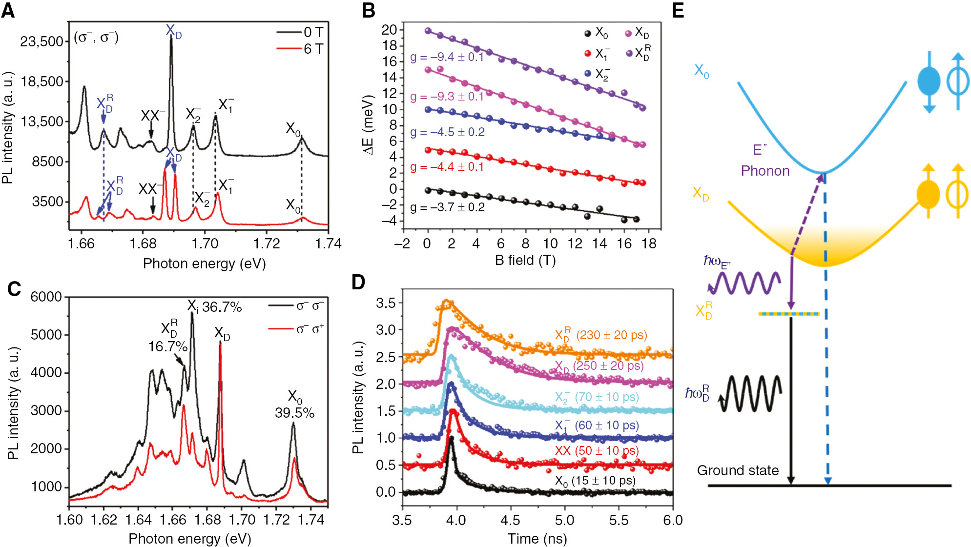
Phonon replica of dark exciton in h-BN–encapsulated monolayer WSe2.
(A) Valley-resolved PL spectra without magnetic field and with 6-T out-of-plane magnetic field at 4.2 K, using an objective of large numerical aperture (N.A.: ~0.60). Both the XD and
5.2 Intervalley exciton
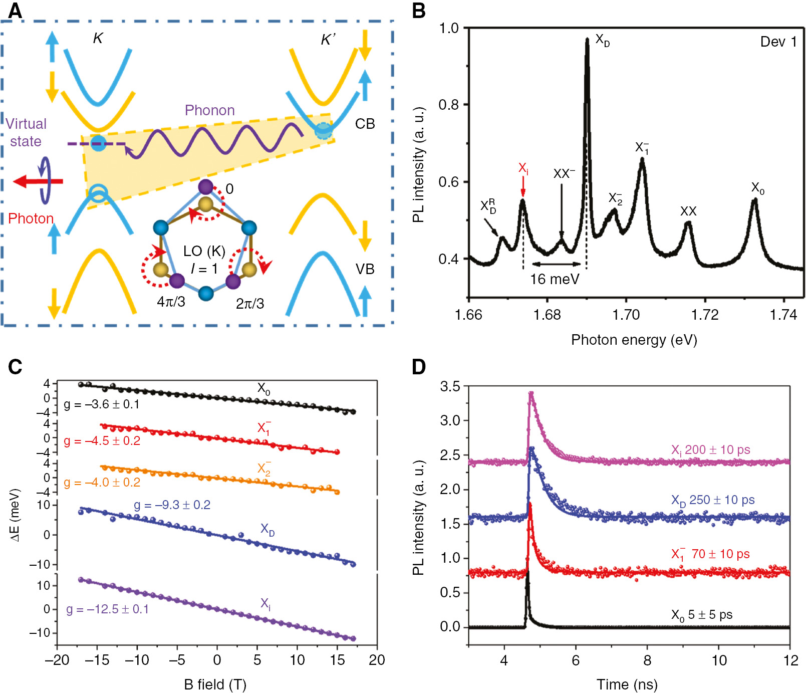
Not only the spin-forbidden dark exciton can couple with the chiral phonon to emit the phonon replica with circular polarization, but also the momentum-forbidden intervalley dark exciton interacts with the chiral phonon locating at K point, resulting in the emission of circularly polarized light [35]. Assuming the circularly polarized excitation occurring in the K valley, the intervalley exciton consists of one electron in the K′ valley and one hole in the K valley. The electron transits to a virtual state in the K valley by emitting a chiral phonon and then recombines with the hole in the valence band of the same valley, emitting a photon with certain helicity (Figure 11A). As shown in Figure 11B, peak Xi always emerges between the
Intervalley exciton in h-BN–encapsulated monolayer WSe2.
(A) Schematic of the intervalley exciton and chiral phonon coupling. The intervalley exciton consists of one electron and one hole in the different valleys. The electron can transit to a virtual state locating at the hole-sitting valley by emitting a chiral phonon and then recombining with the hole, emitting a circular photon. Inset: schematic representation of the E′ chiral phonon mode at the K point. Blue sphere: W atom. Yellow and purple spheres are Se atoms in the equilibrium state and the vibration state, respectively. (B) Photoluminescence spectrum of monolayer WSe2. Besides the established excitonic states, a novel peak Xi locates between the phonon replica of the dark exciton
5.3 Interlayer phonon coupling
Emerging phonon mode has also been recently discovered in vdW heterostructure of TMDCs due to strong exciton–phonon interactions. It has been demonstrated that the Raman scattering process between the interface of the WSe2/SiO2 and WSe2/h-BN can enable the Raman scattering with either traditionally inactive or weak; therefore, the PL intensity will be modulated by the exciton–phonon coupling, as the PLE spectra shown in Figure 12A–C [22]. Especially, when the phonon modes are coupled with the A exciton directly or via an
![Figure 12: Interlayer exciton–phonon interaction between h-BN and monolayer WSe2.(A–C) PLE intensity as a function of the excess energy of the energy difference between the excitation source and emission for WSe2/SiO2, h-BN/WSe2/SiO2, and h-BN/WSe2/h-BN/SiO2 structures, respectively. Adapted from Chow et al. [22]. (D) Photoluminescence emission from h-BN/WSe2/h-BN sandwiched structure under the excitation energies of 1.849, 1.857, and 1.862 eV. Two Raman peaks (green and orange arrows) emerge, and their peak positions shift linearly with the incident laser energy. (E) Reflection spectroscopy of h-BN/WSe2/h-BN sandwiched structure (red) and pristine WSe2 (black) at 77 K. A new peak at 1.85 eV emerges in the sandwiched structure due to the interlayer exciton–phonon coupling. (D, E) Adapted from Jin et al. [23].](/document/doi/10.1515/nanoph-2020-0054/asset/graphic/j_nanoph-2020-0054_fig_012.jpg)
Interlayer exciton–phonon interaction between h-BN and monolayer WSe2.
(A–C) PLE intensity as a function of the excess energy of the energy difference between the excitation source and emission for WSe2/SiO2, h-BN/WSe2/SiO2, and h-BN/WSe2/h-BN/SiO2 structures, respectively. Adapted from Chow et al. [22]. (D) Photoluminescence emission from h-BN/WSe2/h-BN sandwiched structure under the excitation energies of 1.849, 1.857, and 1.862 eV. Two Raman peaks (green and orange arrows) emerge, and their peak positions shift linearly with the incident laser energy. (E) Reflection spectroscopy of h-BN/WSe2/h-BN sandwiched structure (red) and pristine WSe2 (black) at 77 K. A new peak at 1.85 eV emerges in the sandwiched structure due to the interlayer exciton–phonon coupling. (D, E) Adapted from Jin et al. [23].
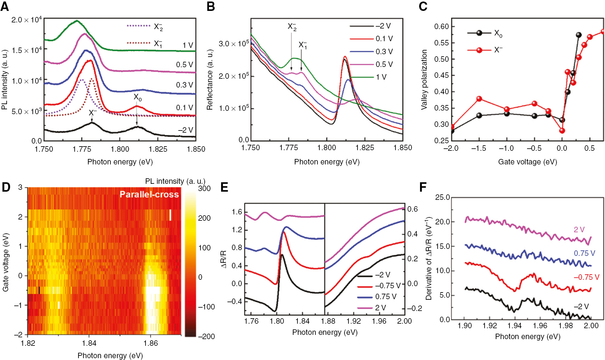
This emerging Raman mode due to strong exciton–phonon interaction has also been found in TMDC alloys, which has tunable optical bandgaps [133], [134], [135], [136], [137], [138], [139], [140], [141], [142], [143], [144], [145], [146], [147], [148], [149], [150], such as WS2xSe2(1−x) and MoxW1−xSe2. Recently, the high-quality h-BN–encapsulated monolayer WS0.6Se1.4 is demonstrated to inherit the superior optical properties of tungsten-based TMDCs [39]. Both the PL and reflection spectra show that both the exciton and trion peaks emerge in monolayer WS0.6Se1.4. The trion has the fine structure of the intervalley and intravalley trions with the exchange interaction induced splitting energy of ~6 meV (Figure 13A, B), similar to that of WSe2 or WS2. The valley-resolved PL spectra indicate that both the exciton and trion of monolayer WS0.6Se1.4 possess the gate tunable valley polarization with the value as high as ~60% in the charge-neutral region (Figure 13C). Another interesting phenomenon is that the exciton–phonon coupling in the h-BN/WS0.6Se1.4/h-BN vdW heterostructure can also be tuned by the gate voltage, which renders the optical silent Raman mode visible (Figure 13D). In addition, the reflection contrast and its differential of monolayer WS0.6Se1.4 also show an absorption resonance at ~1.945 eV, 140 meV above the A exciton energy. This 140 meV is roughly the same as the energy difference between the new resonance and A exciton in WSe2. Considering the similar dielectric constant between WS0.6Se1.4 and WSe2, the new resonance found in the WS0.6Se1.4 is of the same nature of the WSe2 and is consistent with the reported value of the energy difference between 1s and 2s exciton of WSe2 [68], [72]. The emerging resonance in the absorption spectra, which corresponds to the second resonance of the exciton-phonon coupling, was then confirmed to be the 2s state of the A exciton (Figure 13E, F). The Raman signals are therefore dramatically enhanced when the excitation is in resonance with the energy of the 2s state of A exciton.
Excitonic states and exciton–phonon coupling in h-BN sandwiched WSe2.
(A) Light emission of monolayer WS0.6Se1.4 as a function of the gate voltage at 14 K. The monolayer alloy clearly shows the emissions of the exciton and trion. The trion also exhibits the fine structure of the intervalley and intravalley trions. (B) Gate voltage–dependent reflection spectroscopy of monolayer WS0.6Se1.4. Similar to the PL spectra, the reflection spectra show the absorption of exciton and trion, which also indicates the intervalley and intravalley trions fine structures. (C) The degree of valley polarization of exciton and trion from valley-resolved PL spectra as a function of the gate voltage. Both the valley polarization of exciton and trion increase with the gate voltage from −2 to 1 V. (D) Color plot of PL spectrum difference between the parallel and cross configuration as a function of the gate voltage at 77 K, which clearly presents the two Raman scattering peaks. (E) Gate voltage–dependent differential reflectance spectra of the monolayer WS0.6Se1.4. (F) Derivative of the differential reflectance spectra of the monolayer WS0.6Se1.4 as a function of the gate voltage at 14 K. A new feature X* at ~1.945 eV shows up in the charge-neutral region, corresponding to the 2s state of A exciton.
6 Conclusions and perspective
The significant improvement of the sample quality greatly advances our understanding of many-particle excitonic physics in the TMDCs, enabled by the well-resolved and tunable optical spectra signatures. The BN-encapsulated TMDC monolayer and associated vdW heterostructure devices therefore provide fascinating platforms to investigate the 2D excitonic physics and many-body interactions. Although many of the excitonic fine features have been revealed in monolayer TMDCs, how would they affect the optical spectra of the twisted bilayer TMDCs? Moiré potential, controlled by the twist angle of the bilayer, has been shown to significantly modulate the intralayer or interlayer excitons. How would they affect the many-body physics such as the exciton–phonon interactions or exciton–polarons? Is it possible to use any of the many-body interactions to manipulate the valley degree of freedoms? Many intriguing questions remain to be addressed, and we expect to see even more exciting advancement in this field in the near future.
Acknowledgments
This work is primarily supported by AFSOR through grant no. FA9550-18-1-0312, Funder Id: http://dx.doi.org/10.13039/100000181. Z. Li also acknowledges supports from the Shanghai Sailing Program (grant no. 19YF1425200) and the National Natural Science Foundation for Young Scientists Fund of China (grant no. 51902196). T. Wang acknowledges support from ACS PRF through grant 59957-DNI10, Funder Id: http://dx.doi.org/10.13039/100006770. Z. Lian acknowledges support from NYSTAR through Focus Center-NY-RPI Contract C150117. S.-F. Shi also acknowledges the support from a KIP grant from RPI.
References
[1] Novoselov KS, Geim AK, Morozov SV, et al. Electric field effect in atomically thin carbon films. Science 2004;306:666–9.10.1126/science.1102896Search in Google Scholar PubMed
[2] Novoselov KS, Geim AK, Morozov SV, et al. Two-dimensional gas of massless Dirac fermions in graphene. Nature 2005;438:197–200.10.1038/nature04233Search in Google Scholar PubMed
[3] Zhang Y, Tan YW, Stormer HL, Kim P. Experimental observation of the quantum Hall effect and Berry’s phase in graphene. Nature 2005;438:201–4.10.1038/nature04235Search in Google Scholar PubMed
[4] Chakraborty C, Vamivakas N, Englund D. Advances in quantum light emission from 2D materials. Nanophotonics 2019;8:2017–32.10.1515/nanoph-2019-0140Search in Google Scholar
[5] Liu Y, Duan X, Huang Y, Duan X. Two-dimensional transistors beyond graphene and TMDCs. Chem Soc Rev 2018:6388–409.10.1039/C8CS00318ASearch in Google Scholar
[6] Zhu C, Gao D, Ding J, Chao D, Wang J. TMD-based highly efficient electrocatalysts developed by combined computational and experimental approaches. Chem Soc Rev 2018;47:4332–56.10.1039/C7CS00705ASearch in Google Scholar
[7] Schulman DS, Arnold AJ, Das S. Contact engineering for 2D materials and devices. Chem Soc Rev 2018;47:3037–58.10.1039/C7CS00828GSearch in Google Scholar PubMed
[8] Chen P, Zhang Z, Duan X, Duan X. Chemical synthesis of two-dimensional atomic crystals, heterostructures and superlattices. Chem Soc Rev 2018;47:3129–51.10.1039/C7CS00887BSearch in Google Scholar
[9] Li X, Zhi L. Graphene hybridization for energy storage applications. Chem Soc Rev 2018;47:3189–216.10.1039/C7CS00871FSearch in Google Scholar
[10] Garcia JH, Vila M, Cummings AW, Roche S. Spin transport in graphene/transition metal dichalcogenide heterostructures. Chem Soc Rev 2018;47:3359–79.10.1039/C7CS00864CSearch in Google Scholar PubMed
[11] Yi F, Ren H, Shan J, Sun X, Wei D, Liu Z. Wearable energy sources based on 2D materials. Chem Soc Rev 2018;47:3152–88.10.1039/C7CS00849JSearch in Google Scholar
[12] Wang QH, Kalantar-Zadeh K, Kis A, Coleman JN, Strano MS. Electronics and optoelectronics of two-dimensional transition metal dichalcogenides. Nat Nanotechnol 2012;7:699–712.10.1038/nnano.2012.193Search in Google Scholar PubMed
[13] Mueller T, Malic E. Exciton physics and device application of two-dimensional transition metal dichalcogenide semiconductors. NPJ 2D Mater Appl 2018;2:29.10.1038/s41699-018-0074-2Search in Google Scholar
[14] Gustafsson MV, Yankowitz M, Forsythe C, et al. Ambipolar Landau levels and strong band-selective carrier interactions in monolayer WSe2. Nat Mater 2018;17:411–5.10.1038/s41563-018-0036-2Search in Google Scholar PubMed
[15] Zhang X, Lou F, Li C, et al. Flux method growth of bulk MoS2 single crystals and their application as a saturable absorber. CrystEngComm 2015;17:4026–32.10.1039/C5CE00484ESearch in Google Scholar
[16] Rhodes D, Chae SH, Ribeiro-Palau R, Hone J. Disorder in van der Waals heterostructures of 2D materials. Nat Mater 2019;18:541–9.10.1038/s41563-019-0366-8Search in Google Scholar PubMed
[17] Edelberg D, Rhodes D, Kerelsky A, et al. Approaching the intrinsic limit in transition metal diselenides via point defect control. Nano Lett 2019;19:4371–9.10.1021/acs.nanolett.9b00985Search in Google Scholar PubMed
[18] Rhodes D, Schönemann R, Aryal N, et al. Bulk Fermi surface of the Weyl type-II semimetallic candidate γ-MoTe2. Phys Rev B 2017;96:165134.10.1103/PhysRevB.96.165134Search in Google Scholar
[19] Yan JQ, Sales BC, Susner MA, McGuire MA. Flux growth in a horizontal configuration: an analog to vapor transport growth. Phys Rev Mater 2017;1:1–11.10.1103/PhysRevMaterials.1.023402Search in Google Scholar
[20] Taniguchi T, Watanabe K. Synthesis of high-purity boron nitride single crystals under high pressure by using Ba–BN solvent. J Cryst Growth 2007;303:525–9.10.1016/j.jcrysgro.2006.12.061Search in Google Scholar
[21] Manca M, Glazov MM, Robert C, et al. Enabling valley selective exciton scattering in monolayer WSe2 through upconversion. Nat Commun 2017;8:14927.10.1038/ncomms14927Search in Google Scholar PubMed PubMed Central
[22] Chow CM, Yu H, Jones AM, et al. Unusual exciton–phonon interactions at van der Waals engineered interfaces. Nano Lett 2017;17:1194–9.10.1021/acs.nanolett.6b04944Search in Google Scholar PubMed
[23] Jin C, Kim J, Suh J, et al. Interlayer electron–phonon coupling in WSe2/hBN heterostructures. Nat Phys 2016;13:127–31.10.1038/nphys3928Search in Google Scholar
[24] Wang Z, Shan J, Mak KF. Valley- and spin-polarized Landau levels in monolayer WSe2. Nat Nanotechnol 2017;12:144–9.10.1038/nnano.2016.213Search in Google Scholar PubMed
[25] Li Z, Wang T, Lu Z, et al. Revealing the biexciton and trion–exciton complexes in BN encapsulated WSe2. Nat Commun 2018;9:3719.10.1038/s41467-018-05863-5Search in Google Scholar PubMed PubMed Central
[26] Barbone M, Montblanch AR-P, Kara DM, et al. Charge-tuneable biexciton complexes in monolayer WSe2. Nat Commun 2018;9:3721.10.1038/s41467-018-05632-4Search in Google Scholar PubMed PubMed Central
[27] Chen S-Y, Goldstein T, Taniguchi T, Watanabe K, Yan J. Coulomb-bound four- and five-particle intervalley states in an atomically-thin semiconductor. Nat Commun 2018;9:3717.10.1038/s41467-018-05558-xSearch in Google Scholar PubMed PubMed Central
[28] Ye Z, Waldecker L, Ma EY, et al. Efficient generation of neutral and charged biexcitons in encapsulated WSe2 monolayers. Nat Commun 2018;9:3718.10.1038/s41467-018-05917-8Search in Google Scholar PubMed PubMed Central
[29] Li Z, Wang T, Lu Z, et al. Direct observation of gate-tunable dark trions in monolayer WSe2. Nano Lett 2019;19:6886–93.10.1021/acs.nanolett.9b02132Search in Google Scholar PubMed
[30] Liu E, van Baren J, Lu Z, et al. Gate tunable dark trions in monolayer WSe2. Phys Rev Lett 2019;123:027401.10.1103/PhysRevLett.123.027401Search in Google Scholar PubMed
[31] Zhou Y, Scuri G, Wild DS, et al. Probing dark excitons in atomically thin semiconductors via near-field coupling to surface plasmon polaritons. Nat Nanotechnol 2017;12:856–60.10.1038/nnano.2017.106Search in Google Scholar PubMed
[32] Zhang XX, Cao T, Lu Z, et al. Magnetic brightening and control of dark excitons in monolayer WSe2. Nat Nanotechnol 2017;12:883–8.10.1038/nnano.2017.105Search in Google Scholar PubMed
[33] Li Z, Wang T, Jin C, et al. Emerging photoluminescence from the dark-exciton phonon replica in monolayer WSe2. Nat Commun 2019;10:2469.10.1038/s41467-019-10477-6Search in Google Scholar PubMed PubMed Central
[34] Chen X, Lu X, Dubey S, et al. Entanglement of single-photons and chiral phonons in atomically thin WSe2. Nat Phys 2018;15:221–8.10.1038/s41567-018-0366-7Search in Google Scholar
[35] Li Z, Wang T, Jin C, et al. Momentum-dark intervalley exciton in monolayer tungsten diselenide brightened via chiral phonon. ACS Nano 2019;13:14107–13.10.1021/acsnano.9b06682Search in Google Scholar PubMed
[36] Zhu H, Yi J, Li MY, et al. Observation of chiral phonons. Science 2018;359:579–82.10.1126/science.aar2711Search in Google Scholar PubMed
[37] Zhang L, Niu Q, Phonon VI. Chiral phonons at high-symmetry points in monolayer hexagonal lattices. Phys Rev Lett 2015;115:115502.10.1103/PhysRevLett.115.115502Search in Google Scholar PubMed
[38] Liu E, Van Baren J, Lu Z, Taniguchi T, Watanabe K. Valley-selective chiral phonon replicas of dark excitons and trions in monolayer WSe2. Phys Rev Res 2019;1:032007.10.1103/PhysRevResearch.1.032007Search in Google Scholar
[39] Meng Y, Wang T, Li Z, et al. Excitonic complexes and emerging interlayer electron–phonon coupling in BN encapsulated monolayer semiconductor alloy: WS0.6Se1.4. Nano Lett 2019;19:299–307.10.1021/acs.nanolett.8b03918Search in Google Scholar PubMed
[40] Chow CM, Yu H, Jones AM, et al. Phonon-assisted oscillatory exciton dynamics in monolayer MoSe2. Npj 2D Mater Appl 2017;1:33.10.1038/s41699-017-0035-1Search in Google Scholar
[41] Liu X, Hersam MC. 2D materials for quantum information science. Nat Rev Mater 2019;4:669–84.10.1038/s41578-019-0136-xSearch in Google Scholar
[42] Mak KF, Lee C, Hone J, Shan J, Heinz TF. Atomically thin MoS2: a new direct-gap semiconductor. Phys Rev Lett 2010;105:136805.10.1103/PhysRevLett.105.136805Search in Google Scholar PubMed
[43] Splendiani A, Sun L, Zhang Y, et al. Emerging photoluminescence in monolayer MoS2. Nano Lett 2010;10:1271–5.10.1021/nl903868wSearch in Google Scholar PubMed
[44] Cao T, Wang G, Han W, et al. Valley-selective circular dichroism of monolayer molybdenum disulphide. Nat Commun 2012;3:887.10.1038/ncomms1882Search in Google Scholar PubMed PubMed Central
[45] Mak KF, He K, Shan J, Heinz TF. Control of valley polarization in monolayer MoS2 by optical helicity. Nat Nanotechnol 2012;7:494–8.10.1038/nnano.2012.96Search in Google Scholar PubMed
[46] Mak KF, Shan J. Photonics and optoelectronics of 2D semiconductor transition metal dichalcogenides. Nat Photonics 2016;10:216–26.10.1038/nphoton.2015.282Search in Google Scholar
[47] Sie EJ, McLver JW, Lee YH, Fu L, Kong J, Gedik N. Valley-selective optical Stark effect in monolayer WS2. Nat Mater 2015;14:290–4.10.1007/978-3-319-69554-9_4Search in Google Scholar
[48] Xiao D, Liu G-B, Feng W, Xu X, Yao W. Coupled spin and valley physics in monolayers of MoS2 and other group-VI dichalcogenides. Phys Rev Lett 2012;108:196802.10.1103/PhysRevLett.108.196802Search in Google Scholar PubMed
[49] Liu G-B, Shan WY, Yao Y, Yao W, Xiao D. Three-band tight-binding model for monolayers of group-VIB transition metal dichalcogenides. Phys Rev B 2013;88:085433.10.1103/PhysRevB.88.085433Search in Google Scholar
[50] Wang G, Chernikov A, Glazov MM, et al. Excitons in atomically thin transition metal dichalcogenides. Rev Mod Phys 2017;90:021001.10.1103/RevModPhys.90.021001Search in Google Scholar
[51] Liu G-B, Xiao D, Yao Y, Xu X, Yao W. Electronic structures and theoretical modelling of two-dimensional group-VIB transition metal dichalcogenides. Chem Soc Rev 2015;44:2643–63.10.1039/C4CS00301BSearch in Google Scholar
[52] Zeng H, Dai J, Yao W, Xiao D, Cui X. Valley polarization in MoS2 monolayers by optical pumping. Nat Nanotechnol 2012;7:490–3.10.1038/nnano.2012.95Search in Google Scholar PubMed
[53] Xu X, Yao W, Xiao D, Heinz TF. Spin and pseudospins in layered transition metal dichalcogenides. Nat Phys 2014;10:343–50.10.1038/nphys2942Search in Google Scholar
[54] Wang G, Chernikov A, Glazov MM, et al. Colloquium: excitons in atomically thin transition metal dichalcogenides. Rev Mod Phys 2018;90:21001.10.1103/RevModPhys.90.021001Search in Google Scholar
[55] Wang Z, Shan J, Mak KF. Valley- and spin-polarized Landau levels in monolayer WSe2. Nat Nanotechnol 2016;12:144–9.10.1038/nnano.2016.213Search in Google Scholar PubMed
[56] Jin C, Kim J, Iqbal Bakti Utama M, et al. Imaging of pure spin-valley diffusion current in WS2-WSe2 heterostructures. Science 2018;360:893–6.10.1126/science.aao3503Search in Google Scholar PubMed
[57] Wang K, De Greve K, Jauregui LA, et al. Electrical control of charged carriers and excitons in atomically thin materials. Nat Nanotechnol 2018;13:128–32.10.1038/s41565-017-0030-xSearch in Google Scholar PubMed
[58] Wang Z, Mak KF, Shan J. Strongly interaction-enhanced valley magnetic response in monolayer WSe2. Phys Rev Lett 2018;120:066402.10.1103/PhysRevLett.120.066402Search in Google Scholar PubMed
[59] Manchon A, Koo HC, Nitta J, Frolov SM, Duine RA. New perspectives for Rashba spin-orbit coupling. Nat Mater 2015;14:871–82.10.1038/nmat4360Search in Google Scholar PubMed
[60] Rycerz A, Tworzydło J, Beenakker CWJ. Valley filter and valley valve in graphene. Nat Phys 2007;3:172–5.10.1038/nphys547Search in Google Scholar
[61] Vitale SA, Nezich D, Varghese JO, et al. Valleytronics: opportunities, challenges, and paths forward. Small 2018;14:1801483.10.1002/smll.201801483Search in Google Scholar PubMed
[62] Schaibley JR, Yu H, Clark G, et al. Valleytronics in 2D materials. Nat Rev Mater 2016;1:16055.10.1038/natrevmats.2016.55Search in Google Scholar
[63] Jones AM, Yu H, Ghimire NJ, et al. Optical generation of excitonic valley coherence in monolayer WSe2. Nat Nanotechnol 2013;8:634–8.10.1038/nnano.2013.151Search in Google Scholar PubMed
[64] Hu G, Hong X, Wang K, et al. Coherent steering of nonlinear chiral valley photons with a synthetic Au–WS2 metasurface. Nat Photonics 2019;13:467–72.10.1038/s41566-019-0399-1Search in Google Scholar
[65] Liu Y, Gao Y, Zhang S, He J, Yu J, Liu Z. Valleytronics in transition metal dichalcogenides materials. Nano Res 2019;12:2695–711.10.1007/s12274-019-2497-2Search in Google Scholar
[66] Ye Z, Sun D, Heinz TF. Optical manipulation of valley pseudospin. Nat Phys 2017;13:26–9.10.1038/nphys3891Search in Google Scholar
[67] Eda G, Maier SA. Two-dimensional crystals: managing light for optoelectronics. ACS Nano 2013;7:5660–5.10.1021/nn403159ySearch in Google Scholar PubMed
[68] Chernikov A, Berkelbach TC, Hill HM, et al. Exciton binding energy and nonhydrogenic Rydberg series in monolayer WS2. Phys Rev Lett 2014;113:076802.10.1103/PhysRevLett.113.076802Search in Google Scholar PubMed
[69] Raja A, Chaves A, Yu J, et al. Coulomb engineering of the bandgap and excitons in two-dimensional materials. Nat Commun 2017;8:15251.10.1038/ncomms15251Search in Google Scholar PubMed PubMed Central
[70] Hill HM, Rigosi AF, Roquelet C, et al. Observation of excitonic Rydberg states in monolayer MoS2 and WS2 by photoluminescence excitation spectroscopy. Nano Lett 2015;15:2992–7.10.1021/nl504868pSearch in Google Scholar PubMed
[71] Yu H, Bin Liu G, Gong P, Xu X, Yao W. Dirac cones and Dirac saddle points of bright excitons in monolayer transition metal dichalcogenides. Nat Commun 2014;5:3876.10.1038/ncomms4876Search in Google Scholar PubMed
[72] He K, Kumar N, Zhao L, et al. Tightly bound excitons in monolayer WSe2. Phys Rev Lett 2014;113:026803.10.1103/PhysRevLett.113.026803Search in Google Scholar PubMed
[73] Ross JS, Wu S, Yu H, et al. Electrical control of neutral and charged excitons in a monolayer semiconductor. Nat Commun 2013;4:1474.10.1038/ncomms2498Search in Google Scholar PubMed
[74] Park KD, Jiang T, Clark G, Xu X, Raschke MB. Radiative control of dark excitons at room temperature by nano-optical antenna-tip Purcell effect. Nat Nanotechnol 2018;13:59–64.10.1038/s41565-017-0003-0Search in Google Scholar PubMed
[75] Zhang XX, You Y, Zhao SYF, Heinz TF. Experimental evidence for dark excitons in monolayer WSe2. Phys Rev Lett 2015;115:257403.10.1103/PhysRevLett.115.257403Search in Google Scholar PubMed
[76] Robert C, Amand T, Cadiz F, et al. Fine structure and lifetime of dark excitons in transition metal dichalcogenide monolayers. Phys Rev B 2017;96:155423.10.1103/PhysRevB.96.155423Search in Google Scholar
[77] Tang Y, Mak KF, Shan J. Long valley lifetime of dark excitons in single-layer WSe2. Nat Commun 2019;10:4047.10.1038/s41467-019-12129-1Search in Google Scholar PubMed PubMed Central
[78] Wang G, Robert C, Glazov MM, et al. In-plane propagation of light in transition metal dichalcogenide monolayers: optical selection rules. Phys Rev Lett 2017;119:047401.10.1103/PhysRevLett.119.047401Search in Google Scholar PubMed
[79] Singh A, Tran K, Kolarczik M, et al. Long-lived valley polarization of intravalley trions in monolayer WSe2. Phys Rev Lett 2016;117:257402.10.1103/PhysRevLett.117.257402Search in Google Scholar PubMed
[80] Plechinger G, Nagler P, Arora A, et al. Trion fine structure and coupled spin-valley dynamics in monolayer tungsten disulfide. Nat Commun 2016;7:12715.10.1038/ncomms12715Search in Google Scholar PubMed PubMed Central
[81] Tartakovskii AI. The valley Zeeman effect in inter- and intra-valley trions in monolayer WSe2. Nat Commun 2019;10:2330.10.1038/s41467-019-10228-7Search in Google Scholar PubMed PubMed Central
[82] Mak KF, He K, Lee C, et al. Tightly bound trions in monolayer MoS2. Nat Mater 2012;12:207–11.10.1038/nmat3505Search in Google Scholar PubMed
[83] Van Der Donck M, Zarenia M, Peeters FM, Van Der Donck M, Zarenia M, Peeters FM. Excitons, trions, and biexcitons in transition-metal dichalcogenides: magnetic-field dependence. Phys Rev B 2018;97:195408.10.1103/PhysRevB.97.195408Search in Google Scholar
[84] Kidd DW, Zhang DK, Varga K. Binding energies and structures of two-dimensional excitonic complexes in transition metal dichalcogenides. Phys Rev B 2016;93:125423.10.1103/PhysRevB.93.125423Search in Google Scholar
[85] Szyniszewski M, Mostaani E, Drummond ND, Fal’Ko VI. Binding energies of trions and biexcitons in two-dimensional semiconductors from diffusion quantum Monte Carlo calculations. Phys Rev B 2017;95:081301.10.1103/PhysRevB.95.081301Search in Google Scholar
[86] Zhu B, Chen X, Cui X. Exciton binding energy of monolayer WS2. Sci Rep 2015;5:9218.10.1038/srep09218Search in Google Scholar PubMed PubMed Central
[87] Ajayi OA, Ardelean JV, Shepard GD, et al. Approaching the intrinsic photoluminescence linewidth in transition metal dichalcogenide monolayers. 2D Mater 2017;4:031011.10.1088/2053-1583/aa6aa1Search in Google Scholar
[88] Raja A, Nagler P, Schu C, et al. Excitonic linewidth and coherence lifetime in monolayer transition metal dichalcogenides. Nat Commun 2016;7:13279.10.1038/ncomms13279Search in Google Scholar PubMed PubMed Central
[89] Moody G, Kavir Dass C, Hao K, et al. Intrinsic homogeneous linewidth and broadening mechanisms of excitons in monolayer transition metal dichalcogenides. Nat Commun 2015;6:8315.10.1038/ncomms9315Search in Google Scholar PubMed PubMed Central
[90] Cadiz F, Courtade E, Robert C, et al. Excitonic linewidth approaching the homogeneous limit in MoS2-based van der Waals heterostructures. Phys Rev X 2017;7:1–12.10.1103/PhysRevX.7.021026Search in Google Scholar
[91] Van Tuan D, Scharf B, Wang Z, et al. Probing many-body interactions in monolayer transition-metal dichalcogenides. Phys Rev B 2019;99:085301.10.1103/PhysRevB.99.085301Search in Google Scholar
[92] Van Tuan D, Scharf B, Žutić I, Dery H. Marrying excitons and plasmons in monolayer transition-metal dichalcogenides. Phys Rev X 2017;7:041040.10.1103/PhysRevX.7.041040Search in Google Scholar
[93] You Y, Zhang XX, Berkelbach TC, Hybertsen MS, Reichman DR, Heinz TF. Observation of biexcitons in monolayer WSe2. Nat Phys 2015;11:477–81.10.1038/nphys3324Search in Google Scholar
[94] He YM, Iff O, Lundt N, et al. Cascaded emission of single photons from the biexciton in monolayered WSe2. Nat Commun 2016;7:13409.10.1038/ncomms13409Search in Google Scholar PubMed PubMed Central
[95] Okada M, Miyauchi Y, Matsuda K, et al. Observation of biexcitonic emission at extremely low power density in tungsten disulfide atomic layers grown on hexagonal boron nitride. Sci Rep 2017;7:322.10.1038/s41598-017-00068-0Search in Google Scholar PubMed PubMed Central
[96] Paradisanos I, Germanis S, Pelekanos NT, et al. Room temperature observation of biexcitons in exfoliated WS2 monolayers. Appl Phys Lett 2017;110:193102.10.1063/1.4983285Search in Google Scholar
[97] Kim MS, Yun SJ, Lee Y, et al. Biexciton emission from edges and grain boundaries of triangular WS2 monolayers. ACS Nano 2016;10:2399–405.10.1021/acsnano.5b07214Search in Google Scholar PubMed
[98] Danovich M, Zólyomi V, Fal’Ko VI, et al. Dark trions and biexcitons in WS2 and WSe2 made bright by e-e scattering. Sci Rep 2017;7:45998.10.1038/srep45998Search in Google Scholar PubMed PubMed Central
[99] Nagler P, Ballottin MV, Mitioglu AA, et al. Zeeman splitting and inverted polarization of biexciton emission in monolayer WS2. Phys Rev Lett 2018;121:57402.10.1103/PhysRevLett.121.057402Search in Google Scholar PubMed
[100] Plechinger G, Nagler P, Arora A, et al. Excitonic valley effects in monolayer WS2 under high magnetic fields. Nano Lett 2016;16:7899–904.10.1021/acs.nanolett.6b04171Search in Google Scholar PubMed
[101] Plechinger G, Nagler P, Kraus J, et al. Identification of excitons, trions and biexcitons in single-layer WS2. Phys Status Solidi Rapid Res Lett 2015;9:457–61.10.1002/pssr.201510224Search in Google Scholar
[102] Yong CK, Horng J, Shen Y, et al. Biexcitonic optical Stark effects in monolayer molybdenum diselenide. Nat Phys 2018;14:1092–6.10.1038/s41567-018-0216-7Search in Google Scholar
[103] Hao K, Specht JF, Nagler P, et al. Neutral and charged inter-valley biexcitons in monolayer MoSe2. Nat Commun 2017;8:15552.10.1038/ncomms15552Search in Google Scholar PubMed PubMed Central
[104] Steinhoff A, Florian M, Singh, et al. Biexciton fine structure in monolayer transition metal dichalcogenides. Nat Phys 2018;14:1199–1204.10.1038/s41567-018-0282-xSearch in Google Scholar
[105] Mayers MZ, Berkelbach TC, Hybertsen MS, Reichman DR. Binding energies and spatial structures of small carrier complexes in monolayer transition-metal dichalcogenides via diffusion Monte Carlo. Phys Rev B 2015;92:161404.10.1103/PhysRevB.92.161404Search in Google Scholar
[106] Kylänpää I, Komsa HP. Binding energies of exciton complexes in transition metal dichalcogenide monolayers and effect of dielectric environment. Phys Rev B 2015;92:205418.10.1103/PhysRevB.92.205418Search in Google Scholar
[107] Mostaani E, Szyniszewski M, Price CH, et al. Diffusion quantum Monte Carlo study of excitonic complexes in two-dimensional transition-metal dichalcogenides. Phys Rev B 2017;96:075431.10.1103/PhysRevB.96.075431Search in Google Scholar
[108] Macneill D, Heikes C, Mak KF, et al. Breaking of valley degeneracy by magnetic field in monolayer MoSe2. Phys Rev Lett 2015;114:037401.10.1103/PhysRevLett.114.037401Search in Google Scholar PubMed
[109] Li Y, Ludwig J, Low T, et al. Valley splitting and polarization by the Zeeman effect in monolayer MoSe2. Phys Rev Lett 2014;113:266804.10.1007/978-3-319-25376-3_7Search in Google Scholar
[110] Srivastava A, Sidler M, Allain AV, et al. Valley Zeeman effect in elementary optical excitations of monolayer WSe2. Nat Phys 2015;11:141–7.10.1038/nphys3203Search in Google Scholar
[111] Aivazian G, Gong Z, Jones AM, et al. Magnetic control of valley pseudospin in monolayer WSe2. Nat Phys 2015;11:148–52.10.1038/nphys3201Search in Google Scholar
[112] Koperski M, Molas MR, Arora A, et al. Optical properties of atomically thin transition metal dichalcogenides: observations and puzzles. Nanophotonics 2017;6:1289–308.10.1515/nanoph-2016-0165Search in Google Scholar
[113] Ye Z, Cao T, O’Brien K, et al. Probing excitonic dark states in single-layer tungsten disulphide. Nature 2014;513:214–8.10.1038/nature13734Search in Google Scholar PubMed
[114] Berkelbach TC, Hybertsen MS, Reichman DR. Bright and dark singlet excitons via linear and two-photon spectroscopy in monolayer transition-metal dichalcogenides. Phys Rev B 2015;92:085413.10.1103/PhysRevB.92.085413Search in Google Scholar
[115] Echeverry JP, Urbaszek B, Amand T, Marie X, Gerber IC. Splitting between bright and dark excitons in transition metal dichalcogenide monolayers. Phys Rev B 2016;93:12117.10.1103/PhysRevB.93.121107Search in Google Scholar
[116] Slobodeniuk AO, Basko DM. Spin-flip processes and radiative decay of dark intravalley excitons in transition metal dichalcogenide monolayers. 2D Mater 2016;3:035009.10.1088/2053-1583/3/3/035009Search in Google Scholar
[117] Kim J, Jin C, Chen B, et al. Observation of ultralong valley lifetime in WSe2/MoS2 heterostructures. Sci Adv 2017;3:e1700518.10.1126/sciadv.1700518Search in Google Scholar PubMed PubMed Central
[118] Hsu WT, Chen YL, Chen CH, et al. Optically initialized robust valley-polarized holes in monolayer WSe2. Nat Commun 2015;6:8963.10.1038/ncomms9963Search in Google Scholar PubMed PubMed Central
[119] Yuan K, Zhang X, Li L, Tang D. Effects of tensile strain and finite size on thermal. Phys Chem Chem Phys 2019;21:468–77.10.1039/C8CP06414HSearch in Google Scholar
[120] Van Tuan D, Jones AM, Yang M, Xu X, Dery H. Virtual trions in the photoluminescence of monolayer transition-metal dichalcogenides. Phys Rev Lett 2019;122:217401.10.1103/PhysRevLett.122.217401Search in Google Scholar PubMed
[121] Carvalho BR, Malard LM, Alves JM, Fantini C, Pimenta MA. Symmetry-dependent exciton–phonon coupling in 2D and bulk MoS2 observed by resonance Raman scattering. Phys Rev Lett 2015;114:136403.10.1103/PhysRevLett.114.136403Search in Google Scholar PubMed
[122] Dery H, Song Y. Polarization analysis of excitons in monolayer and bilayer transition-metal dichalcogenides. Phys Rev B 2015;92:125431.10.1103/PhysRevB.92.125431Search in Google Scholar
[123] Danovich M, Aleiner IL, Drummond ND, Falko VI. Fast relaxation of photo-excited carriers in 2-D transition metal dichalcogenides. IEEE J Sel Top Quantum Electron 2017;23:168–72.10.1109/JSTQE.2016.2583059Search in Google Scholar
[124] Kaasbjerg K, Bhargavi KS, Kubakaddi SS. Hot-electron cooling by acoustic and optical phonons in monolayers of MoS2 and other transition-metal dichalcogenides. Phys Rev B 2014;90:165436.10.1103/PhysRevB.90.165436Search in Google Scholar
[125] Devices MML, Salehzadeh O, Tran NH, Liu X, Shih I, Mi Z. Exciton kinetics, quantum efficiency, and efficiency droop of monolayer MoS2 light-emitting devices. Nano Lett 2014;14:4125–30.10.1021/nl5017283Search in Google Scholar PubMed
[126] Dey P, Paul J, Wang Z, et al. Optical coherence in atomic-monolayer transition-metal dichalcogenides limited by electron–phonon interactions. Phys Rev Lett 2016;116:127402.10.1103/PhysRevLett.116.127402Search in Google Scholar PubMed
[127] Wang G, Glazov M, Robert C, Amand T, Marie X, Urbaszek B. Double resonant Raman scattering and valley coherence generation in monolayer WSe2. Phys Rev Lett 2015;115:117401.10.1103/PhysRevLett.115.117401Search in Google Scholar PubMed
[128] Goldstein T, Chen SY, Tong J, Xiao D, Ramasubramaniam A, Yan J. Raman scattering and anomalous Stokes–anti-Stokes ratio in MoTe2 atomic layers. Sci Rep 2016;6:28024.10.1038/srep28024Search in Google Scholar PubMed PubMed Central
[129] Jones AM, Yu H, Schaibley JR, et al. Excitonic luminescence upconversion in a two-dimensional semiconductor. Nat Phys 2016;12:323–7.10.1038/nphys3604Search in Google Scholar
[130] Molas MR, Faugeras C, Slobodeniuk AO, et al. Brightening of dark excitons in monolayers of semiconducting transition metal dichalcogenides. 2D Mater 2017;4:021003.10.1088/2053-1583/aa5521Search in Google Scholar
[131] Hartmann N, Piatkowski D, Ciesielski R, Mackowski S, Hartschuh A. Radiation channels close to a plasmonic nanowire visualized by back focal plane imaging. ACS Nano 2013;7:10257–62.10.1021/nn404611qSearch in Google Scholar PubMed PubMed Central
[132] Danovich M, Zólyomi V, Fal’Ko VI. Dark trions and biexcitons in WS2 and WSe2 made bright by e-e scattering. Sci Rep 2017;7:45998.10.1038/srep45998Search in Google Scholar PubMed PubMed Central
[133] Ho CH, Wut CS, Huang YS, Liao PC, Tiong KK. Temperature dependence of energies and broadening parameters of the band-edge excitons of Mo1−xWxS2 single crystals. J Phys Condens Matter 1998;10:9317–28.10.1088/0953-8984/10/41/014Search in Google Scholar
[134] Komsa HP, Krasheninnikov AV. Two-dimensional transition metal dichalcogenide alloys: stability and electronic properties. J Phys Chem Lett 2012;3:3652–6.10.1021/jz301673xSearch in Google Scholar PubMed
[135] Zhang M, Wu J, Zhu Y, et al. Two-dimensional molybdenum tungsten diselenide alloys: photoluminescence, Raman scattering, and electrical transport. ACS Nano 2014;8:7130–7.10.1021/nn5020566Search in Google Scholar PubMed
[136] Li H, Zhang Q, Duan X, et al. Lateral growth of composition graded atomic layer MoS2(1−x)Se2x nanosheets. J Am Chem Soc 2015;137:5284–7.10.1021/jacs.5b01594Search in Google Scholar PubMed
[137] Song JG, Ryu GH, Lee SJ, et al. Controllable synthesis of molybdenum tungsten disulfide alloy for vertically composition-controlled multilayer. Nat Commun 2015;6:7817.10.1038/ncomms8817Search in Google Scholar PubMed PubMed Central
[138] Fu Q, Yang L, Wang W, et al. Synthesis and enhanced electrochemical catalytic performance of monolayer WS2(1−x)Se2x with a tunable band gap. Adv Mater 2015;27:4732–8.10.1002/adma.201500368Search in Google Scholar PubMed
[139] Yang L, Fu Q, Wang W, et al. Large-area synthesis of monolayered MoS2(1−x)Se2x with a tunable band gap and its enhanced electrochemical catalytic activity. Nanoscale 2015;7:10490–7.10.1039/C5NR02652KSearch in Google Scholar PubMed
[140] Feng Q, Mao N, Wu J, et al. Growth of MoS2(1- x)Se2x (x=0.41–1.00) monolayer alloys with controlled morphology by physical vapor deposition. ACS Nano 2015;9:7450–5.10.1021/acsnano.5b02506Search in Google Scholar PubMed
[141] Sun Y, Fujisawa K, Lin Z, et al. Low-Temperature solution synthesis of transition metal dichalcogenide alloys with tunable optical properties. J Am Chem Soc 2017;139:11096–105.10.1021/jacs.7b04443Search in Google Scholar PubMed
[142] Lim YR, Han JK, Yoon Y, et al. Atomic-level customization of 4 in. transition metal dichalcogenide multilayer alloys for industrial applications. Adv Mater 2019;31:1901405.10.1002/adma.201901405Search in Google Scholar PubMed
[143] Dumcenco DO, Kobayashi H, Liu Z, Huang YS, Suenaga K. Visualization and quantification of transition metal atomic mixing in Mo1−xWxS2 single layers. Nat Commun 2013;4:1351.10.1038/ncomms2351Search in Google Scholar PubMed PubMed Central
[144] Chen Y, Xi J, Dumcenco DO, et al. Tunable band gap photoluminescence from atomically thin transition-metal dichalcogenide alloys. ACS Nano 2013;7:4610–6.10.1021/nn401420hSearch in Google Scholar PubMed
[145] Su SH, Hsu YT, Chang YH, et al. Band gap-tunable molybdenum sulfide selenide monolayer alloy. Small 2014;10:2589–94.10.1002/smll.201302893Search in Google Scholar PubMed
[146] Liu H, Antwi KKA, Chua S, Chi D. Vapor-phase growth and characterization of Mo1−xWxS2 (0≤x≤1) atomic layers on 2-inch sapphire substrates. Nanoscale 2014;6:624–9.10.1039/C3NR04515CSearch in Google Scholar
[147] Feng Q, Zhu Y, Hong J, et al. Growth of large-area 2D MoS2(1−x)Se2x semiconductor alloys. Adv Mater 2014;26:2648–53.10.1002/adma.201306095Search in Google Scholar PubMed
[148] Li H, Duan X, Wu X, et al. Growth of alloy MoS2xSe2(1−x) nanosheets with fully tunable chemical compositions and optical properties. J Am Chem Soc 2014;136:3756–9.10.1021/ja500069bSearch in Google Scholar PubMed
[149] Gong Y, Liu Z, Lupini AR, et al. Band gap engineering and layer-by-layer mapping of selenium-doped molybdenum disulfide. Nano Lett 2014;14:442–9.10.1021/nl4032296Search in Google Scholar PubMed
[150] Mann J, Ma Q, Odenthal PM, et al. 2-Dimensional transition metal dichalcogenides with tunable direct band gaps: MoS2(1−x)Se2x monolayers. Adv Mater 2014;26:1399–404.10.1002/adma.201304389Search in Google Scholar PubMed
©2020 Su-fei Shi et al., published by De Gruyter, Berlin/Boston
This work is licensed under the Creative Commons Attribution 4.0 International License.
Articles in the same Issue
- Editorial
- 2D Xenes: from fundamentals to applications
- Reviews
- Monolayer MoS2 for nanoscale photonics
- 2D photonic memristor beyond graphene: progress and prospects
- MXenes: focus on optical and electronic properties and corresponding applications
- Advances in photonics of recently developed Xenes
- Nonlinear optical properties of anisotropic two-dimensional layered materials for ultrafast photonics
- Tunable electronic structure of two-dimensional transition metal chalcogenides for optoelectronic applications
- Recent advances in graphene and black phosphorus nonlinear plasmonics
- Fabrication, optical properties, and applications of twisted two-dimensional materials
- Novel layered 2D materials for ultrafast photonics
- 2D organic-inorganic hybrid perovskite materials for nonlinear optics
- Fine structures of valley-polarized excitonic states in monolayer transitional metal dichalcogenides
- MXenes for future nanophotonic device applications
- Two-dimensional nanomaterials for Förster resonance energy transfer–based sensing applications
- 2D materials integrated with metallic nanostructures: fundamentals and optoelectronic applications
- Graphene plasmonic devices for terahertz optoelectronics
- Research Articles
- Real-time dynamics of soliton collision in a bound-state soliton fiber laser
- Ultra-strong anisotropic photo-responsivity of bilayer tellurene: a quantum transport and time-domain first principle study
- Topological insulator overlayer to enhance the sensitivity and detection limit of surface plasmon resonance sensor
- Magnons scattering induced photonic chaos in the optomagnonic resonators
- Quantum confinement-induced enhanced nonlinearity and carrier lifetime modulation in two-dimensional tin sulfide
- Phosphorene-assisted silicon photonic modulator with fast response time
- High-performance monolayer MoS2 photodetector enabled by oxide stress liner using scalable chemical vapor growth method
- Enhancing the generating and collecting efficiency of single particle upconverting luminescence at low power excitation
- Biexcitons in 2D (iso-BA)2PbI4 perovskite crystals
- Broadband nonlinear optical response in GeSe nanoplates and its applications in all-optical diode
- Plasmonic nanocavity enhanced vibration of graphene by a radially polarized optical field
- Facile synthesis of sulfur@titanium carbide Mxene as high performance cathode for lithium-sulfur batteries
- The pump fluence and wavelength-dependent ultrafast carrier dynamics and optical nonlinear absorption in black phosphorus nanosheets
- Indium selenide film: a promising saturable absorber in 3- to 4-μm band for mid-infrared pulsed laser
- Temperature-stable black phosphorus field-effect transistors through effective phonon scattering suppression on atomic layer deposited aluminum nitride
- Real-time and noninvasive tracking of injectable hydrogel degradation using functionalized AIE nanoparticles
- MXene-Ti3C2 assisted one-step synthesis of carbon-supported TiO2/Bi4NbO8Cl heterostructures for enhanced photocatalytic water decontamination
- Nanofocusing of acoustic graphene plasmon polaritons for enhancing mid-infrared molecular fingerprints
- Effects of gap thickness and emitter location on the photoluminescence enhancement of monolayer MoS2 in a plasmonic nanoparticle-film coupled system