Self-induced thermo-optical effects in silicon and germanium dielectric nanoresonators
-
Ted V. Tsoulos
 and
Giulia Tagliabue
and
Giulia Tagliabue


Abstract
Dielectric nanoresonators uniquely support both magnetic and electric resonances across a wide wavelength range. They are thus being exploited in a growing number of groundbreaking applications. In particular, they have been recently suggested as promising nanoheaters. However, while the thermo-optical properties of silicon and germanium resonators have been exploited to realize tunable metasurfaces based on external thermal inputs, the effect of self-induced optical heating onto their resonances has so far been neglected. In this study, we address the problem of self-heating of a thermo-optical resonator. In particular, employing a recursive procedure to account for the interdependence between the absorption cross section and the temperature of the resonator, we show that self-heating gives rise to a complex, nonlinear relationship between illumination intensity and temperature. Using both analytical and numerical models, we also observe that self-induced optical heating has nonnegligible effects on the spectral position of electric and magnetic resonances of spheres as well as anapole modes of nanodisks, even for moderate illumination intensities relevant for applications such as Raman scattering. Thus, our work demonstrates that self-induced optical heating must be properly accounted for when designing dielectric resonators for a wide range of devices.
1 Introduction
Dielectric nanoresonators emerged in the last decade [1], [2] as a very appealing alternative to plasmonic and metallic nanoparticles for concentrating and manipulating light at the nanoscale. Indeed, they possess extremely low optical losses, and distinctively, they exhibit strong magnetic resonances, in addition to electric ones. The wide variety of optical modes across the entire visible, near-infrared [3] and mid-infrared [4] spectrum has been exploited to achieve highly directional scattering [5], resonant absorption, electric and magnetic hotspots [6] ultrahigh Purcell enhancement [7], and even strong coupling [8] between a metal and the dielectric. Most importantly, such unique combination of electric and magnetic modes [9] has opened entirely new opportunities for the design of dielectric metasurfaces with high optical efficiency [10], [11], [12], enabling the achievement of new functionalities. Furthermore, in dielectric nanoantennas, the spectral overlap between a toroidal magnetic and an electric dipole gives rise to a peculiar nonradiating resonant feature called anapole resonance [13], [14]. This resonance entails strong field enhancements [15] while exhibiting nonradiating [16], [17] narrowband spectral features. It is thus well suited for a wide range of applications such as enhancement of third-harmonic generation, [18], [19], [20], [21] Raman scattering [22], narrowband absorption [23], and refractive index sensing [24], [25]. Based on all these characteristics, dielectric nanoresonators have rapidly become invaluable building blocks for countless photonic structures [26] and optoelectronic devices [27], [28], [29], [30].
Engineering of low-loss dielectric nanoresonators, whose resonances are below the material bandgap [e.g. near-infrared range for silicon (Si) or visible for GaN], has been pivotal for the realization of highly efficient dielectric metasurfaces [7], [31]. Recently, however, a growing attention has been devoted to the possibility of engineering also semiconducting nanoresonators with highly absorptive resonance modes at frequencies well above the material bandgap (e.g. visible range for Si). For example, this approach was exploited to realize semiconductor metafilms with designer absorption spectra for photodetectors or solar cells [2]. Furthermore, a strong interest has emerged toward the utilization of absorption in dielectric resonators for nanoscale heating [32], [33] and nanothermometry [34], [35]. Indeed, it was shown that, under visible and near-infrared light irradiation, Si nanospheres can be more effective nanoheaters than plasmonic gold nanoparticles, reaching temperatures as high as 900 K [36]. Furthermore, light-induced heating of dielectric resonators has been employed in studies for photoinduced tumor treatment [25], and there are also reports of optical ignition under intense illumination [37].
Interestingly, both Si and germanium (Ge), widely exploited materials for dielectric nanoresonators and metasurfaces [38], thanks to a combination of high dielectric constants and prominent technological relevance, exhibit very strong thermo-optical coefficients [39]. This entails that changes in the temperature of Si or Ge dielectric resonators will result in a modification of their optical resonances both in terms of spectral position and amplitude (Figure 1A). Recently, reconfigurable Si metasurface functionality was demonstrated by controlling the metasurface temperature via a heating stage [40]. This has been generalized in various meta-optics [41] and meta-lenses based on indium antimonide (InSb) [42]. However, to this date, studies of light-induced heating of dielectric nanoresonators have not taken into consideration the temperature-dependent optical properties of the material. Consequently, any thermo-optically induced change in the spectral characteristics of the nanoheaters during irradiation has been so far neglected.
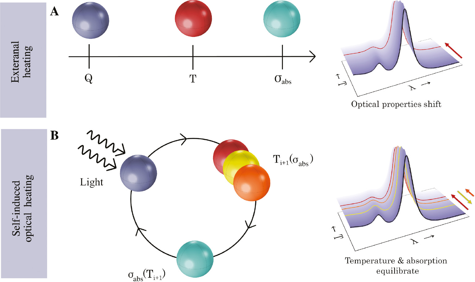
Conceptual representation of external heating and self-induced optical heating.
Externally triggered (A) and self-induced (B) thermo-optical effects on the shift of the optical properties of dielectric nanoresonators. Panel (B) visualizes our recursive method that calculates a new absorption cross-section spectrum at every new temperature reached until the temperature and absorption equilibrate under continuous wave illumination.
Contrary to external heating where temperature is an independently controlled parameter (Figure 1A), during self-induced optical heating temperature depends on the absorbed energy. This, in turn, strongly depends on the spectral characteristics of the resonators and hence its temperature (Figure 1B). The final steady-state condition is therefore determined by this recursive dependence between the absorbed energy and the resonator temperature. Under sufficiently intense irradiation, the resonance modes will be thus different in spectral position and amplitude from the desired ones, designed using room-temperature optical properties. This self-induced thermo-optical effect can have dramatic consequences in applications that employ high optical intensities such as Raman scattering [22], sensing [24], [25], and nonlinear optics [20]. Therefore, spectral shifts imposed by self-induced optical heating need to be quantitatively estimated.
In this work, we perform a detailed study of the processes and consequences of thermo-optical effects during self-induced optical heating of dielectric nanoresonators. We begin by developing a recursive analytical model to quantify spectral shifts and local temperatures in various Si spheres in air as a function of the mode utilized for resonant absorption. Importantly, we prove that self-heating induces notable spectral changes even for relatively low incident intensities (0.1–1 GW/m2). Our recursive method is then generalized with a numerical approach, applicable to any type of resonator and asymmetric environments. We are then able to confirm that self-heating significantly affects the optical response of Si spheres on a fused silica substrate. In particular, we demonstrate that an initially on-resonance illumination can result in a significantly off-resonance excitation at steady state, due to the self-induced thermo-optical shift of the mode. Finally, we apply our numerical approach to the technologically relevant case of anapole modes in Si and Ge nanodisks and show the nonlinear dependence of the spectral shifts of the anapole resonances with increasing light intensity. Overall, by demonstrating the importance of self-induced thermo-optical effects in dielectric resonators, our work will inform better design and performance optimization of dielectric-based nanosystems, from metalenses [43] to nanothermometers, unlocking their full technological potential.
2 Methods
2.1 Analytical methods
To analytically calculate the effect of self-heating for a Si dielectric nanosphere, we developed a recursive MATLAB (MathWorks Inc., Natick, MA, USA) code that combines the following:
The Mie solution for the optical spectrum of an arbitrary dielectric nanosphere is given in (1) through (12) [44].
(1)(2)(3)(4)where n is the refractive index of the dielectric sphere (we define a complex n=n′+n″, where n′ is the refractive index, and n″ is the absorption coefficient), and ns, the refractive index of the surrounding medium. The wave vector of the incoming plane electro-magnetic (EM) wave is defined as k, the diameter of the sphere as D, and the wavelength as λ0. Dimensionless parameters v and w are defined accordingly. The Riccati–Bessel functions ψψj and ξj seen in (5) and (6) are defined with the help of the Bessel functions of first (J) and second order (Y). J and Y are built-in MATLAB functions.
(5)(6)Using the ψ and ξ definitions, we are able to express the α and β Mie coefficients in a compact form:
(7)(8)Summing over the Mie coefficients for a number of iterations N, calculated by (9) [44],
(9)where v is given by (3), we are able to obtain the extinction, scattering and absorption cross sections of the sphere as seen in (10–12).
(10)(11)(12)The temperature profile of a self-heating sphere in a homogenous medium is expressed as [45]:
(13)
where ΔT is the resulting optically induced temperature difference,
Based on the above expressions, we implement a recursive analytical method to calculate the response to self-heating of a dielectric nanosphere made of a thermo-optical material (Si). We start from the MATLAB code given by Baffou [45]. This piece of code provides a vectorized calculation of the α and β Mie coefficients, utilizing the built-in Riccati–Bessel functions in the MATLAB programming environment. The order of the coefficients is determined by a condition based on the relative magnitudes of the sphere radius r=D/2 and the wave vector k. We sweep this Mie solution over a range of wavelengths, λ, and sphere diameters, D. We then sweep over the temperature range of the bibliographically available data [46]. This results in a wavelength, temperature- and size-dependent absorption cross-section matrix, σabs(λ, T, D). For a given sphere diameter and a monochromatic illumination, we extract the corresponding σabs(λ, Troom), and then we calculate the expected increase in temperature, ΔT, and hence the new temperature of the system, Ti=Troom+ΔT. If the material were not thermo-optical, this would be the final temperature of our system. However, in the case of a thermo-optical material, it is necessary to determine the new σabs(λ, Ti)≠σabs(λ, Troom). A change in the amount of absorbed light consequently leads to a different temperature, Ti+1=Ti+ΔT. This calculation must be recursively implemented until the values of σabs(λ, TN–1) and σabs(λ, TN) are identical (within a provided code definition tolerance). Overall, this method simulates the thermo-optical response of a dielectric nanosphere under continuous wave illumination. The full MATLAB code used is given in the supporting information.
With this code, we investigate two separate aspects. On the one hand, we calculate the temperature change ΔΤ of the dielectric nanosphere as a function of the intensity of the incident light Ι. During this calculation, the code also outputs the absorption, scattering, or extinction cross-section spectra at every step. On the other hand, we use the code to automatically identify the magnetic and electric dipole in the nanosphere absorption spectrum, and we track their shift as a function of the temperature change, due to increasing values of the light intensity. The possibility of identifying also the electric (EQ) and magnetic quadrupoles (MQ) is also included in the code.
2.2 Numerical methods
In order to numerically solve for the optical properties of any given shape, size, and dielectric character of a thermo-optically sensitive nanoresonator, as well as for asymmetric environments (e.g. resonator on a substrate), we use a multiphysics finite element software (COMSOL Inc., Burlington, MA, USA), solving for both the EM and heat transfer equations. We first determine the optical response of the nanoresonator on a substrate. Then we couple the EM solution to the heat-transfer part to determine the temperature reached under illumination. Similarly to the analytical case, we then update the optical properties and compute again the EM solution. We iterate until no further change is observed in temperature between two subsequent calculations.
To calculate for the optical properties of the nanoresonator on the substrate, we assume a linearly polarized electric field incident on a substrate where the nanoresonator is deposited (interface between the substrate and the resonator coincides with z=0). We introduce the incident, reflected, and transmitted waves, assuming normal incidence on the substrate, as seen in (14) for the geometrical domains on top and inside the substrate.
where E0 is the incident electric field amplitude, and rs and ts are the Fresnel coefficients for normal incidence [47]. We then solve the time-averaged wave equation for all the domains assigned with frequency-dependent dielectric properties as seen in (15). Fresnel coefficients rs and ts are updated for every wavelength solved.
The magnetic permeability is set to zero, μr=1, in all domains, whereas for the nanoresonator, we introduce the frequency- and temperature-dependent relative electric permittivity εr (f, T) [46], [48]. Applying a nonscattering boundary condition and a fully absorbing layer surrounding the finely meshed domains, we secure that the electric field solution is not affected by local artifact features and can be generalized for a number of noninteracting nanoresonators.
From the obtained electric field solution, we integrate for the energy rates absorbed and scattered by the nanoresonator volume and surface area, respectively, as found in (16).
By dividing each with the incident irradiance (17), we finally obtain the absorption and scattering cross sections (18).
From the tridimensional electric field solution and using the exact same geometrical configuration, domains, and meshing properties, we calculate the total dissipated optical heat on the nanoresonator in the presence of the substrate according to (19).
Based on each material thermal capacity (Cp), thermal conductivity (k), and density (ρ) [49], we solve for a steady-state heat transfer equation as seen in (20).
We apply a T=T0 boundary condition on the outer layer of the computational domain. We optimize the size of this boundary by test modeling of well-known systems from bibliography [50], [51].
Finally, we obtain the equilibrium temperature of the system. We average it over the volume of the nanoresonators, update the optical properties according to the εr (f, T) tables, and repeat for both the EM part and the heat transfer one.
3 Results and discussion
3.1 An analytical method for self-induced optical heating of a dielectric nanosphere
The type (electric or magnetic), order (dipole, quadrupole, etc.), and spectral position (wavelength) of the resonant modes that characterize the absorption, scattering, and extinction spectrum of a dielectric nanosphere are strongly dependent on its size. When the constituent material exhibits a significant thermo-optical effect, the characteristic wavelength and amplitude of these modes will also change, depending on the temperature (Supplementary Information Figure S3). As shown in Figure 2A–C, when heat is provided externally, a defined change in temperature can be arbitrarily imposed, and a corresponding shift in the optical response of a sphere will be observed due to thermo-optical effects. As an example, in the case of a Si sphere with diameter of 103 nm, heating from room temperature to 430 K will result in a 15-nm shift of the prominent magnetic dipole (MD) resonance. As indicated by (13) between the heat provided externally and the increase in temperature of the sphere, there is a linear dependence (Figure 2C).
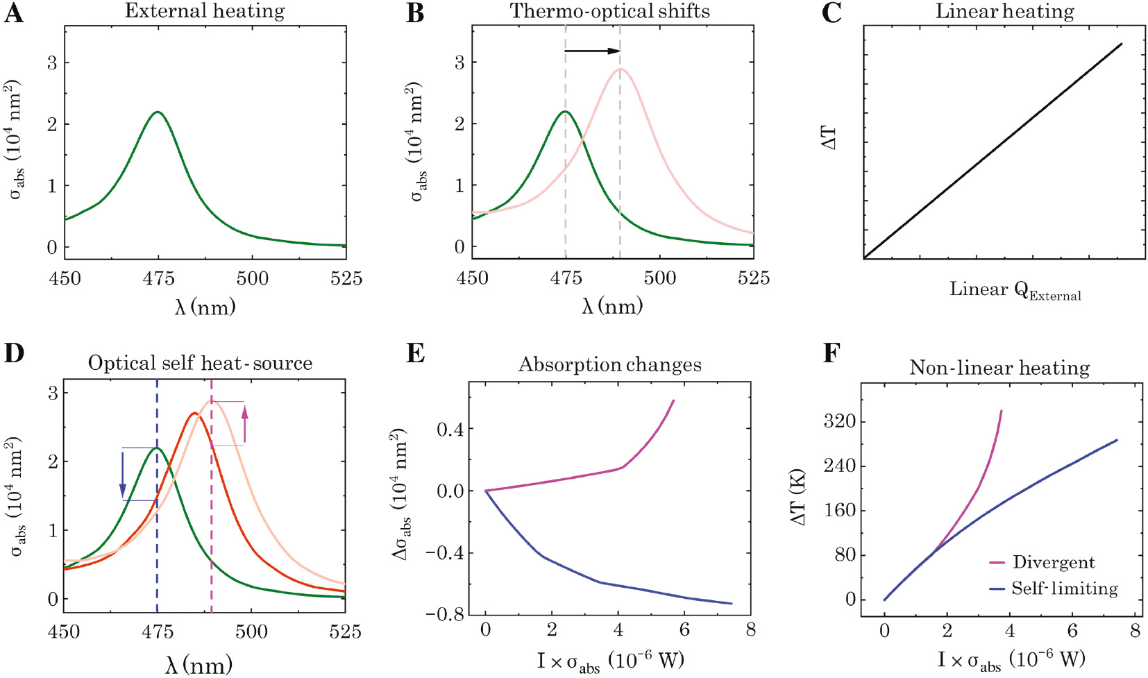
Relationship between optical properties and heating.
(A, B) Redshift of the MD mode peak position of a 103-nm Si nanosphere with temperature upon external heating. (C) Linear proportionality of the provided energy input and the temperature increase. (D) Redshift of the MD mode peak position with temperature upon illumination with 475 nm (blue line). Initially, on-resonance illumination (blue line on green spectrum) becomes off-resonance (red spectrum) as the temperature increases, determining a reduction of the input energy. Initially off-resonance illumination with 490 nm (pink line on red spectrum) can become on-resonance (dashed line on beige spectrum) with a significant increase of the input energy. (E) Shift of the absorption cross section (Δσabs) with input intensity for 475-nm illumination (initially on resonance that gradually becomes off resonance, blue line) and for 490-nm illumination (initially off resonance that gradually becomes on resonance, pink line). (F) Initially on-resonance illumination thus results in a self-limiting heating as a function of the effective absorbed power (blue line), whereas off-resonance illumination results in a divergent heating (pink line).
On the other hand, when a sphere is illuminated with intense light, the thermo-optical effect depends on the self-induced optical heating, and hence the shift in the σabs spectrum of the sphere will depend on the equilibration between the varying absorbed power and the changing temperature, as graphically presented in Figure 1B. Considering again a sphere of 103-nm diameter, in the case of monochromatic light excitation with λ=λMD (Troom) (Figure 2D, green curve and blue line), we observe that the resonance redshifts as the particle heats up (Figure 2D, red and yellow curves). As a result, at equilibrium, the absorption will be lower than at room temperature. This gradually changing absorption is plotted in Figure 2E for a case of an on-resonance illumination that gradually becomes off-resonance and vice versa due to the self-induced heating and the concomitant absorption shifts. The increase in temperature with respect to the effective absorbed power at room temperature (σabs (λ, Troom)×I) will be thus sublinear, resulting in an apparent self-limiting heating behavior (Figure 2E, blue curve). In the case of monochromatic light excitation slightly on the right of the resonance [λ> λMD(Troom) Figure 2D, dashed pink line], instead, as the particle heats up, the absorption increases, due to the same redshifts of the resonance mode with temperature. As a result, the temperature increases faster than expected based on the designed absorbed power, and a divergent heating behavior can be observed (Figure 2E, pink curve). Overall, due to the optothermally induced shifts of the resonant modes, initially off-resonance monochromatic excitation can become on-resonant and vice versa. As a result, upon increasing the intensity of the incident radiation, temperature changes are not necessarily linearly dependent on it, both super- and sublinear behaviors being possible. This complex dependence of excitation power and local temperature entails that self-induced optical heating must be precisely assessed in order to unlock its full potential in applications ranging from sensing to tunable metasurfaces.
To gain deeper insight into the complex interaction of thermo-optical effects with the resonant modes of the dielectric nanoantennas during self-induced optical heating, we use our analytical model to study the temperature evolution of three Si nanospheres as a function of light intensity for different monochromatic illuminations (Figure 3). We specifically choose three sizes that exhibit different relative amplitudes of the ED and MD modes in the absorption spectrum. Note that, as discussed in Figure S10 in the SI, the relative intensities of the absorption peaks do not follow the trends observed in the scattering ones. For 80-nm diameter, the MD mode is dominant; for 103-nm diameter, the MD and ED modes have the same magnitude, and for 130-nm diameter, the ED mode is dominant. We then assess how the temperature changes during monochromatic illumination with increasing intensity, both on- and off-resonance, across all the resonant modes. We note that for strong and sharp resonant modes (e.g. MD for 80 nm, both ED and MD for 103 nm, and ED for 130 nm) on-resonant excitation leads to a self-limiting dependence of the ΔT on the effective absorbed power, as expected from our previous discussion. Instead, the significantly weaker EQ and MQ modes (within the 80- to 130-nm Si sphere diameter regime) exhibit an almost linear dependence of the ΔT on the equivalent absorbed power, analogous to external heating. Hence, the strong resonances excited in dielectric resonators are critical to observe the unique trends in ΔT during self-induced optical heating. Finally, we observe that off-resonance excitation, both for λexcitation>λresonance and for λexcitation<λresonance, leads to a divergent trend in ΔT. These rules apply consistently to resonance modes with peak wavelength shorter than 500 nm. Instead, in the case of the 130-nm Si sphere, both the MD and the local minimum at 500 nm exhibit a fluctuating behavior that shifts between self-limiting and divergent to the end of the available temperature-dependent dielectric data for Si [46]. To understand this behavior, it is necessary to consider the temperature dependence of the absorption cross section for each of these spheres (Supplementary Information Figure S1). When a resonance occurs at wavelengths shorter than 475 nm, it redshifts, broadens, and decreases in intensity and as temperature rises. Resonance peaks around 450 nm redshift and broaden but do not change in intensity as temperature rises. Modes at wavelengths longer than 475 nm also redshift and broaden, but they uniquely increase in intensity as temperature rises. Therefore, in this wavelength range, the increases in intensity of the resonance counteract the lower absorbed power caused by the redshift of the peak, resulting in the fluctuating behavior seen in the magenta and the gray lines in Figure 3F.
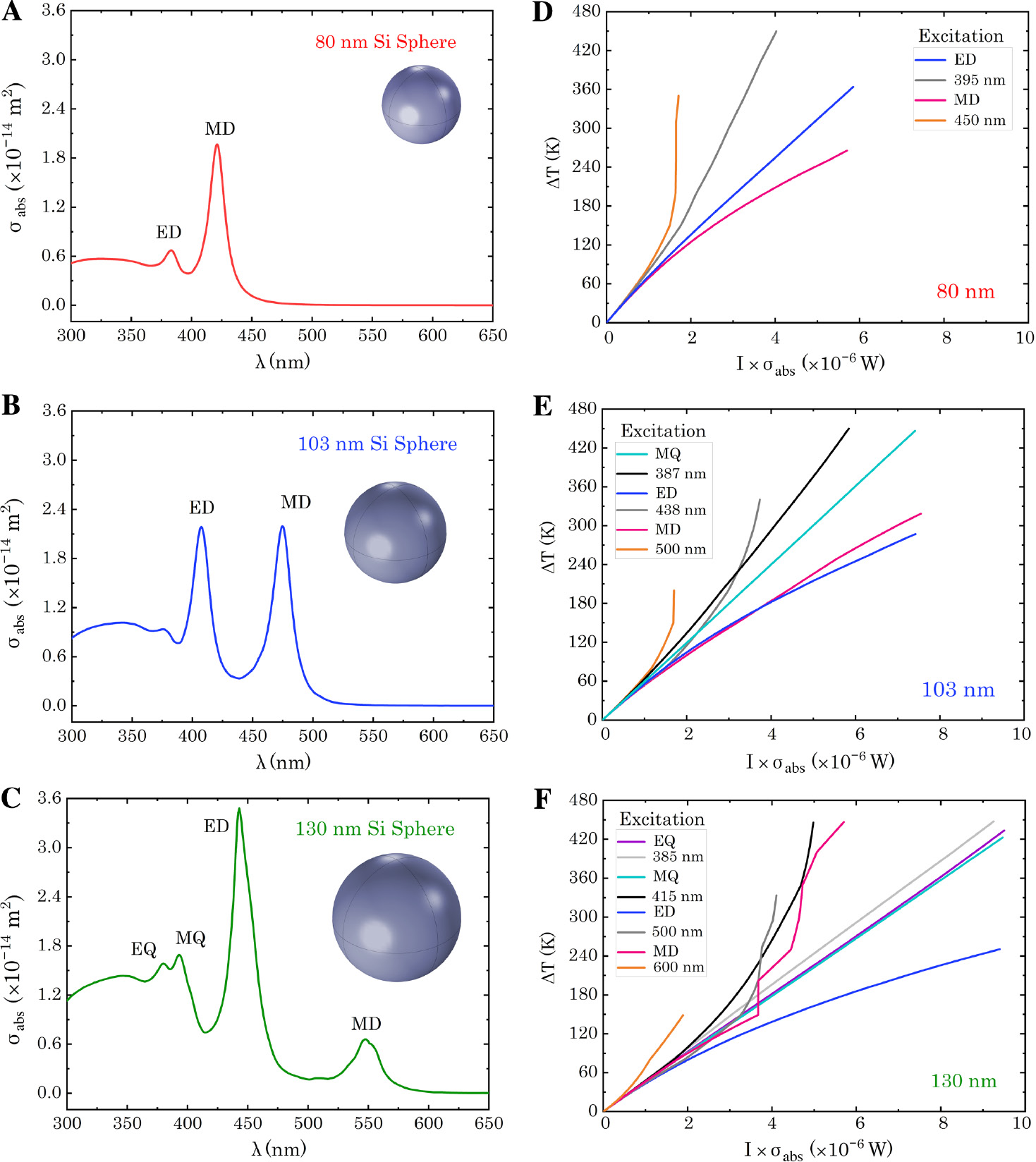
Analytical analysis of self-induced heating of Si nanospheres.
(A–C) Absorption cross section at room temperature of three Si spheres with diameters of 80-, 103-, and 130-nm Si sphere; (D–F) temperature increase observed upon illumination at the indicated on- or off-resonance wavelengths as a function of the effective absorbed power. Self-limiting, linear, divergent, and fluctuating behaviors are observed, illustrating the complexity of self-induced optical heating.
We have so far analyzed the patterns of self-induced optical heating of the particle while illuminating on and off the most prominent resonant modes. However, this does not yet describe how these modes shift during illumination. The complex coupling between the self-induced optical heating and the thermo-optical effects is indeed reflected in the shift of each resonance wavelength, Δλ, as a function of the average increase in temperature of the nanoparticle, ΔT. For systems with no significant absorption, this shift can be adequately predicted by the temperature dependence of the thermo-optical coefficient, which encapsulates the shift in the refractive index of a material with respect to the changing material temperature [52], [53], [54]. In self-induced optothermal heating, however, one has to account for the change in both the real and the imaginary part of the dielectric function with temperature (see Supplementary Information Figure S4). Following recent literature [55], we thus define the self-induced thermo-optical shift for each mode and illumination condition by measuring Δλ with respect to ΔT. We note that at these frequencies the complex refractive index has a nonnegligible dispersion. Therefore, as discussed above for the ΔT (I·σabs), the self-induced thermo-optical shift of a mode strongly depends on the illumination wavelength.
With our MATLAB code, we indeed track the shift of the four fundamental resonant modes of Si spheres (MD, ED, MQ, and EQ) for excitation at different illumination wavelengths. In particular, in Figure 4, we compare the spectral shifts of the MD and ED modes of Si spheres with diameters of 80, 103, 130, and 140 nm, during on-resonance illumination for each mode [λ= λMD(D) or λ= λED(D)]. We do that for both the scattering and the absorption peaks while illuminating at the ED and MD modes of the absorption. Our code allows for one to design their dielectric nanoresonator application by tracking any of the four modes under any illumination. In Figure 4, we observe that, in most cases, the self-induced thermo-optical shifts (Δλ/ΔT) present two linear dependences with decreasing slopes, below and above ΔT~50 K. Furthermore, up to ΔT=350 K, most curves appear to be almost linear for both scattering and absorption peak tracking. Uniquely, the Δλ/ΔT of the MD mode for the 130- and 140-nm Si spheres increases linearly within a small ΔT range and then fluctuates to the end of the available data. This behavior reflects the previous discussion on the increase in intensity of the resonant modes with peak wavelength longer than 475 nm. We thus conclude that the larger the temperature increase and the sphere radius, the more fluctuating and nonlinear the self-induced thermo-optical shifts become.
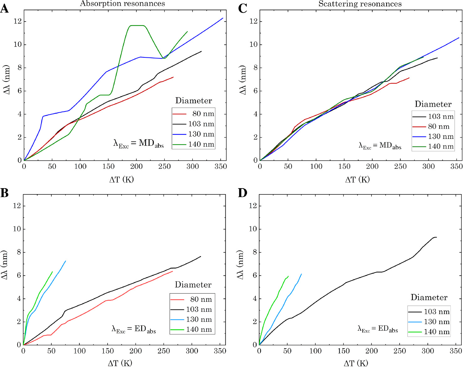
Self-Induced thermo-optical shifts of the magnetic dipole (MD) and the electric dipole (ED) resonances of silicon nanospheres of increasing radii.
In (A) and (B), we track the shifts of the MD and ED modes for λ=MD and λ=ED on-resonance illuminations for the absorption cross-section peaks. In (C) and (D), we track the resonant shifts of the MD and ED modes of the scattering cross-section spectra when illuminating at the MD and ED of the absorption. As seen in Figure S10, the MD mode maxima appear at almost the same wavelengths for scattering and absorption, whereas the ED mode has few nanometer shifts. The behavior changes from almost linear at smaller radii to nonlinear and fluctuating as the size increases, especially for the MD resonance of the absorption.
Overall, with our simple analytical approach, we showed that, when a Si nanosphere system is illuminated with intensity I>0.5 GW/m2, or equivalently, it absorbs more than ~1 μW, it is critical to account for the self-induced optical heating for the design of the resonator. Furthermore, we observed that self-induced heating results in significant, nonlinear spectral shifts of the resonant modes as a function of the effective absorbed power. Although this approach is computationally efficient, its applicability is limited to simple geometries – sphere – and homogeneous environments. Therefore, we used a numerical approach to extend the analysis to more complex geometries.
3.2 A numerical method for self-induced optical heating of any dielectric nanoresonator on any substrate
For dielectric nanoresonators of increasing anisotropy, either from a shape or an environment perspective, we have developed a numerical method using the commercially available software COMSOL multiphysics as described in the Methods section. This recursive method calculates numerically for the optical properties of an arbitrary nanoresonator. The heat generated by the optical losses in the nanoresonator’s volume is then used to calculate for the temperature rise in both the nanoresonator and its environment. We average the temperature on the nanoresonator and apply the respective shift in the dielectric properties and repeat from step 1 (Figure 5A). Figure 5B shows the self-induced thermo-optical effect for a 350-nm Si sphere on a fused silica substrate. We choose this nanoresonator because it exhibits a strong MQ resonance at 631 nm, close to the fundamental emission line of a helium–neon laser at ~633 nm, which we assume as our light source. Initial illumination is thus redshifted compared to the designed resonance mode (Figure 5B, black and red lines). However, upon excitation with I=2 GW/m2, the temperature increases dramatically due to self-induced optical heating and hence redshifts the mode until the excitation wavelength becomes blueshifted (peak resonance ~640 nm at ~575 K; Figure 5B, C). At this point, because of the significantly reduced absorption cross section (Figure 5B, light gray curve), the system cools down, and the resonance shifts back, eventually setting on an equilibrium temperature that balances the optothermal energy input with the nanoresonator temperature. Strikingly, we observe that while by design we aimed at illuminating on the right of the resonance, at equilibrium the illumination is blueshifted compared to the resonance peak, which has shifted by ~4 nm. With this realistic case, we show that even with an intensity of 2 GW/m2 (or the equivalent of a 20-μW absorbed power) we experience a notable shift. Also, we observe that, although our calculations are performed as a series of sequential equilibrium states, in reality during the heating phase the system must be rapidly fluctuating on and off resonance. Interesting questions thus emerge regarding the time scale of the heating phenomena and the thermo-optical dynamics that can be observed as a consequence of it, which will be the subject of future studies. Overall, this realistic example further confirms the importance of carefully accounting for thermo-optical effects during the design phase of dielectric nanoresonators.
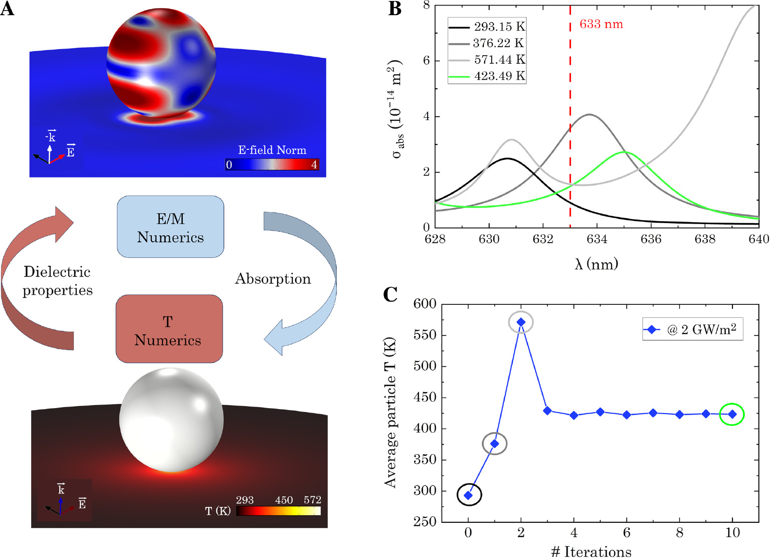
Recursive numerical modeling of self-induced optical heating.
(A) Schematic illustration of the recursive numerical calculation that continuously iterates between electromagnetic and thermal calculations, updating the absorbed power and dielectric properties accordingly. (B) Absorption cross-section spectrum of a Si nanosphere of 350-nm diameter on a fused silica substrate as a function of temperature for different steps of the iterative procedure. The black line represents the initial situation at room temperature, whereas the green line is the spectrum at equilibrium. The red line is the chosen illumination wavelength. (C) Average temperature of the nanosphere as a function of the iteration step.
3.3 Self-induced optothermal heating of anapole nanoresonators
Given the prominent technological relevance of anapole modes in resonators, we analyze the self-induced thermo-optical effect in two commonly studied systems: a 50-nm-thick Si nanodisk with a diameter of 200 nm [5], [15] and a 100-nm-thick Ge nanodisk with a diameter of 500 nm [20]. As discussed in the introduction, anapole modes are very appealing because they exhibit a strong minimum in scattering. However, we note that such resonators also exhibit a pronounced absorption peak at approximately the same wavelength as the anapole scattering dip (Figure S5). As recently shown, nanodisk metasurface properties can be thermally tuned with externally provided heat [40], [56]. Indeed, both Si and Ge anapole nanodisks resonances shift linearly with externally provided heat (Figure S6 and S7). However, based on our previous analysis, we expect the self-induced optical heating to result in a more complex behavior.
We use our numerical recursive approach to determine the equilibration temperature (Figure 6A, B) and scattering spectra (Figure 6C, D) of the Si and Ge nanodisks as a function of light intensity for excitation at the room temperature anapole scattering minimum (Figure 6C, D, black curves). As seen in Figure 6B and D, Ge anapoles are very sensitive to self-induced optical heating: a 4-GW/m2 illumination intensity induces a ΔT of ~200 K and a Δλ of 80 nm, while a 12 GW/m2 causes a ΔT of ~550 K and a Δλ of 110 nm. Silicon anapoles are less sensitive to the incoming intensity, but they still experience nonnegligible optical shifts (~20-nm shift for a 24-GW/m2 intensity). As a term of comparison, this intensity is roughly one-fifth of the optical intensities used for Raman scattering and 1000 less than the ones used for nonlinear optical applications such as third-harmonic generation (Figure S9). While compensation of thermo-optical effects is routinely performed in nonlinear optics experiments, these results show that they should be taken carefully into account also for less intense illumination conditions. Finally, when tracing the shift of the anapole mode dip as a function of illumination intensity, we observe that the trends are far from linear. In particular, while Si nanodisks exhibit two different linear regimes, Ge nanodisks exhibit a nonmonotonic redshift of the mode (Figure 5E, F). Our study was limited by the available temperature range for the dielectric properties of Si and Ge, but it is expected that further shifts and other nontrivial trends might occur for even higher intensity. Therefore, self-induced optical heating must be carefully assessed prior to employing these resonators in sensing applications where the shift in the resonance-mode dip is utilized to determine local events. In fact, even in the presence of a substrate and for moderate illumination intensities, heating can be sufficient to significantly shift the mode, with nontrivial dependence on the intensity.
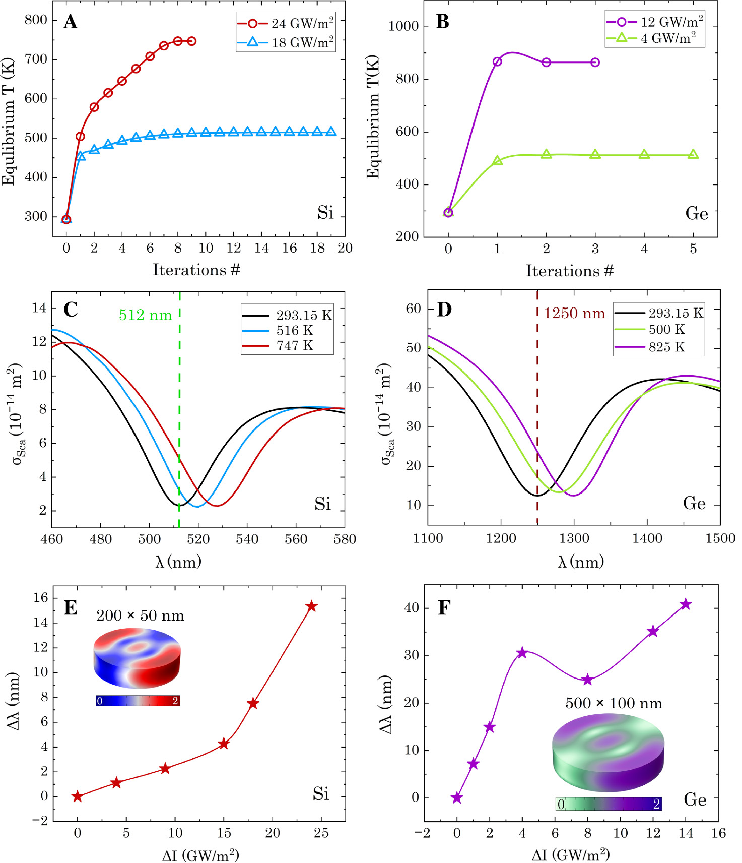
Self-induced optical heating of Si and Ge nanodisks supporting anapole modes.
(A, B) Evolution of the average temperature of the nanodisks as a function of the iteration until equilibrium, for different illumination intensities; (C, D) scattering cross-section spectrum of the Si and Ge nanodisks exhibiting an anapole dip. Black curves are the room temperature spectra, whereas the colored curves represent the shift of the anapole mode due to self-induced optical heating, resulting in the indicated equilibrium temperature. The used illumination is shown in (A) and (B). The green and red vertical lines indicate the respective excitation wavelengths. (E, F) Spectral shift of the anapole mode as a function of the illumination intensity. The respective illumination wavelengths are shown in (C) and (D). Complex nonlinear behaviors are observed for self-induced optical heating of these resonators.
4 Conclusions
In summary, in this work, we have discussed the importance of self-induced optical heating in dielectric nanoresonators made of materials (Si and Ge) that exhibit strong thermo-optical effects. We have provided both an analytical and a numerical method that recursively solve the EM and thermal aspects of the problem, ultimately accounting for the complex interaction between them. We used both approaches to showcase the significant impact of self-induced optical heating onto the equilibrium temperature of Si nanospheres. In particular, we observed that, contrary to self-heating, with this approach it is possible to design systems with self-limiting or divergent thermal behaviors. Further optimization could thus enable the design of optical heaters that can be robust against fluctuations of the light source or optical sensors for rapid detection of changes in the source intensity. Finally, we demonstrated the importance of assessing self-induced optical heating in applications that exploit anapole nanoresonators, one of the most successful and interesting dielectric systems. In fact, even at mild intensities, relevant for sensing or Raman applications, these resonators can absorb significant amounts of energy resulting in a prominent shift of the mode, with nonlinear dependence on the illumination intensities. Moving forward, we foresee interesting opportunities in the understanding of the time evolution of these effects at fast time scales. This work employs a steady-state approach on the self-induced thermal effects of known and widely used systems in the visible and in the infrared. We are currently focusing on anomalous thermo-optic effects that shift the resonances in both directions and/or change their behavior with intensity and resonant wavelength.
Overall, our work highlights the necessity of assessing the self-induced optical heating in a wider range of thermo-optically sensitive materials. The universality of the used analytical and numerical methods provides a widely applicable platform. We hence expect that this work will have a momentous impact in the fields of dielectric and plasmonic nanoresonators, dielectric metasurfaces and metamaterials, and anapole resonator systems by stimulating further investigation and debate on the potential of self-induced thermo-optical effects.
References
[1] Kuznetsov AI, Miroshnichenko AE, Brongersma ML, Kivshar YS, Luk’yanchuk B. Optically resonant dielectric nanostructures. Science 2016;354:aag2472.10.1126/science.aag2472Search in Google Scholar PubMed
[2] Kim SJ, Fan P, Kang JH, Brongersma ML. Creating semiconductor metafilms with designer absorption spectra. Nat Commun 2015;6:7591.10.1038/ncomms8591Search in Google Scholar PubMed PubMed Central
[3] Yavas O, Svedendahl M, Dobosz P, Sanz V, Quidant R. On-a-chip biosensing based on all-dielectric nanoresonators. Nano Lett 2017;17:4421–6.10.1021/acs.nanolett.7b01518Search in Google Scholar PubMed
[4] Chang Y, Hasan D, Dong B, et al. All-dielectric surface-enhanced infrared absorption-based gas sensor using guided resonance. ACS Appl Mater Interfaces 2018;10:38272–9.10.1021/acsami.8b16623Search in Google Scholar PubMed
[5] Staude I, Miroshnichenko AE, Decker M, et al. Tailoring directional scattering through magnetic and electric resonances in subwavelength silicon nanodisks. ACS Nano 2013;7:7824–32.10.1021/nn402736fSearch in Google Scholar PubMed
[6] Bakker RM, Permyakov D, Yu YF, et al. Magnetic and electric hotspots with silicon nanodimers. Nano Lett 2015;15:2137–42.10.1021/acs.nanolett.5b00128Search in Google Scholar PubMed
[7] Yang Y, Miller OD, Christensen T, Joannopoulos JD, Soljačić M. Low-loss plasmonic dielectric nanoresonators. Nano Lett 2017;17:3238–45.10.1021/acs.nanolett.7b00852Search in Google Scholar PubMed
[8] Decker M, Pertsch T, Staude I. Strong coupling in hybrid metal–dielectric nanoresonators. Philos Trans A Math Phys Eng Sci 2017;375:20160312.10.1098/rsta.2016.0312Search in Google Scholar PubMed PubMed Central
[9] Tuz VR, Khardikov VV, Kupriianov AS. High-quality trapped modes in all-dielectric metamaterials. Opt Express 2018;26:2905–16.10.1364/OE.26.002905Search in Google Scholar PubMed
[10] Sell D, Yang J, Doshay S, Fan JA. Periodic dielectric metasurfaces with high-efficiency, multiwavelength functionalities. Adv Opt Mater 2017;5:1700645.10.1002/adom.201700645Search in Google Scholar
[11] Zhou J, Qian H, Chen CF, et al. Optical edge detection based on high-efficiency dielectric metasurface. PNAS 2019;116:11137–40.10.1073/pnas.1820636116Search in Google Scholar PubMed PubMed Central
[12] Overvig AC, Shrestha S, Malek SC, et al. Dielectric metasurfaces for complete and independent control of the optical amplitude and phase. Light Sci Appl 2019;8:92.10.1038/s41377-019-0201-7Search in Google Scholar PubMed PubMed Central
[13] Kaelberer T, Fedotov VA, Papasimakis N, Tsai DP, Zheludev NI. Toroidal dipolar response in a metamaterial. Science 2010;330:1510–2.10.1126/science.1197172Search in Google Scholar PubMed
[14] Savinov V, Papasimakis N, Tsai DP, Zheludev NI. Optical anapoles. Commun Phys 2019;2:69.10.1038/s42005-019-0167-zSearch in Google Scholar
[15] Yang Y, Zenin VA, Bozhevolnyi SI. Anapole-assisted strong field enhancement in individual all-dielectric nanostructures. ACS Photonics 2018;5:1960–6.10.1021/acsphotonics.7b01440Search in Google Scholar
[16] Miroshnichenko AE, Evlyukhin AB, Yu YF, et al. Nonradiating anapole modes in dielectric nanoparticles. Nat Commun 2015;6:8069.10.1038/ncomms9069Search in Google Scholar PubMed PubMed Central
[17] Koshelev K, Favraud G, Bogdanov A, Kivshar Y, Fratalocchi A. Nonradiating photonics with resonant dielectric nanostructures. Nanophotonics 2019;8:725.10.1515/nanoph-2019-0024Search in Google Scholar
[18] Shcherbakov MR, Neshev DN, Hopkins B, et al. Enhanced third-harmonic generation in silicon nanoparticles driven by magnetic response. Nano Lett 2014;14:6488–92.10.1021/nl503029jSearch in Google Scholar PubMed
[19] Xu L, Rahmani M, Zangeneh Kamali K, et al. Boosting third-harmonic generation by a mirror-enhanced anapole resonator. Light Sci Appl 2018;7:44.10.1038/s41377-018-0051-8Search in Google Scholar PubMed PubMed Central
[20] Grinblat G, Li Y, Nielsen MP, Oulton RF, Maier SA. Enhanced third harmonic generation in single germanium nanodisks excited at the anapole mode. Nano Lett 2016;16:4635–40.10.1021/acs.nanolett.6b01958Search in Google Scholar PubMed
[21] Grinblat G, Li Y, Nielsen MP, Oulton RF, Maier SA. Efficient third harmonic generation and nonlinear subwavelength imaging at a higher-order anapole mode in a single germanium nanodisk. ACS Nano 2017;11:953–60.10.1021/acsnano.6b07568Search in Google Scholar PubMed
[22] Baranov DG, Verre R, Karpinski P, Käll M. Anapole-enhanced intrinsic Raman scattering from silicon nanodisks. ACS Photonics 2018;5:2730–6.10.1021/acsphotonics.8b00480Search in Google Scholar
[23] Yang C-Y, Yang J-H, Yang Z-Y, et al. Nonradiating silicon nanoantenna metasurfaces as narrowband absorbers. ACS Photonics 2018;5:2596–601.10.1021/acsphotonics.7b01186Search in Google Scholar
[24] Algorri FJ, Zografopoulos CD, Ferraro A, et al. Anapole modes in hollow nanocuboid dielectric metasurfaces for refractometric sensing. Nanomaterials 2018;9.10.3390/nano9010030Search in Google Scholar PubMed PubMed Central
[25] Sabri L, Huang Q, Liu J-N, Cunningham BT. Design of anapole mode electromagnetic field enhancement structures for biosensing applications. Opt Express 2019;27:7196–212.10.1364/OE.27.007196Search in Google Scholar PubMed
[26] Baranov DG, Zuev DA, Lepeshov SI, et al. All-dielectric nanophotonics: the quest for better materials and fabrication techniques. Optica 2017;4:814–25.10.1364/OPTICA.4.000814Search in Google Scholar
[27] Yi G-C. Semiconductor nanostructures for optoelectronic devices: processing, characterization and applications. Berlin Heidelberg, Springer – Verlag, 2012.10.1007/978-3-642-22480-5Search in Google Scholar
[28] Li Y, Qian F, Xiang J, Lieber CM. J. M. t., Nanowire electronic and optoelectronic devices. 2006;9:18–27.10.1016/S1369-7021(06)71650-9Search in Google Scholar
[29] Zhong H, Bai Z, Zou B. Tuning the luminescence properties of colloidal I–III–VI semiconductor nanocrystals for optoelectronics and biotechnology applications. J Phys Chem Lett 2012;3:3167–75.10.1021/jz301345xSearch in Google Scholar PubMed
[30] Joyce HJ, Gao Q, Hoe Tan H, et al. III–V semiconductor nanowires for optoelectronic device applications. Prog Quant Electron 2011;35:23–75.10.1016/j.pquantelec.2011.03.002Search in Google Scholar
[31] Emani NK, Khaidarov E, Paniagua-Domínguez R, et al. High-efficiency and low-loss gallium nitride dielectric metasurfaces for nanophotonics at visible wavelengths. Appl Phys Lett 2017;111:221101.10.1063/1.5007007Search in Google Scholar
[32] Krasilin AA, Zuev DA, Dyachuk VA, Milichko VA. Light induced heating of Ge nanoparticle covered by BSA. J Phys Conf Ser 2018;1092:012089.10.1088/1742-6596/1092/1/012089Search in Google Scholar
[33] Krasilin AA, Volodina K, Sukhova AA, et al. The conformation of bovine serum albumin adsorbed to the surface of single all-dielectric nanoparticles following light-induced heating. J Biophotonics 2018;11:e201700322.10.1002/jbio.201700322Search in Google Scholar PubMed
[34] Zograf GP, Timin AS, Muslimov, et al. All-optical nanoscale heating and thermometry with resonant dielectric nanoparticles for photoinduced tumor treatment. 2019;arXiv:1906.06150v1.10.1002/lpor.201900082Search in Google Scholar
[35] Mecklenburg M, Zutter B, Regan BC. Thermometry of silicon nanoparticles. Phys Rev Appl 2018;9:014005.10.1103/PhysRevApplied.9.014005Search in Google Scholar
[36] Zograf GP, Petrov MI, Zuev DA, et al. Resonant nonplasmonic nanoparticles for efficient temperature-feedback optical heating. Nano Lett 2017;17:2945–52.10.1021/acs.nanolett.7b00183Search in Google Scholar PubMed
[37] Huang S, Parimi VS, Deng S, Lingamneni S, Zheng X. Facile thermal and optical ignition of silicon nanoparticles and micron particles. Nano Lett 2017;17:5925–30.10.1021/acs.nanolett.7b01754Search in Google Scholar PubMed
[38] Staude I, Schilling J. Metamaterial-inspired silicon nanophotonics. Nat Photonics 2017;11:274–84.10.1038/nphoton.2017.39Search in Google Scholar
[39] Memon FA, Morichetti F, Melloni A. High thermo-optic coefficient of silicon oxycarbide photonic waveguides. ACS Photonics 2018;5:2755–9.10.1021/acsphotonics.8b00512Search in Google Scholar
[40] Lewi T, Butakov Nikita A, Schuller Jon A. Thermal tuning capabilities of semiconductor metasurface resonators. Nanophotonics 2019;8:331.10.1515/nanoph-2018-0178Search in Google Scholar
[41] Lewi T, Butakov NA, Iyer PP, et al. Reconfigurable semiconductor Mie-resonant meta-optics. SPIE 2019;11080.10.1117/12.2528259Search in Google Scholar
[42] Iyer PP, DeCrescent RA, Lewi T, Antonellis N, Schuller JA. Uniform thermo-optic tunability of dielectric metalenses. Phys Rev Appl 2018;10:044029.10.1103/PhysRevApplied.10.044029Search in Google Scholar
[43] Afridi A, Canet-Ferrer J, Philippet L, Osmond J, Berto P, Quidant R. Electrically driven varifocal silicon metalens. ACS Photonics 2018;5:4497–503.10.1021/acsphotonics.8b00948Search in Google Scholar
[44] Bohren CF, Huffman DR. Absorption and scattering of light by small particles. Hoboken, John Wiley & Sons, 1983.Search in Google Scholar
[45] Baffou G. Thermoplasmonics: heating metal nanoparticles using light. Cambridge: Cambridge University Press, 2017.10.1017/9781108289801Search in Google Scholar
[46] Vuye G, Fisson S, Nguyen Van V, Wang Y, Rivory J, Abelès F. Temperature dependence of the dielectric function of silicon using in situ spectroscopic ellipsometry. Thin Solid Films 1993;233:166–70.10.1016/0040-6090(93)90082-ZSearch in Google Scholar
[47] Papas CH. Theory of electromagnetic wave propagation. New York, McGraw-Hill, Inc., 1965.Search in Google Scholar
[48] Viña L, Logothetidis S, Cardona M. Temperature dependence of the dielectric function of germanium. Phys Rev B 1984;30:1979–91.10.1103/PhysRevB.30.1979Search in Google Scholar
[49] Valencia JJ, Quested PN. Thermophysical properties. In:Metals process simulation. Vol. 22B. Furrer DU, Semiatin SL, eds. Cleveland, ASM International, 2010:18–32.10.31399/asm.hb.v22b.a0005523Search in Google Scholar
[50] Baffou G, Berto P, Bermúdez Ureña E, et al. Photoinduced heating of nanoparticle arrays. ACS Nano 2013;7:6478–88.10.1021/nn401924nSearch in Google Scholar PubMed
[51] Baffou G, Quidant R. Thermo-plasmonics: using metallic nanostructures as nano-sources of heat. Laser Photonics Rev 2013;7:171–87.10.1002/lpor.201200003Search in Google Scholar
[52] Frey BJ, Leviton DB, Madison TJ. Temperature-dependent refractive index of silicon and germanium. In: Optomechanical technologies for astronomy. Orlando, Florida, United States, International Society for Optics and Photonics, SPIE Astronomical Telescopes + Instrumentation, 2006:62732J.10.1117/12.672850Search in Google Scholar
[53] Chapter 3–thermo-optic coefficients. In: Handbook of optical constants of solids. Palik ED, ed. Burlington, Academic Press, 1997:115–261.10.1016/B978-012544415-6.50150-3Search in Google Scholar
[54] Ghosh G. Temperature dispersion of refractive indices in crystalline and amorphous silicon. Appl Phys Lett 1995;66:3570–2.10.1063/1.113790Search in Google Scholar
[55] Trenti A, Borghi M, Biasi S, et al. Thermo-optic coefficient and nonlinear refractive index of silicon oxynitride waveguides. AIP Adv 2018;8:025311.1.10.1063/1.5018016Search in Google Scholar
[56] Sautter J, Staude I, Decker M, et al. Active tuning of all-dielectric metasurfaces. ACS Nano 2015;9:4308–15.10.1021/acsnano.5b00723Search in Google Scholar PubMed
Supplementary Material
The online version of this article offers supplementary material (https://doi.org/10.1515/nanoph-2019-0534).
© 2020 Giulia Tagliabue et al., published by De Gruyter, Boston/Berlin
This work is licensed under the Creative Commons Attribution 4.0 International License.
Articles in the same Issue
- Editorial
- Interdisciplinary nanophotonics
- Reviews
- Advances in exploiting the degrees of freedom in nanostructured metasurface design: from 1 to 3 to more
- On-chip nanophotonics and future challenges
- All-dielectric metasurfaces for polarization manipulation: principles and emerging applications
- Nonlinear nanophotonic devices in the ultraviolet to visible wavelength range
- Active plasmonic nanoantenna: an emerging toolbox from photonics to neuroscience
- Research Articles
- Simply synthesized nitrogen-doped graphene quantum dot (NGQD)-modified electrode for the ultrasensitive photoelectrochemical detection of dopamine
- Design and optimization of tunneling photodetectors based on graphene/Al2O3/silicon heterostructures
- Self-induced thermo-optical effects in silicon and germanium dielectric nanoresonators
- Plasmon-controlled, ultra-bright, excitation-polarization-independent photoluminescence from individual Ag nanoplates
- Passively Q-switched Yb-doped all-fiber laser based on Ag nanoplates as saturable absorber
- Stacking angle dependent multiple excitonic resonances in bilayer tungsten diselenide
- Optically and radio frequency (RF) transparent meta-glass
- Critical review of quantum plasmonic models for finite-size media
- Tunable plasmon-phonon polaritons in anisotropic 2D materials on hexagonal boron nitride
- Pixeled metasurface for multiwavelength detection of vitamin D
- Phase-controlled metasurface design via optimized genetic algorithm
- Superlattice nonlinearities for Gigahertz-Terahertz generation in harmonic multipliers
- Multipolar second-harmonic generation from high-Q quasi-BIC states in subwavelength resonators
- Lasing at the nanoscale: coherent emission of surface plasmons by an electrically driven nanolaser
- Perovskite nanowire lasers on low-refractive-index conductive substrate for high-Q and low-threshold operation
- A simple transfer-matrix model for metasurface multilayer systems
- Enhanced two-photon photoluminescence assisted by multi-resonant characteristics of a gold nanocylinder
- Nanoscale control of single molecule Förster resonance energy transfer by a scanning photonic nanoantenna
- Magnetic switching of Kerker scattering in spherical microresonators
- High-efficiency, large-area lattice light-sheet generation by dielectric metasurfaces