Coupling single emitters to quantum plasmonic circuits
-
Alexander Huck


Abstract
In recent years, the controlled coupling of single-photon emitters to propagating surface plasmons has been intensely studied, which is fueled by the prospect of a giant photonic nonlinearity on a nanoscaled platform. In this article, we will review the recent progress on coupling single emitters to nanowires towards the construction of a new platform for strong light-matter interaction. The control over such a platform might open new doors for quantum information processing and quantum sensing at the nanoscale and for the study of fundamental physics in the ultrastrong coupling regime.
1 Introduction
When directing a photon towards a single emitter [e.g. an atom, a quantum dot (QD), or a defect center], the probability that the photon being absorbed (or emitted in a single mode) is typically very low due to the small cross-section of the emitter [1]. By strongly focusing the photon, the absorption probability can be largely improved [2–4] particularly if the photon is radially polarized [5], but reaching high probabilities is highly challenging particularly if the emitter is inhomogeneously broadened [6]. Another common approach to enhance the photon-emitter interaction strength is to place the emitter inside a cavity in which the photon bounces back and forth several times, thereby increasing the probability for absorption [7]. This approach, which is related to the Purcell effect [8], however, can be only used for narrowband emitters and photons due to the small bandwidth of the cavity. Finally, strong absorption can be attained by placing the emitter at an optimal position in the confined field of the plasmonic mode propagating along a small waveguide made of metal. As a plasmon mode, the propagating eigenmode of a waveguide made of metal can be tightly confined to below the optical diffraction limit [9], and the waveguide acts as an ultrastrong lens that focuses the light down to a few nanometers in the transverse dimension. Due to this exceptionally strong focusing capability, the emitter can interact with the photon with an extraordinary strength and thus absorb the photon with unit probability or, equivalently, a photon emitted from the dipole can be directed into a single plasmonic mode of the wire with unit probability [10].
Surface plasmon polaritons are electromagnetic excitations of charge density waves at the interface between a conductor and a dielectric medium, and as mentioned above, they can be confined to transverse dimensions much smaller than what is possible with conventional optics [11, 12]. Applying Fermi’s golden rule to evaluate the interaction strength between a dipole transition and such a surface plasmon mode, the coupling strength g is found to scale with the local electric field per photon, E0(r0), which is higher when the field confinement increases [10]. About a decade ago, it was theoretically suggested that the resulting coupling rate to propagating surface plasmon modes, Γpl, can largely exceed the spontaneous emission rate to the radiation field, Γrad, and that nonradiative decay rates, Γnonrad, are negligible for the considered parameter space [10].1 For a schematic illustration of the system, as an example, we chose a nanowire plasmon waveguide, and the rates are illustrated in Figure 1. These findings stimulated an enormous interest and triggered experimental efforts in using surface plasmon modes for enhanced light-matter interaction and device applications. It is worth mentioning that propagating surface plasmons are different from localized surface plasmons. In contrast to localized plasmons, propagating plasmons are traveling in a well-defined direction as the real part of their wavevectors is nonzero. This basically means that the propagating plasmon can be guided through metallic circuits much like optical beams in photonic circuits. The difference between the photonic and plasmonic guiding, however, is that the transverse dimension of the latter guiding can go below the diffraction limit and thus interact strongly with single emitters. The vision is therefore to build arbitrarily complex plasmonic circuits with metallic waveguides in which the plasmons can strongly interact with emitters and thereby enable classical and quantum information processing with a very small footprint. In addition to information processing, a scalable plasmonic platform of strongly interacting emitters and photons might be a promising system for investigating out-of-equilibrium many-body physics.
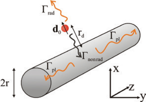
Schematic illustration of the individual decay channels of a dipole emitter d0 located at a distance rd next to a metallic nanowire. The emitter (orange sphere with black arrow) decays by emitting a single photon, which is directed into free space, into ohmic losses of the metallic wire, or into the single plasmonic mode propagating along wire. Γrad, Γpl, and Γnonrad denote the decay rates to the radiation field, the propagating surface plasmon mode, and the metallic loss channels, respectively. The ratio between the different rates is determined by the distance between the dipole emitter and the wire, rd.
In this review, we will describe experimental efforts towards the realization of an efficient interaction between a single optical dipole emitter and propagating surface plasmon modes supported by metallic waveguides. There exists a vast literature on plasmonics systems and circuits, which have been discussed in a number of review articles [12–17]. In this review, however, we mainly focus on quantum plasmonic circuits in which quantum states, and in particular single plasmonic states, are propagating. We thus focus on reviewing work on which single propagating plasmons are generated by a single emitter. We start by discussing the definition of “quantum plasmonics” and subsequently summarize different potential applications of the plasmon-emitter platform. Then, we discuss the various experimental activities solely focusing on the coupling between a “single emitter” and a propagating plasmon supported by a metallic waveguide. We conclude with an outlook in which we summarize a number of challenges that have to be solved for further progress and new directions of the field.
2 Quantum plasmonics
The property of strong confinement of the electromagnetic field has opened a new world of opportunities in both classical and quantum optics. Applications in the latter field have triggered the new field of quantum plasmonics [13]. But what is “quantum” in quantum plasmonics? Before answering this question, let us briefly review some of the first experiments carried out at the interface between quantum optics and plasmonics.
The experiment reported by Altewischer et al. [18] originally triggered the curiosity of the quantum optics community in the field of plasmonics. They have shown that the entanglement present in the polarization degree of freedom of two spatially separated optical modes survived after one of the photons passed through a gold film perforated with nanometer-sized holes. In the holes, photons excite surface plasmon resonances and thus enhance the total transmission through the gold film [19]. Later experiments reported by Fasel et al. [20] confirmed these findings by demonstrating that also time-energy entanglement was preserved after a photon-surface plasmon-photon conversion process. The survival of quadrature squeezing after surface plasmon excitation demonstrated that the phase coherence is also not affected by surface plasmon excitations [21, 22] and that linear propagation losses can be modeled by an effective beam splitter interaction. Together with the demonstration of Hong-Ou-Mandel interference of identical photons (produced externally by spontaneous parametric down-conversion) on a surface plasmon-based beam splitter [23–25], this series of experiments leaves little doubt that surface plasmon modes are well described by bosonic field operators.
These experiments suggest that plasmons behave similarly to bosonic electromagnetic fields. This is also what is expected from theory derived by Pines in the 1950s [26], establishing the quantization of collective electron oscillations that have bosonic properties. Due to the large number of electrons, a macroscopic collective excitation is formed and can be described by the macroscopic permittivity ∈ of the materials. This permittivity determines the mode profile and their guidance along a waveguide [9], and in a modern context, the quantization of surface plasmon modes has been addressed by Tame et al. [27], taking metal losses into account.
The aforementioned experiments are referred to as being “quantum plasmonics” experiments due to the fact that the statistics of the propagating plasmons cannot be described by a well-behaving Glauber-Sudharshan P-function. This function is defined as a weight function, P(α), in the coherent state basis |α〉, where α is the complex coherent state amplitude. The density matrix ρ̂ of a single mode state can then be written as ρ̂ = ∫ p(α)∣α〉〈α∣d2α [28, 29]. Quadrature squeezed states, single-photon states, and other non-Gaussian pure states do not possess a well behaving P-function and are thus often considered as nonclassical states. Therefore, the excitation of plasmonic modes in such nonclassical bosonic modes are often coined “quantum plasmonics” [13].
However, there exists also another definition of quantum plasmonics, which is relevant when the structures are reduced to very small dimensions of about a few nanometers. In this regime, the standard assumption of a continuous energy spectrum of the electrons might break down as the electrons become bounded and thus exhibit a quantized energy spectrum [30]. Furthermore, if very short length scales are considered, the quantum delocalization nature of electrons might be relevant and should be taken into account [31]. Due to this possible need for taking into account the energy quantization and the nonlocal nature of the electrons, the plasmonic behavior can only be described by a full quantum model; thus, it is referred to as “quantum plasmonics” [13]. However, all experiments to date on propagating plasmons have not been affected by these quantum phenomena (to the best of our knowledge); thus, the “quantum” in quantum plasmonics in previous experiments simply refers to the quantum statistics of the propagating bosonic mode. In addition to the entangled and squeezed plasmonic states discussed above, there have been a number of activities devoted to the generation of single plasmonic states by coupling single emitters to metallic waveguides. This will now be discussed in greater detail.
3 Emitter coupling to surface plasmons
In this section, we first consider the coupling of an emitter to a plasmonic mode supported by a metallic waveguide, as illustrated in Figure 1. The emitter with an angular transition frequency ω and dipole moment d0 is positioned a distance rd away from the surface of the waveguide. The one-dimensional waveguide is considered to have finite dimensions in the transverse (x, y)-plane and to be infinite in the longitudinal z-direction. The original framework for emitter-waveguide mode coupling was set by Klimov and Ducloy [32]. Using the quasi-static approximation, they derived an analytical expressions for the spontaneous emission rate into the guided mode, Γpl, radiation field, Γrad, and nonradiative emission due to dissipation of the fiber, Γnonrad, which is related to the imaginary part of the permittivity, 𝔍𝔪(∈). This work was later extended by Chang et al. [10] on the case of metallic nanowires supporting propagating surface plasmon modes [9]. It was found that, for an optimal dipole orientation parallel to the electric field component of the radially polarized surface plasmon mode, d0||Er, the decay rate into the plasmon mode Γpl (the guided mode in the dielectric nanofiber case) can largely exceed the sum of all other decay channels, i.e. Γpl≫Γrad+Γnonrad. This results in a β-factor very close to 1, where the β-factor is defined as the ratio of emission going into the guided modes to the total decay rate, β = Γpl/(Γpl+Γrad+Γnonrad). This result is the central motivation for the experimental investigations discussed in the following sections. The strong Γpl component, relative to all other decay channels, effectively originates from the tight mode confinement associated with the fundamental surface plasmon mode. For small rd, the Γnonrad component dominates, as it scales with
If the plasmon mode cannot be described analytically, for example, when the nanowire is placed on a substrate or in the case of other waveguides, such as grooves or wedges, the total decay rate Γtot and the individual decay channels (Γpl, Γnonrad, and Γrad) can only be obtained numerically using a finite-element method [33] or a finite difference time domain method [34]. Although, for the normalized plasmonic decay channel Γpl/Γ0, it is sufficient to know the electric E(x,y) and magnetic H(x,y) field distributions in the transverse (x,y)-plane, a rigorous modeling in three dimensions is required to obtain the total decay rate Γtot and to estimate the β-factor.
One may also obtain the decay rate of a dipole emitter at a position r using the proportionality Γ(r)∝𝔍𝔪TrG(r,r), where G(r,r) is the three-dimensional Green’s tensor [35]. In the vicinity to a two-dimensional, infinitely long waveguide with arbitrary shape, G(r,r), can be expressed in a Fourier series of two-dimensional Green’s tensors G2D(r∥,r∥,kz), where kz is the longitudinal wavenumber, as done by Barthes et al. [36]. The two-dimensional Green’s tensor is then further separated as
![Figure 2 Plot of the modified two-dimensional density of states, Δρu2D$\Delta \rho _{\bf{u}}^{{\rm{2D}}}$, as a function of normalized longitudinal wavenumber kz/k0, where k0 is the wavenumber of the surrounding, for a dipole located a distance d from a cylindrically shaped silver nanowire with a radius of 20 nm [36]. The dipole is radially oriented with respect to the wire surface and located in a homogeneous material with ε = 2. The contributions of ∆ρ to γrad, γpl, and the nonradiative mode γNR are indicated at the bottom of the figure. The large contribution of the guided plasmon mode is highlighted by the peak centered around the effective mode index neff = 2.28 of the plasmon mode.](/document/doi/10.1515/nanoph-2015-0153/asset/graphic/j_nanoph-2015-0153-fig_002.jpg)
Plot of the modified two-dimensional density of states,
4 Experimental approaches
4.1 Requirements on the optical set-up
Optical investigations on surface plasmon emitter coupling are conveniently carried out with a confocal microscope. A high optical resolution better than 1 mm and a large photon collection efficiency are general requirements on the set-up. Both the resolution and the collection efficiency scale with the numerical aperture (NA) of the microscope objective. An excitation laser should be chosen to match the absorption band of the emitter. Avalanche photodiodes (APDs) with low dark noise (usually <1000 counts/s) are essential to acquire signals from single emitters. For an evaluation of the total coupling strength the emitter lifetime τ has to be determined requiring a pulsed laser with a pulse width much smaller than the emitter lifetime. The minimum detectable lifetime τmin is roughly given by the instrument response function of the set-up, which is usually limited by the APD time jitter of 50–300 ps depending on the model.
4.2 Metallic waveguides supporting plasmon modes
The choice of metal and the shape of the waveguide are central design aspects when considering emitter surface plasmon coupling. Due to the small 𝔍𝔐(∊Ag)(≈1–3 for wavelengths between 600nm and 1 µm), silver is the preferable material for emitters operating in the visible and near-infrared spectral range. However, unprotected silver corrodes in ambient air, which is why it is important to pay special attention on the fabrication method. For wavelengths in the near-infrared part of the spectrum, gold [𝔍𝔐(∊Au)≈3.5–10] also may be used. Gold is chemically stable and therefore ensures a long time operation of the structure.
It was encountered that nanowires made of silver or gold fabricated with electron-beam lithography and thermal or electron-beam-assisted deposition of metals bear several drawbacks for emitter plasmon coupling mainly because the resulting metallic structures are poly-crystalline (i.e. they are composed of particle clusters with individual particle sizes in the nanometer range). Hence, lithographically prepared nanowires show increased surface plasmon propagation losses due to scattering associated with the inherent roughness of the structure compared to colloidal nanowires prepared with a wet-chemical method [37]. Clusters of silver nanoparticles may fluoresce when illuminated with laser light [38], and in gold, electrons can be excited from the d-band above the Fermi level and afterwards recombine radiatively with a small efficiency (∼10-10 for a planar film) by the emission of a photon [39]. The metal fluorescence can largely overlap with the emission spectrum of the emitter and in some cases may exceed the signal. This in particular is a disadvantage for emitters with a broad spectrum. For this reason, a chemical reduction process of silver nitrate in solution [40] is the preferred fabrication method for highly crystalline silver nanowires. Because these wires are prepared in solution, they can usually just be placed on the final sample with a spin-casting process yielding their position at random. The silver wires obtained after a washing procedure (and size selection) in a centrifuge are protected by a thin polymer layer. The polymer prevents silver from corrosion when exposed to ambient air and can be used as an adhesive layer for particles such as diamond nanocrystals [41] or colloidal QDs.
Template stripping, as demonstrated by Nagpal et al. [42], with precisely patterned silicon substrates appears as an alternative and scalable fabrication method for quantum plasmonic circuitry. They patterned a silicon wafer with a focused ion beam or lithography. Afterwards, the smooth surface was coated with a metal and epoxy. Due to the bad adhesion between silicon and the metal, the metal epoxy bilayer can be peeled off after deposition yielding a patterned metallic structure with a surface roughness determined by the substrate. As a proof of the superior surface quality, they have shown that the propagation length of surface plasmons on planar silver films fabricated with this method is mainly limited by ohmic losses caused by electron scattering with background ions and themselves. The dependence on the metal deposition parameters in template-stripped waveguides was studied by McPeak et al. [43], showing that, for optimized parameters, the guiding properties are comparable to those of highly crystalline structures.
4.3 Statistical coupling of single emitters to nanowire waveguides
The dipole emitter-surface plasmon excitation is an optical near-field coupling process that scales as ∼1/r3 for cylindrically shaped nanowires, where r is the nanowire radius. Silver nanowires synthesized with the wet-chemical process typically have a radius in the range of 10–500 nm in which case surface plasmons are most efficiently excited for rd between 10 and 50 nm. For very short distances rd of a few nanometers, Γnonrad becomes the dominant decay channel independent of the wire diameter [10]. In the present context, Γnonrad refers to the emitter coupling to lossy plasmon modes [44]. In some context, this is called quenching and is not to be mistaken with nonradiative decay processes intrinsic to some emitters.
The first groundbreaking result on single-emitter surface plasmon coupling was obtained by Akimov et al. [45] (Figure 3A). In their study, the samples were prepared by spin-casting colloidal CdSe QDs on glass substrates followed by a layer of poly(methyl methacrylate) (PMMA) with thicknesses in the range of 30–100 nm acting as a separation layer to the silver nanowires, subsequently deposited using a stamp. Afterwards, the samples were covered with another layer of PMMA ensuring a symmetric optical environment and preventing the silver from corrosion. Single QDs, identified by second-order correlation function measurements g(2)(τ) on the emitted photon statistics, were at random found to be coupled to the silver nanowire surface plasmon mode. For nanowires with a diameter of ∼102±24 nm, they observed a mean total decay rate enhancement of up to 1.7 compared to uncoupled QDs for a separation of rd = 30 nm. The excitation of the surface plasmon mode was further verified by the observation of photon reemission from the distant nanowire end, which was anticorrelated with direct QD emission as witnessed by a cross-correlation measurement between direct radiative emission, corresponding to Γrad, and the distant nanowire end, corresponding to excitations of the propagating plasmonic mode, Γpl. Due to an inhomogeneous distribution of the QD spontaneous emission rate, only statistical estimates on the decay rate enhancement and the resulting coupling to surface plasmons could be provided, which is an intrinsic limitation of the spin-casting and random assembly approach. In a related experiment, Fedutik et al. [46] (Figure 3C) separated an ensemble of CdSe colloidal QDs from silver nanowires by coating the wires with a thin SiO2 spacer layer and verified the plasmon excitation by observing scattered surface plasmons from the wire ends.
![Figure 3 Experimental approaches on random single emitter surface plasmon coupling. (A) Single CdSe colloidal QDs are placed next to single silver nanowires, separated by a PMMA spacer layer from the nanowire [45]. (B) AFM image of a silver nanowire with adhered nanodiamonds containing single NV centers [41]. (C) CdSe colloidal QDs placed on a silver nanowire, separated by a SiO2 spacer layer [46].](/document/doi/10.1515/nanoph-2015-0153/asset/graphic/j_nanoph-2015-0153-fig_003.jpg)
Experimental approaches on random single emitter surface plasmon coupling. (A) Single CdSe colloidal QDs are placed next to single silver nanowires, separated by a PMMA spacer layer from the nanowire [45]. (B) AFM image of a silver nanowire with adhered nanodiamonds containing single NV centers [41]. (C) CdSe colloidal QDs placed on a silver nanowire, separated by a SiO2 spacer layer [46].
The first related experiment with diamond nanocrystals containing single nitrogen-vacancy (NV) centers was reported by Kolesov et al. [41] (Figure 3B). They attached the diamond nanocrystals in solution to the silver nanow-ires by making use of the adhesive polymer layer surrounding the silver nanowires. Using the broad NV center optical emission spectrum of t100 nm and the single- photon statistics, Kolesov et al. could verify the wave- particle duality of surface plasmon polaritons by observing a strong modulation in the resulting nanowire spectrum (the plasmonic decay channel pl) and antibunching in the photon number statistics. Li et al. [47] deposited silver nanowires on a glass substrate and covered the wires with a 10 nm thin layer of Al2O3 using an atomic layer deposition technique. For CdSe/ZnS core/shell QDs spin casted on the sample and thereby deposited next to a nanowire, they reported surface plasmon excitation with an efficiency up to 40%.
4.4 Controlled coupling of single emitters to nanowires
The experiments described in the previous section realized emitter-surface plasmon coupling through statistical assembly. Because of the inhomogeneous lifetime broadening of solid-state emitters such as colloidal QDs or NV centers in nanodiamonds, this approach yields a rather significant uncertainty in the estimate of the total decay rate enhancement and the β-factor. To eliminate this uncertainty and to investigate the coupling strength using only one emitter, it was suggested and demonstrated to follow a different approach using an atomic force microscope (AFM) as an imaging and positioning tool [48]. Experimentally, it is convenient to combine the AFM with the optical set-up to allow for the simultaneous acquisition of fluorescence and sample topography images. The samples were prepared on plasma-cleaned fused silica substrates by spin-casting diamond nanocrystals (Mikrodiamant MSY 0-0.05) and colloidal silver nanowires from diluted solutions. This sequence yields a uniform distribution of nanowires and diamond crystals on the substrate. Using a combination of optical characterization techniques [fluorescence imaging, lifetime, spectrum, and autocorrelation measurement g(2)(τ)] and the sample topography acquired with the AFM, it is possible to identify individual diamond nanocrystals containing a single NV center. After switching the AFM from tapping mode to contact mode operation, pressing the tip with a small force of 1 1N on the sample, and manually controlling the tip position, one can isolate single diamond crystals from others and push them towards a nearby silver nanowire. This procedure works well for crystals with a diameter of 20 nm, whereas smaller crystals may be picked up by the AFM tip [49]. For simplifying the moving procedure, it is also possible to clean larger sample areas from particles by scanning the AFM tip in contact mode with a small force across the sample surface. After approaching the diamond nanocrystal containing the single NV center and a silver nanowire, another lifetime measurement is taken. The total decay rate enhancement can then be determined by comparing the lifetime before and after coupling to the nanowire. A correlation function measurement with a value of g(2)(τ = 0) < 0.5 taken on the coupled system ensures that the signal originates from the NV center and not from unwanted background fluorescence. With typical nanowire diameters in the range of 30–100 nm and diamond crystals with a mean and maximum size of 35 and 50 nm, respectively, a total decay rate enhancement in the range of 2–4 was commonly observed [48]. Surface plasmon excitation is further verified, similar to the work by Akimov et al. [45], by the observation of surface plasmon scattering to the radiation field at the distant nanowire ends.
In continuation of these achievements, it would be natural to further improve the coupling to surface plasmon modes using smaller diamond crystals (reducing rd) and thinner nanowires (improving the mode confinement). Smaller diamond crystals containing single NV centers [50] are attractive in this context because they also reduce the uncertainty on the coupling distance rd partially determined by the size of the diamond crystal.
In a more general context, other propagating plasmonic modes such as channel plasmon polaritons (CPPs) [51–53] occurring, for instance, in V-groove sculptured metallic films or hybrid gap modes localized between parallel nanowires [54] were explored experimentally. Compared to single nanowires, CPP and gap modes offer the advantage that their effective mode area is largely reduced, the plasmon field maximum is accessible by an emitter, and the fields propagate over relatively long distances.
4.5 Controlled coupling to a plasmon gap mode
Due to the finite size of the diamond crystals and the limitation in fabricating thinner single silver nanowires, the possibility to excite the highly confined surface plasmon gap modes occurring between two parallel silver nanow-ires was explored [55]. In parallel configuration of two nanowires with a small gap, the single modes cease to exit and two hybrid modes form. These hybrid modes can be understood as an in-phase and out-of-phase superposition of the single modes and are referred to as symmetric (+,+) or antisymmetric (+,-) modes depending on the transverse charge/phase distribution. The improved field confinement and the increased coupling rates of the gap plasmon mode compared to a single nanowire mode are summarized in Figure 4. It is the large mode confinement in the gap region and the smaller propagation losses κ compared to a single silver nanowire that make this structure attractive for emitter plasmon coupling. The antisymmetric (+,-) mode facilitates a large plasmonic decay rate Γpl when the emitter is placed at the mode field maximum in the gap region, which is about one order of magnitude larger compared to maximum achievable decay rates to single nanowires with similar linear propagation losses κ (Figure 4C).
![Figure 4 Pointing vector of the guided surface plasmon mode on (A) a single nanowire and (B) the antisymmetric gap mode with a separation of 9 nm between the wires. (C) Comparison of the normalized decay rate into the plasmon mode Γpl/Γ0 between the single and the dual nanowire configuration, parameterized as a function of linear propagation loss κ. All graphs are taken from Ref. [55].](/document/doi/10.1515/nanoph-2015-0153/asset/graphic/j_nanoph-2015-0153-fig_004.jpg)
Pointing vector of the guided surface plasmon mode on (A) a single nanowire and (B) the antisymmetric gap mode with a separation of 9 nm between the wires. (C) Comparison of the normalized decay rate into the plasmon mode Γpl/Γ0 between the single and the dual nanowire configuration, parameterized as a function of linear propagation loss κ. All graphs are taken from Ref. [55].
The experiment reported by Kumar et al. [55] directly demonstrates the dual nanowire advantage by selecting an NV center with a relatively long intrinsic lifetime of 45.2 ns, which was reduced to 11.9 ns after coupling to a single nanowire and further down to 5.4 ns when a second nanowire was placed nearby (Figure 5). The diamond nanocrystal was measured with a height of 27 nm, which is significantly smaller than the nanowire radius of 55 nm. Hence, the NV center was not located at the maximum electric field, max{E(r)}, in the gap region. An optical image of the final structures highlights that the integrated photon count rate from the nanowire ends exceeded the collected radiative emission from the NV center.
![Figure 5 (A) Lifetime measurements of one NV center when located on the glass substrate (black) after coupling to a single nanowire (red) and after locating in the gap between two nanowires (blue). (B) AFM topography image of two parallel nanowires (the black arrow indicates the location of the NV center) and sketch of the system in the transverse plane. (C) Fluorescence image of the dual wire structure when the NV center is continuously excited. All graphs are taken from Ref. [55].](/document/doi/10.1515/nanoph-2015-0153/asset/graphic/j_nanoph-2015-0153-fig_005.jpg)
(A) Lifetime measurements of one NV center when located on the glass substrate (black) after coupling to a single nanowire (red) and after locating in the gap between two nanowires (blue). (B) AFM topography image of two parallel nanowires (the black arrow indicates the location of the NV center) and sketch of the system in the transverse plane. (C) Fluorescence image of the dual wire structure when the NV center is continuously excited. All graphs are taken from Ref. [55].
4.6 NV center coupling to a channel plasmons in a V-groove
Recently, Bermúdez-Ureña et al. coupled single NV centers to the channel plasmon mode of a V-groove waveguide [56] (Figure 6). V-grooves with a width −315 nm and a height −510 nm were milled with a focused ion beam into a gold film of 1.2 μm total thickness [53]. On their ends, the V-grooves were terminated with tapered nanomirrors [57], as shown in Figure 6B. After depositing an array of nanodiamonds with a controlled electron-beam lithography method nearby the V-groove, a suitable NV center with a long lifetime (−26 ns) and high count rate was selected and placed in the groove by the aid of an AFM tip. The channel plasmon propagation length was measured to be 4.65±0.48 μm using the NV center coupling to the plasmon mode, matching the theoretically expected value of 4.56 μm obtained by averaging over the broad NV center spectrum. Comparing the NV center lifetimes before and after coupling yields a total decay rate enhancement of 2.3, and together with an estimate of the propagation losses and coupling efficiency to the radiation field at the groove end, a β-factor of 0.42-0.03 was estimated, which is in good agreement with simulations indicating a value of 00.56 for this structure.
![Figure 6 (A) Illustration of the approach for NV center channel plasmon coupling: a green laser excites the NV center, which decays by exciting channel plasmons along the V-groove and subsequently scatter to the far field at the ends. (B) Scanning electron microscope image of a V-groove fabricated in gold, illustrating the groove profile and a mirrors. (C) Total electric field profile of the supported channel plasmon mode. The field polarization is indicated by an arrow. Images taken from Ref. [56].](/document/doi/10.1515/nanoph-2015-0153/asset/graphic/j_nanoph-2015-0153-fig_006.jpg)
(A) Illustration of the approach for NV center channel plasmon coupling: a green laser excites the NV center, which decays by exciting channel plasmons along the V-groove and subsequently scatter to the far field at the ends. (B) Scanning electron microscope image of a V-groove fabricated in gold, illustrating the groove profile and a mirrors. (C) Total electric field profile of the supported channel plasmon mode. The field polarization is indicated by an arrow. Images taken from Ref. [56].
4.7 Alternative methods for deterministic coupling
As the AFM-assisted assembly is limited to relatively large crystals, is rather time consuming, and might even fail in some cases, alternative methods are being pursued aiming at deterministic position control of an emitter to metallic waveguides. Gruber et al. [58] applied a two-step electron-beam lithography process first to fabricate silver nanowires and second to deposit a small number of colloidal QDs at the nanowire ends by spin-casting. Alternatively, Pfaff et al. [59] first determined the position of NV centers on a SiO2 substrate with respect to alignment marks and afterwards fabricated Ag and Al nanowires on top with an electron-beam lithography process. A microfluidic device was used by Ropp et al. [60] for positioning and moving QDs around single silver nanowires, enabling them to map out spontaneous emission modifications with a corresponding 12 nm spatial accuracy of the QD.
4.8 Plasmonic resonators
A nanoscale plasmonic resonator based on synthetic silver nanowires was proposed and demonstrated by de Leon et al. [61]. The silver nanowires were embedded in PMMA, and a cavity resonance was achieved by defining distributed bragg reflectors (DBRs) at the nanowire ends with electron-beam lithography (see Figure 7A). The achieved DBR plasmon reflection was in the range of 90%–95%, resulting in a measured Q-value of 58 (the highest value they reported is 94) at a vacuum wavelength of 638 nm for a nanowire with a diameter of -100 nm, close to the theoretical expectation of Q = 100. Together with a small effective mode of Veff 0.04(λ0/n)3, they expect a Purcell factor up to 200 and measure F 75 with CdSe colloidal QDs by comparing the lifetimes of coupled and uncoupled QDs. For NV centers in diamond nanocrystals, a Purcell factor of 735 is reported, exceeding the value of dielectric cavities [62, 63].
![Figure 7 Plasmon resonators made (A) on a silver colloidal nanowire by defining DBR mirrors on the surrounding PMMA medium [61] and (B) by adding block reflectors confining a plasmon mode propagating along the wedge [64]. The scale bars in (A) and (B) both correspond to 1 m.](/document/doi/10.1515/nanoph-2015-0153/asset/graphic/j_nanoph-2015-0153-fig_007.jpg)
Wedge waveguides and resonators, made with template stripping for achieving long propagation [42], have recently been investigated by Kress et al. [64] for enhanced light-matter interaction at the single emitter level. Normalized to ohmic propagation losses, wedge waveguides show the highest field confinement [65, 66] compared to other structures such as channels [53], nanowires [9], and hybrid plasmonic waveguides [67]. The resonators were made by adding block reflectors across the wedge having a reflectivity of u93% (see Figure 7B). With the long propagation length of 19 9m (at a vacuum wavelength of 630 nm), they measured a Q-value of -191 with a 10-1m-long resonator. Using a modified electrostatic printing technique [68], they deposited core/shell/shell CdSe/CdS/ ZnS colloidal QDs on the wedge [69] and the lifetime was reduced by a factor of 22.6 compared to emitters dispersed in liquid.
5 Quantum applications of strongly confined propagating plasmons
Systems of propagating photons in plasmonic structures with single emitters open the potential for efficient single-photon generation, single-photon absorption, and strong photon-photon interaction mediated by a strong nonlinearity. As a result of the potentially large Purcell effect of a single emitter coupled to a plasmonic wire, photons spontaneously emitted from the dipole emitter will be harvested by the propagating plasmon mode of the wire and thus directed into a single well-defined spatial mode. By coupling this plasmonic mode to the mode of a dielectric waveguide, it has been shown theoretically that single photons can be generated with high efficiency and high speed [10].
An even more appealing application of the plasmon-emitter system is the promise of a giant nonlinearity that enables a strong interaction between individual plasmons [70]. This may impact the fields of nonlinear optics and quantum optics. For example, the strong interaction may lead to the realization of an optical switch at the single photon level [71]. The basic idea is to make use of the saturation nonlinearity of a two-level emitter: The emitter will absorb and thus scatter off a single photon while it will be invisible to the next photon (as it has been excited by the first one). This makes up the single-photon switch. A similar strategy using a three-level system in replacement of the two-level system may lead to the realization of a single-photon transistor, which might have important usage in quantum information processing and quantum networks [72].
On the more exotic side, it has been predicted that the combination of strong nonlinear interaction and directional coupling between a larger number of emitters may lead to multipartite entanglement as well as to new quantum phase transitions of light [73–75] or photon crystallization [76, 77]. Originally, such proposals have envisioned the use of cavity quantum electrodynamics in high-finesse cavities [78, 79], but more recently the ideas have been formulated also in the context of propagating modes coupled to emitters in one-dimensional waveguides [76]. In addition to using plasmonic waveguides [80, 81], there have been proposals on using atomic clouds coupled to guided modes of photonic waveguides such as tapered fibers [82, 83], photonic crystal fibers [84], or photonic crystal waveguides [85]. The ideas have been also translated into systems based on superconducting qubits coupled to microwave waveguides [86, 87].
6 Outlook
Most of the experiments on a plasmonic platform exhibiting true quantum properties have been based on simple circuitry such as a single wire, two coupled wires, V-grooves, or wedges. However, to make the platform attractive for quantum applications, it is important to be able to make more sophisticated plasmonic circuits that include the plasmon generation process, the linear and nonlinear interaction, and potentially also the detection process on-chip. As we have seen above, relatively efficient generation of single photons have been demonstrated, beam-splitting and interference have been shown, and on-chip detection has been realized [88, 89]. However, the complete demonstration of all three stages on a single chip has not been realized yet.
An important first test towards quantum physics in a plasmonic system is the observation of Hong-Ou-Mandel interference between two single photons generated on-chip from two independent single-photon emitters and with two on-chip detectors. Initial steps towards such a landmarking experiment have been performed where the plasmonic interference was observed between two externally generated photons that were coupled onto the chip for interference and outcoupled again for detection [23, 25]. Another experiment with an external source but with on-chip detection has shown indication of Hong-Ou-Mandel interference [24]. However, the plasmonic circuitry for all these demonstrations are not optimized for coupling to single emitters and thus for a complete demonstration where all components are on-chip will require the design and development of a new system. A first critical step is to demonstrate plasmon-plasmon interference with two on-chip emitters but using external detectors. This can, for example, be carried out using two silicon-vacancy (SiV) centers in diamond, which have been shown to exhibit quantum photon interference without the need for special filtering or frequency control [90]. After such a milestone demonstration, the next step would be full integration with emitters, manipulation, and detection, paving the way for more complex nanoscale quantum plasmonic devices.
The construction of such a plasmonic quantum chip is fraught with technical challenges associated with fabrication and integration. However, one of the biggest challenges that we are faced with when trying to scale the circuits is loss. The loss problem simply has to be solved to make it a viable platform for scalable quantum information processing, as propagation loss limits the capabilities in carrying out fault-tolerant quantum information processing. In classical information processing, losses can be overcome by the insertion of on-chip amplifiers that compensate for the losses [91, 92] and are demonstrated by Noginov et al. for propagating surface plasmon modes [93]. Such amplification processes [94] cannot be used in quantum information processing, as it inevitably will add noise to the plasmonic quantum states [95–97], thereby destroying the quantum information. As an alternative, one needs to devise alternative designs that minimize the losses. Above we discussed a couple of systems based on gap plasmons in which the loss rate could be reduced, whereas the high coupling strength remained at the same level. To reduce the loss rate even further, hybrid approaches have been introduced. Such approaches are combined systems of plasmonic and photonic waveguides, where one tries to make use of the low-loss properties of the photonic waveguides and the strong confinement properties of the metallic waveguides [67]. Yet another alternative is to replace the noble metal structures with other materials, for example, ceramic compounds [98], which relative to silver and gold have shown reduced losses in the near- and mid-infrared regimes where several semiconductor systems are active. Further development of these and similar ideas will be critical to the success of building up larger quantum plasmonic circuits for quantum information processing. However, quantum plasmonic circuitry is still in its infancy and it can be expected that new discoveries might be uncovered and lead to new key turning points in the engineering of low-loss plasmonic circuits.
Acknowledgments
We acknowledge financial support by the Danish Council for Independent Research under the Sapere Aude program.
References
1 Loudon R. The Quantum Theory of Light, 3rd ed. New York, Oxford University Press, 2000.Search in Google Scholar
2 van Enk SJ, Kimble HJ. Strongly focused light beams interacting with single atoms in free space. Phys Rev A 2001;63:023809.10.1103/PhysRevA.63.023809Search in Google Scholar
3 Wrigge G, Gerhardt I, J. Hwang J, Zumofen G. Sandoghdar V. Efficient coupling of photons to a single molecule and the observation of its resonance fluorescence. Nat Phys 2008;4:60–6.10.1038/nphys812Search in Google Scholar
4 Tey MK, Chen Z, Aljunid SA, Chng B, Huber F, Maslennikov G, Kurtsiefer C. Strong interaction between light and a single trapped atom without the need for a cavity. Nat Phys 2008;4:924–7.10.1038/nphys1096Search in Google Scholar
5 Sonderman M, Maiwald R, Konermann H, Lindlein N, Peschel U, Leuchs G. Design of a mode converter for efficient light-atom coupling in free space. Appl Phys B 2007;89:489–92.10.1007/s00340-007-2859-4Search in Google Scholar
6 McCumber DE. Einstein relations connecting broadband emission and absorption spectra. Phys Rev 1964;136:A954.10.1103/PhysRev.136.A954Search in Google Scholar
7 Vahala K. Optical microcavities. Nature 2003;424:839–46.10.1109/EQEC.2005.1567517Search in Google Scholar
8 Purcell EM. Proceedings of the American Physical Society. Phys Rev 1946;69:681.Search in Google Scholar
9 Takahara J, Yamagishi S, Taki H, Morimoto A, Kobayashi T. Guiding of a one-dimensional optical beam with nanometer diameter. Opt Lett 1997;22:475–7.10.1364/OL.22.000475Search in Google Scholar PubMed
10 Chang DE, Sørensen AS, Hemmer PR, Lukin MD. Quantum Optics with Surface Plasmons. Phys Rev Lett 2006;97:053002.10.1103/PhysRevLett.97.053002Search in Google Scholar PubMed
11 Maier SA. Plasmonics: fundamentals and applications. New York, Springer, 2007.10.1007/0-387-37825-1Search in Google Scholar
12 Gramotnev DK, Bozhevolnyi SI. Plasmonics beyond the diffraction limit. Nat Photonics 2010;4:83–91.10.1038/nphoton.2009.282Search in Google Scholar
13 Tame MS, McEnery KR, Özdemir ŞK, Lee J, Maier SA, Kim MS. Quantum plasmonics. Nat Phys 2013;9:329–40.10.1038/nphys2615Search in Google Scholar
14 Fang Y, Sun M. Nanoplasmonic waveguides: towards applications in integrated nanophotonic circuits. Light Sci Appl 2015;4:e294.10.1038/lsa.2015.67Search in Google Scholar
15 Sorger V, Oulton R, Ma R-M, Zhang X. Toward integrated plasmonic circuits. MRS Bull 2012;37:728–38.10.1557/mrs.2012.170Search in Google Scholar
16 Benson O. Assembly of hybrid photonic architectures from nanophotonic constituents. Nature 2011;480:193–99.10.1038/nature10610Search in Google Scholar PubMed
17 de Leon NP, Lukin MD, Park H. Quantum Plasmonic Circuits. IEEE J Select Top Quant Elecron 2012;18:1781–91.10.1109/JSTQE.2012.2197179Search in Google Scholar
18 Altewischer E, van Exter MP, Woerdman JP. Plasmon-assisted transmission of entangled photons. Nature 2002;418:304–6.10.1038/nature00869Search in Google Scholar PubMed
19 Ebbesen TW, Lezec HJ, Ghaemi HF, Thio T, Wolff PA. Extraordinary optical transmission through sub-wavelength hole arrays. Nature 1998;391:667–9.10.1038/35570Search in Google Scholar
20 Fasel S, Robin F, Moreno E, Erni D, Gisin N, Zbinden H. Energy-time entanglement preservation in plasmon-assisted light transmission. Phys Rev Lett 2005;94:110501.10.1103/PhysRevLett.94.110501Search in Google Scholar PubMed
21 Huck A, Smolka S, Lodahl P, Sørensen AS, Boltasseva A, Janousek J, Andersen UL. Demonstration of quadrature-squeezed surface plasmons in a gold waveguide. Phys Rev Lett 2009;102:246802.10.1109/CLEOE-EQEC.2009.5191638Search in Google Scholar
22 Lawrie BJ, Evans PG, Pooser RC. Extraordinary optical transmission of multimode quantum correlations via localized surface plasmons. Phys Rev Lett 2013;110:156802.10.1103/PhysRevLett.110.156802Search in Google Scholar PubMed
23 Fakonas JS, Lee H, Kelaita YA, Atwater HA. Two-plasmon quantum interference. Nat Photonics 2014;8:317–20.10.1038/nphoton.2014.40Search in Google Scholar
24 Heeres RW, Kouwenhoven LP, Zwiller V. Quantum interference in plasmonic circuits. Nat Nanotech 2013;8:719–22.10.1038/nnano.2013.150Search in Google Scholar PubMed
25 Di Martino G, Sonnefraud Y, Tame MS, Kéna-Cohen S, Dieleman F, Özdemir ŞK, Kim MS, Maier SA. Observation of quantum interference in the plasmonic hong-ou-mandel effect. Phys Rev App 2014;1:034004.10.1103/PhysRevApplied.1.034004Search in Google Scholar
26 Pines D. A collective description of electron interactions: IV. electron interaction in metals. Phys Rev 1953;92:626–36, and references therein.10.1103/PhysRev.92.626Search in Google Scholar
27 Tame MS, Lee C, Lee J, Ballester D, Paternostro M, Zayats AV, Kim MS. Single-photon excitation of surface plasmon polari-tons. Phys Rev Lett 2008;101:190504.10.1103/PhysRevLett.101.190504Search in Google Scholar PubMed
28 Glauber RJ. Coherent and incoherent states of the radiation field. Phys Rev 1963;131:2766–88.10.1103/PhysRev.131.2766Search in Google Scholar
29 Sadurshan ECG. Equivalence of semiclassical and quantum mechanical descriptions of statistical light beams. Phys Rev Lett 1963;10:277–9.10.1103/PhysRevLett.10.277Search in Google Scholar
30 Halperin WP. Quantum size effects in metal particles. Rev Mod Phys 1986;58:533–606.10.1103/RevModPhys.58.533Search in Google Scholar
31 Esteban R, Zugarramurdi A, Zhang P, Nordlander P, García-Vidal FJ, Borisov AG, Aizpurua J. A classical treatment of optical tunneling in plasmonic gaps: extending the quantum corrected model to practical situations. Faraday Discuss 2015;178:151–83.10.1039/C4FD00196FSearch in Google Scholar PubMed
32 Klimov VV, Ducloy M. Spontaneous emission rate of an excited atom placed near a nanofiber. Phys Rev A 2004;69:013812.10.1103/PhysRevA.69.013812Search in Google Scholar
33 Chen Y, Nielsen TR, Gregersen N, Lodahl P, Mørk J. Finite-element modeling of spontaneous emission of a quantum emitter at nanoscale proximity to plasmonic waveguides. Phys Rev B 2010;81:125431.10.1103/PhysRevB.81.125431Search in Google Scholar
34 Kaminski F, Sandoghdar V, Agio M. J Comput Theor Nanosci 2007;4:635–43.10.1166/jctn.2007.028Search in Google Scholar
35 Novotny L, Hecht B. Principles of Nano-Optics. New York, Cambridge University Press, 2006.10.1017/CBO9780511813535Search in Google Scholar
36 Barthes J, Colas des Francs G, Bouhelier A, Weeber J-C, Dereux A. Purcell factor for a point-like dipolar emitter coupled to a two-dimensional plasmonic waveguide. Phys Rev B 2011;84:073403.10.1103/PhysRevB.84.073403Search in Google Scholar
37 Ditlbacher H, Hohenau A, Wagner D, Kreibig U, Rogers M, Hofer F, Aussenegg FR, Krenn JR. Silver Nanowires as Surface Plasmon Resonators. Phys Rev Lett 2005;95:257403.10.1103/PhysRevLett.95.257403Search in Google Scholar PubMed
38 Peyser LA, Vinson AE, Bartko AP, Dickson RM. Photoactivated Fluorescence from Individual Silver Nanoclusters. Science 2001;291:103–6.10.1126/science.291.5501.103Search in Google Scholar PubMed
39 Mooradian A. Photoluminescence of metals. Phys Rev Lett 1968;22:185–7.10.1103/PhysRevLett.22.185Search in Google Scholar
40 Sun Y, Gates B, Mayers B, Xia Y. Crystalline silver nanowires by soft solution processing. Nano Lett 2002;2:165–8.10.1021/nl010093ySearch in Google Scholar
41 Kolesov R, Grotz B, Balasubramanian G, Stöhr RJ, Nicolet AAL, Hemmer PR, Jelezko F, Wrachtrup J. Wave-particle duality of single surface plasmon polaritons. Nat Phys 2009;5:470–4.10.1038/nphys1278Search in Google Scholar
42 Nagpal P, Lindquist NC, Oh S-H, Norris DJ. Ultrasmooth patterned metals for plasmonics and metamaterials. Science 2009;325:594–7.10.1126/science.1174655Search in Google Scholar PubMed
43 McPeak KM, Jayanti SV, Kress SJP, Meyer S, Lotti S, Rossinelli A, Norris DJ. Plasmonic films can easily be better: rules and recipes. ACS Photonics 2015;2:326–33.10.1021/ph5004237Search in Google Scholar PubMed PubMed Central
44 Pelton M. Nat Photonics 2015;9:417–35.10.1038/nphoton.2015.120Search in Google Scholar
45 Akimov AV, Mukherjee A, Yu CL, Chang DE, Zibrov AS, Hemmer PR, Park H, Lukin MD. Generation of single optical plasmons in metallic nanowires coupled to quantum dots. Nature 2007;450:402–6.10.1038/nature06230Search in Google Scholar PubMed
46 Fedutik Y, Temnov VV, Schöps O, Woggon U, Artemyev MV. Exciton-plasmon-photon conversion in plasmonic nanostructures. Phys Rev Lett 2007;99:136802.10.1103/PhysRevLett.99.136802Search in Google Scholar PubMed
47 Li Q, Wei H, Xu H. Resolving single plasmons generated by multiquantum-emitters on a silver nanowire. Nano Lett 2014;14:3358–63.10.1021/nl500838qSearch in Google Scholar PubMed
48 Huck A, Kumar S, Shakoor A, Andersen UL. Controlled coupling of a single nitrogen-vacancy center to a silver nanowire. Phys Rev Lett 2011;106:096801.10.1103/PhysRevLett.106.096801Search in Google Scholar PubMed
49 Schell AW, Kewes G, Schröder T, Wolters J, Aichele T, Benson O. A scanning probe-based pick-and-place procedure for assembly of integrated quantum optical hybrid devices. Rev Sci Instrum 2011;82:073709.10.1063/1.3615629Search in Google Scholar PubMed
50 Tisler J, Balasubramanian G, Naydenov B, Kolesov R, Grotz B, Reuter R, Boudou J-P, A. Curmi PA, Sennour M, Thorel A, Börsch M, Aulenbacher K, Erdmann R, Hemmer PR, Jelezko F, Wrachtrup J. Fluorescence and spin properties of defects in single digit nanodiamonds. ACS Nano 2009;3:1959–65.10.1021/nn9003617Search in Google Scholar PubMed
51 Pile DFP, Gramotnev DK. Channel plasmon-polariton in a triangular groove on a metal surface. Opt Lett 2004;29: 1069–71.10.1364/OL.29.001069Search in Google Scholar PubMed
52 Pile DFP, Gramotnev DK. Plasmonic subwavelength waveguides: next to zero losses at sharp bends. Opt Lett 2005;30:1186–8.10.1364/OL.30.001186Search in Google Scholar
53 Bozhevolnyi SI, Volkov VS, Devaux E, Laluet J-Y, Ebbesen TW. Channel plasmon subwavelength waveguide components including interferometers and ring resonators. Nature 2006;440:508–11.10.1038/nature04594Search in Google Scholar PubMed
54 Manjavacas A, García de Abajo FJ. Robust plasmon waveguides in strongly interacting nanowire arrays. Nano Lett 2009;9:1285–9.10.1021/nl802044tSearch in Google Scholar PubMed
55 Kumar S, Huck A, Andersen UL. Efficient coupling of a single diamond color center to propagating plasmonic gap modes. Nano Lett 2013;13:1221–5.10.1021/nl304682rSearch in Google Scholar PubMed
56 Bermúdez-Ureña E, Gonzalez-Ballestero C, Geiselmann M, Marty R, Radko IP, Holmgaard T, Alaverdyan Y, Moreno E, García-Vidal FJ, Bozhevolnyi SI, Quidant R. Coupling of individual quantum emitters to channel plasmons. Nat Commun 2015;6:7883.10.1038/ncomms8883Search in Google Scholar PubMed PubMed Central
57 Radko IP, Holmgaard T, Han Z, Pedersen K, Bozhevolnyi SI. Appl Phys Lett 2011;99:213109.10.1063/1.3664109Search in Google Scholar
58 Gruber C, Kusar P, Hohenau A, Krenn JR. Controlled addressing of quantum dots by nanowire plasmons. Appl Phys Lett 2012;100:231102.10.1063/1.4725490Search in Google Scholar
59 Pfaff W, Vos A, Hanson R. Top-down fabrication of plasmonic nanostructures for deterministic coupling to single quantum emitters. J Appl Phys 2013;113:024310.10.1063/1.4774240Search in Google Scholar
60 Ropp C, Cummins Z, Nah S, Fourkas JT, Shapiro B, Waks E. Nanoscale imaging and spontaneous emission control with a single nano-positioned quantum dot. Nat Commun 2013;4:1447.10.1038/ncomms2477Search in Google Scholar PubMed
61 de Leon NP, Shields BJ, Yu CL, Englund DE, Akimov AV, Lukin MD, Park H. Tailoring light-matter interaction with a nanoscale plasmon resonator. Phys Rev Lett 2012;108:226803.10.1103/PhysRevLett.108.226803Search in Google Scholar PubMed
62 Englund D, Shields B, Rivoire K, Hatami F, Vučkovic’ J, Park H, Lukin MD. Deterministic coupling of a single nitrogen vacancy center to a photonic crystal cavity. Nano Lett 2010;10:3922–26.10.1021/nl101662vSearch in Google Scholar PubMed
63 van der Sar T, Hagemeier J, Pfaff W, Heeres EC, Thon SM, Kim H, Petroff PM, Oosterkamp TH, Bouwmeester D, Hanson R. Deterministic nanoassembly of a coupled quantum emitter– photonic crystal cavity system. Appl Phys Lett 2011;98:193103.10.1063/1.3571437Search in Google Scholar
64 Kress SJP, Antolinez FV, Richner P, Jayanti SV, Kim DK, Prins F, Riedinger A, Fischer MPC, Meyer S, McPeak KM, Poulikakos D, Norris DJ. Wedge waveguides and resonators for quantum plasmonics. Nano Lett 2015;15:6267–75.10.1021/acs.nanolett.5b03051Search in Google Scholar PubMed PubMed Central
65 Oulton RF, Bartal G, Pile DFP, Zhang X. Confinement and propagation characteristics of subwavelength plasmonic modes. N J Phys 2008;10:105018.10.1088/1367-2630/10/10/105018Search in Google Scholar
66 Moreno E, Colmenero J. Entangledlike chain dynamics in nonentangled polymer blends with large dynamic asymmetry. Phys Rev Lett 2008;100:023901.10.1103/PhysRevLett.100.126001Search in Google Scholar PubMed
67 Oulton RF, SorgerVJ, Genov DA, Pile DFP, Zhang X. A hybrid plasmonic waveguide for subwavelength confinement and long-range propagation. Nat Photonics 2008;2:496–500.10.1364/META_PLAS.2008.MTuD3Search in Google Scholar
68 Galliker P, Schneider J, Eghlidi H, Kress S, Sandoghdar V, Poulikakos D. Nat Commun 2012;3:890.10.1038/ncomms1891Search in Google Scholar PubMed
69 Kress SJP, Richner P, Jayanti SV, Galliker P, Kim DK, Poulikakos D, Norris DJ. Near-field light design with colloidal quantum dots for photonics and plasmonics. Nano Lett 2014;14:5827–33.10.1021/nl5026997Search in Google Scholar PubMed
70 Chang DE, Vuletic V, Lukin MD. Quantum nonlinear optics — photon by photon. Nat Photonics 2014;8:685–94.10.1038/nphoton.2014.192Search in Google Scholar
71 Chang DE, Sørensen AS, Demler EA, Lukin MD. A single-photon transistor using nanoscale surface plasmons. Nat Phys 2007;3:807–12.10.1038/nphys708Search in Google Scholar
72 Kimble HJ. The quantum internet. Nature 2008;453:1023.10.1038/nature07127Search in Google Scholar PubMed
73 Hartman MJ, Brandao FGSL, Plenio M. Strongly interacting polar-itons in coupled arrays of cavities. Nat Phys 2006;2:849–55.10.1038/nphys462Search in Google Scholar
74 Greentre AD, Tahan C, Cole JH, Hollenberg LCL. Quantum phase transitions of light. Nat Phys 2006;2:856–61.10.1038/nphys466Search in Google Scholar
75 Angelakis DG, Santos MF, Bose S. Photon-blockade-induced Mott transitions and X Y spin models in coupled cavity arrays. Phys Rev A 2007;76:031805(R).10.1103/PhysRevA.76.031805Search in Google Scholar
76 Chang DE, Gritsev V, Morigi G, Vuletić V, Lukin MD, Demler EA. Crystallization of strongly interacting photons in a nonlinear optical fibre. Nat Phys 2008;4:884.10.1038/nphys1074Search in Google Scholar
77 Otterbach J, Moos M, Muth D, Fleischhauer M. Wigner crystallization of single photons in cold rydberg ensembles. Phys Rev Lett 2013;111:113001.10.1103/PhysRevLett.111.113001Search in Google Scholar PubMed
78 Turchette QA, Hood CJ, Lange W, Mabuchi H, Kimble HJ. Measurement of conditional phase shifts for quantum logic. Phys Rev Lett 1995;75:4710–3.10.1103/PhysRevLett.75.4710Search in Google Scholar PubMed
79 Birnbaum KM, Boca A, Miller R, Boozer AD, Northup TE, Kimble HJ. Photon blockade in an optical cavity with one trapped atom. Nature 2005;436:87–90.10.1109/CLEO.2006.4628590Search in Google Scholar
80 Hummer T, Garcia-Vidal FJ, Martin-Moreno L, Zueco D. Weak and strong coupling regimes in plasmonic QED. Phys Rev B 2013;87:115419.10.1103/PhysRevB.87.115419Search in Google Scholar
81 Gonzalez-Tudela A, Martin-Cano D, Moreno E, Martin-Moreno L, Tejedor C, Garcia-Vidal FJ. Entanglement of two qubits mediated by one-dimensional plasmonic waveguides. Phys Rev Lett 2011;106:020501.10.1103/PhysRevLett.106.020501Search in Google Scholar PubMed
82 Vetsch E, Reitz D, Sagué G, Schmidt R, Dawkins ST, Rauschenbeutel A. Optical interface created by laser-cooled atoms trapped in the evanescent field surrounding an optical nanofiber. Phys Rev Lett 2010;104:203603.10.1103/PhysRevLett.104.203603Search in Google Scholar PubMed
83 Goban A, Choi KS, Alton DJ, Ding D, Lacroûte C, Pototschnig M, Thiele T, Stern NP, Kimble HJ. Demonstration of a state-insensitive, compensated nanofiber trap. Phys Rev Lett 2012;109:033603.10.1103/PhysRevLett.109.033603Search in Google Scholar PubMed
84 Bajcsy M, Hofferberth S, Balic V, Peyronel T, Hafezi M, Zibrov AS, Vuletic V, Lukin MD. Efficient all-optical switching using slow light within a hollow fiber. Phys Rev Lett 2009;102:203902.10.1103/PhysRevLett.102.203902Search in Google Scholar PubMed
85 Goban A, Hung CL, Yu S.-P, Hood JD, Muniz JA, Lee JH, Martin MJ, McClung AC, Choi KS, Chang DE, Painter O, Kimble HJ. Atom–light interactions in photonic crystals. Nat Commun 2014;5:3808.10.1038/ncomms4808Search in Google Scholar PubMed
86 van Loo AF, Fedorov A, Lalumiere K, Sanders BC, Blais A, Wallraff A. Photon-mediated interactions between distant artificial atoms. Science 2013;342:1494–6.10.1126/science.1244324Search in Google Scholar PubMed
87 Hoi I-C, et al. Phys Rev Lett 2013;111:053601.10.1103/PhysRevLett.111.053601Search in Google Scholar PubMed
88 Falk AL, Koppens FHL, Yu CL, Kang K, de Leon Snapp N, Akimov AV, Jo M-H, Lukin MD, Park H. Near-field electrical detection of optical plasmons and single-plasmon sources. Nat Phys 2009;5:475–9.10.1038/nphys1284Search in Google Scholar
89 Heeres RW, Dorenbos SN, Koene B, Solomon GS, Kouwenhoven LP, Zwiller V. On-chip single plasmon detection. Nano Lett 2010;10:661–4.10.1021/nl903761tSearch in Google Scholar PubMed
90 Sipahigil A, Jahnke KD, Rogers LJ, Teraji T, Isoya J, Zibrov AS, Jelezko F, Lukin MD. Indistinguishable photons from separated silicon-vacancy centers in diamond. Phys Rev Lett 2014;113:113602.10.1103/PhysRevLett.113.113602Search in Google Scholar PubMed
91 Mears RJ, Reekie L, Poole SB, Payne DN. Low-threshold tunable CW and Q-switched fibre laser operating at 1.55 -m. Electron Lett 1986;22:159–60.10.1049/el:19860111Search in Google Scholar
92 Mears RJ, Reekie L, Jauncey IM, Payne DN. Low-noise erbium-doped fibre amplifier operating at 1.54 [m. Electron Lett 1987;23:1026–8.10.1049/el:19870719Search in Google Scholar
93 Noginov MA, Podolskiy VA, Zhu G, Mayy M, Bahoura M, Adegoke JA, RitzoBA, Reynolds K. Compensation of loss in propagating surface plasmon polariton by gain in adjacent dielectric medium. Opt. Express 2008;16:1385–92.10.1364/OE.16.001385Search in Google Scholar PubMed
94 Bergman DJ, Stockman MI. Surface plasmon amplification by stimulated emission of radiation: quantum generation of coherent surface plasmons in nanosystems. Phys Rev Lett 2003;90:027402.10.1103/PhysRevLett.90.027402Search in Google Scholar PubMed
95 Louisell WH, Yariv A, Siegman AE. Quantum Fluctuations and Noise in Parametric Processes. I. Phys Rev 1961;124:1646–54.10.1103/PhysRev.124.1646Search in Google Scholar
96 Haus HA, Mullen JA. Quantum noise in linear amplifiers. Phys Rev 1962;128:2407–13.10.1103/PhysRev.128.2407Search in Google Scholar
97 Caves CM. Quantum limits on noise in linear amplifiers. Phys Rev D 1982;26:1817–39.10.1103/PhysRevD.26.1817Search in Google Scholar
98 Boltasseva A. Empowering plasmonics and metamaterials technology with new material platforms. MRS Bull 2014;39:461–8.10.1557/mrs.2014.91Search in Google Scholar
© 2016, Alexander Huck et al., published by De Gruyter
This work is licensed under the Creative Commons Attribution-NonCommercial-NoDerivatives 3.0 License.
Articles in the same Issue
- Editorial
- Special issue: Quantum photonics
- Review Articles
- Mesoscale cavities in hollow-core waveguides for quantum optics with atomic ensembles
- Quantum plasmonics: from jellium models to ab initio calculations
- CMOS-compatible photonic devices for single-photon generation
- Generation and manipulation of entangled photons on silicon chips
- Large-scale quantum photonic circuits in silicon
- On-chip continuous-variable quantum entanglement
- Coupling single emitters to quantum plasmonic circuits