Direction independent broad-band wide angle metamaterial absorber for “K” band applications
-
Laxmikant Dewangan
 ,
Megh Sainadh Patinavalasa
,
Megh Sainadh Patinavalasa


Abstract
In this work, the design of broadband, wide-angle, direction-independent metamaterial (MM) electromagnetic wave (EM) absorber for K-band frequency application is investigated and validated experimentally. The unit cell of the metamaterial absorber consists of four 90° rotated L-shaped metallic patches imprinted on a dielectric substrate backed by a metallic sheet. The structure yield absorption in the broad frequency ranges from 22.5 to 29.3 GHz for both TE and TM polarized waves with more than 90 % absorptivity having a wide fractional bandwidth of (6.8 GHz) 25.8 %. The structure is four-fold symmetric and hence yields polarization insensitivity for different angles of polarization under both TE and TM polarized waves. The structure is also investigated under oblique incidence where the 80 % absorptivity holds up to 45° incident angles for both TE and TM waves. The absorption mechanism is explained with the help of top and bottom surface current distribution, induced electric field, and parametric analysis. To verify the resonance in the structure, characteristic mode, and equivalent circuit analysis have been carried out and presented. A prototype of the absorber has been fabricated and simulated results are validated with measured results. Measured results are showing good agreement with the simulated responses. The novelty of the proposed absorber lies in its unique metallic pattern on a λ0/8 (concerning the canter frequency of absorption bandwidth) thin FR-4 substrate while showing the wide absorption bandwidth and direction independence to normal and oblique incidence. The compact nature of the absorber and broadband response with good polarization insensitivity at normal and oblique incidence makes it commercially suitable for the reduction of radar cross section (RCS) in stealth applications at the K-band.
1 Introduction
The metamaterial absorber has attracted the widespread attention of electromagnetic researchers due to the advantages of lightweight, thin thickness, high absorptivity, and adjustable frequency. Since the first experimental absorber developed by Landy et al. [1] many simple as well as complex metamaterial absorber structures have emerged to get the desired characteristics at the targeted EM wave range. These designs have been characterized by the polarization insensitive [2], [3], [4], and incidence angle insensitive [5, 6] structure. Later on, wideband metamaterial absorber, based on lumped resistor [7, 8], high impedance surface [9, 10], resistive ink [11, 12], an active tunable element [13, 14], dual layer [15, 16], and multi-layer [5, 17, 18] have been proposed. The potential characteristics of metamaterial absorbers are now being utilized for various applications like radar cross-section reduction [19, 20], thermal energy harvesting [21, 22], scattering reduction [23, 24], imaging [25, 26], as well as sensing [27, 28]. Above mentioned applications of metamaterial absorber covers relevant spectral ranges starting from microwave to visible and infrared bands reported in [29], [30], [31]. Conformal metamaterial absorbers for curved surfaces and characteristic mode analysis-based metamaterial absorbers for the applications of C, X, Ku, and K bands are also discussed in [32, 33]. Several papers are reported by the researchers, separately on the nature of broadband, polarizations insensitiveness, wide range incidence independence, and compactness. However, how to design broadband metamaterial absorbers with structural simplicity, small thickness, wide angle, polarization-insensitiveness with frequency flexibility is still a challenging issue. It is quite challenging to achieve all these characteristics on a single-layer absorber design by using a simple FR-4 substrate.
In this paper, a broadband metamaterial absorber for K band frequency applications is proposed which is insensitive to the direction of TE and TM electromagnetic waves for normal incidence. It is also showing good broadband response at a wide angle for oblique incidence. An attempt has been made to get the above-mentioned attributes in a single and simple design using an easily available FR-4 substrate. Additional inductance and capacitance due to the sharp bending of metallic patches and “intend” discontinuity is more prominent at the K band. The broadband response of 6.8 GHz has wide potential applications in the radar cross section (RCS) reduction at this range of frequencies.
The presented article is divided into six sections. Section 2 exhibits a detailed explanation of the design of unit cells with an equivalent circuit model of the unit cell structure and a detailed absorption mechanism. In Section 3, the performance of the structure with the variation in the dimensional parameter is demonstrated and characteristic mode analysis (CMA) of the structure to verify the resonance characteristics is presented. Further, an investigation on insensitiveness related to polarization angle and oblique incidence angle for TE and TM polarized waves is carried out in Section 4. Measurement setup and obtained results of the structure have been discussed in Section 5. Finally, a conclusion has been drawn in Section 6. Performances of the proposed absorber are simulated through finite integration technique-based commercial software CST microwave studio. Fabrication and measurement of the proposed absorber structure have been carried out and fair agreement between simulated and measured results confirms the validity of the proposed designs.
2 Unit cell design, the equivalent circuit model, and the absorption mechanism
In this section, a detailed study of the absorption mechanism and design steps of the unit cell of the structure is discussed. The aim of designing the proposed absorber was to absorb EM waves at the K band range effectively and efficiently specifically for RCS reduction application. For this sake, the L shape patch was chosen for the expected outcome. The stepwise evolution and absorption improvement of the unit cell of the proposed design is illustrated in Figure 1(a) and (b). In order to get the broadband response and polarization insensitive characteristics at the K band, initially a simple L-shaped patch has been taken and the further same structure is placed symmetrically to improve the coupling and hence the absorption. The unit cell is comprised of four L-shaped resonating metallic structures rotated by 0°, 90°, 180°, and 270° imprinted on the FR-4 dielectric substrate having relative permittivity εr = 4.3, thickness 1.54 mm, loss tangent (tan δ) = 0.02 backed by lossy-metal copper, having electric conductivity σ of 5.8 × 10⁷ S/m and thickness of 0.035 mm. The step-by-step evolution of the absorptivity of the proposed structure is shown in Figure 1(c) which shows that a single L shape patch is not able to produce good absorption in the desired band. Coupling with other 90° rotated identical patches enhance the absorption performance as depicted in steps 1, 2, 3, and proposed. Sharp absorption peaks have been observed at 13, 17, 25, 26.6, and 28.2 GHz; however, absorption of more than 90 % is achieved in the limited band only. To propose the wideband and polarization-insensitive absorber, further analysis is restricted to the K band only. Optimized parameter values are mentioned in Figure 1(b) after extensive parametric analysis.

Structural design of metamaterial absorber. (a) Design steps. (b) Unit cell dimensions are a1 = 7.35 mm, a2 = 3.4 mm, b2 = 1.35 mm, b1 = 1.13, p = 14, g1 = 0.25, g2 = 0.20, h = 1.54. (c) Absorption corresponding to each step.
The absorbing performance of the absorber can be computed by the characteristic equation [23].
where
where A is the absorptivity, S11co (Γ‖) is the co-polarized reflection coefficient, S11cross (Γ⊥) is the cross-polarized reflection coefficient and S12 is the transmission coefficient. The total reflection coefficient S11 at a normal incidence angle is given by:
where Z(ω) = impedance of structure. ηo = impedance of free space
When the impedance of the proposed structure Z(ω) is matched with the impedance of free space ηo, it minimizes the reflection S11 and hence absorptivity will be maximum. Optimized design of structure ensures the impedance of structure Z(ω) matches with the free space impedance ηo by creating the electric and magnetic resonances independently to get

Simulated results of the S12 transmission coefficient, S11 co and cross polarized reflection coefficient, and absorptivity of the proposed absorber under normal incidence.
The capacitive, inductive, and resistive elements in the structure yield electromagnetic behavior of the unit cell and can be anticipated by an equivalent circuit. The equivalent circuit of the proposed unit cell structure of the absorber is illustrated in Figure 3(a) which consists of the parallel combination of four series L–C–R circuits. For the normal incidence of EM wave electric field will be along the y-direction hence current will be more dominant in vertical metal patches in the unit cell of the proposed absorber structure. Hence vertical metal patches can be replaced by equivalent inductance and resistance (L1 R1, L2 R2, L3 R3, and L4 R4). Similarly, capacitances are produced in the gap between two vertical and horizontal metal patches depicted in Figure 3(a). To find out the possible values of L, C, and, R tuning has been carried out and the values of all circuit elements were fine-tuned on the ADS circuit simulator. The equivalent circuit gives three resonance peaks in the K-band region. ADS circuit-simulated S-parameter and absorptivity are compared with CST-simulated results depicted in Figure 3(b) and (c). The results are matching reasonably with slight variations in first and second resonance frequencies however verifying the concept of broad-band absorption in the K-band region.

Equivalent circuit model of (a) Unit Cell L1 = 0.873 nH, C1 = 0.1061 pF, R1 = 0.83 Ω, L2 = 0.1611 nH, C2 = 0.133 pF, R2 = 1 × 10⁻¹⁰ Ω, L3 = 0.21 nH, C3 = 1.90 pF, R3 = 3.40 Ω, L4 = 30 nH, C4 = 0.0013 pF, R4 = 2.077 Ω, C5 = 0.082 pF, C6 = 0.300 pF, C7 = 0.005 pF. (b) Comparison of simulated results of S11 parameter of CST and ADS. (c) Comparison of absorptivity of simulated results of CST and ADS.
The proposed structure is resonating at frequencies 25, 26.6, and 28.2 GHz having peak absorptivity of 98.7 %, 99 %, and 97.8 % respectively. In order to reveal the absorption mechanism of the proposed metamaterial absorber, the electric field and surface current distributions at the absorption peak frequencies 25, 26.6, and 28.2 GHz are analyzed and shown in Figure 4(a)–(c) respectively.
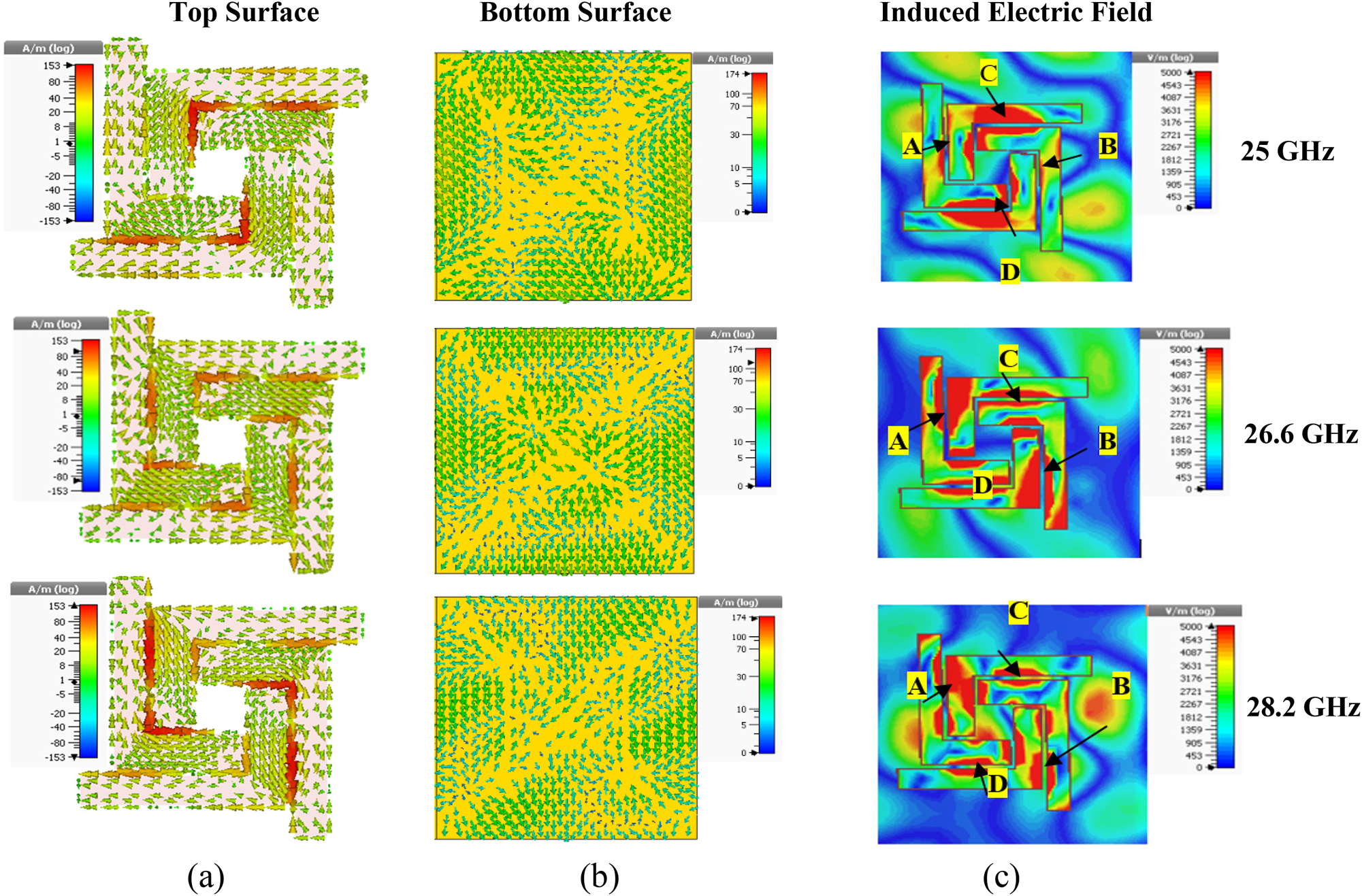
Surface current distribution at different resonance frequencies (a) top (b) bottom, (c) induced electric field of unit cell structure at resonance frequencies.
Electric and magnetic responses are noteworthy at these resonant frequencies. Electric and magnetic responses are noteworthy at these resonant frequencies. Anti-parallel orientation of a surface current at the top metallic patch and the bottom surface of the proposed structure forms the circulating current loop within the structure and hence creating magnetic excitation at these frequencies. The induced electric field distributions at the frequencies of peak absorptivity are shown in Figure 4(c), showing the different part excitement at different resonant frequencies expressing the electric excitation at these frequencies. As depicted in Figure 4(c) large induced electric field can be observed in regions C and D and a comparatively small electric field in regions A and B for 25 GHz. In the same way, at 26.6 GHz and 28.2 GHz field is more concentrated in regions A and B. Simultaneous electric and magnetic excitation of structure at these frequencies produce strong electromagnetic absorption. Further, the factor which significantly affects resonance is the coupling between two adjacent structures, the greater the distance between them weakens the resonance. Constitutive parameters of EM waves like effective permittivity and permeability have been extracted and shown in Figure 5(a) and (b). From Table 1 it is clear that the value of effective permittivity and permeability are showing almost identical values at frequencies of peak absorption, necessary to satisfy the near-zero reflection condition.

Extracted (a) real, and (b) imaginary part of the effective permittivity and permeability.
Extracted permittivity and permeability of broadband polarization-sensitive metamaterial structure.
| Resonance frequency in (GHZ) | Real | Imaginary | ||
|---|---|---|---|---|
| ε eff | μ eff | ε eff | μ eff | |
| 25 GHZ | 20.76 | 21.78 | 37.53 | 37.21 |
| 26.6 GHZ | 22.75 | 23.77 | 41.35 | 41.95 |
| 28.2 GHZ | 26.83 | 27.52 | 52.68 | 52.78 |
3 Parametric analysis and characteristic mode analysis of the structure
The alterable geometric parametric analysis has been studied to examine the effect of various design parameters of the proposed structure on the nature of absorptivity. As depicted in Figure 1(a), L-shaped resonating metallic patches are comprised of two sections. The first section has length a1 and width b1, while the second has length a2 and width b2. The length and width of the section of L shape metallic structures are kept different from maintain maximum absorptivity and bandwidth. When length a1 decreases or increase the peak absorptivity and overall bandwidth shift to the higher and lower frequency side respectively as depicted in Figure 6(a). Similarly, when length a2 decreases and increases the gap g2 increases and decreases respectively. In this case, the overall inductance and capacitive coupling get affected. Hence peak absorptivity and the entire bandwidth shifted to a higher and lower frequency side respectively depicted in Figure 6(b). It is noteworthy from Figure 6(c) and (d) that increment in widths b1 and b2 led to a decrease in gap g1 and g2 led to strong capacitive coupling between each L shape structure. It increases the peak absorptivity while the entire bandwidth shifts towards the lower frequency side.

Effect on absorptivity for the variation of (a) length a1 (b) length a2 (c) length b1 (d) length b2 (e) dimension p (f) permittivity of the substrate.
In the same way, decrement in widths b1 and b2 led to an increase in gap g1 and g2, thus weak capacitive coupling led to peak absorptivity unaltered while the entire bandwidth shrinks slightly. Further placing of unit cells concerning each other keeping other geometrical parameters constant is studied as illustrated in Figure 6(e). With the enhancement in the size of unit cell p, coupling between adjacent top metallic patch decreases hence the overall fringing capacitances reduce, and the absorption frequency shift towards the higher frequency side as evident in Figure 6(e). Reduction in p increases the coupling between the adjacent top metallic patch results an increase in fringing capacitance and shifting of absorption frequency toward the lower side has been observed. The effect of variation on the permittivity of the substrate has also been investigated and it can be observed in Figure 6(f) that the proposed value of εr = 4.3 is showing the optimum absorption performance.
The term radar cross section (RCS) used to measure the detection ability of any object with the signal of RADAR is required to reduce for combat aircraft, tanks, missiles, etc. i.e., reduction in reflected energy towards the RADAR. At the resonance frequency, the radiated energy is concentrated at the surface of the proposed absorber structure. In order to verify the performance of the proposed absorber, the RCS of a proposed prototype is calculated. The RCS of any target is mathematically expressed by [19].
where: σ = radar cross section, Rmax = the maximum radar detection range, Pt = the transmitting power from the radar antenna, Pr = the received power detected by the antenna, G = Gt = Gr is the radar’s transmitting and receiving antennas gain. Equation (8) shows that RCS can be reduced if Pr that is the received power at the radar is reduced either by absorption or scattering. In order to detect any object, the radar must receive a sufficient magnitude of reflected EM wave. More than 90 % absorptivity of EM wave represents very less magnitude (only 10 %) of EM wave is reflecting towards the radar. As pointed out in equation (8) RCS depends on the received EM energy to the radar hence if the EM signal is absorbed in the structure itself then RCS will reduce significantly which is the primary requirement of stealth technology. From this equation, it is evident that RCS depends on received power at the source hence absorption and dissipation of the incoming EM signal in the structure itself reduces the RCS significantly. In the proposed absorber RCS reduction of 35.9 dBm2, 32.4 dBm2, and 34.6 dBm2 is observed at frequencies 25, 26.6, and 28.2 GHz respectively. At resonance frequency, the radiated energy is concentrated at the surface of the proposed absorber structure. Which is the evidence of complete absorption of EM waves.
Further, the CMA analysis of the unit cell has been presented to verify the resonance characteristic of the proposed absorber. Among the several parameters describing the CMA, the characteristic angle βn can be written as [32]:
For a given mode to be resonant its characteristic angle should be 180°, which is equivalent to its eigenmode λn being zero. As illustrated in Figure 7(a) and (b), both βn and λn are 180° and zero, respectively, which confirm the modes at resonance frequencies.

CMA of the designed absorber. (a) Characteristic angle. (b) Eigenvalue. (c) Modal significance.
Another parameter concerning the CMA that can be derived from the eigenmode analysis is the modal significance (MS) which should be one at the resonance. As shown in equation (9) the MS can be defined by [33]:
where λn is the eigenvalue of the mode current (
4 Simulated results of TE and TM polarized wave under normal and oblique incidences
The proposed structure is investigated for different polarization at normal incidence indicated in Figure 8(a) and (b). The direction of incident TE and TM, EM wave is kept constant normal to the structure while the direction of the electric and magnetic field is varied by an angle ɸ in x and y directions. It is observed from the figure that the peak absorptivity and bandwidth remain almost constant for the value of ɸ from 0° to 60° for both TE and TM polarized waves. The four-fold symmetric geometry of the proposed structure makes the absorber insensitive to the direction of the electric and magnetic field in a broader range of frequency at normal incidence. The reflection coefficient for oblique incidence for parallel and perpendicular polarization is given by equations (10) and (11) respectively.
where η1 and η2 are the intrinsic impedances of the mediums respectively. θi and θt are the angle of incidence and transmission. It is clear from the equation that for a larger will. Where η1 and η2 are the intrinsic impedances of the mediums respectively. θi and θt are the angle of incidence and transmission. It is clear from the equation that for a larger value of the angle of oblique incidence, the reflection coefficient increases. Hence the design of the structure is crucial for getting the large reflection coefficient as θi can be large or small. In the case of TE polarization, illustrated in Figure 9(a) the direction of an electric field is kept aligned in the x-direction while the direction of the magnetic field and EM wave is varied at an angle of θ in y and z directions respectively. As evident in Figure 9(a), bandwidth response is almost retained for the wide angle of incidence however whole response shifted to the lower frequency side.

Simulated absorption of proposed structure under different polarization angles (ɸ) for (a) TE polarized wave (b) TM polarized wave.

Simulated absorption of proposed structure under different incidence angles (θ) for (a) TE polarized wave (b) TM polarized wave.
Positions of peaks of absorptivity are not holding at the same positions and the proposed structure is showing more than 80 % absorption of EM wave up to θ = 0–45°. However, the overall bandwidth is narrower than other values of oblique incidence. In the case of TM polarization, illustrated in Figure 9(b) the direction of the magnetic field is kept aligned in the y-direction while the direction of the electric field and EM wave is varied at an angle of θ in x and z directions respectively. Broadband response with nearly more than 80 % absorption has been retained up to θ = 45°. The response has been decreased at θ = 60° for both TE and TM polarizations.
5 Measurement setup and experimental results
In order to validate the concept of broadband absorption at the K-band the proposed absorber structure is fabricated with 16 × 9-unit cells, with an overall dimension of 224 mm × 126 mm × 1.67 mm using printed circuit board (PCB) technology as depicted in Figure 10(a). The schematic of the test setup to measure the absorptivity of the fabricated metamaterial absorber is illustrated in Figure 10(b). For the measurement of absorptivity, first, a copper plate with an identical dimension to that of the fabricated structure, acting as an ideal reflector, is placed in front of the antennas inside the room containing the anechoic chamber and the reflected signal from its top surface has been measured. The two broadband horn antennas (one transmitting antenna and another receiving antenna) are connected to a vector network analyzer Anritsu S820E, where the power spectra have been measured. The complete experimental arrangement for normal incidence is shown in Figure 11(a) and (b).

Fabrication and measurement (a) 16*9 array of unit cell (b) Schematic of test setup to measure the absorptivity of the fabricated metamaterial absorber.

Measurement setup for the proposed metamaterial absorber as (a) horn antennas and array absorber, and (b) VNA setup.
The measured result of absorptivity under the normal incidence of EM wave is showing more than 90 % absorptivity with a slight shift in frequency at the higher side shown in Figure 12(a). The measured response provides a bandwidth of 6.8 GHz between 22.5 and 29.3 GHz maintaining more than 90 % absorptivities over the complete band. The measured absorption peaks are observed at 24.7, 25.5, and 28.4 GHz with peak absorptivities of 95.3, 99.4, and 94.5 % respectively in the absorption bandwidth. The measured result for different polarization angles for TE polarized wave under normal incidence is showing more than 90 % absorptivity depicted in Figure 12(b).

Comparison of simulated and measured results of absorptivity of the proposed absorber. (a) Under normal incidence. (b) Under different polarization angles (ɸ) for TE polarized wave. (c) Under different incidence angles (θ) for TE polarized wave.
Subsequently, the measured result for different oblique incidence angles for TE polarized wave are matching reasonably with slight variations compared to the simulated result confirming the concept of broad-band absorption in the K-band region as illustrated in Figure 12(c). However slight variation in measured results is observed as compared to simulated ones attributed to fabrication tolerances and measurement process.
The performance characteristics of the proposed absorber have been compared with some earlier reported relevant metamaterial absorbers in Table 2. The proposed design shows a combination of all desired characteristics, such as large fractional bandwidth, polarization insensitivity, compact topology, and wide angular stability, while other reported works contain either one or two characteristics. In addition, the geometry offers such a large absorption bandwidth, with the use of a single layer thin substrate (λ0/8), not observed in the existing literature.
Comparison with earlier reported broadband metamaterial absorber.
| Ref. | Thickness (centre freq.) | Resonant frequency band (GHz) | Fractional bandwidth (%) | Polarization insensitive | Incidence angle insensitivity (degree) | |
|---|---|---|---|---|---|---|
| TE | TM | |||||
| [34] | λ0/3 | 12–27 | 77 | No | θ < 45° (above 80 %) | θ < 45° (above 80 %) |
| [35] | λ0/4 | 14.2–32.9 | 79 | No | θ < 60° (above 80 %) | θ < 60° (above 80 %) |
| [36] | λ0/3 | 19.7–20.1 | 4 | Yes | θ < 30° (above 80 %) | θ < 30° (above 80 %) |
| [37] | λ0/6 | 20–30 | 40 | No | θ < 20° (above 80 %) | θ < 30° (above 80 %) |
| Proposed | λ0/8 | 22.56–29.29 | 25.8 | Yes | θ < 45° (above 80 %) | θ < 45° (above 80 %) |
6 Conclusions
In this paper, a broadband wide-angle polarization-insensitive metamaterial absorber has been designed and analyzed. The structure provides an absorption bandwidth of 6.8 GHz starting from 22.5 to 29.3 GHz with more than 90 % absorptivity. The peaks of absorption are observed at frequencies 25, 26.6, and 28.2 GHz having peak absorptivity of 98.7 %, 99 %, and 97.8 % respectively. The resonances are verified with characteristics mode analysis. The absorption mechanism is elaborated with the surface current distribution, induced electric field, and parametric analysis of the geometrical parameters of the proposed structure. The structure is studied for polarization insensitivity under the normal incidence angle which illustrates nearly the same performance for all polarization angles. Fair absorption is observed for the wide angle of θ up to 45° for both TE and TM (more than 80 %) waves at oblique incidence. An equivalent circuit model has been analyzed to validate the proposed design as per circuit theory. The prototype of the proposed structure has been fabricated and absorptivity has been observed experimentally, which illustrates good matching with the simulated results. Broadband response with good polarization insensitivity at normal and oblique incidence makes the, proposed thin (λ0/8) structure commercially suitable for sensing and RCS reduction, at the K-band.
-
Research ethics: Not applicable.
-
Author contributions: All authors have accepted responsibility for the entire content of this manuscript and approved its submission.
-
Competing interests: Authors do not have any conflict of interest.
-
Research funding: None declared.
-
Data availability: The authors confirm that the data supporting the findings of this study are available within the article and there are no supplementary materials. Raw data that support the findings of this study are available with the first and corresponding author, upon reasonable request.
References
[1] N. I. Landy, S. Sajuyigbe, J. J. Mock, D. R. Smith, and W. J. Padilla, “Perfect metamaterial absorber,” Phys. Rev. Lett., vol. 100, no. 20, p. 207402, 2008, https://doi.org/10.1103/physrevlett.100.207402.Search in Google Scholar PubMed
[2] F. Tofigh, M. Amiri, N. Shariati, J. Lipman, and M. Abolhasan, “Polarization-insensitive metamaterial absorber for crowd estimation based on electromagnetic energy measurements,” IEEE Trans. Antennas Propag., vol. 68, no. 3, pp. 1458–1467, 2019, https://doi.org/10.1109/tap.2019.2955275.Search in Google Scholar
[3] L. Dewangan and N. K. Mishra, “Multiband polarization insensitive metamaterial absorber for radar cross-section reduction,” AEU - Int. J. Electron. Commun., vol. 168, p. 154706, 2023, https://doi.org/10.1016/j.aeue.2023.154706.Search in Google Scholar
[4] N. K. Mishra and L. Dewangan, “Broad band polarization insensitive metamaterial absorber for K band application,” in 2022 IEEE Microwaves, Antennas, and Propagation Conference (MAPCON), 2022, pp. 97–100.10.1109/MAPCON56011.2022.10047816Search in Google Scholar
[5] M. Yoo, H. K. Kim, S. Lim, et al.., “Angular- and polarization-insensitive metamaterial absorber using subwavelength unit cell in multilayer technology,” IEEE Antenn. Wireless Propag. Lett., vol. 15, pp. 414–417, 2015, https://doi.org/10.1109/lawp.2015.2448720.Search in Google Scholar
[6] K. Manpreet and S. Hari Shankar, “Analysis of quad-band polarization- and incident-angle independent low profile metamaterial absorber,” Frequenz, vol. 77, nos. 5–6, pp. 235–247, 2023, https://doi.org/10.1515/freq-2022-0059.Search in Google Scholar
[7] J. B. de Araújo, G. L. Siqueira, E. Kemptner, M. Weber, C. Junqueira, and M. M. Mosso, “An ultrathin and ultrawideband metamaterial absorber and an equivalent-circuit parameter retrieval method,” IEEE Trans. Antennas Propag., vol. 68, no. 5, pp. 3739–3746, 2020, https://doi.org/10.1109/tap.2020.2963900.Search in Google Scholar
[8] Z. C. Lin, Y. Zhang, L. Li, Y. T. Zhao, J. Chen, and K. D. Xu, “Extremely wideband metamaterial absorber using spatial lossy transmission lines and resistively loaded high impedance surface,” IEEE Trans. Microwave Theory Tech., vol. 71, no. 8, pp. 3323–3332, 2023. https://doi.org/10.1109/TMTT.2023.3259530.Search in Google Scholar
[9] L. L. Wang, S. B. Liu, H. F. Zhang, X. K. Kong, and L. L. Liu, “High-impedance surface-based flexible broadband absorber,” J. Electromagn. Waves Appl., vol. 31, no. 13, pp. 1216–1231, 2017, https://doi.org/10.1080/09205071.2017.1326850.Search in Google Scholar
[10] T. Wang, M. D. Ding, H. H. He, J. B. Mao, and J. F. Ruan, “Ultra-wideband polarization- and angle-insensitive metamaterial absorber based on multilayer resistive ink,” J. Electromagn. Waves Appl., vol. 36, no. 2, pp. 272–284, 2022, https://doi.org/10.1080/09205071.2021.1965038.Search in Google Scholar
[11] P. Chen, X. Kong, J. Han, et al.., “Wide-angle ultra-broadband metamaterial absorber with polarization-insensitive characteristics,” Chin. Phys. Lett., vol. 38, no. 2, p. 027801, 2021, https://doi.org/10.1088/0256-307x/38/2/027801.Search in Google Scholar
[12] W. Li, M. Xu, H. X. Xu, X. Wang, and W. Huang, “Metamaterial absorbers: from tunable surface to structural transformation,” Adv. Mater., vol. 34, no. 38, p. 2202509, 2022, https://doi.org/10.1002/adma.202202509.Search in Google Scholar PubMed
[13] J. Fang, J. Huang, Y. Gou, and Y. Shang, “Research on broadband tunable metamaterial absorber based on PIN diode,” Optik, vol. 200, p. 163171, 2020, https://doi.org/10.1016/j.ijleo.2019.163171.Search in Google Scholar
[14] D. Hassan, T. Hamed, R. S. Hassan, T. G. Jahani, and M. Ali, “Thermally switchable terahertz metasurface absorber composed of H-fractal and enabled by phase-change material of vanadium dioxide,” Frequenz, vol. 76, nos. 3–4, pp. 169–175, 2022, https://doi.org/10.1515/freq-2021-0147.Search in Google Scholar
[15] S. Bhattacharyya, S. Ghosh, D. Chaurasiya, and K. V. Srivastava, “Bandwidth-enhanced dual-band dual-layer polarization-independent ultra-thin metamaterial absorber,” Appl. Phys. A, vol. 118, pp. 207–215, 2015, https://doi.org/10.1007/s00339-014-8908-z.Search in Google Scholar
[16] S. Ghosh, S. Bhattacharyya, D. Chaurasiya, and K. Srivastava, “Polarisation-insensitive and wide-angle multi-layer metamaterial absorber with variable bandwidths,” Electron. Lett., vol. 51, no. 14, pp. 1050–1052, 2015, https://doi.org/10.1049/el.2015.1167.Search in Google Scholar
[17] Y. Shi, Y. C. Li, T. Hao, L. Li, and C. H. Liang, “A design of ultra-broadband metamaterial absorber,” Waves Random Complex Media, vol. 27, no. 2, pp. 381–391, 2017, https://doi.org/10.1080/17455030.2016.1250974.Search in Google Scholar
[18] S. Ghosh, S. Bhattacharyya, and K. V. Srivastava, “Design, characterisation and fabrication of a broadband polarisation-insensitive multi-layer circuit analogue absorber,” IET Microw., Antennas Propag., vol. 10, no. 8, pp. 850–855, 2016, https://doi.org/10.1049/iet-map.2015.0653.Search in Google Scholar
[19] L. Dewangan, M. S. Patinavalasa, J. Acharjee, Y. Solunke, S. Ghosh, and N. K. Mishra, “Broadband metamaterial absorber for stealth applications at K-band,” AEU-International Journal of Electronics and Communications, vol. 170, p. 154828, 2023, https://doi.org/10.1016/j.aeue.2023.154828.Search in Google Scholar
[20] H. Wang, V. P. Sivan, A. Mitchell, G. Rosengarten, P. Phelan, and L. Wang, “Highly efficient selective metamaterial absorber for high-temperature solar thermal energy harvesting,” Sol. Energy Mater. Sol. Cells, vol. 137, pp. 235–242, 2015, https://doi.org/10.1016/j.solmat.2015.02.019.Search in Google Scholar
[21] Z. Xiao, F. Lv, W. Li, and H. Zou, “A three-dimensional ultra-broadband and polarization insensitive metamaterial absorber and application for electromagnetic energy harvesting,” Waves Random Complex Media, vol. 31, no. 6, pp. 2168–2176, 2021, https://doi.org/10.1080/17455030.2020.1733705.Search in Google Scholar
[22] A. E. Culhaoglu, A. V. Osipov, and P. Russer, “Mono- and bistatic scattering reduction by a metamaterial low reflection coating,” IEEE Trans. Antennas Propag., vol. 61, no. 1, pp. 462–466, 2012, https://doi.org/10.1109/tap.2012.2220095.Search in Google Scholar
[23] J. Xie, S. Quader, F. Xiao, et al.., “Truly all-dielectric ultra broadband metamaterial absorber: water-based and ground-free,” IEEE Antenn. Wireless Propag. Lett., vol. 18, no. 3, pp. 536–540, 2019, https://doi.org/10.1109/lawp.2019.2896166.Search in Google Scholar
[24] F. O. Alkurt, O. Altintas, A. Atci, et al.., “Antenna-based microwave absorber for imaging in the frequencies of 1.8, 2.45, and 5.8 GHz,” Opt. Eng., vol. 57, no. 11, p. 113102, 2018, https://doi.org/10.1117/1.oe.57.11.113102.Search in Google Scholar
[25] J. Grant, M. Kenney, Y. D. Shah, I. Escorcia-Carranza, and D. R. S. Cumming, “CMOS compatible metamaterial absorbers for hyperspectral medium wave infrared imaging and sensing applications,” Opt. Express, vol. 26, no. 8, pp. 10408–10420, 2018, https://doi.org/10.1364/oe.26.010408.Search in Google Scholar
[26] B. X. Wang, X. Zhai, G. Z. Wang, W. Q. Huang, and L. L. Wang, “A novel dual-band terahertz metamaterial absorber for a sensor application,” J. Appl. Phys., vol. 117, no. 1, p. 014504, 2015, https://doi.org/10.1063/1.4905261.Search in Google Scholar
[27] H. Singh, A. Gupta, R. S. Kaler, S. Singh, and A. S. Gill, “Designing and analysis of ultrathin metamaterial absorber for W band biomedical sensing application,” IEEE Sens. J., vol. 22, no. 11, pp. 10524–10531, 2022, https://doi.org/10.1109/jsen.2022.3168827.Search in Google Scholar
[28] H. Xu, L. Hu, Y. Lu, J. Xu, and Y. Chen, “Dual-band metamaterial absorbers in the visible and near-infrared regions,” J. Phys. Chem. C, vol. 123, no. 15, pp. 10028–10033, 2019, https://doi.org/10.1021/acs.jpcc.9b00434.Search in Google Scholar
[29] H. Huang, H. Xia, W. Xie, Z. Guo, H. Li, and D. Xie, “Design of broadband graphene-metamaterial absorbers for permittivity sensing at mid-infrared regions,” Sci. Rep., vol. 8, no. 1, p. 4183, 2018, https://doi.org/10.1038/s41598-018-22536-x.Search in Google Scholar PubMed PubMed Central
[30] Y. Jang, M. Yoo, and S. Lim, “Conformal metamaterial absorber for curved surface,” Opt. Express, vol. 21, no. 20, pp. 24163–24170, 2013, https://doi.org/10.1364/oe.21.024163.Search in Google Scholar
[31] S. Kalraiya, R. K. Chaudhary, and M. A. Abdalla, “Design and analysis of polarization independent conformal wideband metamaterial absorber using resistor loaded sector shaped resonators,” J. Appl. Phys., vol. 125, no. 13, p. 134904, 2019, https://doi.org/10.1063/1.5085253.Search in Google Scholar
[32] Y. Wu, H. Lin, J. Xiong, et al.., “A broadband metamaterial absorber design using characteristic modes analysis,” J. Appl. Phys., vol. 129, no. 13, p. 134902, 2021, https://doi.org/10.1063/5.0043054.Search in Google Scholar
[33] P. Ylä-Oijala, H. Wallén, and S. Järvenpää, “Theory of characteristic modes for lossy structures: formulation and interpretation of eigenvalues,” Int. J. Numer. Model.: Electron. Netw. Devices Fields, vol. 33, no. 2, p. e2627, 2020, https://doi.org/10.1002/jnm.2627.Search in Google Scholar
[34] C. Barde, A. Choubey, and R. Sinha, “Wide band metamaterial absorber for Ku and K band applications,” J. Appl. Phys., vol. 126, no. 17, p. 175104, 2019, https://doi.org/10.1063/1.5119311.Search in Google Scholar
[35] S. Shi, X. Qiao, and Q. Jia, “A compact ultra-broadband metamaterial absorber for Ku-, K-, and Ka-band applications,” Phys. Scr., vol. 96, no. 12, p. 125522, 2021, https://doi.org/10.1088/1402-4896/ac2efa.Search in Google Scholar
[36] M. L. Hakim, T. Alam, M. T. Islam, M. H. Baharuddin, and A. Alzamil, “Quad-band polarization-insensitive square split-ring resonator (SSRR) with an inner Jerusalem cross metamaterial absorber for Ku- and K-band sensing applications,” Sensors, vol. 22, no. 12, p. 4489, 2022, https://doi.org/10.3390/s22124489.Search in Google Scholar PubMed PubMed Central
[37] R. M. Bilal, M. A. Baqir, P. K. Choudhury, et al.., “Wideband microwave absorber comprising metallic split-ring resonators surrounded with E-shaped fractal metamaterial,” IEEE Access, vol. 9, pp. 5670–5677, 2021, https://doi.org/10.1109/access.2020.3048927.Search in Google Scholar
© 2023 Walter de Gruyter GmbH, Berlin/Boston
Articles in the same Issue
- Frontmatter
- Research Articles
- Deep learning based distorted Born iterative method for improving microwave imaging
- Direction independent broad-band wide angle metamaterial absorber for “K” band applications
- Wide angle metamaterial absorber for S, C and X band application
- Design of the Wilkinson power divider with multi harmonic suppression
- Equivalent circuit of a planar microwave liquid sensor based on metamaterial complementary split ring resonator
- A novel slotted dumbbell-shaped dielectric resonator antenna with enhanced bandwidth for C-band and 5G sub-6 GHz applications
- Profile reduction of folded transmitarray antenna using multiple feeders
- Short Communication
- Graphene based waveguide fed hybrid plasmonic terahertz patch antenna