III–V Multijunction Solar Cell Integration with Silicon: Present Status, Challenges and Future Outlook
-
Nikhil Jain


Abstract
Achieving high-efficiency solar cells and at the same time driving down the cell cost has been among the key objectives for photovoltaic researchers to attain a lower levelized cost of energy (LCOE). While the performance of silicon (Si) based solar cells have almost saturated at an efficiency of ~25%, III–V compound semiconductor based solar cells have steadily shown performance improvement at ~1% (absolute) increase per year, with a recent record efficiency of 44.7%. Integration of such high-efficiency III–V multijunction solar cells on significantly cheaper and large area Si substrate has recently attracted immense interest to address the future LCOE roadmaps by unifying the high-efficiency merits of III–V materials with low-cost and abundance of Si. This review article will discuss the current progress in the development of III–V multijunction solar cell integration onto Si substrate. The current state-of-the-art for III–V-on-Si solar cells along with their theoretical performance projections is presented. Next, the key design criteria and the technical challenges associated with the integration of III–V multijunction solar cells on Si are reviewed. Different technological routes for integrating III–V solar cells on Si substrate through heteroepitaxial integration and via mechanical stacking approach are presented. The key merits and technical challenges for all of the till-date available technologies are summarized. Finally, the prospects, opportunities and future outlook toward further advancing the performance of III–V-on-Si multijunction solar cells are discussed. With the plummeting price of Si solar cells accompanied with the tremendous headroom available for improving the III–V solar cell efficiencies, the future prospects for successful integration of III–V solar cell technology onto Si substrate look very promising to unlock an era of next generation of high-efficiency and low-cost photovoltaics.
Introduction and motivation
III–V compound semiconductor based multijunction solar cells have been the most successful technology for delivering the highest photovoltaic conversion efficiency for space power applications. In spite of achieving the highest conversion efficiency among all the competing photovoltaic technologies, their expensive cost has been the biggest impediment in their large-scale deployment for terrestrial applications. The performance of single-junction (1J) Si solar cells has almost saturated at ~25%, with the most recent accomplishment of 25.6% efficiency taking more than 15 years for an absolute 0.6% improvement in efficiency (Green et al. 2014). Interestingly, III–V solar cells have steadily shown performance improvement at ~1% (absolute) increase in efficiency per year, with the most recent world record efficiency of 44.7% at 297 suns for a four-junction III–V solar cell (Bett et al. 2013). However, the dominance of silicon solar cells and their plummeting prices in the recent years have made it challenging for high-efficiency III–V solar cells to make a strong commercial impact.
One of the most significant cost contributors to the bill of materials for III–V solar cells is the cost of the starting substrate. Typically, GaAs or Ge substrates are used for III–V multijunction solar cell growth, which are not only smaller in diameter but are also significantly more expensive than the Si substrate. Successful integration of III–V solar cells on Si substrate can offer a great promise for lowering the future levelized cost of energy (LCOE) by unifying the high-efficiency merits of the III–V materials with the low-cost and abundance of the Si substrate. In addition to the substantial cost benefits associated with the larger area, and low-cost of Si substrate, Si also offers higher thermal conductivity and superior mechanical strength in comparison to GaAs or Ge substrates. III–V multijunction solar cell integration on Si substrate could potentially use the starting Si substrate as an active bottom subcell or perhaps just as an inactive starting template. With a bandgap of 1.12 eV, Si substrate is a better bottom cell candidate in comparison to Ge substrate (bandgap – 0.67 eV) for integration with standard dual-junction (2J) InGaP/GaAs based multijunction solar cells in regard to current-matching (Derendorf et al. 2013). Such triple-junction (3J) InGaP/GaAs//Si solar cells (monolithically or mechanically stacked) are likely to be the quickest path for high-efficiency III–V-on-Si solar cells (Green 2014) with theoretically efficiency in excess of 40% at AM1.5g and AM1.5d (Derendorf et al. 2013; Yang et al. 2014). A recent study has revealed that transitioning from a 4” Ge substrate to a 8” Si substrate would correlate to about 60% reduction in cost for multijunction solar cells (D’Souza et al. 2011). When utilizing Si as an inactive starting template, III–V-on-Si technology could leverage commercially available substrate re-use techniques such as spalling (Shahrjerdi et al. 2012) and epitaxial lift-off (Tatavarti et al. 2010) to explore additional cost savings schemes. The research on integrating III–V compound semiconductor materials on Si substrate for photovoltaic application was initiated in 1980s. However, the complexity associated with the material growth, reliability and reproducibility led to decline in the research for III–V-on-Si solar cells in the late 1990s. In the last 5–6 years, III–V-on-Si solar cell research has re-gained attention pertaining to the research on new metamorphic buffer approaches, wafer bonding and mechanical stacking techniques. With the declining cost of Si combined with the impressive headroom available for improving the performance of III–V solar cells, future prospects for successful integration of III–V solar cell technology onto Si substrate look very promising.
This review article will first discuss the current state-of-the-art for III–V-on-Si solar cells and the theoretical performance projections for III–V-on-Si solar cell technology. Next, the key design criteria and the technical challenges associated with integrating III–V multijunction solar cells on Si are summarized. Thereafter, in-depth discussion on various technological routes for integrating III–V solar cells on Si substrate through heteroepitaxial integration and through mechanical stacking is presented. Next, the key merits and technical challenges for all of the till-date available technologies are reviewed. Finally, the prospects, opportunities and future outlook toward further advancing the performance of III–V-on-Si multijunction solar cells are presented.
Design criteria and challenges
There are two key approaches for integrating III–V multijunction solar cells on Si substrate: (i) heteroepitaxial growth (or monolithic) and (ii) mechanical stacking (and wafer bonding). The terms mechanical stacking and wafer bonding will be used interchangeably in this article. The following section reviews the key design criteria and technical challenges associated with both of these integration approaches.
Heteroepitaxial approach for III–V-on-Si integration
Heteroepitaxial integration approach is believed to be a very promising path to integrate high-efficiency III–V solar cells onto Si substrate owing to the utilization of single substrate and single epitaxial process. Lattice-matched 2J InGaP/GaAs solar cells have been the key building block for today’s most efficient 3J and quadruple junction (4J) III–V solar cells, with GaAs being predominantly used as the starting substrate. Hence, integration of GaAs-on-Si substrate was the initial and the natural choice for realizing a “GaAs-on-Si” virtual platform for the subsequent multijunction solar cell growth (Vernon et al. 1986; Yamaguchi et al. 1988; Soga et al. 1995). More recently, approaches involving metamorphic graded buffers such as GaAsP and SiGe have gained a lot of attention for III–V/Si tandem solar cells (Grassman, Carlin, and Ringel 2010; Andre et al. 2005; Dimroth et al. 2014; Diaz et al. 2014; Yaung, Lang, and Lee 2014). Additional heteroepitaxial integration approaches, which in comparison to the previously mentioned techniques have been less extensively explored, include – (i) lattice-matched dilute nitride (GaAsPN) solar cells on Si substrate (Geisz et al. 2005; Almosni et al. 2013; Yamane et al. 2014) and (ii) lattice-mismatched InGaN based solar cells (Ager et al. 2008; Brown et al. 2010; Tran et al. 2012) on Si substrate. The most critical challenges associated with heteroepitaxial integration of III–V materials on Si substrate are highlighted as follows:
Growth of lattice-mismatched III–V materials on Si substrate
The 4% lattice-mismatch between GaAs and Si makes the direct epitaxy of GaAs on Si extremely challenging, resulting in the formation of defects and dislocations such as threading dislocations and misfit dislocations. Such defects and dislocations have a detrimental impact on the minority carrier lifetime and hence the solar cell performance. The most noteworthy techniques which have been employed for direct GaAs epitaxy on Si to reduce the threading dislocation density (TDD) include (i) the thermal-cycle annealing (TCA) (Yamaguchi, Nishioka, and Sugo 1989; Yamaguchi 1991) and (ii) the low temperature and low growth rate process during the initial GaAs nucleation on Si (Vernon et al. 1986; Tran et al. 2012; Yamaguchi, Nishioka, and Sugo 1989; Yamaguchi 1991; Bolkhovityanov and Pchelyakov 2008). Growing thicker GaAs buffers has also been shown to facilitate dislocation reduction (Vernon et al. 1986) but adds to the overall cost and time of the epitaxial process. Additionally, thin strained layers (SLs) and superlattices introduced into the bulk GaAs buffer have been shown to facilitate the annihilation of TDs and minimize the dislocation propagation into the active layers of interest. Such an approach led to one of the highest efficiencies for heteroepitaxial 1J GaAs-on-Si solar cells (Ohmachi et al. 1988; Yamaguchi 2014). More recent approaches involve the growth of metamorphic graded buffers (e.g. SiGe, GaAsP) to bridge the lattice constant between the Si and GaAs (or GaAsP) (Grassman, Carlin, and Ringel 2010; Andre et al. 2005; Dimroth et al. 2014; Diaz et al. 2014; Yaung, Lang, and Lee 2014). One of the most successful approaches in regard to dislocation reduction has been the utilization of graded SiGe buffers; however, such buffers are very thick, and their low bandgap precludes the use of the Si substrate as an active bottom cell. The larger bandgap of GaAsP buffers could circumvent the problem of utilizing the Si substrate as an active subcell. Among the various heteroepitaxial approaches employed for III–V-on-Si epitaxy, the SiGe graded buffer (Andre et al. 2005) and the direct GaAs on Si epitaxial approach involving SL superlattices (SLSs) (Yamaguchi, Nishioka, and Sugo 1989) have reported the lowest TDD ~1×106 cm−2. Further dislocation reduction to ~1×105 cm−2 would enable the GaAs-on-Si solar cells to compete with lattice-matched GaAs-on-GaAs solar cells.
Heteroepitaxy of polar III–V materials on non-polar Si substrate
Growth of compound semiconductors (e.g. GaAs) on monoatomic semiconductors (e.g. Si, Ge) results in the formation of antiphase domains (APDs) which are structural defects generated due to heteroepitaxy of polar material (GaAs) on non-polar materials (Ge or Si). The (001) surface of Si substrate consists of monoatomic steps in which Si atoms are arranged in form of dimers oriented in perpendicular directions across two adjacent steps. During the initial stage of GaAs-on-Si growth, the arsenic dimers follow the dimer orientations of the underlying Si layer and orient themselves in perpendicular directions across the adjacent steps leading to the formation of As–As or subsequent Ga–Ga bonds, which initiates the formation of antiphase boundaries. Significant research has been devoted to minimize the formation of APDs. Utilization of offcut Si substrates (4˚–6˚) with double-layer step formation with the adjacent Si–Si dimers in identical orientation facilitates similar trend for the subsequent GaAs, thus minimizing the formation of APDs (Bolkhovityanov and Pchelyakov 2008).
Thermal mismatch between III–V materials and Si substrate
The inherent difference in the thermal expansion coefficient (5.73×10⁻⁶ °C−1 for GaAs and 2.6×10⁻⁶ °C−1 for Si) and the difference in the lattice-mismatch between GaAs and Si lead to residual strain in the films and the formation of defects and dislocations through lattice strain relaxation which could result in poor crystalline quality. The defects and dislocations are primarily categorized into APDs, misfit and threading dislocations, twinning and stacking faults. One of the major concerns regarding the thermal mismatch is the generation of microcracks in the GaAs epitaxial layer which could pose serious problems related to solar cell reliability besides limiting the device area and performance. Faster sample cooling rate promotes microcrack formation, hence it is extremely important to control the cooling rate to minimize the microcrack density. Continued investigations to better understand the correlation between thermal mismatch and solar cell characteristics would be essential to validate the reliability and long-term robustness for GaAs-on-Si solar cells.
Buffer design – thickness, optical transparency, electrical conductivity and surface passivation.
An appropriate buffer selection is extremely critical for the success of III–V-on-Si solar cells. Optically transparent and thin buffer layers are desirable in order to utilize the starting Si substrate as an active cell, while the electrical conductivity of the buffer becomes more important for concentrated photovoltaic (CPV) to minimize series resistance. Most of the metamorphic graded buffer approaches utilize a thick buffer layer to bridge the lattice constant between the III–Vs and Si. The lattice-matched dilute nitride buffers (GaAsPN) on Si and direct GaAs-on-Si buffers with SLS are among the choices which could offer comparatively thinner heteroepitaxial buffers. In terms of optical transparency for active bottom Si substrate cell, wide bandgap GaAsP graded buffer would be a better choice than low-bandgap SiGe buffers. Interestingly, the SiGe buffers could serve as active bottom subcell offering bandgap and lattice constant tunability to allow integration with top GaAsP subcell for tandem cell designs (Diaz et al. 2014). An additional important buffer selection criteria is to utilize a layer which would provide a good surface passivation for the bottom Si subcell and serve as a window layer. Thus, there are important design trade-offs between the respective buffer selections in relation to minimizing the dislocation density while enabling thin and optically transparent buffers for utilizing Si substrate as an active solar cell.
Mechanical stacking approach for III–V-on-Si integration
The approach of mechanical stacking for III–V-on-Si integration can accommodate large amount of lattice-mismatch and enable the integration of materials with ideal bandgap combination which are free from lattice-mismatch constraints unlike in heteroepitaxial growth approach. The most critical challenges associated with the mechanical stacking approach for integrating III–V materials and solar cell structures on Si substrate are highlighted as follows:
Post-growth bonding approaches are favorable, otherwise the bond interface would go through the high temperature epitaxial growth process and could potentially suffer from thermal mismatch between the III–V materials and Si leading to wafer bowing or cracking.
The bonding temperature must be compatible with the III–V materials and the Si substrate.
The bonding layer should be thin and optically transparent to allow the utilization of bottom Si substrate as an active subcell.
For two-terminal solar cell operation under concentrated sunlight, it is of critical importance to realize electrically conductive bond layers to avoid adding series resistance.
The bonding interfaces should have low surface roughness and must be free from native oxides.
Viable III–V substrate removal and re-utilization process with high yield and high throughput.
III–V and Si solar cell design and challenges
Si being an indirect bandgap semiconductor typically limits the overall current when integrated in tandem with conventional 2J InGaP/GaAs solar cells in 3J two-terminal configuration (Derendorf et al. 2013; Yang et al. 2014; Jain et al. 2014; Garcia-Tabares et al. 2011). Hence, the design of bottom Si subcell is extremely important for current-matching in tandem cell design. An additional important role of the initial III–V layer on Si is to serve as effective window layer, allowing sufficient optical transmission, surface passivation, majority carrier conduction and minority carrier reflection. Emitter formation in the Si substrate can be challenging, and different approaches are being explored, such as in-situ epitaxial phosphorus diffusion (Garcia-Tabares et al. 2011), in-situ epitaxial growth of Si emitter (Ringel et al. 2013) and ex-situ conventional diffusion. The in-situ phosphorus diffusion from the gas phase was found to be less intense for optimal junction formation in Si (Ringel et al. 2013), translating to epitaxially grown or ex-situ diffused junctions being more efficient. Although, III–V/Si interface passivation is essential for subsequent III–V epitaxial growth, the influence of front surface recombination is not critical for multijunction designs, since the top III–V subcells would absorb most of the photons in the wavelength range which is affected by the III–V/Si interface, and only the high-wavelength photons would reach the bottom Si subcell, hence a less severe impact on the short-circuit current density (Jsc) of Si solar cell. Thinner Si emitters are preferred to maximize both the open circuit voltage (Voc) and Jsc when the interface recombination velocity (IRV) is low, however there is a strong trade-off between optimizing the Voc and Jsc when the IRV is high (Grassman et al. 2014). For selecting the optimal doping in the emitter, lightly doped Si emitter maximizes the Voc when the IRV is low, while heavily doped emitter designs translate to higher Voc when the IRV is high (Al Mansouri et al. 2013). The most important design criterion for utilizing Si as an active subcell with III–V subcells in a multijunction configuration would be to engineer the backside of the Si substrate to enhance back surface reflection and achieve good surface passivation because Si subcell typically limits the current in III–V/Si tandem cell designs (Derendorf et al. 2013; Jain et al. 2014). Numerical simulations reveal that a silicon nitride passivation layer along with aluminum back reflector would provide substantial boost in quantum efficiency (QE) for higher wavelength regime of the spectrum and enable Jsc >14 mA/cm2 in the bottom Si subcell for successful integration with III–V multijunction solar cells (Martin, Garcia-Tabares, and Rey-Stolle 2013).
In terms of the III–V solar cell designs on Si, most crucial challenges are the reduction of TDDs and realization of high-quality solar cell materials with bandgap-voltage offset (Woc) close to the radiative limit of 0.3–0.4 eV. The TDs act as recombination centers for minority carriers, thus degrading the minority carrier lifetimes. Higher dislocation density more adversely affects the Voc than the Jsc in a solar cell. The major effect of TDs generated due to lattice-mismatch on the Voc and fill-factor (FF) is attributed to the increased n = 2 reverse saturation current associated with bulk space-charge recombination due to the reduced minority carrier lifetime (Vernon et al. 1990; Jain and Hudait 2013). Minimizing the lattice-mismatch induced defects and dislocations is expected to improve the minority carrier diffusion length and hence the overall solar cell performance. Realization of high-quality tunnel junction is also a major challenge for connecting new metamorphic solar cell materials such as SiGe, GaAsP, InGaP, GaAsPN, GaPN and InGaN for realizing tandem III–V/Si solar cells. An additional extremely important design aspect is the realization of the current-matching condition taking into account the impact of TDs in metamorphic multijunction solar cells. Careful consideration of all these design challenges would be very critical for the success of III–V multijunction solar cells on Si.
State-of-the-art results and efficiency projections for III–V-on-Si solar cells
With the recent advancements in both heteroepitaxial and mechanical stacking integration approaches for III–V-on-Si solar cells, 3J GaInP/GaAs//Si solar cells have now achieved two-terminal efficiencies in excess of 27% (AM1.5d spectrum) under concentrated sunlight (Bett et al. 2013), with substantial headroom for further improvement. The best experimental results for III–V-on-Si solar cells are summarized in Table 1 along with the respective data for the solar cell figure-of-merits (efficiency (ɳ), sun concentration, Voc, Jsc and FF. Only two-terminal efficiencies are included in Table 1. A four-terminal GaAs–Si dual-junction solar cell with an efficiency of 31% under 347-sun AM1.5d was demonstrated in 1988 (Gee and Virshup 1988). More recently, a spectral beam-splitting system utilizing independent 2J GaInP/GaAs, a Si and a GaSb solar cell achieved an efficiency of 34.3% under 1-sun AM1.5d (Mitchell et al. 2001).
III–V on Si solar cells – state-of-the-art experimental results
| Group/institution | η [%] | Suns | Voc [V] | Jsc [mA/cm2] | FF [%] | Spectrum | Remarks | |
| 3J | Fraunhofer ISE (Bett et al. 2013; Derendorf et al. 2013) | 27.9 | 48 | 3.33 | 614 | 82.9 | AM1.5d | Wafer-bonding (CPV) |
| 20.5 | 1 | 2.78 | 8.56 | 86.3 | AM1.5d | Wafer-bonding | ||
| McMaster University (Yang et al. 2014) | 25.5 | 1 | 2.74 | 11.80 | 79.0 | AM1.5g | Direct metal interconnect | |
| 2J | Fraunhofer ISE (Dimroth et al. 2014) | 26.0 | 1 | 2.385 | 12.70 | 85.9 | AM1.5g | Wafer-bonding |
| University of Tokyo (Tanabe, Watanabe, and Arakawa 2012) | 25.2 | 1 | 1.55 | 27.9 | 58.0 | Wafer-bonding | ||
| Nagoya Institute (Soga et al. 1997) | 21.2 | 1 | 1.57 | 23.6 | 77.2 | AM0 | GaAs/AlGaAs buffer | |
| Multiple (Diaz et al. 2014) | 18.9 | 1 | 1.45 | 18.1 | 72.0 | AM1.5g | SiGe buffer | |
| Ohio State University (Lueck et al. 2006) | 16.8 | 1 | 2.18 | 10.48 | 73.3 | AM1.5g | SiGe buffer | |
| Fraunhofer ISE (Dimroth et al. 2014) | 16.4 | 1 | 1.94 | 11.20 | 75.3 | AM1.5g | GaAsP buffer | |
| 1J | Spire/NREL (Vernon et al. 1991) | 21.3 | 200 | – | – | – | AM1.5d | GaAs buffer (CPV) |
| NTT Japan (Ohmachi et al. 1988) | 20.0 | 1 | AM1.5g | Strained-layer superlattice & GaAs/AlGaAs buffer | ||||
| 18.3 | 1 | 0.94 | 33.2 mA | 79.1 | AM0 | |||
| Ohio State University (Andre et al. 2005) | 18.1 | 1 | 0.973 | 23.8 | 78.1 | AM1.5g | 10 µm SiGe buffer | |
| Spire/NREL (Vernon et al. 1988) | 17.6 | 1 | 0.891 | 25.5 | 77.7 | AM1.5 | 7 µm GaAs buffer |
The state-of-the-art results for III-V-on-Si solar cells are shown in Fig. 1 along with the projected iso-efficiencies for series-connected 2J and 3J solar cells under respective incident solar spectrums. The projected efficiencies for 2J (yellow-dashes) and 3J (green-dashes) cells assume bandgaps of 1.7/1.1 eV and 1.8/1.4/1.1 eV, respectively (Geisz and Friedman 2002). Iso-efficiencies in Fig. 1 were calculated assuming that the thickness of the top junction was optimized for each bandgap combination (Kurtz et al. 1990). The efficiency numbers in red represent results for III–V-on-Si mechanically stacked solar cells, while the numbers in blue represent the results for III–V-on-Si solar cells realized using heteroepitaxial integration. Although iso-efficiency results predict efficiencies in excess of 40% for 3J III–V on Si tandem solar cells (Derendorf et al. 2013), such analysis typically does not take into account the indirect bandgap of Si, the dislocation-dependent current-matching, dislocation-dependent minority carrier lifetimes, surface recombination velocities and the tunnel-junction design. Several groups have been investigating III–V-on-Si solar cell designs which provide more realistic performance projections taking into account the impact of dislocations and surface recombination velocities. Using finite element analysis, Jain et al. showed that a 2J InGaP/GaAs solar cell on Si could achieve efficiency in excess of 29% (AM1.5g – 1,000 W/m2, 1 sun) (Jain and Hudait 2013) and 33% (AM1.5d – 900 W/m2, 600 suns) (Jain and Hudait 2014) at a realistic TDD of 106 cm−2. Using a similar finite element analysis modeling approach, Brown et al. showed that a 2J InGaN/Si tandem cell could achieve an efficiency of 28.9% under AM1.5 illumination (Brown et al. 2010). Triple-junction InGaP/GaAs//Si solar cells have also been numerically investigated as a function of TDD under 1 sun (Yang et al. 2014; Wilkins et al. 2013; Jain et al. 2014) and concentrated sunlight (Jain et al. 2014). Efficiencies exceeding 33% seems feasible at a realistic TDD of 106 cm−2 under 200-sun AM1.5d (1,000 W/m2) spectrum (Jain et al. 2014). Using areal current-matching (ACM), a 2J GaInP/GaAs connected onto an enlarged bottom Si subcell is predicted to have 3J efficiencies exceeding 43% under 1-sun AM1.5g spectrum (Yang et al. 2014). Novel solar cell designs may be feasible by employing Si as an intermediate subcell instead of the bottommost subcell; however, it is extremely challenging to experimentally realize such cell structures. Connolly et al. have modeled 3J GaAs/Si/In0.74Ga0.26As and 3J GaAs0.77P0.23/Si/In0.74Ga0.26As solar cells with efficiencies of 32.9% and 36.5%, respectively, under 1-sun AM1.5g spectrum (Connolly et al. 2013). 4J AlGaAs/GaAs/Si/InGaAs tandem solar cells utilizing Si as an intermediate subcell could achieve efficiencies exceeding of 45% (Mathews et al. 2012). Although achieving such milestones will be experimentally very challenging, these modeling results showcase a promising potential for III–V-on-Si solar cells.
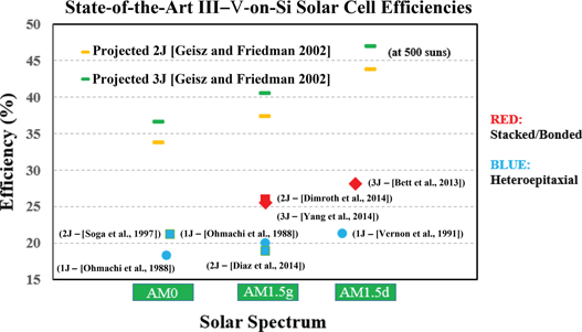
Present state-of-the-art III–V-on-Si experimental solar cell results for AM0, AM1.5g and AM1.5d spectrums. The projected iso-efficiencies for 2J and 3J solar cells under the respective spectrums are shown in yellow and green, respectively. Results for both heteroepitaxial and mechanically stacked integration approaches are shown in blue and red, respectively
Integration approaches for III–V-on-Si solar cells
Heteroepitaxial integration of III–V materials on Si substrate
Direct GaAs-on-Si epitaxy
Among various approaches being investigated for III–V-on-Si integration for solar cell applications, the direct GaAs-on-Si epitaxial approach was among the very first ones. For realizing high-quality GaAs epitaxial layers on Si substrate, the use of TCA has been proven to be a very important step for dislocation reduction. The transmission electron microscopy (TEM) micrographs for GaAs directly grown on Si along with their respective TDDs using TCA only and TCA along with InGaAs SL are shown in Figure 2(a) and (b), respectively (Takano et al. 1998; Soga et al. 1996). The insertion of an SL during the GaAs on Si growth relieves the need for high-temperature TCA and multiple TCA iterations.

Cross-sectional TEM image of heteroepitaxial GaAs grown on Si using (a) only TCA (and Soga et al. 1996), (b) TCA along with In0.07Ga0.93As SL (Takano et al. 1998), reprinted with permission from Takano et al. (1998) and Soga et al. (1996). References Takano et al. (1998) Copyright 1998, AIP Publishing LLC; Soga et al. (1996) Copyright 1996, AIP Publishing LLC
Spire Corporation utilized direct GaAs-on-Si epitaxy involving thick GaAs buffer layer to realize 1J GaAs solar cell on Si substrate for 1-sun and CPV application using thermal-cycle growth (TCG) by metal organic chemical vapor deposition (MOCVD) technique (Vernon et al. 1986, 1988, 1990, 1991). A low temperature GaAs nucleation layer was grown at 400˚C followed by the standard GaAs growth at 700˚C. Ellipsometry studies showed that the presence of arsine during the Si bakeout was one of the major sources of oxide formation (Vernon et al. 1986). For a 1J GaAs cell structure, a 7-µm thick n+ GaAs buffer was employed between the cell structure and the Si substrate. An efficiency of 17.6% (Jsc = 25.5 mA/cm2, Voc = 0.891 V and FF = 77.7%) was reported for 1J GaAs solar cell on Si under AM1.5 at a TDD of ~8×106 cm−2 (Vernon et al. 1988). Utilizing a similar growth process with 2-µm GaAs buffer, 1J GaAs concentrator solar cell on Si with an efficiency of 21.3% under 200 suns (AM1.5d) were also reported (Vernon et al. 1991).
Soga et al. (1996) utilized AlGaAs as an active solar cell material for integration with active Si substrate. Al0.22Ga0.78As with a bandgap of ~1.7 eV is one of the ideal candidates for 2J III–V/Si tandem solar cell. However, the growth of AlGaAs active solar cell material on Si becomes more complex and challenging with increased aluminum (Al) content as it incorporates more oxygen and forms deep level defects which can act as recombination centers for minority carriers and in turn degrade the minority carrier lifetime (Umeno et al. 1996). A 2.5-µm thick AlGaAs buffer was grown on (100) Si substrate with 2˚ offcut toward [110] using MOCVD utilizing five TCA iterations performed at 950˚C to realize a tandem p/n 2J Al0.15Ga0.85As/Si solar cell (Soga et al. 1997). Al0.15Ga0.85As (1.61 eV) solar cell material exhibited better QE than Al0.22Ga0.78As (1.7 eV) cell and was therefore better suited as the top cell for current-matching with the bottom Si cell (Umeno et al. 1996). A two-terminal 2J Al0.15Ga0.85As/Si solar cell efficiency of 21.2% was achieved under AM0 (Jsc = 23.6 mA/cm2, Voc = 1.57 V and FF = 77.2%) (Soga et al. 1997), which is the highest efficiency reported for heteroepitaxial 2J III–V/Si tandem solar cell. The corresponding solar cell structure, I–V and QE plots are shown in Figure 3(a)–(c), respectively. Further improvement in the 2J AlGaAs/Si efficiency would require a superior quality and higher bandgap (Al-rich) top cell (~1.7–1.8 eV), making it necessary to focus efforts on improving the minority carrier lifetime in Al-rich AlGaAs solar cell material (Soga et al. 1997), besides minimizing the TDs generated due to the lattice-mismatch with Si substrate.
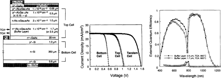
(a) Cross-sectional schematic of 2J AlGaAs/Si solar cell structure, and the corresponding (b) J–V characteristic (AM0) and (c) QE plots, reprinted with permission from Soga et al. (1997). Copyright 1997, Elsevier
Yamaguchi, Nishioka, and Sugo (1989) utilized In0.1Ga0.9As/GaAs SLSs in combination with TCA to significantly minimize the TDD to ~1–2×106 cm−2 for GaAs layers grown on (100) Si substrate by MOCVD. For the growth of 1J GaAs solar cell on Si, (100) Si substrates with 2˚ offcut toward [110] were utilized (Ohmachi et al. 1988). An initial 10- to 15-nm thick low temperature GaAs was grown at 400˚C, followed by the subsequent growth of ~2-µm thick GaAs at 700˚C. Five iterations of TCA were performed at 900˚C, followed by the growth of five periods of In0.1Ga0.9As/GaAs (10 nm/10 nm) SLS and five periods of Al0.6Ga0.4As/GaAs (20 nm/100 nm) SL, prior to the growth of 1J p/n GaAs solar cell structure (Ohmachi et al. 1988; Yamaguchi 2014). The 1J GaAs-on-Si solar cells realized using the combination of TCA, SLS and SL buffer demonstrated an efficiency of 20% under AM1.5g and 18.3% under AM0 conditions (at a TDD of ~4.5×106 cm−2), both of which are the highest efficiencies reported for heteroepitaxial 1J GaAs-on-Si solar cells (Ohmachi et al. 1988; Yamaguchi 2014). The corresponding solar cell structure and the I–V curve are shown in Figure 4(a) and (b), respectively. Further reduction in TDD < 1×106 cm−2, improvement in minority carrier transport properties and thermal mismatch related issues would be essential to enable direct GaAs-on-Si solar cell performance to compete with lattice-matched GaAs-on-GaAs solar cells.

(a) Cross-sectional schematic of 1J GaAs-on-Si solar cell using AlGaAs/GaAs SLs and InGaAs/GaAs SLS (Yamaguch 2014), and (b) the corresponding I–V curve for a 1 cm2 solar cell (Ohmachi et al. 1988), reprinted with permission from Yamaguchi (2014) and Ohmachi et al. (1988). Reference Yamaguchi (2014) Copyright 2014, IEEE; Ohmachi et al. (1988). Copyright 1988, Cambridge University Press.
SixGe1–x graded buffers
GaAs or Ge substrates are currently the conventional choice for commercial multijunction III–V solar cells. One of the inherent benefits of using step-graded SixGe1–x buffer is the ability to realize high-quality, low TDD and relaxed Ge layers on Si substrate providing a “virtual” Ge platform for subsequent GaAs growth (Currie et al. 1998).
Most of the research on SiGe buffers for III–V solar cell integration on Si substrate has been carried out through collaborative research between Ohio State University (OSU) and Massachusetts Institute of Technology (MIT) using combination of growth techniques including ultrahigh vacuum chemical vapor deposition (UHV-CVD), molecular beam epitaxy (MBE) and MOCVD. Typically, the compositionally step-graded 12-µm thick SiGe buffers are grown by UHC-CVD on (100) Si with 6˚ offcut toward <110> plane with final composition ending in 100% Ge (Andre et al. 2005; Lueck et al. 2006). A TDD of ~2.1×106 cm−2 was reported for fully relaxed Ge layers grown on SiGe/Si substrate (Andre et al. 2005; Lueck et al. 2006). For the III–V solar cell growth, an initial epitaxial Ge layer was grown by MBE followed by the growth of GaAs on Ge at an initial low growth temperature using migration-enhanced epitaxy, details of which can be found in Refs (Andre et al. 2005; Sieg et al. 1998). This process has been shown to suppress the formation of APDs due to the controlled nucleation at the GaAs/Ge interface, and etch-pit density of 5×10⁵–2×106 cm−2 was reported for the GaAs layers grown on virtual Ge substrate (Sieg et al. 1998).
Detailed investigation on the impact of TDs on the minority carrier lifetimes revealed superior dislocation tolerance for holes in n-type GaAs (τp~10 ns) in comparison to electrons in p-type GaAs (τn~1.5 ns) material for a similar dislocation density and doping concentration (Carlin et al. 2000; Andre et al. 2004). The reduced electron lifetime was attributed to their higher mobility which translated to increased sensitivity toward the dislocations in GaAs layers grown on metamorphic SiGe buffers (Andre et al. 2004). Such sensitivity of minority carrier lifetime in the metamorphic GaAs material on Ge/SiGe/Si substrates led to superior performance for p+/n diodes over their n+/p counterparts, and hence the p/n solar cell showed higher Voc compared to n/p solar cell (0.98 V vs 0.88 V) at a TDD ~1×106 cm−2, indicating device polarity dependence for metamorphic GaAs solar cells grown on SiGe substrates (Andre et al. 2005; Ringel et al. 2003). Utilizing step-graded SixGe1–x buffer, OSU and MIT teams demonstrated a 1J p/n GaAs solar cell (see Figure 5(a) and (b) for the cell structure and the corresponding cross-sectional TEM image) with an efficiency of 18.1% and 15.5% under AM1.5g and AM0 conditions, respectively (see Figure 6 for the J–V characteristics) (Andre et al. 2005). Such 1J GaAs solar cells on SiGe substrate were demonstrated to exhibit similar performance virtually independent of the cell area, thereby addressing the concern of thermal mismatch related issues between the GaAs epilayers and the Si substrate (Andre et al. 2005). Additionally, Lueck et al. (2006) reported a 2J GaInP/GaAs solar cell on similar Ge/SiGe/Si substrate with an efficiency of 16.8% under AM1.5. The overall performance of the 2J cell was limited by poor antireflection coating, large grid coverage area, significant absorption in the GaAs tunnel junction and due to a lower Voc contribution from the top GaInP subcell (primarily due to a lower top cell bandgap) (Lueck et al. 2006).

(a) Cross-sectional schematic of 1J GaAs solar cell structure grown on Ge/SiGe/Si substrate, and (b) the corresponding cross-section TEM image showing most of the dislocations confined within the buffer layer, reprinted with permission from Andre et al. (2005). Copyright 2005, IEEE
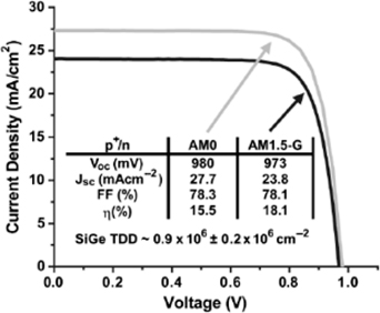
J–V characteristic of 1J p/n GaAs solar cell on Ge/SiGe/Si substrate, reprinted with permission from Andre et al. (2005). Copyright 2005, IEEE
Utilizing a low-bandgap SiGe metamorphic buffer eliminates the possibility of utilizing the bottom Si as a subcell since the SiGe buffer does not provide the optical transparency needed for the bottom Si subcell. Interestingly, Diaz et al. (2014) have utilized an active SixGe1–x cell on the graded SiGe buffer to realize III–V/SiGe tandem solar cell. Both GaAsP and SiGe materials can be compositionally tuned to span a broad range of bandgaps opening possibility for multijunction cells with internal lattice-matching between GaAsP and SiGe. While the unconstrained two-terminal 2J ideal efficiency is 41.7% under AM1.5g for a bandgap combination of 1.73/1.13 eV, the predicted efficiency for 2J GaAsP/SiGe cell is 39.4% (AM1.5g) under lattice-matched conditions (with bandgaps of 1.54/0.84 eV) (Schmieder et al. 2012). Diaz et al. (2014) reported an efficiency of 18.9% under AM 1.5g (Jsc = 18.1 mA/cm2, Voc = 1.45 V and FF = 72%) for 2J GaAs0.84P0.16/Si0.18Ge0.82 (1.67/0.86 eV) tandem solar cell grown on (100)/6˚ offcut Si substrate by a combination of reduced pressure chemical vapor deposition for SiGe buffer and MOCVD for III–V growth. The solar cell structure and the corresponding cross-sectional SEM micrograph are shown in Figure 7(a) and (b), respectively. The corresponding J–V and QE plots for the 2J GaAsP/SiGe tandem solar cell are shown in Figure 8(a) and (b), respectively. The bottom SiGe subcell was found to be current-limiting with significant room for QE improvement in the higher wavelength regime. Further improvements from series resistance minimization, better current-matching and dislocation reduction in the top GaAsP subcell are expected to improve efficiency to ~25% (Diaz et al. 2014). Research efforts at 4Power LLC have led to GaAsP/SiGe tandem solar cells with an efficiency of ~20% (AM 1.5) at a TDD as low as 8×105 cm−2 indicating a promising future for GaAsP/SiGe based tandem solar cells on Si substrate (Pitera et al. 2011).

(a) Cross-sectional schematic of 2J GaAs0.84P0.16/Si0.18Ge0.82 solar cell structure grown on Si substrate, and (b) the corresponding cross-section SEM image, reprinted with permission from Diaz et al. (2014). Copyright 2014, IEEE
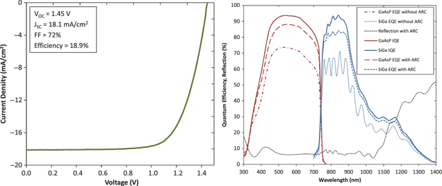
(a) J–V characteristic (AM1.5g) and (b) QE plot of 2J GaAs0.84P0.16/Si0.18Ge0.82 solar cell structure grown on Si substrate, reprinted with permission from Diaz et al. (2014). Copyright 2014, IEEE
GaAsxP1–x graded buffers
A tandem 2J solar cell with a top subcell having a bandgap of 1.7–1.8 eV (GaAs0.7P0.3 being one of the potential candidates) integrated onto a bottom 1.12 eV Si subcell is predicted to have efficiency exceeding of 40% under AM1.5g (Grassman et al. 2012). Furthermore, 3J InGaP/GaAsP//Si (2.0/1.5/1.1 eV) solar cells are expected to achieve >45% efficiency under AM1.5g (Grassman et al. 2012). The large bandgap of GaAsxP1–x buffer provides light transmission to the bottom Si subcell unlike the graded SiGe buffer approach. Geisz et al. (2012) utilized a thin GaP nucleation layer, followed by the growth of lattice-matched GaN0.02P0.98 buffer layer which was compositionally graded using GaAsxP1–x buffer to demonstrate a metamorphic GaAs0.7P0.3 (1.71 eV) solar cell on Si substrate for the first time. 1J GaAs0.7P0.3 solar cell grown on Si substrate by MOCVD was reported with an efficiency of 9.8% (AM1.5g) without antireflection coating. The performance of the solar cell was limited by the high TDD of 9.4×107 cm−2, which translated to a relatively high bandgap-voltage offset, Woc of 0.73 eV (Geisz et al. 2012).
Ringel et al. (2013) and Grassman et al. (2009) have focused efforts on improving the quality of GaP/Si interface to minimize the heterovalent nucleation-related defects, including APDs, stacking faults and microtwins for structures grown by both MBE and MOCVD. Phosphorus diffusion during GaP-on-Si epitaxy was found to be inefficient in forming a diffused emitter to realize an active bottom Si subcell. Hence, n-doped epitaxial silicon emitter was proposed as a more promising alternative. GaP was shown to act as an effective window layer for bottom Si subcell and provided good front surface passivation and minority carrier reflection. Figure 9 shows the 2J GaAsP/Si solar cell structure along with the corresponding cross-sectional TEM image of the MOCVD grown GaAs0.7P0.3 on GaAsP/GaP/Si substrate. A prototype 2J GaAs0.75P0.25/Si solar cell exhibited an efficiency of ~10.65% under AM1.5g spectrum (Jsc = 11.2 mA/cm2, Voc = 1.56 V and FF = 61%) without any antireflection coating (Grassman et al. 2013). The corresponding J–V and QE characteristics are shown in Figure 10(a) and (b), respectively. The overall efficiency was limited by a low FF associated with the GaAs0.75P0.25 tunnel diode, which was inefficient in providing a lossless interconnection between the subcells (Grassman et al. 2013).

(a) Cross-sectional schematic of 2J GaAs0.84P0.16/Si0.18Ge0.82 solar cell structure grown on Si substrate, and (b) the corresponding cross-section SEM image, reprinted with permission from Grassman et al. (2013). Copyright 2013, IEEE

(a) J–V characteristic (AM1.5g) and (b) QE plot of 2J GaAs0.84P0.16/Si0.18Ge0.82 solar cell structure grown on Si substrate, reprinted with permission from Grassman et al. (2013). Copyright 2013, IEEE
More recently, Yaung, Lang, and Lee (2014) have focused efforts on further optimizing the metamorphic GaAsP growth on GaP/Si templates by using MBE. To promote strain relaxation in order to minimize TDD, GaAsP growth temperature was varied from 600 to 700˚C. Authors reported best optimization of rms roughness and TDD at a growth temperature of 600–640˚C. Consequently, improvement in the TDD translated to a low bandgap-voltage offset, Woc~0.55 for GaAs0.77P0.23 (1.66 eV) on GaP/Si templates (TDD ~7.8×106 cm−2) compared to a Woc~0.53 on the GaP substrate. Such GaAsP material with Woc approaching the 0.3–0.4 eV radiative limit represent good material quality for metamorphic 1J GaAsP grown on GaP/Si template. Figure 11(a) shows the cross-sectional schematic of 1J GaAs0.77P0.23 solar cell structure grown on GaP/Si substrate, and the corresponding J–V characteristic (AM1.5g) and the QE plot are shown in Figure 11(b) and (c), respectively. In addition, identical Woc values were reported for both n+/p and p+/n polarities for 1J GaAsP solar cells on GaP/Si template (unlike for the 1J GaAs solar cells on SiGe substrates), suggesting future work should focus efforts on n+/p solar cell designs to take the advantage of GaP as an effective window layer for the bottom Si subcell (Lang et al. 2013). With improvement in the tunnel-junction designs, addition of optimal antireflection coating and further reduction in TDD in the metamorphic GaAsP cells, the future for graded GaAsP buffer approach for integrating III–V/Si tandem solar cell looks very promising.
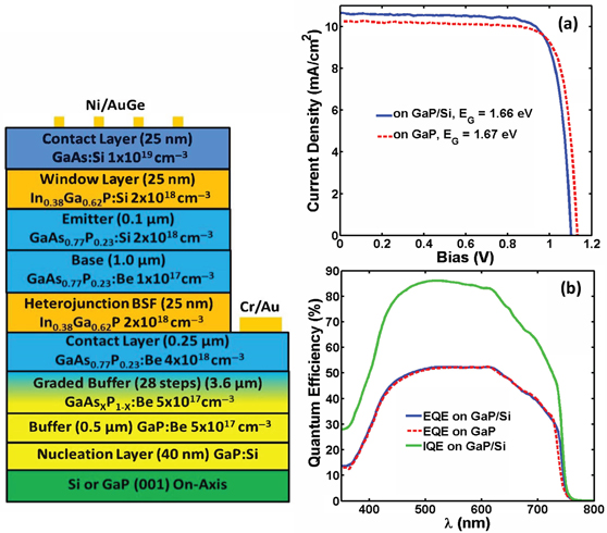
(a) Cross-sectional schematic of 1J GaAs0.77P0.23 solar cell structure grown on GaP/Si substrate, and (b) the corresponding J–V characteristic (AM1.5g) and (c) the QE plot for the 1J GaAs0.77P0.23 solar cell structure grown on GaP vs GaP/Si substrate, reprinted with permission from Yaung, Lang, and Lee (2014). Copyright 2014, IEEE
Dimroth et al. (2014) have utilized metamorphic GaAsxP1–x buffer layer to bridge the lattice constant from Si to GaAs in order to realize conventional 2J GaInP/GaAs solar cells integrated onto inactive Si substrate. A homoepitaxial silicon layer was first grown on (100) Si substrate with 6˚ offcut toward <1–1 1>, followed by the growth of thin GaP nucleation layer. Next, the graded GaAsxP1–x buffer with seven steps was grown at a growth temperature of 640˚C using MOCVD, details of which can found in Ref. Dimroth et al. (2014). A TDD exceeding 108 cm−2 was observed; suggesting future research efforts should focus on utilizing slower grading and growth rates in addition to optimizing the growth temperature for metamorphic GaAsP buffer. An efficiency of 16.4% (Jsc = 11.20 mA/cm2, Voc = 1.94 V and FF = 75.3%) was measured under AM1.5g for the 2J GaInP/GaAs solar cell grown on Si substrate, while the control 2J GaInP/GaAs solar cell grown on GaAs substrate exhibited an efficiency of 27.1%, suggesting that the high TDD was the performance limiting factor for the “on Si” solar cells. An additional important finding was that there was no indication of cracking due to differences in thermal expansion coefficient between Si and GaAs. The QE curve for the 16.4% efficient 2J GaInP/GaAs solar cells realized on GaAsP/GaP/Si substrate is shown in Figure 12. The GaAs subcell was found to be current-limiting due to the reduced minority carrier lifetime associated with high TDD, resulting in inefficient carrier collection in the thick (1.9 µm) GaAs absorbers. Interestingly, the GaInP subcell was less impacted by dislocations due to two possible reasons: (i) additional thermal budget beyond the GaAs subcell growth helped in minimizing the propagation of the dislocations to the top GaInP subcell and (ii) lower thickness (0.79 µm) of the GaInP absorbers did not sufficiently impact the minority carrier collection in spite of a high TDD. Such finding is consistent with dislocation-dependent modeling results for 2J InGaP/GaAs solar cells on Si, wherein the authors reported that lowering the GaInP subcell thickness, allowed increase in the photon flux penetration to the bottom current-limiting GaAs subcell for current-matching (Jain and Hudait 2013). Such tandem 2J InGaP/GaAs solar cells on Si with efficiencies comparable to 2J InGaP/GaAs solar cells on GaAs substrate are possible if TDD lower than106 cm−2 can be achieved (Jain and Hudait 2013). With this approach, 1-sun efficiency in excess of 30% would be realistic for 3J GaInP/GaAs//Si solar cells on Si substrate, offering one of the most promising short-term paths for III–V-on-Si solar cell integration.
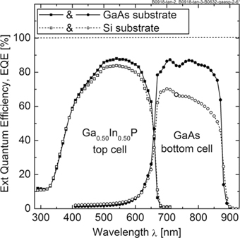
QE plot for 2J InGaP/GaAs solar cell structure grown on GaAs/GaAsP/GaP/Si substrate indicating the bottom GaAs subcell limits the two-terminal current, reprinted with permission from Dimroth et al. (2014). Copyright 2014, IEEE
Lattice-matched III–V–N materials on Si
The biggest advantage of dilute nitride based III–V–N alloys is the ability to grow almost lattice-matched III–V materials on Si substrate for promising III–V/Si tandem solar cells. The quaternary compounds of GaAsxP1–x–yNy and InxGa1–xPyN1–y are attractive options for lattice-matched top subcells in 2J III–V/Si tandem architecture (Almosni et al. 2013). For lattice-matched 3J consideration, the ideal material selection is GaP0.98N0.02 (2 eV)/GaAs0.20P0.73N0.07 (1.5 eV)//Si (1.1 eV) (Almosni et al. 2013). GaAs0.09P0.87N0.04 alloy (bandgap of 1.81 eV) lattice-matched to Si substrate is an attractive top cell choice for 2J III–V/Si tandem solar cell (Almosni et al. 2013). Furthermore, from growth perspective, GaAsPN alloys are easier to grown in comparison to InGaPN due to the difficulties associated with InN and GaN solid-phase miscibility (Korpijärvi et al. 2012; Hsu and Walukiewicz 2008; Ho and Stringfellow 1996).
Geisz et al. (2005) reported the first 2J GaAs0.10 P0.86N0.04 (1.80 eV)/Si tandems solar cell with an efficiency of 5.2% under AM1.5g (without an antireflective coating) utilizing an initial GaP nucleation layer, followed by the MOCVD growth of lattice-matched GaN0.02P0.98 layer. The solar cell structure along with the corresponding I-V and QE characteristic for this tandem solar cell are shown in Figure 13 (a)–(c), respectively. The GaNP layer had a TDD <106 cm−2 with most of the misfit dislocations being confined at the GaP/Si interface. The phosphorus diffusion during the initial GaP growth formed the n-emitter for the p-Si substrate. Intuitively, one would expect the defects at the GaP/Si interface to influence the Si cell response near the front emitter region, however most of the blue light is captured by the top cell and therefore imperfect front passivation did not strongly degrade the Jsc of the Si bottom cell. The top GaAsPN subcell was found to be limiting the two-terminal current (5.7 mA/cm2 for GaAsPN subcell vs 14.5 mA/cm2 for the bottom Si subcell). Furthermore, the unintentional carbon and hydrogen impurities had a strong influence on the minority carrier lifetimes in GaAsPN, resulting in low structural quality of the top nitride subcell which translated to a low tandem cell efficiency. Improving the diffusion lengths in the dilute nitride solar cell material would be pivotal to improve the QE response and hence the overall tandem cell performance. Another important area of attention for the lattice-matched III–V solar cells on Si would be the development of tunnel junction with abrupt interfaces and doping profiles and low series resistance, especially for CPV operation. Recent advancements in dilute nitride materials, GaAsPN/GaPN multiple quantum-well (MQW) structures, extensive research on GaP-on-Si epitaxy and the progress in lattice-matched GaNAsP based lasers on Si (Liebich et al. 2011) present an exciting opportunity to further advance the research on III–V–N based lattice-matched materials on Si for solar cell integration.
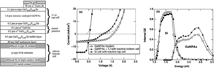
(a) Cross-sectional schematic of lattice-matched 2J GaNPAs/Si solar cell structure grown on Si substrate, (b) J–V characteristic (AM1.5g) and (c) the QE plot of 2J GaN0.04P0.86As0.1/Si solar cell grown on Si substrate, clearly indicating GaNPAs is the current-limiting subcell, reprinted with permission from Geisz et al. (2005). Copyright 2005, IEEE
Lattice-mismatched InGaN-on-Si
With its tunable and direct bandgap spanning the entire useful range of the solar spectrum (0.65 eV – 3.4 eV), InGaN material is one of the most well suited materials for multijunction solar cells. InGaN solar cell with a bandgap of ~1.8 eV would be an ideal candidate for 2J integration with an active 1.1 eV Si bottom subcell. An additional advantage of using InGaN top subcell with Si bottom subcell is the band-alignment of the n-InGaN conduction band with the p-Si valence band which exhibits same energy relative to vacuum, opening a promising option for tunnel junction between the two subcells (Ager et al. 2008). Using simple analytical simulations taking into account realistic diffusion lengths, an efficiency of ~30% (1 sun) is expected for 2J InGaN/Si p/n solar cell, while 3J InGaN (1.9 eV)/InGaN (1.5 eV)/Si solar cell are predicted to be exhibited efficiency of ~35% (1 sun) (Hsu and Walukiewicz 2008). The grading of the InGaN absorber layer close to the top heterointerface (p-GaN/n-InGaN) in a p/n InGaN/Si tandem solar cell is expected to boost the performance as it removes the barrier for hole transport (Brown et al. 2010).
The first experimental evidence of a tandem GaN/Si solar cell was demonstrated using GaN/AlN-buffer/Si 2J p/n solar cell (Lothar et al. 2009). More recently, Tran et al. (2012) demonstrated good quality In0.4Ga0.6N films grown on GaN/AlN/Si(111) substrate with negligible phase separation using high-low-high-temperature AlN-buffer layers by MOCVD. Utilizing a similar growth approach, 1J n-In0.4Ga0.6N/p-Si heterostructure solar cell with enhanced Jsc was demonstrated, attributed to the use of indium tin oxide as the top n-type contact (Tran et al. 2012). A conversion efficiency of 7.12% under AM1.5g (Tran et al. 2012) was achieved, indicating a promising start for InGaN solar cells on Si substrate.
Poor structural quality of nitride materials (especially for InGaN material with >30% indium content) and the associated challenges for p-type doping have been the major impediments in the realization of high-efficiency InGaN solar cells. Large lattice-mismatch between InN and GaN causes a solid-phase miscibility gap due to the low solubility between these two materials (Hsu and Walukiewicz 2008; Ho and Stringfellow 1996). The difficulty in doping InN material with p-type dopant is presumably due to the compensation by native defects. Utilizing p-GaN/n-InxGa1–xN heterojunction is one of the ways to avoid the use of p-doped InxGa1–xN material, wherein the GaN layer also serves as a window layer and reduces the surface recombination (Brown et al. 2010). However, theoretical efficiency of such GaN/InGaN heterojunction is limited to 11% for 1J devices due to the polarization effects, which impede the carrier collection (Fabien et al. 2014). Hence, homojunction devices would be essential to achieve higher efficiencies because employing p-i-n structures could eliminate the polarization effects. Homojunction In0.60Ga0.40N p-n junctions with optimal device designs are predicted to be 21.5% efficiency under AM1.5g conditions (Feng et al. 2013). InGaN based p-i-n solar cells with InGaN as the intrinsic layer between GaN and with graded indium composition up to 50% could lead to theoretical efficiency of 18.53% under AM1.5 (Mahala et al. 2013). InGaN homojunctions with indium-rich, highly p-doped and thick bulk layers with no phase separation would be essential for the success of InGaN solar cells (Fabien et al. 2014). Utilizing metal modulated epitaxy (MME), wherein the metal shutters are modulated with a fixed duty cycle under constant nitrogen flux, is a promising approach. This technique allows for control of the kinetics of Mg incorporation, while using low substrate temperature for growth, thus offering great potential to overcome both p-type doping and phase-separation limitations in In-rich InGaN. InGaN material with up to 66% In content, good crystallinity and rms roughness of 0.76 nm was demonstrated using this MME growth approach (Fabien et al. 2014). Further development of high-quality In-rich InGaN material would be crucial for realizing InGaN/Si tandem solar cells in the future.
Table 2 summarizes the key merits and technological challenges for the respective heteroepitaxial integration approaches for III–V-on-Si solar cells.
Summary of heteroepitaxial III-V-on-Si integration approaches
| Path | Merits | Challenges | Best efficiency |
| GaAsP Graded Buffer | • Start with lattice-matched GaP layer • GaP buffer could serve as a window layer for the bottom Si cell • Possibility for no N- or Al-containing alloys • Semi-transparent buffer for bottom Si cell |
• Mixed anion As–P complex growth • Thick graded buffer |
2J GaInP/GaAs –16.4% (AM1.5g)(Dimroth et al. 2014) |
| SiGe Graded Buffer | • Low dislocation density • Possibility to use Ge or SiGe as subcell |
• Non-transparent buffer, ruling out bottom Si cell • Thick graded buffer • Ge poses severe thermal mismatch concern |
1J GaAs – 18.1% (AM1.5g)(Andre et al. 2005) &2J GaAsP/SiGe – 18.9% (AM1.5g) (Diaz et al. 2014) |
| InGaN-on-Si | • InGaN material composition can span the entire useful solar spectrum • Avoid the need for As, P or Al based materials • Semi-transparent buffer for bottom Si cell |
• Large lattice-mismatch between InGaN and Si • Realization of In-rich InGaN bulk material (In >40%) challenging • Difficulty in p-doping of In-rich InGaN layers • Problem of phase separation in In-rich InGaN material and InN segregation |
1J InGaN//Si heterostructure – 7.12% (AM1.5g)(Tran et al. 2012) |
| GaAsPN-on-Si | • Only path for lattice-matched multijunction III–V solar cells to Si • Transparent & relatively thinner buffers for bottom Si cell • GaP buffer could serve as a window layer for the bottom Si cell |
• Poor diffusion lengths in dilute nitride materials • Challenging to control composition of quaternary alloys |
2J GaAsPN//Si – 5.2% (AM1.5g) – No ARC (Geisz et al. 2005) |
| Direct GaAs-on-Si SL for GaAs-on-Si | • Direct route for realizing record efficient dilute nitride based lattice-matched 3J cells on GaAs substrate • Path for conventional inverted metamorphic cells • Semi-transparent buffer for bottom Si • Lower dislocation density for SL approach |
• High dislocation density • Might use thick buffers to minimize dislocations in some cases • Multiple thermal-cycle anneals • Growth could involve multiple superlattice period •Shutter sequence during switching could be challenging (e.g. InGaAs/GaAsP) |
2J AlGaAs//Si – 21.2% (AM0)(Soga et al. 1997) & 1J GaAs – 21.3% (AM1.5d, 200 suns)(Vernon et al. 1991)1J GaAs – 20% (AM1.5g) & 18.3% (AM0) (Ohmachi et al. 1988) |
Mechanical stacking approach for integrating III–V materials on Si substrate
Ion-implantation induced layer transfer for Ge/Si templates
In the hydrogen-induced layer transfer technique, Ge wafers were implanted with H+ ions and then bonded to Si substrate through a SiO2 bond layer. The wafer bonding was done before starting the epitaxial cell growth. The bonded pair was then annealed to 250–350˚C under > 1 MPa pressure to enable hydrogen-induced layer splitting which initiates the propagation of microcracks parallel to the Ge surface upon annealing (Zahler et al. 2002).
Archer et al. (2008) utilized such bonded templates fabricated with wafer bonding and ion-implantation induced layer transfer technique to realize 2J GaInP/GaAs solar cells (grown by MOVPE) on Ge/Si template with comparable performance to those grown on epi-ready Ge substrate. For the device grown on Ge/Si template, the Jsc was comparable to the control samples on bulk Ge substrate, however the Voc was slightly lower (1.97–2.08 V vs 2.16 V). The drop in Voc translated to 2J GaInP/GaAs efficiency of 15.5–15.7% (AM1.5d) on Ge/Si template compared to 17.2–19.9% on bulk Ge substrate. The authors attributed the decrease in GaInP bandgap (for the samples grown on Ge/Si template) as one of the main reasons for lower Voc. The decrease in GaInP bandgap was believed to be due to the difference in the Ge substrate miscut used to make the Ge/Si template (Archer et al. 2008). It is not trivial to decouple the contributions from the substrate miscut, the GaInP ordering effect and due to the growth conditions on Ge vs Ge/Si substrates and warrants further investigation. Nonetheless, a key advantage of this technique is its metal-free bonding approach enabling the possibility of subsequent upright epitaxial growths. Metal involved for bonding process could otherwise shadow light penetration in case an active subcell below the bond layer is desired. However the thermal mismatch between Si, Ge, III–V materials and the bond layer could pose potential cracking issues in thin solar cell layers (Dimroth et al. 2014) during the subsequent post-bonding epitaxial growth process. Furthermore, rms roughness of films produced by this approach is ~25 nm, and the ion-implantation induced damage extends to ~200 nm into the film, requiring additional steps for damage recovery and polishing to reduce the surface roughness.
Direct fusion bonding
Tanabe, Watanabe, and Arakawa (2012) demonstrated highly transparent and electrically conductive GaAs/Si heterojunctions using direct fusion bonding technique. Heavily doped (degenerate) layers at both the GaAs and the Si bond interface were found to be critical for realizing ohmic behavior. The p+-GaAs/p+-Si and p+-GaAs/n+-Si combination exhibited ohmic behavior for bonding temperatures as low as 300˚C in ambient air. However, when non-degenerate p-GaAs was used, non-ohmic behavior was observed even for samples bonded at 500˚C. Utilizing the direct fusion bonding process, 2J Al0.1Ga0.9As/Si solar cells were fabricated, wherein the Al0.1Ga0.9As subcell was grown on GaAs substrate by MBE and layer-transferred onto a Si subcell by means of p+-GaAs/n+-Si direct-bonding at 300˚C. The p+-GaAs/n+-Si bond layer also served as the tunnel junction between the two n-on-p subcells. The bonding was followed by the subsequent removal of the GaAs substrate. Figure 14(a) shows the cross-sectional TEM image of a similar direct-bonded p+-GaAs/p+-Si heterointerface. The 2J solar cell demonstrated the highest efficiency for bonded 2J III–V/Si tandem solar cell with an active Si subcell. The performance parameters were ɳ = 25.2 %, Jsc = 27.9 mA/cm2, Voc = 1.55 V and FF = 58% under a 600-nm peaked halogen white light source of 1-sun intensity (100 mW/cm2). The corresponding J–V curve is shown in Figure 14(b). One of the major challenges for this approach is the selection of interfacial layers with appropriate polarity and doping concentration which might restrict the design of solar cell polarity (n/p vs p/n).
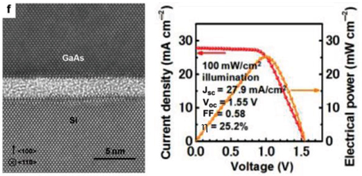
(a) Cross-sectional TEM image of direct-bonded p+-GaAs/p+-Si heterointerface solar cell structure grown on Si substrate, and (b) J–V characteristic of the 2J Al0.1Ga0.9As/Si solar cell realized using direct-bonding, reprinted with permission from Tanabe, Watanabe, and Arakawa (2012). Copyright 2012, Macmillan Publishers
Surface activated direct wafer bonding
Dimroth et al. (2014) and Derendorf et al. (2013) from Fraunhofer ISE demonstrated the use of semiconductor wafer bonding to realize 2J GaInP/GaAs solar cells wafer bonded onto an inactive n-Si wafer as well as 3J GaInP/GaAs//Si solar cells bonded on an active Si solar cell, respectively. This approach is similar to the direct fusion bonding technique. One of the key advantages of this approach is the post-growth wafer bonding which to an extent circumvents the thermal stress caused by difference in thermal expansion coefficient between GaAs and Si, unlike the hydrogen-induced layer transfer technique to realize Ge on Si template (Archer et al. 2008).
The fast beam activated direct wafer bonding process was carried out in an Ayumi SAB-100 system. For the 2J GaInP/GaAs solar cells bonded onto Si substrate (Dimroth et al. 2014), the III–V solar cells were first grown inverted on a GaAs substrate. Thereafter, the GaAs substrate was removed by wet chemical etching, and the bonding was performed at 120˚C. The Si substrate served as an inactive mechanical support and an electrical conductor. The bonded structure was then annealed for 1 minute at 400˚C and processed into 4 cm2 solar cells. This 2J GaInP/GaAs solar cell bonded onto inactive Si substrate demonstrated a conversion efficiency of 26.0% under AM1.5g spectrum with a Voc = 2.39 V, Jsc = 12.7 mA/cm2 and FF = 85.9% (see Figure 15 for the J–V characteristics). The top GaInP subcell was reported to be current-limiting (Jsc = 12.9 mA/cm2 for GaInP subcell vs 14.4 mA/cm2 for the GaAs subcell). With improved current-matched designs, such an approach should be able to achieve greater than 30% efficiency in the future.

J–V characteristic (AM1.5g) of 2J GaInP/GaAs solar cells wafer bonded onto an inactive Si substrate, reprinted with permission from Dimroth et al. (2014). Copyright 2014, IEEE
The 3J GaInP/GaAs//Si solar cells employing an active n–p junction Si solar cell were also realized by the same direct wafer bonding technique at room temperature under a vacuum pressure of 10−6 Pa. The III–V solar cells were grown upright on a GaAs substrate with a degenerately doped n-GaAs bonding layer. Thereafter, the epitaxial structure was stabilized on a sapphire wafer, the GaAs substrate was removed by selective etching, and the cell stack was bonded to the n-doped emitter for the Si subcell. The bonding was initiated by applying a force of 5 kN for a minute. A 4- to 5-nm thin amorphous interface layer was formed by the argon fast atom beam treatment; nonetheless the photovoltaic activity of the Si subcell proved a high transparency of the bond interface. Figure 16(a) and (b) shows the cross-sectional schematic of the solar cell structure and cross-section TEM micrograph of the GaAs–Si bond-layer interface showing the thin amorphous layer. The 3J GaInP/GaAs//Si solar cell was characterized under 1-sun AM1.5d spectrum and demonstrated an efficiency of 20.5% (Jsc = 8.56 mA/cm2, Voc = 2.78 V and FF = 86.3%). The performance of the 3J cell was limited by the low current in the Si subcell due to the low absorption in the indirect bandgap Si substrate. Surface texturing at the back side of the Si substrate and reduction of the III–V layer thicknesses is expected to improve the current-response of the bottom Si subcell. The I–V and QE characteristics of this 3J solar cell are shown in Figure 17(a) and (b), respectively. Under concentrated sunlight, this 3J design demonstrated an efficiency of 23.6% under 71 suns (Bett et al. 2013). At higher concentration, the significant influence of series resistance led to reduction of the FF. The bond interface was attributed as the main contributor to the series resistance which led to the reduced FF under concentrated sunlight. Further optimization of the 3J GaInP/GaAs//Si solar cell has recently led to an efficiency of 27.9% (AM1.5d, 48 suns) (Bett et al. 2013) with headroom for further performance improvement, indicating efficiencies exceeding 30% could be attainable in the near future by employing such a wafer bonding technique for III–V-on-Si solar cell integration.
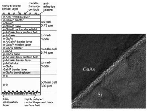
(a) Cross-sectional schematic of 3J GaInP/GaAs//Si solar cell structure grown on Si substrate, and (b) the corresponding cross-section TEM image of the bonded GaAs/Si heterointerface, reprinted with permission from Derendorf et al. (2013). Copyright 2013, IEEE
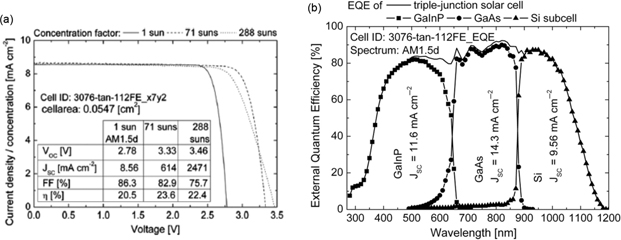
(a) J–V characteristic (AM1.5d) of 3J GaInP/GaAs//Si solar cell under 1 sun and concentrated sunlight, and (b) the corresponding QE plot for the 3J GaInP/GaAs//Si solar cell realized using direct wafer bonding of III–V solar cells onto an active Si subcell, reprinted with permission from Derendorf et al. (2013). Copyright 2013, IEEE
Direct metal interconnect
The direct metal interconnect (DMI) technique is a novel approach where the subcells are fabricated in separate processes and joined mechanically and optically by a transparent epoxy, while the metal-to-metal interconnect provides the electrical contact (Yang et al. 2014). In simple sense, the metal interconnection can be considered to perform the same function as tunnel junctions in conventional multijunction solar cells. DMI technique is capable of providing high tolerance to disparate materials with difference in lattice constants and thermal expansion coefficients, allowing for greater freedom in choosing the subcell materials with optimal bandgap combinations.
Yang et al. (2014) demonstrated a 3J GaInP/GaAs/Si solar cell using the DMI approach. The 2J GaInP/GaAs cells were first grown on lattice-matched Ge substrate, thereafter the substrate was removed using epitaxial lift-off technique, and the metallized front side of the 2J cell was attached to a transparent quartz wafer for support. The bottom side of the 2J solar cell was also metallized to form grid fingers. This structure was then connected to a larger area bottom Si subcell using the DMI technique such that the front grid fingers of the Si solar cell crossed over the bottom grid fingers of the 2J cell, forming a natural cross grid interconnections as shown in Figure 18. An epoxy (Epo-Tek 301–2) covered the non-metallized area and a pressure of ~50 kPa was applied, followed by a subsequent cure at 80˚C for 3 hours. The area of the bottom Si subcell was enlarged to allow sufficient light to reach the bottom Si subcell which typically limits the current in such 3J GaInP/GaAs//Si solar cells. Additionally, in the DMI technique, due to the grid crossover interconnection scheme, the bottom Si subcell experiences significant shading and hence enlarged bottom Si subcell allows for realizing current-matching. Yang et al. referred to this method of using large area for bottom Si substrate compared to the top III–V cells as areal current-matching (ACM). A 3J GaInP/GaAs/Si solar cell with a two-terminal 1-sun efficiency of 25.5% was reported under AM1.5g (Jsc = 11.8 mA/cm2, Voc = 2.74 V and FF = 79%) by employing the ACM technique for an areal Si-to-III–V ratio of 1.16. Figure 19(a) shows the I–V curve of this 3J GaInP/GaAs/Si solar cell. Utilizing the ACM technique, efficiencies exceeding 40% are feasible for 3J GaInP/GaAs/Si solar cells as shown in Figure 19(b). An additional advantage of such tandem cells employing ACM technique is their reduced sensitivity to temporal variations and light non-uniformity. Further improvement in such 3J cells would require antireflection coating at the back side of the III–V cells and alignment of the metal interconnection between the III–V and Si cells to allow maximum light penetration to the bottom Si subcell.
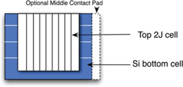
Top-view of 2J GaInP/GaAs solar cell connected to the bottom Si subcell through direct metal interconnection, forming a natural cross grid interconnection, reprinted with permission from Yang et al. (2014). Copyright 2014, IEEE
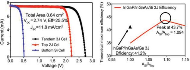
(a) I–V characteristic of 3J GaInP/GaAs/Si solar cell realized using the ACM technique, and (b) AM1.5g theoretical maximum efficiency for of 3J GaInP/GaAs/Si solar cell as function of the areal ratio of the bottom Si subcell with respect to the top two III–V subcells, reprinted with permission from Yang et al. (2014). Copyright 2014, IEEE
Table 3 summarizes the key merits and technological challenges for the respective mechanically stacked integration approaches for III–V-on-Si solar cells.
Summary of mechanically stacked III–V-on-Si integration approaches
| Path | Merits | Challenges | Best efficiency |
| Ion-implantation induced layer transfer | • Metal-free bonding allows for epitaxial growth post-bonding • Post-bonding growth precludes the use of expensive GaAs or Ge substrate |
• Requires hydrogen ion-implantation and results in implantation damages • Pre-growth wafer bonding may impose microcracks issues due to thermal mismatch during high temperature growth • High rms roughness of the transferred layer • Ge layer would make the use of bottom Si subcell challenging |
2J GaInP/GaAs on Ge/Si template – 15.7% (AM1.5d) (Archer et al. 2008) |
| Direct fusion bonding | • Electrically conductive bond layer • Optically transparent bond layer • Post-growth wafer bonding minimizes the thermal stress |
• Requires degenerate semiconductors at the bond interface with specific polarities • Relatively higher bonding temperatures • Formation of thin amorphous layer at the bonding interface |
2J AlGaAs//Si – 25.2% (100 mW/cm2) (Tanabe, Watanabe, and Arakawa 2012) |
| Surface activated direct wafer bonding | • Post-growth wafer bonding minimizes the thermal stress • Low-temperature bonding process • Transparent bond interface |
• Formation of thin amorphous layer at the bonding interface due to Argon fast atom beam • Bond-layer resistance limits performance under high concentration of sunlight |
2J GaInP/GaAs – 26% (AM1.5g) &3J GaInP/GaAs//Si – 20.5% (AM1.5d, 1 sun)27.9% (AM1.5d, 48 suns) (Dimroth et al. 2014; Derendorf et al. 2013; Bett et al. 2013) |
| DMI | • ACM allows for easier current-matching • Low-temperature metal–metal interconnection process • Low interconnection resistance • Improved sensitivity to temporal variation and non-uniform illumination • Relieves the requirement for bonding epoxy to be conductive |
• Metal interconnection in cross over grid pattern increases the shading for bottom cell • Alignment during the bonding process required for minimizing shading |
3J GaInP/GaAs//Si – 25.5% (AM1.5g) (Yang et al. 2014) |
Future outlook
One of the most promising near-term routes for integration of III–V solar cells on Si substrate would be to create virtual “GaAs-on-Si” substrate for the subsequent growth of state-of-the-art 3J InGaP/GaAs/InGaAsNSb solar cells (which are 44% efficient under 947 suns when grown on GaAs substrate (Sabnis, Yuen, and Wiemer 2012)) which are lattice-matched to GaAs as shown in Figure 20(a). Although this approach would utilize the Si substrate as a passive template, such an approach could leverage commercially available GaAs substrate re-use techniques for additional cost reduction (Shahrjerdi et al. 2012; Tatavarti et al. 2010). However, very high-quality GaAs-on-Si template would be essential which would not only require a low TDD but also be negligibly impacted by thermal mismatch. Successful realization of such virtual GaAs-on-Si template can be very challenging and would require novel buffer architectures which might leverage a combination of existing buffer approaches, but not limited to: (i) direct GaAs growth on Si involving TCA and SLSs, (ii) direct Ge epitaxy on Si, (iii) graded GaAsP buffer and (iv) graded SiGe buffer. Triple-junction solar cells with GaInP/GaAsP/SiGe subcells on an inactive Si substrate utilizing SiGe graded buffer could also be an interesting future path to explore.
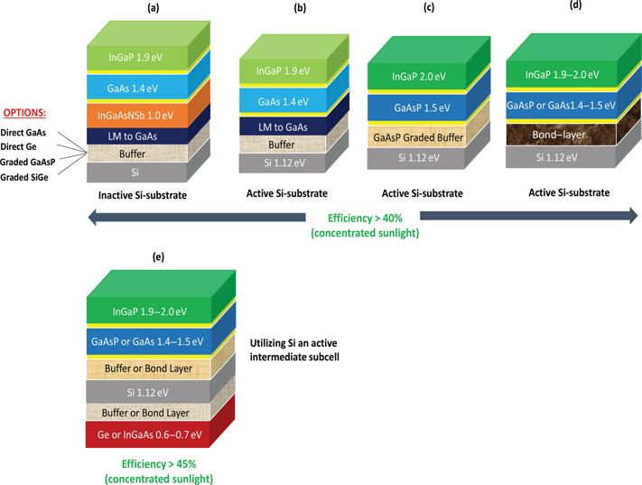
Routes toward high-efficiency III–V-on-Si concentrator solar cells utilizing heteroepitaxial integration approaches are shown in (a)–(c) and by using a combination of heteroepitaxial and mechanical stacking approaches are shown in (d) and (e). Figure 23(a)–(d) represent the most likely path toward >40% efficiency under AM1.5d concentrated sunlight for 3J III–V-on-Si multijunction solar cells, while Figure 20(e) represents the likely path for >45% efficiency utilizing 4J III–V-on-Si multijunction solar cells
When utilizing Si substrate as an active bottom subcell for 3J designs, InGaP or AlGaAs would likely be the preferred top cell material choice, while GaAsP or GaAs would be the preferred middle cell material. The three most promising near-term routes for 3J III–V-on-Si solar cell with an active Si substrate include: (i) 1.9 eV InGaP/1.4 eV GaAs 2J solar cells epitaxially grown on a virtual GaAs-on-Si template with an active Si substrate (see Figure 20(b)), (ii) more ideal bandgap combination could be realized using 2 eV InGaP with 1.5 eV GaAsP on Si using a metamorphic GaAsP buffer (see Figure 20(c)) and (iii) mechanically stacked or wafer bonded 2J InGaP/GaAsP solar cells onto an active bottom Si substrate (see Figure 20(d)). In order for such 3J III–V-on-Si solar cell designs to exceed 40% efficiency (under concentrated sunlight), careful attention needs to be given to dislocation and thermal mismatch management for metamorphic materials on Si, proper tunnel-junction designs (especially for metamorphic GaAsP route) and appropriate bonding layer with optical transparency and good electrical conductivity. Additionally, the bottom Si subcell is likely to be the current-limiting subcell in such designs and would therefore require novel backside substrate engineering to maximize the current density for efficient multijunction designs.
Utilizing III–V-on-Si integration approach, tandem solar cells with four junctions or more would be essential to push the efficiency beyond 45% under concentrated sunlight. If Si substrate were to be used as an active subcell, it would likely require a bottom subcell beneath the Si substrate with a bandgap of ~0.6–0.7 eV (likely to be InGaAs or Ge) as shown in Figure 20(e). Such 4J designs would likely involve a combination of metamorphic epitaxial growth and mechanical stacking.
Conclusions
In summary, III–V multijunction solar cells are regaining attention for integration with Si substrates as a potential solution to address the future LCOE and to unify the high-efficiency merits of III–V materials with the low-cost and abundance of Si. The current state-of-the-art results for III–V-on-Si solar cells are summarized along with the theoretical performance projections for III–V-on-Si solar cell technology. Several routes for integrating III–V materials with Si substrate are discussed. Important design criteria, challenges and trade-offs between the respective buffer schemes are reviewed in relation to minimizing the dislocation density while enabling thin and optically transparent buffers for realizing Si as an active bottom solar cell. Efficient utilization of the bottom Si substrate as an active subcell would require backside Si substrate engineering to enhance the Si subcell current density to realize current-matching condition in III–V/Si tandem solar cells.
Among the heteroepitaxial integration approaches, the realization of virtual GaAs-on-Si templates is likely to be the most promising path to realize near-term high efficiencies; however it is also one of the most challenging paths. Such direct GaAs-on-Si templates could leverage the current state-of-the-art 2J InGaP/GaAs (with active Si subcell) or 3J InGaP/GaAs/InGaAsNSb lattice-matched to GaAs. Although the graded SiGe buffer choice is more effective in terms of dislocation reduction, such buffers are typically very thick and their smaller bandgap would preclude the use of an active bottom Si subcell. The graded GaAsP buffer approach, on the other hand, offers an optically transparent buffer for active bottom Si subcell with optimal bandgap selection for the top and the middle subcell to realize 3J InGaP/GaAsP/Si solar cells. An interesting path combining the SiGe and the GaAsP approach could utilize SiGe as an active subcell to realize 3J InGaP/GaAsP/SiGe solar cells. In the long-run, research on dilute nitride based lattice-matched III–V-N materials on Si and lattice-mismatched InGaN based III–V alloys on Si could also be promising. Among the several mechanical stacking integration approaches, surface activated wafer bonding and DMI techniques are the most promising for near-term success of III–V-on-Si mechanically stacked solar cells. However, one of the key challenges yet to be successfully addressed for mechanically stacked solar cells is the realization of bond layers which are not only optically transparent for an active bottom Si subcell but also electrically conductive to realize efficient two-terminal CPV operation.
Careful consideration of all these design challenges would be very critical for the success of future high-efficiency and low-cost III–V multijunction solar cells on Si substrate. Combination of these different heteroepitaxial and mechanically stacked integration approaches has now opened a new range of possibilities for novel III–V multijunction solar cell architectures on Si substrate. With the recent advancements in both the heteroepitaxial and the mechanically stacked integration approaches, efficiencies exceeding 40% under concentrated sunlight seem achievable for III–V-on-Si multijunction solar cells, indicating a promising future for III–V-on-Si solar cell technology.
Acknowledgment
The authors gratefully acknowledge the funding support in part from the Institute of Critical Research and Applied Sciences (ICTAS) at Virginia Tech.
References
Ager, J. W. , L. A.Reichertz, K. M.Yu, W. J.Schaff, T. L.Williamson, M. A.Hoffbauer, et al. 2008. “InGaN/Si Heterojunction Tandem Solar Cells.” In Proc. 33rd IEEE Photovoltaic Spec. Conf., pp. 1–5.Search in Google Scholar
Al Mansouri, I. , S.Bremner, A.Ho-Baillie, H.Mehrvarz, H.Xiaojing, G.Conibeer, et al. 2013. “Design of Bottom Silicon Solar Cell for Multijunction Devices.” In Proc. 39th IEEE Photovoltaic Spec. Conf., pp. 3310–3314.Search in Google Scholar
Almosni, S. , C.Robert, T.Nguyen Thanh, C.Cornet, A.Létoublon, T.Quinci, et al. 2013. “Evaluation of InGaPN and GaAsPN Materials Lattice-Matched to Si for Multi-Junction Solar Cells.” Journal of Applied Physics113:123509–123509-6.Search in Google Scholar
Andre, C. L. , J. J.Boeckl, D. M.Wilt, A. J.Pitera, M. L.Lee, E. A.Fitzgerald, et al. 2004. “Impact of Dislocations on Minority Carrier Electron and Hole Lifetimes in GaAs Grown on Metamorphic SiGe Substrates.” Applied Physics Letters84:3447–9.Search in Google Scholar
Andre, C. L. , J. A.Carlin, J. J.Boeckl, D. M.Wilt, M. A.Smith, A. J.Pitera, et al. 2005. “Investigations of High-Performance GaAS Solar Cells Grown on Ge-Si1–x-Gex-Si Substrates.” IEEE Transactions on Electron Devices52:1055–60.Search in Google Scholar
Andre, C. L. , D. M.Wilt, A. J.Pitera, M. L.Lee, E. A.Fitzgerald, and S. A.Ringel. 2005. “Impact of Dislocation Densities on N + ∕P and P + ∕N Junction GaAs Diodes and Solar Cells on SiGe Virtual Substrates.” Journal of Applied Physics98:014502–014502-5.Search in Google Scholar
Archer, M. J. , D. C.Law, S.Mesropian, M.Haddad, C. M.Fetzer, A. C.Ackerman, et al. 2008. “GaInP∕GaAs Dual Junction Solar Cells on Ge∕Si Epitaxial Templates.” Applied Physics Letters92:103503–103503-3.Search in Google Scholar
Bett, A. W. , S. P.Philipps, S.Essig, S.Heckelmann, R.Kellenbenz, V.Klinger, M.Niemeyer, D.Lackner, and F.Dimroth. 2013. “Overview about Technology Perspectives for High Efficiency Solar Cells for Space and Terrestrial Applications.” In Proc. 28th European Union-Photovoltaic Solar Energy Conf., pp. 1ap.1.1.Search in Google Scholar
Bolkhovityanov, Y. B. , and O. P.Pchelyakov. 2008. “GaAs Epitaxy on Si Substrates: Modern Status of Research and Engineering.” Physics-Uspekhi51(5):437–56.Search in Google Scholar
Brown, G. F. , J. W.Ager III, W.Walukiewicz, and J.Wu. 2010. “Finite Element Simulations of Compositionally Graded InGaN Solar Cells.” Solar Energy Materials & Solar Cells94:478–83.Search in Google Scholar
Carlin, J. A. , S. A.Ringel, E. A.Fitzgerald, M.Bulsara, and B. M.Keyes. 2000. “Impact of GaAs Buffer Thickness on Electronic Quality of GaAs Grown on Graded Ge/GeSI/Si Substrates.” Applied Physics Letters76:1884–6.Search in Google Scholar
Connolly, J. P. , D.Mencaraglia, C.Renard, and D.Bouchier. 2013. “Designing III-V Multijunction Solar Cells on Silicon.” In Proc. 28th European Union-Photovoltaic Solar Energy Conf.Search in Google Scholar
Currie, M. T. , S. B.Samavedam, T. A.Langdo, C. W.Leitz, and E. A.Fitzgerald. 1998. “Controlling Threading Dislocation Densities in Ge on Si Using Graded SiGe Layers and Chemical-Mechanical Polishing.” Applied Physics Letters72:1718–20.Search in Google Scholar
Derendorf, K. , S.Essig, E.Oliva, V.Klinger, T.Roesener, S. P.Philipps, et al. 2013. “Fabrication of GaInP/GaAs//Si Solar Cells by Surface Activated Direct Wafer Bonding.” IEEE Journal of Photovoltaics3:1423–8.Search in Google Scholar
Diaz, M. , L.Wang, A.Gerger, A.Lochtefeld, C.Ebert, R.Opila, et al. 2014. “Dual-Junction GaAsP/SiGe on Silicon Tandem Solar Cells.” In Proc. 40th IEEE Photovoltaic Spec. Conf.Search in Google Scholar
Dimroth, F. , T.Roesener, S.Essig, C.Weuffen, A.Wekkeli, E.Oliva, et al. 2014. “Comparison of Direct Growth and Wafer Bonding for the Fabrication of GaInP/GaAs Dual-Junction Solar Cells on Silicon.” IEEE Journal of Photovoltaics4:620–5.Search in Google Scholar
D’Souza, S. , J.Haysom, H.Anis, and K.Hinzer. 2011. “The down-to-earth future of Si substrate multi-junction concentrator photovoltaics.” In IEEE Electrical Power and Energy Conf., 57–61.Search in Google Scholar
Fabien, C. A. , M.Moseley, B.Gunning, W. A.Doolittle, A. M.Fischer, Y. O.Wei, et al. 2014. “Simulations, Practical Limitations, and Novel Growth Technology for InGaN-Based Solar Cells.” IEEE Journal of Photovoltaics4:601–6.Search in Google Scholar
Gee, J. M . and G. F.Virshup. 1988. “A 30%-efficient GaAs/silicon mechanically stacked, multijunction concentrator solar cell.” In Proc. 20th IEEE Photovoltaic Spec. Conf., pp. 754–758.Search in Google Scholar
Feng, S. -W. , C. -M.Lai, C. -Y.Tsai, Y. -R.Su, and L. -W.Tu. 2013. “Modeling of InGaN p-N Junction Solar Cells.” Optical Materials Express3:1777–88.Search in Google Scholar
Garcia-Tabares, E. , I.Garcia, D.Martin, and I.Rey-Stolle. 2011. “Optimizing Bottom Subcells for III-V-on-Si Multijunction Solar Cells.” In Proc. 37th IEEE Photovoltaic Spec. Conf., pp. 000784–000789.Search in Google Scholar
Geisz, J. F. , and D. J.Friedman. 2002. “III–N–V Semiconductors for Solar Photovoltaic Applications.” Semiconductor Science and Technology17:769–77.Search in Google Scholar
Geisz, J. F. , J. M.Olson, D. J.Friedman, K. M.Jones, R. C.Reedy, and M. J.Romero. 2005. “Lattice-Matched GaNPAs-on-Silicon Tandem Solar Cells.” In Proc. 31st IEEE Photovoltaic Spec. Conf., pp. 695–698.Search in Google Scholar
Geisz, J. F. , J. M.Olson, M. J.Romero, C. S.Jiang, and A. G.Norman. 2012. “Lattice-Mismatched GaAsP Solar Cells Grown on Silicon by Omvpe.” In Proc. of 4th World Conf. Photovoltaic Energy Conversion, pp. 772–775.Search in Google Scholar
Grassman, T. J. , M. R.Brenner, S.Rajagopalan, R.Unocic, R.Dehoff, M.Mills, et al. 2009. “Control and Elimination of Nucleation-Related Defects in GaP/Si(001) Heteroepitaxy.” Applied Physics Letters94:232106.Search in Google Scholar
Grassman, T. J. , J. A.Carlin, B.Galiana, F.Yang, M. J.Mills, and S. A.Ringel. 2014. “MOCVD-Grown GaP/Si Subcells for Integrated III-V/Si Multijunction Photovoltaics.” IEEE Journal of Photovoltaics4:972–80.Search in Google Scholar
Grassman, T. J. , A. M.Carlin, J.Grandal, C.Ratcliff, L.Yang, M. J.Mills, et al. 2012. “Spectrum-Optimized Si-Based III-V Multijunction Photovoltaics.” In Proc. SPIE 8256, Physics, Simulation, and Photonic Engineering of Photovoltaic Devices, pp. 82560R-82560R-7.Search in Google Scholar
Grassman, T. J. , J. A.Carlin, C.Ratcliff, D. J.Chmielewski, and S. A.Ringel. 2013. “Epitaxially-Grown Metamorphic GaAsP/Si Dual-Junction Solar Cells.” In Proc. 39th IEEE Photovoltaic Spec. Conf., pp. 014900–0153.Search in Google Scholar
Grassman, T. J. , A. M.Carlin, and S. A.Ringel. 2010. “Metamorphic GaAsP and InGaP Photovoltaic Materials on Si for High-Efficiency III-V/Si Multijunction Solar Cells.” In Proc. 35th IEEE Photovoltaic Spec. Conf., pp. 002029–002033.Search in Google Scholar
Green, M. A. 2014. “Silicon Wafer-based Tandem Cells: The Ultimate Photovoltaic Solution?” In Proc. Spie, Physics, Simulation, and Photonic Engineering of Photovoltaic Devices III, pp. 89810L-89810L-6.Search in Google Scholar
Green, M. A. , K.Emery, Y.Hishikawa, W.Warta, and E. D.Dunlop. 2014. “Solar Cell Efficiency Tables (Version 44).” Progress in Photovoltaics: Research and Applications22:701–10.Search in Google Scholar
Ho, I. H. , and G. B.Stringfellow. 1996. “Solid Phase Immiscibility in GaInN.” Applied Physics Letters69:2701–3.Search in Google Scholar
Hsu, L. , and W.Walukiewicz. 2008. “Modeling of InGaN/Si Tandem Solar Cells.” Journal of Applied Physics104:024507–024507-7.Search in Google Scholar
Jain, N. , and M. K.Hudait. 2013. “Impact of Threading Dislocations on the Design of GaAs and InGaP/GaAs Solar Cells on Si Using Finite Element Analysis.” IEEE Journal of Photovoltaics3:528–34.Search in Google Scholar
Jain, N. , and M. K.Hudait. 2014. “Design and Modeling of Metamorphic Dual Junction InGaP/GaAs Solar Cells on Si Substrate for Concentrated Photovoltaic Application.” IEEE Journal of Photovoltaics, 4:1683–1689.Search in Google Scholar
Jain, N. , Y.Zhu, M.Clavel, and M. K.Hudait. 2014. “Performance Evaluation of Monolithically Integrated 3J InGaP/GaAs/Si Tandem Solar Cells for Concentrated Photovoltaics.” In Proc. 40th IEEE Photovoltaic Spec. Conf.Search in Google Scholar
Korpijärvi, V. M. , A.Aho, P.Laukkanen, A.Tukiainen, A.Laakso, M.Tuominen, et al. 2012. “Study of Nitrogen Incorporation into GaInNAs: The Role of Growth Temperature in Molecular Beam Epitaxy.” Journal of Applied Physics112:023504–023504-5.Search in Google Scholar
Kurtz S. R. , P.Faine, and J. M.Olson. 1990. “Modeling of two-junction, series-connected tandem solar cells using top-cell thickness as an adjustable parameter.” Journal of Applied Physics68:1890–1895.Search in Google Scholar
Lang, J. R. , J.Faucher, S.Tomasulo, K.Nay Yaung, and M.Larry Lee. 2013. “Comparison of GaAsP Solar Cells on GaP and GaP/Si.” Applied Physics Letters103:092102–092102-5.Search in Google Scholar
Liebich, S. , M.Zimprich, A.Beyer, C.Lange, D. J.Franzbach, S.Chatterjee, et al. 2011. “Laser Operation of Ga(NAsP) Lattice-Matched to (001) Silicon Substrate.” Applied Physics Letters99:071109–071109-3.Search in Google Scholar
Lothar, A. R. , G.Iulian, Y.Kin Man, M. K.Vincent, W.Wladek, and W. A.Joel. 2009. “III, “Demonstration of a III–Nitride/Silicon Tandem Solar Cell.” Applied Physics Express2:122202.Search in Google Scholar
Lueck, M. R. , C. L.Andre, A. J.Pitera, M. L.Lee, E. A.Fitzgerald, and S. A.Ringel. 2006. “Dual Junction GaInP/GaAs Solar Cells Grown on Metamorphic SiGe/Si Substrates with High Open Circuit Voltage.” IEEE Electron Device Letters27:142–4.Search in Google Scholar
Mahala, P. , A.Ray, O.Jani, and C.Dhanavantri. 2013. “Theoretical Study on the Effect of Graded InyGa1 − yN Layer on p-GaN/InyGa1 − yN/n-GaN p–i–N Solar Cell.” Physica Status Solidi (a)210:2656–61.Search in Google Scholar
Martin, D. , E.Garcia-Tabares, and I.Rey-Stolle. 2013. “Numerical Simulation and Experimental Facts about Bottom-Cell Optimization for III-V on Silicon Multijunction Solar Cells.” In Proc. 39th IEEE Photovoltaic Spec. Conf., pp. 0873–0878.Search in Google Scholar
Mathews, I. , D.O’Mahony, B.Corbett, and A. P.Morrison. 2012. “Theoretical Performance of Multi-Junction Solar Cells Combining III-V and Si Materials.” Optics Express20:A754–A764.Search in Google Scholar
Mitchell, B. , G.Peharz, G.Siefer, M.Peters, T.Gandy, J. C.Goldschmidt, et al. 2011. “Four-junction spectral beam-splitting photovoltaic receiver with high optical efficiency,” Prog. Photovoltaics: Res. Appl. 19:61–72.Search in Google Scholar
Ohmachi, Y. , Y.Kadota, Y.Watanabe, and H.Okamoto. 1988. “High Quality GaAs on Si and Its Application to a Solar Cell.” MRS Online Proceedings Library144:297–302.Search in Google Scholar
Pitera, A. J. , J.Hennessy, A. C.Malonis, E. A.Fitzgerald, and S. A.Ringel. 2011. “Monolithically Integrated Thin Film III-V/Si Solar Panel on Wafer for Active Power Management.” In Proc. 37th IEEE Photovoltaic Spec. Conf., pp. 003703–003706.Search in Google Scholar
Ringel, S. A. , C. L.Andre, M. K.Hudait, D. M.Wilt, E. B.Clark, A. J.Pitera, et al. 2003. “Toward High Performance n/P GaAS Solar Cells Grown on Low Dislocation Density p-Type SiGE Substrates.” In. Proc. of 3rd World Conf. Photovoltaic Energy Conversion, pp. 612–615.Search in Google Scholar
Ringel, S. A. , J. A.Carlin, T. J.Grassman, B.Galiana, A. M.Carlin, C.Ratcliff, et al. 2013. “Ideal GaP/Si Heterostructures Grown by Mocvd: III-V/active-Si Subcells, Multijunctions, and Mbe-to-Mocvd III-V/Si Interface Science.” In Proc. 39th IEEE Photovoltaic Spec. Conf., pp. 3383–3388.Search in Google Scholar
Sabnis, V. , H.Yuen, and M.Wiemer. 2012. “High-Efficiency Multijunction Solar Cells Employing Dilute Nitrides.” AIP Conference Proceedings1477:14–19.Search in Google Scholar
Schmieder, K. J. , A.Gerger, M.Diaz, Z.Pulwin, C.Ebert, A.Lochtefeld, et al. 2012. “Analysis of Tandem III-V/SiGE Devices Grown on Si.” In Proc. 38th IEEE Photovoltaic Spec. Conf., pp. 000968–000973.Search in Google Scholar
Shahrjerdi, D. , S. W.Bedell, C.Ebert, C.Bayram, B.Hekmatshoar, K.Fogel, et al. 2012. “High-Efficiency Thin-Film InGaP/InGaAs/Ge Tandem Solar Cells Enabled by Controlled Spalling Technology.” Applied Physics Letters100:053901-1–053901-3.Search in Google Scholar
Sieg, R. M. , S. A.Ringel, S. M.Ting, S. B.Samavedam, M.Currie, T.Langdo, et al.1998. “Toward Device-Quality GaAS Growth by Molecular Beam Epitaxy on Offcut Ge/Si1 − xGex/Si Substrates.” Journal of Vacuum Science & Technology B16:1471–4.Search in Google Scholar
Soga, T. , K.Baskar, T.Kato, T.Jimbo, and M.Umeno. 1997. “Mocvd Growth of High Efficiency Current-Matched AlGaAs/Si Tandem Solar Cell.” Journal of Crystal Growth174:579–84.Search in Google Scholar
Soga, T. , T.Kato, M.Umeno, and T.Jimbo. 1996. “Photovoltaic Properties of an AlxGa1 − xAs Solar Cell (x=0–0.22) Grown on Si Substrate by Metalorganic Chemical Vapor Deposition and Thermal Cycle Annealing.” Journal of Applied Physics79:9375–8.Search in Google Scholar
Soga, T. , T.Kato, M.Yang, M.Umeno, and T.Jimbo. 1995. “High Efficiency AlGaAs/Si Monolithic Tandem Solar Cell Grown by Metalorganic Chemical Vapor Deposition.” Journal of Applied Physics78:4196–9.Search in Google Scholar
Takano, Y. , M.Hisaka, N.Fujii, K.Suzuki, K.Kuwahara, and S.Fuke. 1998. “Reduction of Threading Dislocations by InGaAs Interlayer in GaAS Layers Grown on Si Substrates.” Applied Physics Letters73:2917–19.Search in Google Scholar
Tanabe, K. , K.Watanabe, and Y.Arakawa. 2012. “III-V/Si Hybrid Photonic Devices by Direct Fusion Bonding.” Science Reports2:349.Search in Google Scholar
Tatavarti, R. , A.Wibowo, G.Martin, F.Tuminello, C.Youtsey, G.Hillier, et al. 2010. “InGaP/GaAs/InGaAs Inverted Metamorphic (IMM) Solar Cells on 4” Epitaxial Lifted off (ELO) Wafers.” In Proc. 35th IEEE Photovoltaic Spec. Conf., 2010, pp. 002125–002128.Search in Google Scholar
Tran, B. -T. , E. -Y.Chang, H. -D.Trinh, C. -T.Lee, K. C.Sahoo, K. -L.Lin, et al. 2012. “Fabrication and Characterization of n-In0.4ga0.6n/p-Si Solar Cell.” Solar Energy Materials & Solar Cells102:208–11.Search in Google Scholar
Umeno, M. , T.Kato, T.Egawa, T.Soga, and T.Jimbo. 1996. “High Efficiency AlGaAs/Si Tandem Solar Cell Over 20%.” Solar Energy Materials & Solar Cells41–42:395–403.Search in Google Scholar
Vernon, S. M. , V. E.Haven, S. P.Tobin, and R. G.Wolfson. 1986. “Metalorganic Chemical Vapor Deposition of GaAS on Si for Solar Cell Applications.” Journal of Crystal Growth77:530–8.Search in Google Scholar
Vernon, S. M. , S. P.Tobin, M. M.Al-Jassim, R. K.Ahrenkiel, K. M.Jones, and B.Keyes. 1990. “Experimental Study of Solar Cell Performance Versus Dislocation Density.” In Proc. 21st IEEE Photovoltaic Spec. Conf., pp. 211–216Search in Google Scholar
Vernon, S. M. , S. P.Tobin, V. E.Haven, C.Bajgar, T. M.Dixon, M. M.Al-Jassim, et al. 1988. “Efficiency Improvements in GaAS-on-Si Solar Cells.” In Proc. 20th IEEE Photovoltaic Spec. Conf., pp. 481–485.Search in Google Scholar
Vernon, S. M. , S. P.Tobin, V. E.Haven, L. M.Geoffroy, and M. M.Sanfacon. 1991. “High-Efficiency Concentrator Cells from GaAs on Si.” In Proc. 22nd IEEE Photovoltaic Spec. Conf., pp. 353–357.Search in Google Scholar
Wilkins, M. M. , A.Boucherif, R.Beal, J. E.Haysom, J. F.Wheeldon, V.Aimez, et al. 2013. “Multijunction Solar Cell Designs Using Silicon Bottom Subcell and Porous Silicon Compliant Membrane.” IEEE Journal of Photovoltaics3:1125–31.Search in Google Scholar
Yamaguchi, M . 1991. “Dislocation Density Reduction in Heteroepitaxial III-V Compound Films on Si Substrates for Optical Devices.” Journal of Materials Research6:376–84.Search in Google Scholar
Yamaguchi, M . 2014. “Potential and Present Status of III-V/Si Tandem Solar Cells.” In Proc. 40th IEEE Photovoltaic Spec. Conf.Search in Google Scholar
Yamaguchi, M. , T.Nishioka, and M.Sugo. 1989. “Analysis of Strained‐Layer Superlattice Effects on Dislocation Density Reduction in GaAs on Si Substrates.” Applied Physics Letters54:24–6.Search in Google Scholar
Yamaguchi, M. , A.Yamamoto, M.Tachikawa, Y.Itoh, and M.Sugo. 1988. “Defect Reduction Effects in GaAs on Si Substrates by Thermal Annealing.” Applied Physics Letters53:2293–5.Search in Google Scholar
Yamane, K. , N.Urakami, H.Sekiguchi, and A.Wakahara. 2014. “III-V-N Compounds for Multi-Junction Solar Cells on Si.” In Proc. 40th IEEE Photovoltaic Spec. Conf.Search in Google Scholar
Yang, J. , Z.Peng, D.Cheong, and R.Kleiman. 2014. “Fabrication of High-Efficiency III-V on Silicon Multijunction Solar Cells by Direct Metal Interconnect.” IEEE Journal of Photovoltaics4:1149–55.Search in Google Scholar
Yaung, K. N. , J. R.Lang, and M. L.Lee. 2014. “Towards High Efficiency GaAsP Solar Cells on (001) GaP/Si.” In Proc. 40th IEEE Photovoltaic Spec. Conf.Search in Google Scholar
Zahler, J. M. , C. -G.Ahn, S.Zaghi, H. A.Atwater, C.Chu, and P.Iles. 2002. “Ge Layer Transfer to Si for Photovoltaic Applications.” Thin Solid Films403–404:558–62.Search in Google Scholar
©2014 by De Gruyter
Articles in the same Issue
- Frontmatter
- III–V Multijunction Solar Cell Integration with Silicon: Present Status, Challenges and Future Outlook
- Monolithic Integration of Diluted-Nitride III–V-N Compounds on Silicon Substrates: Toward the III–V/Si Concentrated Photovoltaics
- Study of the Growth and Dislocation Blocking Mechanisms in InxGa1−xAs Buffer Layer for Growing High-Quality In0.5Ga0.5P, In0.3Ga0.7As, and In0.52Ga0.48As on Misoriented GaAs Substrate for Inverted Metamorphic Multijunction Solar Cell Application
- Organic, Flexible, Polymer Composites for High-Temperature Piezoelectric Applications
- Modeling of a Bridge-Shaped Nonlinear Piezoelectric Energy Harvester
- Enhanced Vibration Energy Harvesting Through Multilayer Textured Pb(Mg1/3Nb2/3)O3–PbZrO3–PbTiO3 Piezoelectric Ceramics
- Load-Tolerant, High-Efficiency Self-Powered Energy Harvesting Scheme Using a Nonlinear Approach
- Comparative Analysis of One-Dimensional and Two-Dimensional Cantilever Piezoelectric Energy Harvesters
- Modeling of Hybrid Piezoelectrodynamic Generators
- Opto-electrical Behavior of Pb(Zn1/3Nb2/3)O3–Pb0.97La0.03(Zr,Ti)O3 Transparent Ceramics with Varying Defect Structure
- Feasibility Study for Small Scaling Flywheel-Energy-Storage Systems in Energy Harvesting Systems
- Ca0.15Zr0.85O1.85 Thin Film for Application to MIM Capacitor on Organic Substrate
- Erratum to EHS 1 (1–2), 69–78 (2014), A High-Temperature Thermoelectric Generator Based on Oxides
- A Direct Entropic Approach to Uniform and Spatially Continuous Dynamical Models of Thermoelectric Devices