A metamaterial loaded hybrid fractal multiband antenna for wireless applications with frequency band reconfigurability characteristics
-
Ritesh Kumar Saraswat
 and
Mithilesh Kumar
and
Mithilesh Kumar

Abstract
In the present article authors propose the design and analysis of an octagonal shape multiband metamaterial loaded antenna with implementation of hybrid fractal geometry for wireless applications. Multiband features in the antenna structure is realized by applying the slotted and hybrid fractalization of Moore and Koch curve approach in radiating section along with introduction of two metamaterial SRR cells. The frequency band reconfigurability characteristics in proposed design is achieved by placing the PIN diode inside the connecting strip between the central hybrid fractal geometry and feedline. During forward bias condition of PIN diode antenna structure resonates at hepta (seven) band mode at WiMAX (3.5 GHz)/Lower C-band (4.41 GHz)/WLAN (5.4/5.8 GHz)/Lower X-band (8.26 GHz)/Upper X-band (10.48 GHz)/Lower Ku-band (13.35 GHz)/Middle Ku-band (14.42 GHz) wireless standards with S11 ≤ −10 dB. Proposed antenna represent the hexa and hepta band features during reverse bias (OFF-state) and forward bias condition (ON-state) of PIN diode respectively. A stable and consistent radiation patterns, appropriate impedance matching and an acceptable gain are achieved at all the operating frequencies of the proposed antenna.
1 Introduction
1.1 Motivation
In present scenario, metamaterial inspired multiple resonant antenna for various wireless standards have gained more attention for researchers. Previously, many multiband antennas are proposed to cover the limited wireless standards WLAN/WiMAX. The multiband features is created within single design with improved radiation characteristics (Patterns/gain/efficiency/current distribution) is a complicated work. There are so many approaches such as factalization, slotted, metamaterial loading (applying on radiating patch section or ground plane) are available to achieve the multiband phenomenon within single antenna for covering various wireless applications. Recently many researchers are focused to design multiband antenna by applying the fractalization and slotted techniques with metamaterial SRR cell implementation on the radiating part of the design with enhanced radiation characteristics. Additionally, the tunability/switching between the wireless standards is attained by integrating the frequency-band reconfigurability in multiband antenna. The tunability/switching operation of resonant-bands are performed by placing the switching element PIN diode in radiating or ground section of antenna design.
1.2 Related literature survey
Recently the development in the field of multiband technology has grown up progressively to operate at various wireless communication modes. As per concern with practical implementation of such technology, it is mostly implemented in smart phones to fulfil the requirement of multiband operating platform for wireless standards. Several approaches are proposed earlier to design the multiband antenna like as feeding techniques [1], [2], [3], slotted radiating part or ground section [4], [5], [6], [7], [8], [9], metamaterial (SRR/CSRR) loading [10], [11], [12], [13], [14], fractalization [15], etc. to cover the wireless communication standards. By applying the etching slot method in antenna design, the multiple resonant bands are created due to the electric current perturbation effect in structure. In [16], [17], [18], slotted antennas are designed to operate multiple wireless communication applications regarding smartphone and mobile handsets respectively.
Another methodology of metamaterial loading have garnered noteworthy attention in designing of multiple resonating smart antenna due to its specific characteristics like as negative dielectric parameters (permeability and permittivity), negative refractive index, electrically small in size etc. In this concern, many metamaterial inspired multiband antenna have been designed and reported in literature [19], [20], [21], [22], [23], [24], [25]. Xu et al. [19] employed a gain-enhanced resonant antennas with implementation of two-dimensional CSRRs loaded CRLH TL (composite Right/Left-handed transmission line). In [20], a miniaturized single-feed circularly-polarized (CP) antenna design is proposed with insertion of meta-surfaces and meta-resonators. A triple-band single-fed compact antenna with polarization diversity and radiation pattern selectivity is designed based on two-dimensional artificial metamaterial transmission line (TL) [21]. Sharma et al. [22] designed a metamaterial triple band antenna for wireless standards WLAN and WiMAX. In [23], [24], [25], metamaterial SRR implemented multiband antenna were reported to operating at multiple wireless application. Ali et al. [26] proposed a quad band antenna with size miniaturization and bandwidth enhancement by applying the technique of etching slot, fractalization and metamaterial loading. The integration of fractalization and metamaterial loading is implementing in antenna designing process is helpful to enhance the impedance matching, radiation (gain/efficiency/patterns) and multiband characteristics [27], [28], [29]. In [30], fractal antenna is designed with SRR shape ground to achieve the multiband environment for wireless standards. Ahmed et al. [31], design and analysis of fractal antenna with Minkowski island split ring resonator (metamaterial loading) for bandwidth enhancement application. Hu et al. [32], present a metamaterial inspired antenna with miniaturization and gain improvement by introducing of SRR structure ground plane. Rajkumar et al. [33], propose an open split ring resonator (metamaterial SRR) antenna with size compactness about 38.83% to operate at multiple wireless applications. A miniaturized multiband metamaterial inspired antenna with frequency band reconfiguration (with the help of RF switch PIN diode) for wireless applications reported in [34], [35]. In [36], a miniaturized multiband antenna is designed by using of DGS (defected ground structure)/slotted ground approach for WLAN/WiMAX applications. In [37], the DGS (defected ground structure) method is implemented to obtain the multiband nature in antenna for wireless communication bands.
In this paper firstly we mentioned the design analysis of multiband slot antenna loaded with hybrid fractal geometry (radiating section: seven segments of hybrid fractals and three duplications) and metamaterial cell (two rectangular shape SRR) covering the hepta (seven) wireless communication modes at S band WiMAX (3.5 GHz)/Lower C band (4.41 GHz: terrestrial fixed and mobile broadband application)/C band WLAN (5.4/5.8 GHz)/Lower X-band (8.26 GHz: Earth exploration-satellite service ITU region 2)/Upper X band (10.48 GHz: Amateur satellite operating band)/Lower Ku band (13.35 GHz: Radar communication application)/Middle Ku band (14.42 GHz: Geostationary satellite service). The frequency band reconfigurability characteristics in proposed design is achieved by inserting the switching element PIN diode inside the strips connected between Moore curve (fused with centered Koch curve) and feedline. In case of reverse (OFF)/forward bias (ON mode) of PIN diode, proposed design is attained the hexa/hepta resonant band characteristics for wireless standards respectively.
This article is structured as follows: First, the design evolution of hepta band antenna (slotted radiating patch: hybrid fractal segments with metamaterial SRR cells) for wireless applications is discussed. Subsequently, study about the proposed hybrid fractal structure and metamaterial SRR cell is described. Thereafter discussed the effect of hybrid fractal geometry, metamaterial SRR cell and switching states of PIN diode (frequency band reconfigurability) on antenna performance respectively. Finally, fabrication and experimental results are discussed, and compare with simulated ones.
1.3 Novelty
The novelty of proposed design is mentioned as; (i) Fractalization (fusion/hybrid form) with metamaterial SRR cell implementation to achieve the hepta band feature; (ii) frequency band reconfiguration between wireless standards is realize by using the switchable slotted radiating patch approach with the help of switching element (PIN diode), and (iii) Radiation parameters (gain/efficiency/patterns: co and cross polarization mode/current distribution) are discussed and compared the respective proposed antenna parameters with previous published antenna parameters in tabulation form (Table 1). Finally, conclude the outcome of the proposed work.
Performance comparison of projected hybrid fractal metamaterial multiband antenna with existing antennas reported in latest literature.
| Ref. | Year | Antenna size (mm × mm × mm) | Operating bandwidth (%) | Antenna peak gain (dBi) | Antenna radiation efficiency (%) | Resonant bands/modes | Wireless applications/standards (GHz) | Frequency-band reconfigurability features |
|---|---|---|---|---|---|---|---|---|
| [11] | 2013 | 52.6 × 30 × 1 | 47.27/38.88 | −0.56/−0.62 | 89.2/98.1 | 2 | GPS/WLAN (1.5/2.4) | No |
| [7] | 2014 | 40 × 40 × 1.6 | 34.48/18.28/19.96 | 3.97/4.04/3.25 | 3 | WLAN/WiMAX (2.4/3.5/5.8) | No | |
| [5] | 2015 | 56 × 44 × 0.8 | 5.56/5.86/19.34/13.69 | 1.3/2.3/3.5/4.4 | 76.8/80.1/96.6/85.5 | 4 | GPS/WLAN/WiMAX (1.5/2.4/3.5/5.4) | No |
| [12] | 2016 | 48 × 48 × 1.6 | 20.73/15.02/31.96 | 1.64/2.07/4.06 | 66.2/77.15/87.6 | 3 | GPS/WLAN (1.9/2.4/5) | No |
| [13] | 2017 | 19.18 × 22.64 × 1.6 | 2.4/3.2/12.1 | 1.36/1.57/1.83 | 3 | UMTS/ WiMAX/WLAN (2.1/3.45/ 5.43) | No | |
| [14] | 2018 | 32 × 38 × 1.6 | 8/6/5/69.3 | 3.8 (Avg. Gain) | 89% (Avg. Rad. Eff.) | 4 | WLAN/WiMAX/ITU/X band (2.4/3.35/5.8/7.5) | No |
| [9] | 2018 | 40 × 40 × 1.5748 | 15.1/3.45/12.59/3.33/3.25/5.4/16.58 | 3.48/3.02/4.49/4.25/3.59/3.81/5 | 7 | WLAN/WiMAX/PAN/OFDM (2.54/3.48/4.02/4.34/5.1/5.54/6.24) | No | |
| [26] | 2018 | 30 × 24.8 × 1.6 | 3.5/5.01/13.2/5.77 | 1.35/1/1.07/1.75 | 4 | WiMAX/X band (3.1/5.52/7.31/9.72) | No | |
| [35] | 2019 | 44 × 39 × 1.6 | 5.11/7.33/11.70/6.38/12.03/5.62 | 2.72/3.81/2.12/2.78/3.68/4.10 | 41.2/84.7/52.8/69.7/78.8/76.9 | 6 | WLAN/WiMAX/C/X/Ku band (3.3/5.0/5.8/6.6/9.9/15.9) | Yes |
| [25] | 2019 | 35 × 34 × 1.6 | 11.81/4.27/4.29/6.62/3.27/4.22/8.13 | 1.94/2.2/1.66/3.87/3.65/4.06/4.14 | 41.5/48.6/58.1/60.1/84.4/78.7/82.1 | 7 | WLAN/WiMAX/C/X/Ku band (2.4/3/3.5/5/5.8/11.8/13.1) | No |
| Proposed antenna | 29.5 × 22 × 1.6 | 28.48/11.32/41.33/26.82/6.76/8.50/11.79 | 1.98/2.38/2.62/3.91/2.24/3.28/4.11 | 51.25/54.28/59.69/67.82/72.34/79.92/81.64 | 7 | S band WiMAX/Lower C band–terrestrial fixed and mobile broadband application/C band WLAN/Lower X band–Earth exploration-satellite service ITU region 2/Upper X band–Amateur satellite operating band/Lower Ku band–Radar communication application/Middle Ku band–Geostationary satellite service (3.5/4.41/5.8/8.26/10.48/13.35/14.42) | Yes |
2 Antenna design and configuration
This part of paper mentioned the evolution stages of proposed slotted multiband antenna (loaded with metamaterial cell and fused fractal geometry) and respective S-parameter (simulated S11) are illustrated in Figures 1 and 2 respectively. Proposed design is constructed on FR4 dielectric substrate (εr = 4.4, tanδ = 0.02) with compact dimensions of 29.5 × 22 × 1.6 mm3.

Design evolution stages of proposed design.

Simulated S11 of proposed antenna for each design stage.
The multiband and frequency band reconfigurability characteristics in the proposed structure are achieved by using following design configuration stages, design stage-I: during design evolution stage-I, antenna consist an octagonal shape radiating section fed with trapezoidal shape microstrip line covering UWB single resonant mode with impedance bandwidth 10.33 GHz (3.12–13.45 GHz, 124.68%) in simulation mode as illustrated in Figure 1 (stage-I) and Figure 2 respectively.
Design stage-II: In this stage inserting the octagonal shape slot with three duplication sections (six segments) of fused hybrid fractal (first iteration Moore and Koch curve) geometry inside the radiating patch to make the antenna design to resonate at triple band state with operating bandwidth 2.68 GHz (3.94–6.62 GHz, 50.75%), 1.75 GHz (8.22–9.97 GHz, 19.24%) and 0.62 GHz (13.02–14.14 GHz, 8.25%) for C band WLAN, Lower X band and Lower Ku band wireless standards respectively, as represented in Figure 1 (stage-II) and Figure 2. The slotted hybrid fractal formation in radiating part is responsible to create the current perturbation effect in proposed design that drives the multiband (triple) band characteristics.
Design stage-III: Under this design evolution stage, loading the two metamaterial rectangular SRR cells within radiating patch to achieve an additional resonant bands at wireless standards Lower C, WLAN, Lower X and Lower Ku band with impedance bandwidth 0.91 GHz (3.76–4.67 GHz, 21.59%), 1.39 GHz (5.12–6.51 GHz, 23.90%), 2.24 GHz (7.71–9.95 GHz, 25.37%) and 2.56 GHz (12.89–15.45 GHz, 18.07%) respectively (during simulation process), as depicted in Figure 1 (stage-III) and Figure 2. It is observed that the proposed SRR cells are liable to create an additional narrow band (as compared to triple resonant bands in Design stage-II) at Lower C band wireless communication mode because of negative permeability characteristics of metamaterial SRR. The solenoidal conducting current is passing through the rectangular SRR rings and obtain the magnetic response regarding additional resonant band.
Design stage-IV: By placing the seventh section of hybrid fractal geometry in radiating part to obtain the hepta band configuration at resonant bands 3.5, 4.41, 5.4/5.8, 8.26, 10.48, 13.35 and 14.42 GHz for wireless applications WiMAX (2.86–3.81 GHz), Lower C band (4.25–4.76 GHz), WLAN (5.01–7.62 GHz), Lower X-band (7.75–10.15 GHz), Upper X band (10.43–11.16 GHz), Lower Ku band (12.84–13.98 GHz) and Middle Ku band (14.12–15.89 GHz) respectively, as indicated in Figure 1 (stage-IV) and Figure 2. The respective seventh fused fractal structure is adjoined with feedline by using conducting strip line with RF switching element PIN diode inside it (Figure 1: stage-IV) to established the frequency band reconfigurability feature in proposed design. During forward bias mode (ON-state) of PIN diode, the electric current path length is varied (current perturbation) which derive the hepta (seven) band characteristics in proposed design [38], [39], [40].
During design stage-I (Figure 1), a conventional Octagonal-shaped patch antenna is designed cover the single UWB resonant band. To achieve the multiband characteristics in proposed design, a hybrid fractal approach with metamaterial (SRR cells) loading is implemented. In concern of proposed SRR cell, it is noticed that the perimeter of the conducting split rings (Ppe − SRL − 1 and Ppe − SRL − 2) are related with the length (LInt − SRL − 1 and LInt − SRL − 2) and width (WInt − SRL − 1 and WInt − SRL − 2) and expressed in following equations:
Above equations are represent the relation between the perimeter of the conducting split rings (Ppe − SRL − 1 and Ppe − SRL − 2) and guided wavelength (λguw) at the respective operating/resonant frequency (freso). The effective dielectric constant (εeffec) is related with substrate height (hsubst), feedline width (Wfdl) and relative permittivity of substrate (εrp) as indicated in Eq. (3) [38]. As per design evolution stages of proposed design, when introducing the SRR cells in antenna (Design stage-III: Figure 1) an additional resonant band at 4.41 GHz (Lower C band) is achieved as illustrated in Figure 2.
In hybrid fractal metamaterial multiband antenna, multiple modes are excited with application of feedline across the radiating patch with respective to the various resonant bands. The fundamental modes (includes higher order odd modes) and even modes (second and fourth order) are formed across the middle section of slotted hybrid fractal radiating patch area (exhibit high impedance) and SRR cells surface respectively. It is also observable that the odd/even modes are excited along the central radiating part depends upon the application of the high/low impedance source feeding to the proposed structure, respectively. The respective generated even/odd modes are liable to establish the appropriate frequency response for proposed design at various wireless standards.
The characteristics mode theory (CMT) derive the relation between the antenna conductor surface current Jco − sur and characteristic mode currents Jcmc (linear summation formation) as:
where γk is the MWC of the kth characteristic mode [41].
Another observation for ideal conductor surface is that the electric field (because of conductor surface current) is equal and opposite manner to the tangential incident electric field is identified as:
Above equation represent the relation between the source and the field. On solving Eq. (5) with the help of Eq. (4) as:
Above expression is modified (with introduction of dot product and parameter Jw (w is any integer)) as:
The characteristic impedance Zch−im = Re + jXi has real and imaginary terms which are related with radiated and stored energy, respectively.
The orthogonality features is present in characteristic modes and define as [41]:
where,
The value of γk (MWC of the kth characteristic mode) is calculated with the help of Eqs. (7) and (8) as:
Above equation may be represented in matrix form as follows:
where,
The characteristic current column matrix Ich − cl of the conductor surface is written as [41]:
The resultant seven (hepta) modes are excited at WiMAX (3.5 GHz)/Lower C-band (4.41 GHz)/WLAN (5.4/5.8 GHz)/Lower X-band (8.26 GHz)/Upper X-band (10.48 GHz)/Lower Ku-band (13.35 GHz)/Middle Ku-band (14.42 GHz) wireless standards with respective to the various eigen values. Since theses modes are not identical to each other but respective modes commonly allotted to accomplish the hepta wireless communication states. In concern of respective excited resonant modes, the impedance matching is attained by implementation of slotted hybrid metamaterial radiating section in proposed design. The input impedance of antenna is computed by considering the electromagnetic fields present between the radiating patch and ground section. Accordingly, each operating state is generalized by the parallel resonant RLC circuit formation as represented in Figure 3. The expression of equivalent input impedance of proposed design is given in following Eq. (12) [42]:
Where,
N = Number of radiating operating modes,

Equivalent circuit model for proposed hybrid fractal metamaterial multiband antenna.
As per concern with design evolution stage-IV, proposed structure is printed on FR4 dielectric material with electrical size 0.3422λ × 0.2552λ × 0.0186λ (29.5 × 22 × 1.6 mm) at lower resonant frequency of 3.48 GHz exhibit trapezoidal shape microstrip feedline and ground plane, as illustrated in Figure 4. The radiating section of antenna has octagonal shape slot (side length 7.4 mm) with three duplication and seven segments of hybrid fractal geometry (fused form of first iterated Moore and Koch curve) loaded with two rectangular SRR cells, as represented in Figure 4 (a). Proposed metamaterial SRR cell consist two rectangular rings attached commonly at one side and opened at opposite side. The layouts (front, side and back view) of proposed structure is indicated in Figure 3. The optimized parametric values (in mm) of antenna design (Figure 4) are:- LS (substrate length) = 29.5, WS (substrate width) = 22, h (substrate height) = 1.6, LG (ground plane length) = 8, WGR1 (trapezoidal shape ground plane width: lower side) = 22, WGR2 (trapezoidal shape ground plane width: upper side) = 10, SL1 (side length: slotted octagonal shape radiating section–larger) = 8 and SL2 (side length: slotted octagonal shape radiating section–smaller) = 2.

Layouts of proposed structure:
(a) Front view,
(b) Side view,
(c) Back view.
The proposed hybrid fractal metamaterial multiband antenna is simulated with the help of simulator CST Microwave Studio (MWS) [43] by using finite element method. After simulation process, the proposed design is fabricated by using PCB prototype machine. The top and bottom side of fabricated prototype is depicted in Figure 5.

Images of fabricated prototype:
(a) Top view (without diode);
(b) Bottom view (without diode);
(c) Top view (with diode);
(d) Bottom view (with diode).
The DC potential is applied across the metal strip (dimension of 2 × 0.6 mm2) to perform the switching between the biasing states (forward/revers bias) of PIN diode. When the DC potential is applied the PIN diode is in forward bias (ON state); and when the applied potential is absent (zero volt), the diode represent the reverse bias mode (OFF state). The PIN diode, metallic strip and blocking capacitor (100 pF) are arranged in series form and placed between the seventh hybrid fractal geometry and feedline, as illustrated in Figure 4 (a). The blocking capacitor is utilized as an isolator to isolate the RF signal from DC part. In proposed design a beam lead PIN diode model of ALPHA-6355 is implemented to perform the frequency-band reconfigurability characteristics during forward bias (ON state–equivalent to 2.6 Ω resistance) and reverse bias (OFF states–equivalent to 0.081 pF capacitance) when applying the DC potential (0.7 V) [44]. Figure 6 (a) and (b) represents the equivalent circuits modeling of ALPHA-6355 PIN diode during ON and OFF states respectively. This modeling denotes the series form of resistor RCC and fixed value inductor LF under ON state (forward bias), whereas during OFF state (reverse bias) it represents the parallel form of resistor RCC and reactive capacitor CR, in series with fixed value inductor LF as depicted in Figure 6 (a) and (b).

An equivalent circuit of PIN diode during ON/OFF states.
The measurement set-up is establish to obtain the experimental parameters like as radiation patterns, gain and efficiency of proposed antenna with the help of vector network analyzer (VNA) and anechoic chamber as shown in Figure 7. In this setup the far-field radiation pattern of proposed design (AUT–Antenna under test) are achieved by using a horn antenna (reference antenna) with Fraunhofer distance [DF ≫ 2 (Dmax)2/λ0; Dmax–maximum dimensions of AUT and λ0–free space wavelength] from proposed antenna in anechoic chamber [38]. The measured values of E and H plane patterns are retrieved at different resonant frequencies by implementation of step rotation process (rotation step about 5° from 0 to 360° with the help of rotation table) during co/cross polarization mode. Subsequently, another antenna parameter such as reflection coefficient (S-parameter: S11), gain, radiation efficiency and antenna impedance are also measured by using the same setup.

Setup (anechoic chamber with VNA) to measure various radiation parameters of proposed antenna.
As per the observation of simulated and measured S-parameters (S11), the proposed structure is resonant on hepta/hexa band under the forward (ON state)/reverse bias (OFF state) modes of PIN diode respectively (electric current path length is increase/reduces during ON/OFF state), as depicted in Figure 8 and Table 2. Proposed antenna exhibit hepta-band characteristics with S11 < −10 dB impedance bandwidth of about 0.95 GHz (2.86–3.81 GHz, 28.48%), 0.51 GHz (4.25–4.76 GHz, 11.32%), 2.61 GHz (5.01–7.62 GHz, 41.33%), 2.4 GHz (7.75–10.15 GHz, 26.82%), 0.73 GHz (10.43–11.16 GHz, 6.76%), 1.14 GHz (12.84–13.98 GHz, 8.50%) and 1.77 GHz (14.12–15.89 GHz, 11.79%) during simulation process, and about 0.71 GHz (3.01–3.72 GHz, 21.09%), 0.44 GHz (4.28–4.72 GHz, 9.78%), 2.37 GHz (5.11–7.48 GHz, 37.65%), 2.27 GHz (7.81–10.08 GHz, 25.38%), 0.7 GHz (10.44–11.14 GHz, 6.49%), 1.02 GHz (12.92–13.94 GHz, 7.59%) and 1.68 GHz (14.14–15.82 GHz, 11.21%) under measurement mode. It is noticed that the frequency band reconfigurability features of proposed antenna for hepta/hexa wireless standards is achieved by using ON/OFF states of PIN diode, as mentioned in Table 2.
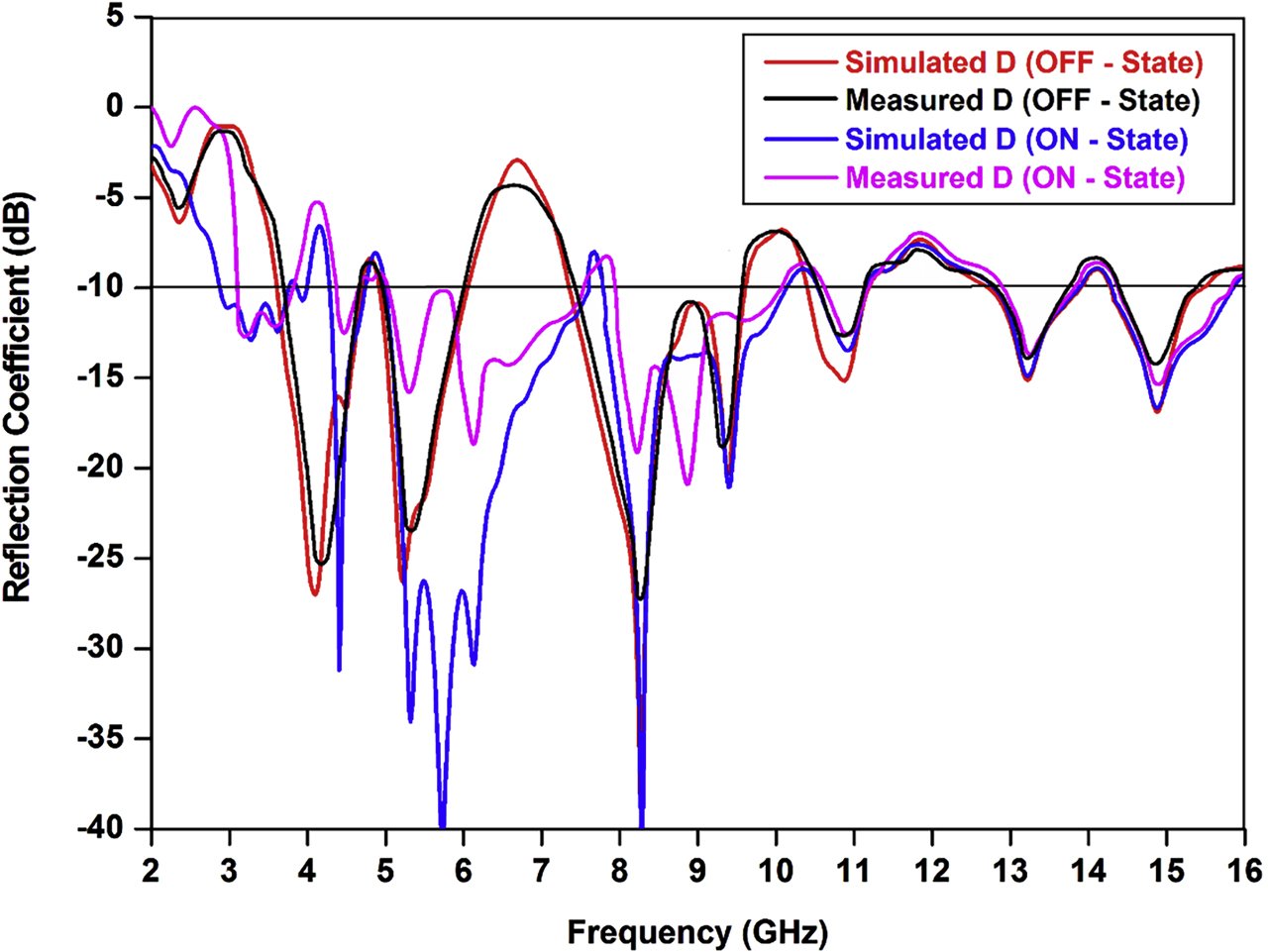
Simulated and measured S11 results during ON/OFF switching states of PIN diode.
Simulated and measured antenna parameters during switching states of PIN diode (Frequency band reconfigurability).
| Diode switching states | Resonating band (in GHz) | 10 dB operating bandwidth (in %) | No. of resonant bands/wireless standards | ||
|---|---|---|---|---|---|
| Sim. | Exp. | Sim. | Exp. | ||
| ON–state (forward bias condition) | 0.95 (2.86–3.81)/0.51 (4.25–4.76)/2.61 (5.01–7.62)/2.4 (7.75–10.15)/0.73 (10.43–11.16)/1.14 (12.84–13.98)/1.77 (14.12–15.89) | 0.71 (3.01–3.72)/0.44 (4.28–4.72)/2.37 (5.11–7.48)/2.27 (7.81–10.08)/0.7 (10.44–11.14)/1.02 (12.92–13.94)/1.68 (14.14–15.82) | 28.48/11.32/41.33/26.82/6.76/8.50/11.79 | 21.09/9.78/37.65/25.38/6.49/7.59/11.21 | Seven (hepta)–bands WiMAX (3.5 GHz)/Lower C band (4.41 GHz: Terrestrial fixed and mobile broadband application)/WLAN (5.4/5.8 GHz)/Lower X-band (8.26 GHz: Earth exploration-satellite service ITU region 2)/Upper X band (10.48 GHz: Amateur satellite operating band)/Lower Ku band (13.35 GHz: Radar communication application)/Middle Ku band (14.42 GHz: Geostationary satellite service) |
| OFF–state (reverse bias condition) | 1.05 (3.63–4.68)/1.14 (4.94–6.08)/2.24 (7.38–9.62)/0.77 (10.42–11.19)/1.11 (12.51–13.62)/1.17 (14.21–15.38) | 0.91 (3.71–4.62)/0.97 (5.01–5.98)/2.09 (7.45–9.54)/0.56 (10.45–11.01)/0.85 (12.63–13.48)/0.94 (14.35–15.29) | 25.27/20.69/26.35/7.13/8.49/7.91 | 21.85/17.65/24.60/5.22/6.51/6.34 | Six (hexa)–bands Lower C band (4.41 GHz: Terrestrial fixed and mobile broadband application)/WLAN (5.4/5.8 GHz)/Lower X-band (8.26 GHz: Earth exploration-satellite service ITU region 2)/Upper X band (10.48 GHz: Amateur satellite operating band)/Lower Ku band (13.35 GHz: Radar communication application)/Middle Ku band (14.42 GHz: Geostationary satellite service) |
2.1 Design and analysis of proposed hybrid fractal geometry
The geometrical structure of proposed radiating hybrid fractal part is obtained by applying the fusion process between the two identical fractal curves (Moore and Koch) as illustrated in Figure 9. The creation of hybrid fractal configuration (fractalization) is depend upon the formation of self-repeating and self-similarity geometrical approach with a constant factor in each iteration stages. The parameters of hybrid fractal structure such as fractal dimension (Dfrd) and length (Lfrt) are achieved with implementation of Iterative Function System (IFS). The respective parameters are calculated using the following equations [45]:
where,
Qsm = Total segments in hybrid fractal geometry,
npr = Total segment partitioning during iteration stages of hybrid fractal geometry,
Tch = Height of fractal curve,
p = Total iteration stages for hybrid fractal geometry.

Fusion process for hybrid fractal structure (fractal curves: first iterated Moore /Koch curve).
The IFS approach is applicable to drive the mathematical analysis of proposed fractal structure. The respective approach is implemented by using affine transformation including the scaling/translation/rotation operations represented in following equations [45];
where
C = Initial geometry matrix for fractal structure,
C1, C2, C3, C4 = Controlling parameters regarding rotation and scaling operation for fractal geometry,
x1, x2 = Coordinating point of vector X,
g1, g2 = Controlling parameters to performing the translation and linear shift operation for fractal geometry,
m = Constant scaling parameter,
θ″ = Angle rotational parameter,
g = Translation parameter for fractal structure.
The proposed hybrid fractal structure is obtained by applying the Hutchinson operator H (C) on the set of transformations for controlling operator ‘C’ as indicated in following Eq. (17) [45];
The designing of proposed hybrid fractal structure is accomplished by using the fusion process between the basic Moore and Koch curve, as depicted in Figure 9. During fusion process first iterated Moore/Koch curve are integrated with each other to create the proposed Moore-Koch Hybrid Fractal Antenna (MKHFA) (Figure 4). In proposed hybrid fractal geometry, Moore and Koch curve are working as an initiator and generator respectively, where generator is superimposed on upward/downward segment of the initiator as illustrated in Figure 9 (a)–(c). Another observation is that the overall length of the conducting radiating part (seven sections of hybrid fractal geometry) is increases about 11.12% by fusion of Koch curve with Moore fractal curve [Figure 4 (a)]. Initially, the length of base curve (Moore Curve: single section) is 28.4 mm without integration of Koch curve and when Koch curve is superimposed on Moore curve the length of base curve is increases upto 31.36 mm. The optimized parametric values (in mm) of proposed hybrid fractal geometry (Figure 3) are:- LMC1 (side length) = 1.15, WMC1 (upper width) = 3, tMC1 (thickness) = 0.25, Wg1 (gap width) = 0.5, LMC2 (side length) = 0.9, WMC2 (upper width) = 2, tMC2 (thickness) = 0.2, Wg2 (gap width) = 0.4, LKC (side length) = 0.75, WKC (width) = 0.8, tKC (thickness) = 0.25 and Wg3 (gap width) = 0.3.
2.2 Design and analysis of proposed metamaterial SRR
This part of paper mentioned the designing and analysis (simulated and measurement mode) of proposed rectangular metamaterial SRR cell. The SRR geometry has two rectangular shape conducting rings with split gap, as illustrated in Figure 10. The S-parameter analysis of proposed SRR cell is achieve by using the waveguide setup in simulation environment (CST Microwave Studio (MWS) simulator) [43] to obtain the simulated reflection parameter (S11: at port 1) and transmission parameter (S21: at port 2) (Figure 10).

Waveguide setup for proposed SRR (simulation environment) with equivalent circuit.
During analysis of SRR cell inside the waveguide setup, implement the waveguide port at the side wall instead of front of the cell (known as the magnetic/electric boundaries or unit-cell boundary condition). As per concern with boundary condition, the waveguide port 1/2, PMC and PEC are allocated for X, Y and Z directions respectively for proposed SRR cell analysis in waveguide setup under simulation mode to retrieve the S-parameters (S11 and S21). The generated electric field (E) is orthogonal with respect to the created magnetic field (H) across the SRR cell within waveguide setup. Another observation is that the magnetic field lines are perpendicular to the SRR plane. The electric field (E) is in parallel and perpendicular direction along the magnetic and electric wall respectively and present across the y-axis at the centre of the waveguide. When applying the excited wave from the source at port 1, the excitation modes are created and present inside the waveguide, and plot the S-parameters (S11 and S21) curves (Simulation mode: with the help of simulator, Experimental mode: with the help of VNA).
The effective permeability μeff/permittivity εeff of proposed SRR cell are retrieved by using the S-parameters S11 and S21 (from the waveguide setup). The measured S-parameters (S11/S21) of proposed SRR are realized with the help of experimental waveguide setup in which the SRR structure is kept inside the waveguide environment attached with two coaxial-to-waveguide adapters (at both ends of waveguide) and VNA (via connecting cable) [46]. The optimized dimensions (in mm) of proposed SRR structure (Figure 4) are:- LSRRE (length of external rectangular SRR ring) = 2.75, WSRRE (width of external rectangular SRR ring) = 8, LSRRI (length of internal rectangular SRR ring) = 2, WSRRI (width of internal rectangular SRR ring) = 6, tSRR (thickness of SRR ring) = 0.25, g (gap width) = 1.4, LSL1 (length of rectangular strip) = 0.75 and WSL1 (width of rectangular strip) = 0.5.
In waveguide setup, during the application of magnetic field on the proposed SRR, an EMF (electro-magnetic field) is created and present across the SRR structure. The generated EMF is coupled with the two conducting rings (rectangular shape) of SRR cell. In this state, conduction current is passing from outer to inner rectangular ring through a distributed capacitance (Capacitive effect: because of ring spacing/gap ‘g’). Therefore, the respective formation (SRR structure) is generating the LC resonant characteristics and provide a specific operating frequency calculated by using the following Eq. (18) [47], [48], [49];
where
Ltot − eqt = Total equivalent inductance of proposed rectangular SRR,
Ctot − eqt = Total equivalent capacitance of proposed rectangular SRR,
LExt − rsrr = Length of external rectangular metallic ring of proposed SRR,
WExt − rsrr = Width of external rectangular metallic ring of proposed SRR,
(g2)rsrr = (g1)rsrr = (g)rsrr = g = Split gap of internal/external rectangular metallic rings of SRR,
(t2)Ext − rsrr = (t1)Ext − rsrr = (t)srr = t = Thickness of internal/external rectangular metallic rings of SRR, δ = Constant parameter (with fixed value = 2.451),
εe = Effective dielectric constant (permittivity) of the medium,
Z0 = Characteristic impedance,
h = height of the conducting strip.
The effective dielectric parameter (permeability: μeff − rsrr) of proposed rectangular SRR can be evaluated by using following Eq. (21) [47], [50];
where
Wave number (kwan) = 2πf/(3 × 108 m/s)
Slab (dielectric substrate material) thickness = Tslt
The comparison between simulated and measured S-parameters (S11: reflection parameter, S21: transmission parameter) of proposed SRR (retrieved from simulated/experimental waveguide setup), as represented in Figure 11. The transmission peak is observed at resonant frequency 4.41 GHz (Figure 11), which can be verified from the theoretical value calculated with the help of Eq. (6). Proposed SRR geometry is identified as a magnetically resonator represents the negative permeability characteristics at operating frequency 4.41 GHz due to the induced magnetic field in perpendicular mode. It is also noticed that the reflection S-parameter (S11) and transmission S-parameter (S21) has about zero level (<−2 dB) and below reference level (−10 dB) respectively at operating frequency 4.41 GHz, which witnesses the stop band features of proposed SRR at this respective resonant frequency. This stop band nature of proposed SRR represent the negative permeability characteristics at resonant frequency 4.41 GHz, as depicted in Figure 12.

Comparison of simulated and measured S11/S21-parameter (retrieved from waveguide setup).

Simulated and measured permeability (real and imaginary mue) curve of proposed SRR.
3 Results
The working mechanism of proposed hybrid fractal metamaterial multiband antenna can be easily define by analysis of current distribution plots at resonant modes 3.5 GHz (WiMAX)/4.41 GHz (Lower C-band)/5.4/5.8 GHz (WLAN)/8.26 GHz (Lower X-band)/10.48 GHz (Upper X-band)/13.35 GHz (Lower Ku-band)/14.42 GHz (Middle Ku-band) as illustrated in Figure 13. At lower resonant frequency mode (wireless standard: WiMAX–3.5 GHz), maximum current distribution is allocated along the periphery of centered seventh hybrid (Moore/Koch) fractal geometry (attached with feedline via strip) as shown in Figure 13. For higher operating frequency mode (wireless standard: Lower C band–4.41 GHz), the concentration of current is maximally focused across the surface of the two SRR cells. Next for higher resonant frequency modes (wireless standard: WLAN–5.4/5.8 GHz, Lower X band–8.26 GHz and Middle Ku band–14.42 GHz), the maximum surface current distribution is exist along the surface of the six hybrid fractal sections (three duplications) in radiating part, which provides the enhanced operating bandwidth with better impedance matching. From Figure 13, it is also noticed that the surface current is exceedingly circulated across the surface of the seventh centered hybrid fractal geometry (connected with feedline via conducting strip) and inner section of octagonal shape slotted radiating section (periphery of six octagonal shape part with hybrid fractal structures, and surface of inner rectangular conducting ring of SRR cells) for higher operating frequency modes 10.48 GHz (upper X band) and 13.35 GHz (Lower Ku band) respectively. Another observation is that the surface current distribution is minimum across the edges of SRR cells/hybrid fractal geometries, and maximum spreads out along the surfaces of various parts (seven hybrid fractal structures/two SRR cells) of radiating patch for all the resonant frequency wireless communication modes, provides the enhanced form of radiation characteristics and bandwidth with improved impedance matching.
![Figure 13: Current distribution analysis (during simulation process: PIN Diode–ON State [48], [49]) for proposed design at various resonant frequency wireless communication modes.](/document/doi/10.1515/freq-2020-0022/asset/graphic/j_freq-2020-0022_fig_013.jpg)
From simulated and measured gain plot of proposed antenna structure, peak gain of 1.98, 2.38, 2.62, 3.91, 2.24, 3.28 and 4.11 dBi (in simulation process), and 1.72, 1.74, 1.98, 2.68, 2.01, 2.98 and 3.79 dBi (during experimental process) are observed at seven (hepta) wireless communication resonant modes 3.5 GHz (WiMAX), 4.41 GHz (Lower C-band), 5.8 GHz (WLAN), 8.26 GHz (Lower X-band), 10.48 GHz (Upper X-band), 13.35 GHz (Lower Ku-band) and 14.42 GHz (Middle Ku-band) respectively as represented in Figure 14.

Simulated and experimental gain plot of projected multiband antenna.
The comparison of simulated and measured radiation efficiency of projected hybrid fractal metamaterial multiband antenna is analyzed in Figure 15. Proposed structure represent the radiation efficiencies 51.25, 54.28, 59.69, 67.82, 72.34, 79.92 and 81.64% (under simulation process) and 44.56, 48.56, 52.76, 59.89, 71.04, 74.89 and 79.12% (during experimental process) at multiple wireless communication resonant bands 3.5 GHz (WiMAX), 4.41 GHz (Lower C-band), 5.8 GHz (WLAN), 8.26 GHz (Lower X-band), 10.48 GHz (Upper X-band), 13.35 GHz (Lower Ku-band) and 14.42 GHz (Middle Ku-band) respectively as depicted in Figure 15.

Comparison of simulated and experimental radiation efficiency against operating frequency range.
To enhance the study about the radiation characteristics of proposed antenna another parameter E & H plane patterns (two dimensional radiation patterns) are analyzed in this section. The principle plane (E & H) patterns (co/cross-polarization states) are observed during simulation and measurement modes, showing a better agreement between these two mode results. The patterns are plotted at distinct operating wireless communication frequencies 3.5 GHz (WiMAX), 4.41 GHz (Lower C-band), 5.8 GHz (WLAN), 8.26 GHz (Lower X-band), 10.48 GHz (Upper X-band), 13.35 GHz (Lower Ku-band) and 14.42 GHz (Middle Ku-band) respectively as indicated in Figure 16. It is observed that, the patterns are arbitrary bidirectional/dipole like and omnidirectional in case of E and H plane (under co-polarization state) respectively, which validate the proposed antenna is most suitable for wireless communication applications. The patterns are achieve the low level of cross polarization (below −15 dB) with stability and consistency at all the operating frequencies.

Two dimensional patterns (E and H plane: co/cross-polarization states) of proposed antenna at 3.5, 4.41, 5.8, 8.26, 10.48, 13.35 and 14.42 GHz.
Table 1 illustrates the performance comparison conducted between the proposed antenna and the existing reported multiband antennas. The projected antenna exhibits seven wireless communication operating bands (with frequency band reconfigurability characteristics), compact dimensions, enhanced bandwidth, acceptable gain and efficiency.
4 Conclusion
In this research article, a hybrid fractal metamaterial loaded hepta band antenna is designed to cover the S band WiMAX (3.5 GHz), Lower C band (4.41 GHz: terrestrial fixed and mobile broadband application), C band WLAN (5.4/5.8 GHz), Lower X (8.26 GHz: band Earth exploration-satellite service ITU region 2), Upper X band (10.48 GHz: Amateur satellite operating band), Lower Ku band (13.35 GHz: Radar communication application) and Middle Ku band (14.42 GHz: Geostationary satellite service) wireless communication applications. The proposed structure exhibit slotted radiating part with seven segments (three duplication sections) of hybrid fractal (Moore-Koch curve) geometry and two rectangular metamaterial SRR cells to achieve the multiple resonant characteristics. Antenna structure also present the frequency band reconfigurability features to obtain the band switching between the wireless standards by implementation of PIN diode within radiating patch. Proposed design has stable and consistent E & H plane patterns (low level of cross polarization), enhanced bandwidth, acceptable gain and efficiency at all the hepta (seven) operating bands of wireless standards. For future work, hybrid fractal approach with multiple fractal curve (2–3 curve) with higher iteration states can be applied to achieve multiband (more than hepta resonant bands) characteristics in the proposed antenna. Since the proposed design has maximum peak gain about 4.11 dBi at 14.42 GHz (Middle Ku-band) during simulation, so the gain can be enhanced by applying the approach of FSS implementation with antenna design.
Acknowledgments
The author thank Prof. S. K. Koul, CARE, IIT Delhi, India, for providing measurement facilities.
Author contribution: Both authors have contributed equally to the work.
Research funding: This research received no specific grant from any funding agency in the public, commercial, or not-for-profit sectors.
Conflict of interest statement: No potential conflict of interest was reported by the authors.
References
[1] D. M. N. Elsheakh, H. A. Elsadek, E. A. F. Abdallah, M. F. Iskander, and H. S. El-Hennawy, “Reconfigurable single and multiband inset feed microstrip patch antenna for wireless communication devices,” Prog. Electromagn. Res. C, vol. 12, pp. 191–201, 2010. https://doi.org/10.2528/pierc10011503.Search in Google Scholar
[2] P. S. Bakariya, S. Dwari, M. Sarkar, and M. K. Mandal, “Proximity-coupled microstrip antenna for bluetooth, WiMAX and WLAN applications,” IEEE Antenn. Wireless Propag. Lett., vol. 14, pp. 755–758, 2015. https://doi.org/10.1109/lawp.2014.2379611.Search in Google Scholar
[3] R. Z. Wu, P. Wang, Q. Zheng, and R. P. Li, “Compact CPW-fed triple band antenna for diversity applications,” Electron. Lett., vol. 51, pp. 735–736, 2015. https://doi.org/10.1049/el.2015.0466.Search in Google Scholar
[4] A. Mehdipour, R. Sebak, C. W. Trueman, and T. A. Denidni, “Compact multiband planar antenna for 2.4/3.5/5.2/5.8-GHz wireless applications,” IEEE Antenn. Wireless Propag. Lett., vol. 11, pp. 144–147, 2012. https://doi.org/10.1109/lawp.2012.2185915.Search in Google Scholar
[5] Y. F. Cao, S. W. Cheung, and T. I. Yuk, “A multiband slot antenna for GPS/WiMAX/WLAN systems,” IEEE Trans. Antenn. Propag., vol. 63, no. 3, pp. 952–958, 2015. https://doi.org/10.1109/tap.2015.2389219.Search in Google Scholar
[6] R. K. Saraswat and M. Kumar, “Frequency band reconfigurable UWB antenna for high gain applications,” Prog. Electromag. Res. B, vol. 64, pp. 29–45, 2015. https://doi.org/10.2528/pierb15090103.Search in Google Scholar
[7] M. Samsuzzaman, T. Islam, N. H. Abd Rahman, M. R. I. Faruque, and J. S. Mandeep, “Compact modified Swastika shape patch antenna for WLAN/WiMAX applications,” Int. J. Antenn. Propag., vol. 2014, pp. 1–8, 2014. https://doi.org/10.1155/2014/825697.Search in Google Scholar
[8] T. Ali, S. Pathan, and R. C. Biradar, “A multiband antenna loaded with metamaterial and slots for GPS/WLAN/WiMAX applications,” Microw. Opt. Technol. Lett., vol. 60, pp. 79–85, 2018. https://doi.org/10.1002/mop.30921.Search in Google Scholar
[9] P. Chaurasia, B. K. Kanaujia, S. Dwari, and M. K. Khandelwal, “Design and analysis of seven-bands-slot-antenna with small frequency ratio for different wireless applications,” AEU Int. J. Electron. Commun., vol. 99, pp. 100–109, 2018. https://doi.org/10.1016/j.aeue.2017.08.057.Search in Google Scholar
[10] J. Zhu and G. V. Eleftheriades, “Dual band metamaterial inspired small monopole antenna for WiFi applications,” Electron. Lett., vol. 45, no. 22, pp. 1104–1106, 2009. https://doi.org/10.1049/el.2009.2107.Search in Google Scholar
[11] H. X. Xu, G. M. Wang, Y. Y. Lv, M. Q. Qi, X. Gao, and S. Ge, “Multi frequency monopole antennas by loading metamaterial transmission lines with dual-shunt branch circuit,” Prog. Electromagn. Res., vol. 137, pp. 703–725, 2013. https://doi.org/10.2528/pier12122409.Search in Google Scholar
[12] T. Alam, M. Samsuzzaman, M. R. I. Faruque, and M. T. Islam, “A metamaterial unit cell inspired antenna for mobile wireless applications,” Microw. Opt. Technol. Lett., vol. 58, no. 2, pp. 263–267, 2016. https://doi.org/10.1002/mop.29543.Search in Google Scholar
[13] S. Daniel, R. Pandeeswari, and S. Raghavan, “A compact metamaterial loaded monopole antenna with offset-fed microstrip line for wireless applications,” AEU Int. J. Electron. Commun., vol. 83, pp. 88–94, 2017. https://doi.org/10.1016/j.aeue.2017.08.030.Search in Google Scholar
[14] M. V. Rao, B. T. P. Madhav, T. Anilkumar, and B. P. Nadh, “Metamaterial inspired quad band circularly polarized antenna for WLAN/ISM/Bluetooth/WiMAX and satellite communication applications,” AEU Int. J. Electron. Commun., vol. 97, pp. 229–241, 2018. https://doi.org/10.1016/j.aeue.2018.10.018.Search in Google Scholar
[15] J. Anguera, C. Puente, C. Borja, and J. Soler, Fractal Shaped Antennas: A Review. Encyclopedia of RF and Microwave Engineering, London, Wiley Interscience, 2005.10.1002/0471654507.eme128Search in Google Scholar
[16] H. D. Chen, H. W. Yang, and C. Y. D. Sim, “Single open-slot antenna for LTE/WWAN smartphone application,” IEEE Trans. Antenn. Propag., vol. 65, no. 8, pp. 4278–4282, 2017. https://doi.org/10.1109/tap.2017.2710228.Search in Google Scholar
[17] S. H. Lee, Y. Lim, Y. J. Yoon, C. B. Hong, and H. I. Kim, “Multiband folded slot antenna with reduced hand effect for handsets,” IEEE Antenn. Wireless Propag. Lett., vol. 9, pp. 674–677, 2010. https://doi.org/10.1109/lawp.2010.2058086.Search in Google Scholar
[18] B. Yuan, Y. Cao, and G. Wang, “A miniaturized printed slot antenna for six-band operation of mobile handsets,” IEEE Antenn. Wireless Propag. Lett., vol. 10, pp. 854–857, 2011. https://doi.org/10.1109/lawp.2011.2165313.Search in Google Scholar
[19] H. X. Xu, G. M. Wang, M. Q. Qi, et al., “Analysis and design of two-dimensional resonant-type composite right/left-Handed transmission lines with compact gain-enhanced resonant antennas,” IEEE Trans. Antenn. Propag., vol. 61, no. 2, pp. 735–747, 2013. https://doi.org/10.1109/tap.2012.2215298.Search in Google Scholar
[20] H. X. Xu, G. M. Wang, J. G. Liang, M. Q. Qi, and X. Gao, “Compact circularly polarized antennas combining meta-surfaces and strong space-filling meta-resonators,” IEEE Trans. Antenn. Propag., vol. 61, no. 7, pp. 3442–3450, 2013. https://doi.org/10.1109/tap.2013.2255855.Search in Google Scholar
[21] H. X. Xu, G. M. Wang, and M. Q. Qi, “A miniaturized triple-band metamaterial antenna with radiation pattern selectivity and polarization diversity,” Prog. Electromagn. Res., vol. 137, pp. 275–292, 2013. https://doi.org/10.2528/pier12081008.Search in Google Scholar
[22] S. K. Sharma, J. D. Mulchandani, D. Gupta, and R. K. Chaudhary, “Triple band metamaterial inspired antenna using FDTD technique for WLAN/WiMAX applications,” Int. J. RF Microw. Comput. Aided Eng., vol. 25, no. 8, pp. 688–695, 2015. https://doi.org/10.1002/mmce.20907.Search in Google Scholar
[23] T. Ali and R. C. Biradar, “A compact multiband antenna using λ/4 rectangular stub loaded with metamaterial for IEEE 802.11 N and IEEE 802.16 E,” Microw. Opt. Technol. Lett., vol. 59, no. 5, pp. 1000–1006, 2017. https://doi.org/10.1002/mop.30454.Search in Google Scholar
[24] J. Kukreja, D. K. Choudhary, and R. K. Chaudhary, “CPW fed miniaturized dual‐band short‐ended metamaterial antenna using modified split‐ring resonator for wireless application,” Int. J. RF Microw. Comput. Aided Eng., vol. 27, no. 8, pp. 1–7, 2017. https://doi.org/10.1002/mmce.21123.Search in Google Scholar
[25] R. K. Saraswat and M. Kumar, “A metamaterial hepta-band antenna for wireless applications with specific absorption rate reduction,” Int. J. RF Microw. Comput. Aided Eng., vol. 29, no. 10, pp. 1–12, 2019. https://doi.org/10.1002/mmce.21824.Search in Google Scholar
[26] T. Ali, M. Saadh Aw, and R. C. Biradar, “A fractal quad-band antenna loaded with L-shaped slot and metamaterial for wireless applications,” Int. J. Microw. Wireless Technol., vol. 10, no. 7, pp. 826–834, 2018. https://doi.org/10.1017/s1759078718000272.Search in Google Scholar
[27] R. Pandeeswari and S. Raghavan, “Broadband monopole antenna with split ring resonator loaded substrate for good impedance matching,” Microw. Opt. Technol. Lett., vol. 56, no. 10, pp. 2388–2392, 2014. https://doi.org/10.1002/mop.28602.Search in Google Scholar
[28] C. Arora, S. S. Pattnaik, and R. N. Baral, “SRR inspired microstrip patch antenna array,” Prog. Electromagn. Res. C, vol. 58, pp. 89–96, 2015. https://doi.org/10.2528/pierc15052501.Search in Google Scholar
[29] V. Rajeshkumar and S. Raghavan, “SRR based polygon ring penta-band fractal antenna for GSM/WLAN/WiMAX/ITU band applications,” Microw. Opt. Technol. Lett., vol. 57, no. 6, pp. 1301–1305, 2015. https://doi.org/10.1002/mop.29070.Search in Google Scholar
[30] C. Elavarasi and T. Shanmuganantham, “Multiband SRR loaded Koch star fractal antenna,” Alex. Eng. J., vol. 57, no. 3, pp. 1549–1555, 2017. https://doi.org/10.1016/j.aej.2017.04.001.Search in Google Scholar
[31] B. H. Ahmed and H. Nrnikman, “Fractal microstrip antenna with Minkowski island split ring resonator for broadband application,” in IEEE International RF and Microwave Conf. 9–11 Dec., Malaysia, IEEE, 2013, pp. 214–218, https://doi.org/10.1109/rfm.2013.6757252.Search in Google Scholar
[32] J. R. Hu and J. S. Li, “Compact microstrip antennas using SRR structure ground plane,” Microw. Opt. Technol. Lett., vol. 56, no. 1, pp. 117–120, 2014. https://doi.org/10.1002/mop.28023.Search in Google Scholar
[33] R. Rajkumar and K. Ushakiran, “A metamaterial inspired compact open split ring resonator antenna for multiband operation,” Wireless Pers. Commun., vol. 97, pp. 951–965, 2017. https://doi.org/10.1007/s11277-017-4545-0.Search in Google Scholar
[34] V. Rajeshkumar and S. Raghavan, “A compact metamaterial inspired triple band antenna for reconfigurable WLAN/WiMAX applications,” Int. J. Electron. Commun., vol. 69, no. 1, pp. 274–280, 2015. https://doi.org/10.1016/j.aeue.2014.09.012.Search in Google Scholar
[35] R. K. Saraswat and M. Kumar, “A vertex-fed hexa-band frequency reconfigurable antenna for wireless applications,” Int. J. RF Microw. Comput. Aided Eng., vol. 29, no. 10, pp. 1–13, 2019. https://doi.org/10.1002/mmce.21893.Search in Google Scholar
[36] R. K. Saraswat and M. Kumar, “Miniaturized slotted ground UWB antenna loaded with metamaterial for WLAN and WiMAX applications,” Prog. Electromagn. Res. B, vol. 65, pp. 65–80, 2016. https://doi.org/10.2528/pierb15112703.Search in Google Scholar
[37] W. C. Liu, C. M. Wu, and Y. Dai, “Design of triple-frequency microstrip-fed monopole antenna using defected ground structure,” IEEE Trans. Antenn. Propag., vol. 59, no. 7, pp. 2457–2463, 2011. https://doi.org/10.1109/tap.2011.2152315.Search in Google Scholar
[38] C. A. Balanis, Antenna Theory: Analysis and Design, 3rd ed., Hoboken, New Jersey, John Wiley, 2005.Search in Google Scholar
[39] A. Naqvi, M. S. Khan, and B. D. Braaten, “A Frequency reconfigurable cylindrically shaped surface with cloaking-like properties,” Microw. Opt. Technol. Lett., vol. 58, no. 6, pp. 1323–1329, 2016. https://doi.org/10.1002/mop.29793.Search in Google Scholar
[40] S. A. Naqvi and M. S. Khan, “Design of a miniaturized frequency reconfigurable antenna for rectenna in WiMAX and ISM frequency bands,” Microw. Opt. Technol. Lett., vol. 60, no. 2, pp. 325–330, 2018. https://doi.org/10.1002/mop.30962.Search in Google Scholar
[41] W. Li, Y. Liu, J. Li, L. Ye, and Q. H. Liu, “Modal proportion analysis in antenna characteristic mode theory,” Int. J. Antenn. Propag., vol. 2019, pp. 1–10, 2019. https://doi.org/10.1155/2019/7069230.Search in Google Scholar
[42] R. Garg, P. Bhartia, I. Bahl, and A. Ittipiboon, Microstrip Antenna Design Handbook, Boston, London, Artech House, 2001.Search in Google Scholar
[43] CST Inc. CST Microwave Studio Suite 2014, Wellesley Hills, Massachusetts, CST Inc., 2014.Search in Google Scholar
[44] Alpha Industries, “ALPHA-6355 beamlead PIN diode,” data sheet, [Online]. Available at: http://www.datasheetarchive.com/ALPHA/PINdiode6355-datasheet.html.Search in Google Scholar
[45] Y. Kumar and S. Singh, “A compact multiband hybrid fractal antenna for multistandard mobile wireless application,” Wireless Pers. Commun., vol. 84, pp. 57–67, 2015. https://doi.org/10.1007/s11277-015-2593-x.Search in Google Scholar
[46] H. Chen, J. Zhang, Y. Bai, et al., “Experimental retrieval of the effective parameters of metamaterials based on a waveguide method,” Opt. Express, vol. 14, no. 26, pp. 12944–12949, 2006. https://doi.org/10.1364/oe.14.012944.Search in Google Scholar PubMed
[47] C. Saha and J. Y. Siddiqui, “Versatile CAD formulation for estimation of the resonant frequency and magnetic polarizability of circular split ring resonators,” Int. J. RF Microw. Comput. Aided Eng., vol. 21, pp. 432–438, 2011. https://doi.org/10.1002/mmce.20533.Search in Google Scholar
[48] H. X. Xu, S. Sun, S. Tang, et al., “Dynamical control on helicity of electromagnetic waves by tunable metasurfaces,” Sci. Rep., vol. 6, p. 27503, 2016, https://doi.org/10.1038/srep27503.Search in Google Scholar PubMed PubMed Central
[49] H. X. Xu, S. Tang, S. Ma, et al., “Tunable microwave metasurfaces for high-performance operations: dispersion compensation and dynamical switch,” Sci. Rep., vol. 6, p. 38255, 2016, https://doi.org/10.1038/srep38255.Search in Google Scholar PubMed PubMed Central
[50] D. R. Smith, S. Schultz, P. Markos, and C. M. Soukoulis, “Determination of negative permittivity and permeability of metamaterials from reflection and transmission coefficients,” Phys. Rev. B, vol. 65, pp. 195104–195109, 2002. https://doi.org/10.1103/physrevb.65.195104.Search in Google Scholar
© 2020 Ritesh Kumar Saraswat and Mithilesh Kumar, published by De Gruyter, Berlin/Boston
This work is licensed under the Creative Commons Attribution 4.0 International License.
Articles in the same Issue
- Frontmatter
- Research Articles
- A concurrent dual-band radar sensor for vital sign tracking and short-range positioning
- Scanning rate enhancement in substrate integrated waveguide periodic leaky wave antenna with continuous beam scanning using delay lines
- Smart DRA for beam width and orientation control
- Multiband planar antenna with CSRR loaded ground plane for WLAN and fixed satellite service applications
- A metamaterial loaded hybrid fractal multiband antenna for wireless applications with frequency band reconfigurability characteristics
- Investigation on two dimensional photonic crystal based two/three input all optical AND gate
- A balanced-to-balanced directional coupler based on branch-slotline coupled structure
- An improved technique for low-loss material complex permittivity and permeability determination from transmission-only measurements