High-power ultrafast thin-disk multipass amplifiers for efficient laser-based manufacturing
-
Marwan Abdou Ahmed

Abstract
Thin-disk multipass amplifiers represent one of the most powerful approaches to scale the average and peak powers of ultrafast laser systems. The present paper presents the amplification of picosecond and femtosecond pulses to average powers exceeding 2 and 1 kW, respectively. Second-harmonic generation in lithium-triborate crystals with powers higher than 1.4 kW and 400 W at a wavelength of 515 nm with picosecond and femtosecond pulse durations, respectively, are also reported. Furthermore, third-harmonic generation was demonstrated with output powers exceeding 250 W at a wavelength of 343 nm. Finally, processing of silicon, metals, and polycrystalline diamond with fs pulses at an average power of 1 kW is presented to demonstrate removal rates that are improved by orders of magnitude as compared to state-of-the-art techniques.
1 Introduction
High-power ultrafast lasers offer a great opportunity for a broad range of scientific and industrial applications such as high-field laser-matter interaction, attoscience, spectroscopy, and control of ultrafast processes and dynamics in semiconductor materials, cutting, drilling, and surface structuring of metals, semiconductors, and dielectrics, welding of transparent materials, surgery, and bio-engineering of organic materials.
At high powers (multi 100 W to multi-kW), the most established laser technologies are based on fiber, slab, and thin-disk architectures [1], [2], [3], [4], [5], [6], [7], [8], [9], [10]. The main achievements with these three technologies at a wavelength of 1 μm are shown in Figure 1 [11].
![Figure 1:
Pulse energy versus repetition rate of state-of-the-art ultrafast amplifier systems based on fiber, slab, and thin-disk architectures and of TD oscillators [11].](/document/doi/10.1515/aot-2021-0047/asset/graphic/j_aot-2021-0047_fig_001.jpg)
Pulse energy versus repetition rate of state-of-the-art ultrafast amplifier systems based on fiber, slab, and thin-disk architectures and of TD oscillators [11].
In this paper, we present our latest achievements of high-power thin-disk multipass amplifiers delivering ultra-short pulses with more than 1 kW of average output power as well as their application to three examplary cases, i.e. processing of silicon and diamond. A brief overview of the results obtained for a second (SHG) and third (THG) harmonic generation is also presented.
2 Thin-disk multipass amplifier: concept
Figure 2 shows the principal setups of the thin-disk multipass amplifiers (TDMPA) for single- and double-pass through the multipass amplifier. The latter can be achieved easily by adding a thin-film polarizer (TFP) at the input of the TDMPA and a combination of a quarter-wave plate and a back-reflection mirror [11] at the end of the optical path through the amplifier. A thin-disk laser crystal with a typical diameter of 15–20 mm, a thickness ranging from 100 to 300 μm, and an Yb doping concentration of 7–11% is used as the amplifying medium. The well-established Yb:YAG or Yb:LuAG is commonly used as an active material for high average powers. Anti-reflection (AR) and high-reflection (HR) coatings for both the pump and the laser radiation are applied on the front and the backside of the crystal, respectively. The thin disk is glued on a polycrystalline diamond (PCD) heat sink and mounted inside a pumping unit which typically allows for 24, 44, or 48 passes of the pump radiation to ensure its efficient (>95%) absorption. The TDMPA scheme is based on a fully passive geometrical folding of the seed laser beam over the thin disk by the use of an array of mirrors facing the disk combined with a set of mirrors and a retro-reflecting mirror pair facing the array. The number of passes through the disk depends on the number of mirrors in the array and typically amounts to between 40 and 100. Arrays of 60 and 80 mirrors are used in the examples presented in Section 3.
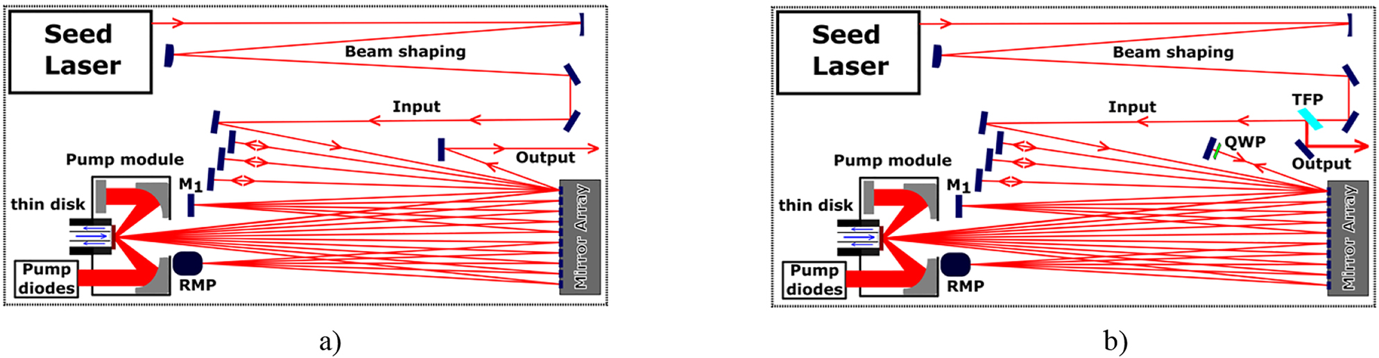
Principal setup of thin-disk multipass amplifiers in (a) single- and (b) double-pass configuration. It is composed of a seed laser, a pump module in which a thin-disk laser-active medium is mounted, an array of mirrors, a number of mirrors (M1) facing the array, and a retro-reflecting mirror pair (RMP).
The use of a collimated seed beam in combination with plane optics (plan mirrors) and a thin-disk with a large radius of curvature (typically >20 m) to avoid tight foci inside the amplifier is a great advantage of this concept as it makes it well-suited for scaling both the average and the peak power. Figure 3 shows the calculated beam propagation through a multipass amplifier composed of an array with 80 mirrors and a disk with a radius of curvature of 20 m. The array and the disk are separated by a distance of 1.2 m. The diameter of the pumped area in the disk and of the collimated incident seed beams are 5.4 and 5 mm, respectively. It can be seen that the smallest diameter of the beam inside the amplifier is larger than 1.8 mm.
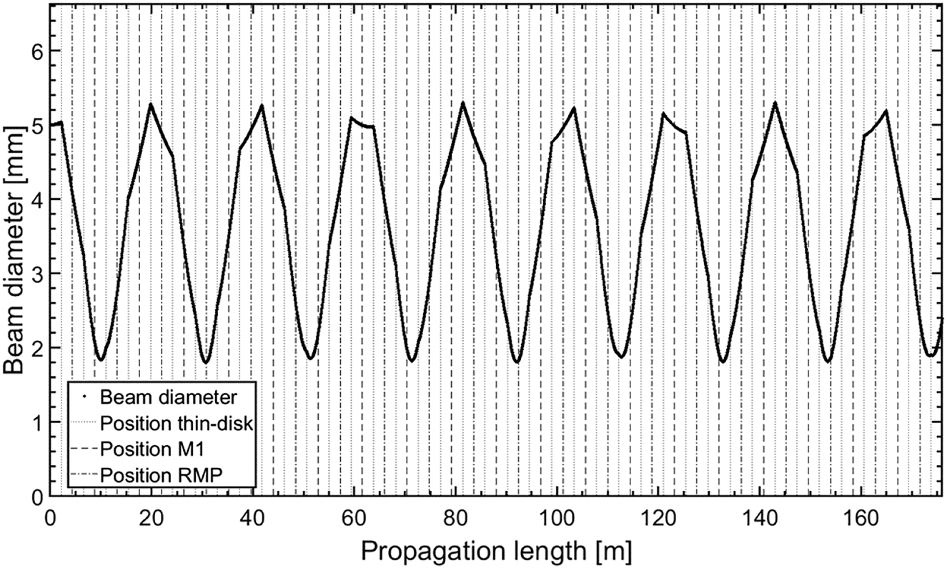
Calculated beam diameter as a function of propagation distance inside a TDMPA with an array of 80 mirrors. A collimated beam with a diameter of 5 mm is injected into the TDMPA. No thermal lens is considered. The beam diameter is varying between 5.3 and 1.8 mm along the propagation.
Thermal lensing caused by the heat load in the thin-disk laser crystal at high average powers plays an important role and has to be taken into account for the design of the TDMPA. By assuming a thermal lens with a focal length of F therm = −21 m (which according to our measurements corresponds to an absorbed pump-power density of approx. 8 kW/cm2 at a wavelength of 969 nm) the beam propagation scheme is slightly modified as shown by Figure 4. The amplitude of the modulation of the beam diameter is reduced and results in a minimum diameter inside the amplifier which is larger than 2.5 mm. This is a further advantage of the present approach for scaling of the peak power and can be further enhanced by using thin disks with larger radii of curvatures (RoC > 50 m).
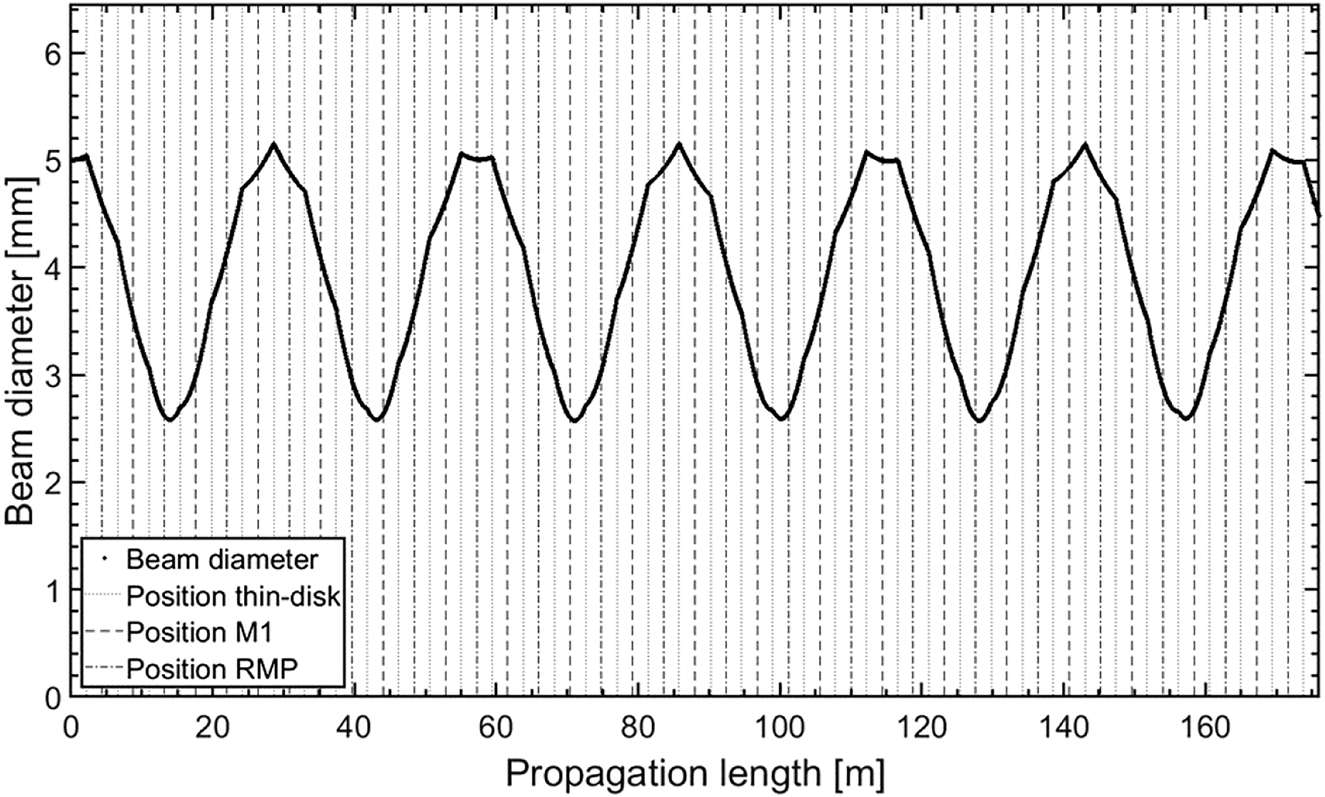
Calculated beam diameter as a function of propagation distance inside the TDMPA with an array of 80 mirrors. A collimated beam with a diameter of 5 mm is injected into the TDMPA. A thermal lens with a focal length of F therm = −21 m is considered. The beam diameter is varying between 5.2 and 2.6 mm along the propagation.
The following section illustrates the capabilities of the thin-disk multipass amplifier concept for the direct amplification of beams with picosecond and femtosecond pulses to average powers of beyond 1 kW and pulse energies of several mJs [12], [13], [14].
3 Thin-disk multipass amplifier: experimental results
3.1 Amplification of picosecond pulses
Figure 5 shows the 2-stage thin-disk multipass amplifier scheme that was used for the experiments reported in [15]. A slightly modified TruMicro 5050 delivering a linearly polarized beam with 6.5 ps long pulses (FWHM) at an average power of 105 W and a repetition rate of 300 kHz was used as a seed laser. The beam quality factor M 2 of this seed beam was measured to be below 1.2. Thin disks of Yb:YAG with a radius of curvature of 20 m, a doping concentration of 10–11%, and thicknesses of approx. 170 and 120 µm were used for the first and the second multipass amplifier, respectively. Single-pass configuration (see Figure 1a) with an array of 60 individually adjustable mirrors was employed in both amplifiers. This allows for a total of 30 reflections of the beam at the HR coated rear side of the thin-disk laser crystal on its path through each of the amplifiers. The thin-disk laser crystals were both pumped at a wavelength of 969 nm i.e. on the zero-phonon line of Yb:YAG. An average output power of 435 W was attained after the first amplifier stage. The overall performance of the two-stage amplifier system is shown in Figure 6a. A maximum output power of 2050 W, corresponding to an extraction efficiency of 44% was achieved. At a repetition rate of 300 kHz, this corresponds to a pulse energy of 6.8 mJ.
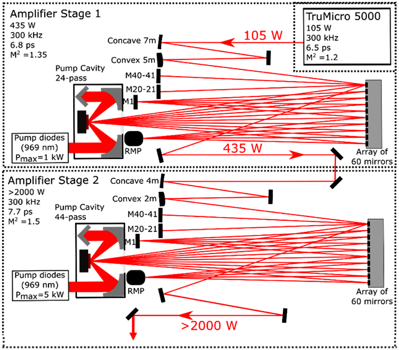
Experimental setup composed of two cascaded thin-disk multipass amplifiers. A slightly modified TruMicro5050 laser delivering 6.5 ps long pulses with an average power of 105 W at a repetition rate of 300 kHz is used as the seed laser.
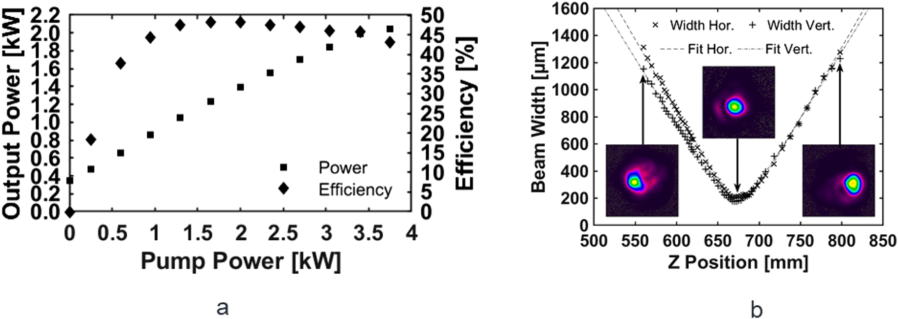
(a) Power and extraction efficiency at the exit of the second thin-disk multipass amplifier and (b) caustic in the horizontal and vertical planes and selected intensity profiles of the amplified beam at 2050 W of output power.
The beam quality factor M 2 of the beam exiting the second amplifier stage was measured to be 1.57 and 1.36 in the horizontal and vertical plane, respectively. The measured beam caustic is shown in Figure 6b. Using an auto-correlator the pulse duration at the maximum output power was measured to be 7.7 ps (FWHM) leading to a peak power of approx. 815 MW.
3.2 Amplification of femtosecond pulses
A modified Tangor HP laser from the company Amplitude was used as a seed laser for the experiments presented in [16] and in the following. It delivers up to 127 W of average output power in the first diffraction order of the internal acousto-optic modulator (AOM) at a pulse repetition rate ranging from 40 MHz down to 500 kHz. The beam propagation factor M 2 amounts to 1.25 and the pulse duration was measured to be 475 fs (FWHM). The Tangor allowed for an operation in burst mode.
To allow pulse on demand and fast modulation of the pulse train on the workpiece, polarization multiplexing was implemented (see Figure 7) by using both beams emitted from the 0th and first diffraction order of the internal AOM as seed beams. The half-wave plate introduced in the beam path of the 0th order beam allowed the rotation of its polarization by 90° with respect to that of the beam from the first diffraction order. Both beams are then recombined and injected collinearly into the TDMPA using a TFP. Beam shaping optics (spherical mirrors) are used to adapt the properties (beam diameter and divergence) of the seed beams (0th and first orders) to the diameter of the pump spot on the amplifying disk. An Yb:YAG thin-disk crystal with a doping concentration of 10–11% and a thickness of approx. 120–130 µm was used for the present experiment. The disk with a diameter of 17 mm was glued on a diamond heat sink and mounted inside a pumping unit allowing up to 24 passes of the pump radiation through the disk. Zero-phonon pumping of the Yb:YAG disk at 969 nm was implemented using a 2 kW spectrally stabilized (with a volume Bragg grating) laser diode. The radius of curvature of the disk was set to 20 m by design (see Section 2). The seed beam was geometrically folded 40 times over the Yb:YAG laser disk by means of an array of 80 adjustable mirrors. A TFP placed at the exit of the TDMPA allowed the separation of the beams originating from the 0th and first diffraction order of the seed laser. The beam from the 0th order is directed to a beam dump whereas the beam from the first order is directed to the workpiece and used for processing. The motivation to feed both beams through the amplifier is to ensure constant amplification properties by avoiding any impact on the gain when modulating the pulse sequences used for materials processing.
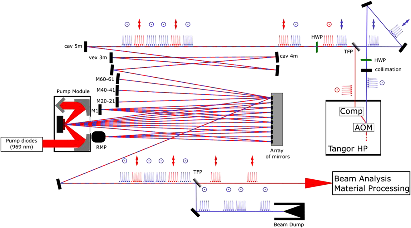
Setup of the TDMPA delivering sub-ps pulses at an average power of >1 kW and enabling modulation of the pulse train. The blue and red colors indicate the paths of the beams emitted from the 0th and the first diffraction port of the seed laser. AOM, acousto-optic modulator; Comp, pulse compressor; HWP, half-wave plate; TFP, thin-film polarizer; RMP, retro-reflecting mirror pair.
The measured output power and extraction efficiency of this laser and amplifier system are given in Figure 8a. An output power of 1058 W was achieved with an optical efficiency (seed power being subtracted) of 46%, thus corresponding to an energy per pulse of 2 mJ at a repetition rate of 500 kHz. The measured beam caustic is shown in Figure 8b. The beam propagation factor M 2 was measured to be 1.48 and 1.33 in the horizontal and the vertical plane, respectively. The pulse duration was measured to be 825 fs, thus corresponding to a peak power exceeding 2.2 GW.
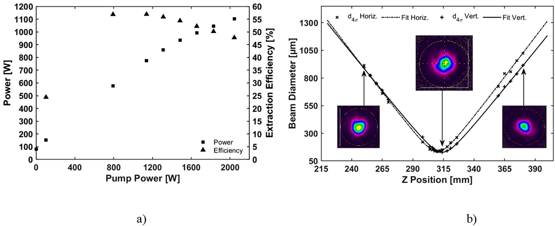
(a) Measured power and extraction efficiency of the TDMPA at a repetition rate of 500 kHz and (b) measured caustic of the emitted beam at 1059 W of average output power.
No significant difference in the extracted output power was observed when operating the system at different repetition rates or changing between single-pulse or multi-pulse burst modes. However, as shown in Figure 9, spectral broadening was observed for the single-pulse mode. This indicates the potential to compress the pulses down to a pulse duration of <100 fs. Further exploitation of this effect will be the subject of future investigations.
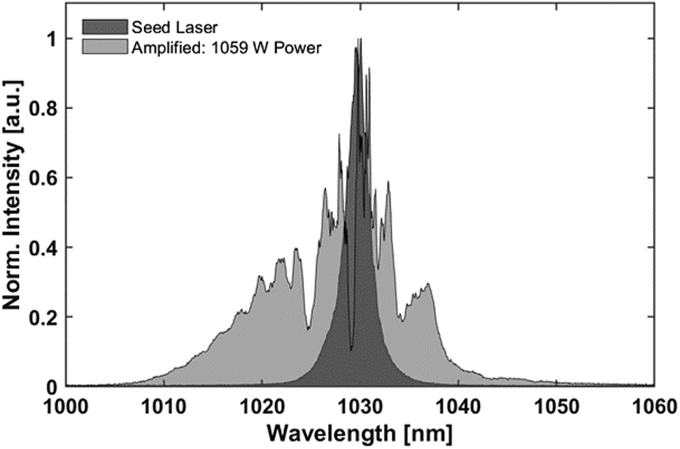
Measured spectra of the seed and the amplified beam.
To be able to use the developed laser system for material processing, its power and beam pointing stability were important criteria and were given particular attention during the development and implementation of the laser system. An excellent performance was achieved thanks to advanced designs of the optomechanical components used in the TDMPA. Temperature-controlled aluminum cast breadboards together with highly stable mirror holders and a water-cooled mirror array were custom-designed and fully qualified before their final integration. By this, a highly stable system was achieved as shown by the time-dependent power measurement illustrated in Figure 10 at a power of ∼1 kW. The measurements lasting over several hours reveal a relative standard and peak to valley deviation of 0.63 and 6%, respectively. Furthermore, the beam propagation factor M 2 was measured at the beginning and the end of the experiment. It remained unchanged over the whole measurement time. The angular beam pointing variation was measured to be <30 µrad (rms) and <100 µrad (peak to valley) in both the planes of the major and minor axes of the measured deviation ellipses.
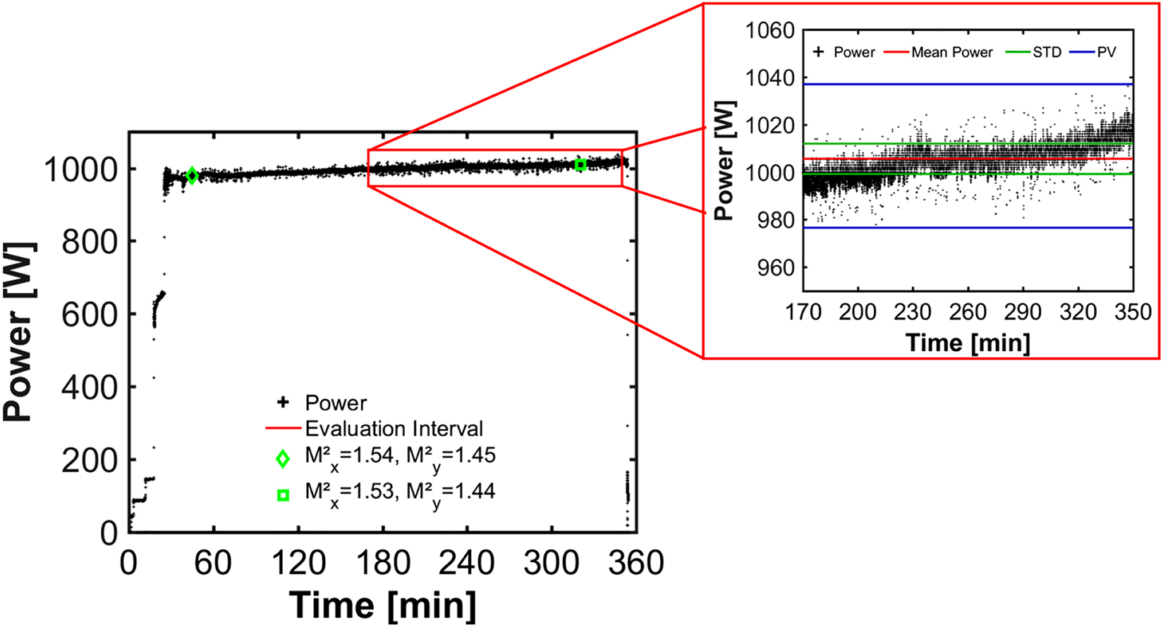
Long-term measurement of the power stability of the emitted laser beam at an average power of ∼ 1 kW.
3.3 Second and third harmonic generation
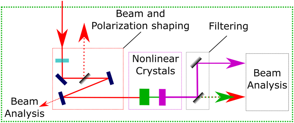
Ultrafast lasers emitting in the visible (green) and the ultraviolet spectral range offer great opportunities for many applications where the wavelength plays an important role in the light–matter interaction. The possibility to fabricate smaller structures, as well as the enhanced linear- and nonlinear absorption, can be beneficial for material processing applications such as surface structuring, drilling, micro-welding, and processing of transparent and ceramic materials [17], [18], [19], [20]. The present section is therefore devoted to our latest achievements of high powers at the wavelengths of 515 and 343 nm that were obtained by second and third harmonic generation of the infrared (IR) beams emitted from the TDMPA described above. Lithium-Triborate (LBO) crystals were used for this purpose. The obtained results are summarized in Table 1 [12], [13], [14], [15], [16]. The THG setup is depicted in Figure 11. For the SHG the second nonlinear crystal was removed and the filtering optics was adapted to separate the IR from the green beam. Furthermore, the beam shaping optics was also adapted for optimum SHG conversion.
Summary of SHG and THG experimental results obtained using the IR beam generated by our TDMPA operated in ps and fs regimes. The specifications of the LBO crystals used for the different experiments are also given in the present table.
| Pulse duration (ps) | Power (W) | Energy (mJ) | Conversion efficiency (%) | Beam quality factor (M 2) | Aperture (mm × mm) | Length (mm) | Phase matching (type: polarizations) | Crystal cut (θ, φ) | |
|---|---|---|---|---|---|---|---|---|---|
| Green (515 nm) | 0.80 | 370 | 0.740 | 47.3 | 1.40 | 10 × 10 | 1 | I: oo-e | 90°,12.9° |
| 0.60 | 440 | 0.220 | 56.1 | 1.25 | 10 × 10 | 1.5 | I: oo-e | 90°,13.6° | |
| 0.31 | 282 | 0.220 | 54.7 | 1.40 | 10 × 10 | 1 | I: oo-e | 90°,12.9° | |
| 7.7 | 1460 | 4.866 | 71.2 | 1.41 | 15 × 15 | 5 | I: oo-e | 90°,12.9° | |
| UV (343 nm) | 0.60 | 100 | 0.050 | 18.0 | 1.53 | 10 × 10 | 1 | I: oo-e | 90°,40.1° |
| 6.8 | 98 | 0.327 | 25.6 | 1.14 | 10 × 10 | 4.25 | I: oo-e | 90°,40.1° | |
| 6.8 | 137 | 0.457 | 28.5 | 1.30 | 10 × 10 | 4.25 | I: oo-e | 90°,40.1° | |
| 6.8 | 264 | 0.880 | 32 | ∼3.0 | 10 × 10 | 4.25 | I: oo-e | 90°,40.1° |
Schematic of the THG setup.
4 Material processing with >1 kW ultra-short pulses
The benefits of high average powers to increase the productivity in materials processing were demonstrated with the high-rate ablation of silicon, metals and PCD using the 1 kW sub-picosecond laser described in Section 3.2. This latter was optimized to deliver more than 1.1 kW (at a repetition rate of 500 kHz) in order to compensate for the transmission losses through the beam guiding and processing optics of the machine which were measured to be ∼9%, thus ensuring 1.01 kW of power and 2.02 mJ of pulse energy on the workpiece. The beam quality factor of the linearly polarized beam emitted from the TDMPA was remeasured to be <1.5. The beam was guided to a processing machine LS 5-1 provided by Lasea. The focusing optic (Scanlab, varioSCANde 40i) with a focal length of 580 mm was mounted to the galvanometer scanner (Scanlab, intelliSCANde 30) used for beam deflection. The maximum available feed rate was 24 m/s, limited by the dynamics of the galvanometer scanner [21].
4.1 High-quality and high-throughput laser milling of silicon and metals
Burst operation was used for the experiments presented in the following. The energy of the burst was evenly divided over five pulses within the burst (5 PPB). The pulses within the burst were separated by 22.7 ns. The focal diameter on the workpiece was measured [22] to be 90 ± 5 µm.
The benefit of processing silicon with bursts [23] was confirmed in a first experiment conducted with five pulses per burst at a low average power of 57 W and an energy per burst of 114 µJ, corresponding to a peak fluence of 0.7 J/cm2. The beam was moved over the sample’s surface with a scanning speed of 10 m/s, which corresponds to a pulse overlap of 78%. The line hatching distance was set to 20 µm. In a further experiment, 950 W (corresponding to an energy per burst of 1900 µJ) was used on the workpiece. In order to maintain a low peak fluence of 0.7 J/cm2, the beam diameter on the surface of the sample was set at 372 µm by shifting the focus position to 17 mm below the sample surface. Furthermore, the scanning speed was increased from 10 m/s to 24 m/s to maintain a moderate pulse overlap of 87% and avoid excessive melt and crack formation [24]. The corresponding surface structures as measured by scanning electron microscopy (SEM) for moderate and high average power are shown in Figure 12a and b), respectively.
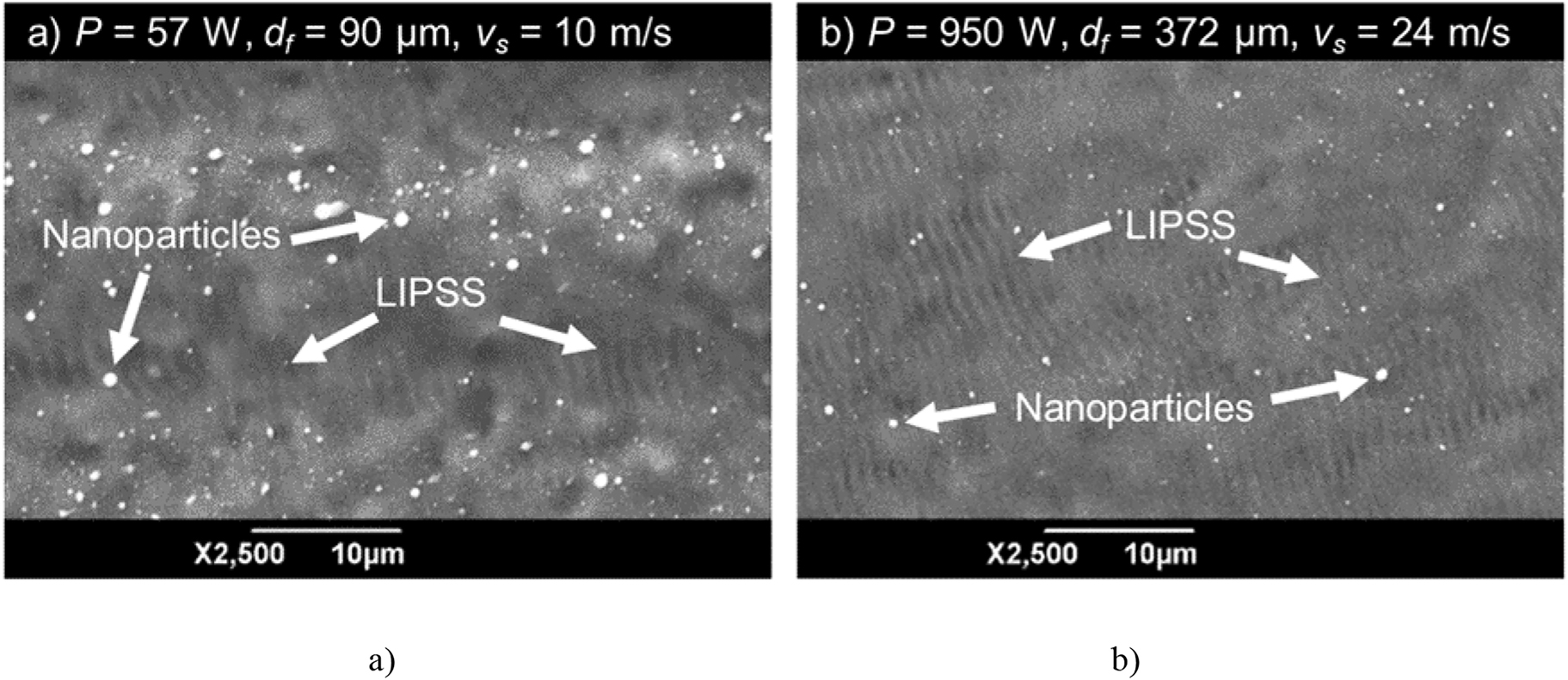
SEM images of the laser-milled surface at (a) moderate average power of 57 W and (b) high average power of 950 W d f = beam diameter n the workpiece, v s = scanning speed.
As shown from the SEM analysis of the samples obtained in both experiments, a similar surface quality covered with nanoparticles and LIPSS is obtained. The measured roughness S a is low for moderate and high average power with 0.5 and 0.4 µm, respectively. With the increased average power of 950 W, a significantly higher material removal rate of 216 mm³/min was achieved when compared to the 11 mm³/min obtained at an average power of 57 W.
The high-throughput processing was demonstrated, at an even higher power of 1010 W by milling of chamfer geometry on the workpiece corresponding to a peak fluence of 0.74 J/cm2. Figure 13 shows the topography of the processed sample as measured with a laser scanning microscope (LSM, Olympus, OLS4000). The measurement reveals a low roughness value of S a = 0.4 µm in the upper zone of the chamfered sample (region I) and S a = 0.6 µm in the lower zone (region II).
![Figure 13:
LSM measurement of a chamfer milled into a silicon wafer. Process parameters: laser wavelength = 1030 nm, power = 1010 W, inter-burst repetition rate = 500 kHz, energy per burst = 2020 µJ, number of pulses per burst = 5, peak fluence = 0.74 J/cm2 [21].](/document/doi/10.1515/aot-2021-0047/asset/graphic/j_aot-2021-0047_fig_013.jpg)
LSM measurement of a chamfer milled into a silicon wafer. Process parameters: laser wavelength = 1030 nm, power = 1010 W, inter-burst repetition rate = 500 kHz, energy per burst = 2020 µJ, number of pulses per burst = 5, peak fluence = 0.74 J/cm2 [21].
The flatness of the tilted surface was investigated by evaluating the peak-to-valley height after filtering the LSM measurement with a cut-off wavelength of 250 µm. The tilted surface is smooth with a low peak-to-valley height of 5.7 µm over the large area of 3.5 × 3.5 mm2. Although the ablated depth per scan is about 3 µm, no steps were detected along the offset parallel processed lines. The energy-specific ablated volume of 3.8 µm3/µJ during laser milling with the maximum power of 1010 W corresponds to a high material removal rate of 230 mm3/min. To the best of our knowledge, this is the highest material removal rate reported so far for laser milling of silicon with ultrafast lasers, while at the same time achieving high surface quality with S a ≤ 0.6 µm and no surface defects with diameters exceeding 1 µm. In comparison to previously reported results for laser milling of silicon achieving low surface roughness, this is 740 times higher removal rate than that reported in ref. [24] and a 443 times higher material removal rate than that reported in ref. [25]. By this one can conclude that with the combination of high average power and sub-ps pulses with an appropriate process strategy (burst mode, low peak fluence, high feed rate, etc. …) one can achieve a significant increase in laser milling throughput of silicon while maintaining high surface quality.
The potential of high throughput and simultaneously high quality in milling with 1 kW ultrafast lasers is not limited to silicon with the developed processing strategy described above. Application on widely used metals such as stainless steel, copper, and aluminum (see Figure 14) was conducted and showed comparable results to silicon with a fine ripple structure on the surface and roughness S a in the range of 1 μm at record-breaking removal rates of 126, 174 and 180 mm³/min for copper, aluminum, and stainless steel, respectively.
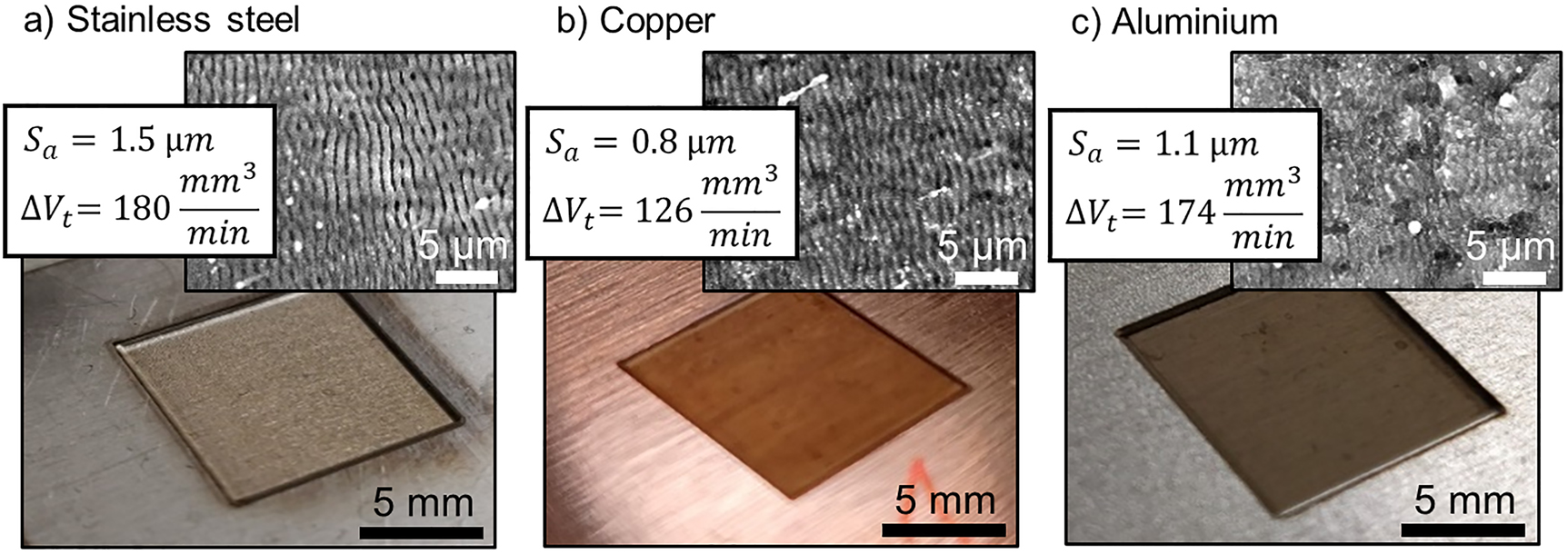
High quality and high throughputs laser milling of (a) stainless steel, (b) copper, and (c) aluminum using ultrashort laser pulses and 1.01 kW of average power.
Additionally, micrometer size ripple structures were generated on the surface by the laser milling process. These ripples allow for potential applications to adjust the structural color, the wetting behavior, cell growth, or friction behavior of the processed surface [19]
4.2 High quality and high throughput laser milling of diamond
The same laser and processing machine (described in Section 4.1) were also used for the ablation of PCD. The usable power on the workpiece was slightly lower (990 W instead of 1010 W) due to a slight misalignment of the TDMPA. These investigations are reported in detail in ref. [26]. Bursts containing three pulses were used for the experiments which showed an increase of the ablation rate by a factor of 140 as compared to traditional mechanical processes and by up to 70 times when compared to the use of state of art 100 W-class fs lasers. A 14% reduction of the initial surface roughness S a was also achieved by using the 3-pulses burst and can be further improved by the use of higher numbers of pulses per burst (>5). Last but not least no phase transformation, as revealed by Raman spectroscopy analysis of the processed samples, was observed when processing at ∼1 kW of average power [26].
5 Conclusions
An overview of the latest achievements in the development of high-power (>1 kW) thin-disk multipass amplifiers including second and third harmonic generation is given in the present paper. The scaling of the productivity was demonstrated with high-throughput materials processing using average laser powers in the order of 1 kW and sub-ps pulses for laser milling of silicon, metals, and PCD. Future development will be dedicated to the development of laser systems providing a higher level of flexibility in terms of pulse duration (e.g. from ms to fs), pulse repetition rate (e.g. from kHz to GHz), adjustable burst shapes as well as the development of beam shaping optics for ultra-short pulses at average powers of >1 kW.
Funding source: European Union’s Horizon 2020 Research and Innovation Programme
Award Identifier / Grant number: 687613 & 687880
Acknowledgment
EU H2020 Projects Hiperdias (www.hiperdias.eu), Tresclean (www.tresclean.eu). The presented results are done within PhD work of, Daniel Holder, André Loescher, Christoph Roecker, and William Scalbert.
-
Author contributions: All the authors have accepted responsibility for the entire content of this submitted manuscript and approved submission.
-
Research funding: This work was funded by the European Union’s Horizon 2020 Research and Innovation Programme under Grant Agreement No. 687613 & 687880.
-
Conflict of interest statement: The authors declare no conflicts of interest regarding this article.
References
[1] F. Saltarelli, I. J. Graumann, L. Lang, D. Bauer, C. R. Phillips, and U. Keller, “350-W average-power SESAM-modelocked ultrafast thin-disk laser,” in Conference on Lasers and Electro-Optics Europe and European Quantum Electronics Conference 2019, OSA Technical Digest (Optical Society of America), 2019. paper cf_1_1.10.1109/CLEOE-EQEC.2019.8873033Search in Google Scholar
[2] C. J. Saraceno, F. Emaury, O. H. Heckl, C. R. E. Baer, M. Hoffmann, C. Schriber, M. Golling, T. Südmeyer, and U. Keller, “275 W average output power from a femtosecond thin disk oscillator operated in a vacuum environment,” Opt. Express, vol. 20, pp. 23535–23541, 2012, https://doi.org/10.1364/OE.20.023535.Search in Google Scholar PubMed
[3] C. J. Saraceno, F. Emaury, C. Schriber, M. Hoffmann, M. Golling, T. Südmeyer, and U. Keller, “Ultrafast thin-disk laser with 80 μJ pulse energy and 242 W of average power,” Opt. Lett., vol. 39, pp. 9–12, 2014, https://doi.org/10.1364/OL.39.000009.Search in Google Scholar PubMed
[4] J. Brons, V. Pervak, D. Bauer, D. Sutter, O. Pronin, and F. Krausz, “Powerful 100-fs-scale Kerr-lens mode-locked thin-disk oscillator,” Opt. Lett., vol. 41, pp. 3567–3570, 2016, https://doi.org/10.1364/OL.41.003567.Search in Google Scholar PubMed
[5] H. Stark, J. Buldt, M. Müller, A. Klenke, and J. Limpert, “1 kW, 10 mJ, 120 fs coherently combined fiber CPA laser system,” Opt. Lett., vol. 46, pp. 969–972, 2021, https://doi.org/10.1364/OL.417032.Search in Google Scholar PubMed
[6] M. Müller, C. Aleshire, A. Klenke, E. Haddad, F. Légaré, A. Tünnermann, and J. Limpert, “10.4 kW coherently combined ultrafast fiber laser,” Opt. Lett., vol. 45, pp. 3083–3086, 2020, https://doi.org/10.1364/OL.392843.Search in Google Scholar PubMed
[7] A. Giesen, H. Hügel, A. Voss, K. Wittig, U. Brauch, and H. Opower, “Scalable concept for diode-pumped high-power solid-state lasers,” Appl. Phys. B, vol. 58, pp. 365–372, 1994, https://doi.org/10.1007/BF01081875.Search in Google Scholar
[8] A. Killi, C. Stolzenburg, I. Zawischa, D. Sutter, J. Kleinbauer, S. Schad, R. Brockmann, S. Weiler, J. Neuhaus, S. Kalfhues, E. Mehner, D. Bauer, H. Schlueter, and C. Schmitz, “The broad applicability of the disk laser principle - from CW to ps,” Proc. SPIE-Int. Soc. Opt. Eng., vol. 71931T, p. 71939, 2009, https://doi.org/10.1117/12.808255.Search in Google Scholar
[9] T. Nubbemeyer, M. Kaumanns, M. Ueffing, M. Gorjan, A. Alismail, H. Fattahi, J. Brons, O. Pronin, H. G. Barros, Z. Major, T. Metzger, D. Sutter, and F. Krausz, “1 kW, 200 mJ picosecond thin-disk laser system,” Opt. Lett., vol. 42, pp. 1381–1384, 2017, https://doi.org/10.1364/OL.42.001381.Search in Google Scholar PubMed
[10] J.-P. Negel, A. Voss, M. Abdou Ahmed, D. Bauer, D. Sutter, A. Killi, and T. Graf, “1.1 kW average output power from a thin-disk multipass amplifier for ultrashort laser pulses,” Opt. Lett., vol. 38, pp. 5442–5445, 2013, https://doi.org/10.1364/OL.38.005442.Search in Google Scholar PubMed
[11] M. Abdou Ahmed, C. Roecker, A. Loescher, et al.., “Development of high-power ultrafast lasers: quo Vadis?,” Proc. SPIE, vol. 11664, 2021. https://doi.org/10.1117/12.2593113.Search in Google Scholar
[12] J.-P. Negel, A. Loescher, A. Voss, D. Bauer, D. Sutter, A. Killi, M. Abdou Ahmed, and T. Graf, “Ultrafast thin-disk multipass laser amplifier delivering 1.4 kW (4.7 mJ, 1030 nm) average power converted to 820 W at 515 nm and 234 W at 343 nm,” Opt. Express, vol. 23, pp. 21064–21077, 2015, https://doi.org/10.1364/OE.23.021064.Search in Google Scholar PubMed
[13] Hiperdias Project, Funded from the European Union’s Horizon 2020 Research and Innovation Programme under Grant Agreement No. 687880, Available at: https://cordis.europa.eu/project/id/687880.Search in Google Scholar
[14] Tresclean Project, Funded from the European Union’s Horizon 2020 Research and Innovation Programme under Grant Agreement No. 687613. Available at: www.tresclean.eu (accessed: Sept. 21, 2021).Search in Google Scholar
[15] Flexiburst Project, Funded from the European Union’s Horizon 2020 Research and Innovation Programme under Grant Agreement No 825246. Available at: www.kW-flexiburst.eu (accessed: Sept. 21, 2021).Search in Google Scholar
[16] C. Röcker, A. Loescher, F. Bienert, P. Villeval, D. Lupinski, D. Bauer, A. Killi, T. Graf, and M. Abdou Ahmed, “Ultrafast green thin-disk laser exceeding 1.4 kW of average power,” Opt. Lett., vol. 45, pp. 5522–5525, 2020, https://doi.org/10.1364/OL.403781.Search in Google Scholar PubMed
17 C. Röcker, A. Loescher, M. Delaigue, C. Hönninger, E. Mottay, T. Graf, and M. A. Ahmed, “Flexible sub-1 ps ultrafast laser exceeding 1 kW of output power for high-throughput surface structuring,” in Laser Congress 2019 (ASSL, LAC, LS&C), Optical Society of America, 2019, p. AM4A.2.10.1364/ASSL.2019.AM4A.2Search in Google Scholar
[18] A. Feuer, C. Kunz, M. Kraus, V. Onuseit, R. Weber, T. Graf, D. Ingildeev, and F. Hermanutz, “Influence of laser parameters on quality of microholes and process efficiency,” in Proc. SPIE 8967, Laser Applications in Microelectronic and Optoelectronic Manufacturing (LAMOM) XIX, 2014, p. 89670H.10.1117/12.2037674Search in Google Scholar
[19] J. Bonse, S. Höhm, S. V. Kirner, A. Rosenfeld, and J. Krüger, “Laser-Induced periodic surface structures— a scientific evergreen,” IEEE J. Sel. Top. Quant. Electron., vol. 23, no. 3, 2017, Art no. 9000615, https://doi.org/10.1109/JSTQE.2016.2614183.Search in Google Scholar
20 S. Richter, M. Heinrich, S. Döring, A. Tünnermann, and S. Nolte, “Formation process of femtosecond laser-induced nanogratings at high repetition rates,” in CLEO/Europe and EQEC 2011 Conference Digest, OSA Technical Digest (CD), Optical Society of America, 2011. paper CM1_5.10.1109/CLEOE.2011.5943317Search in Google Scholar
[21] K. Cvecek, S. Dehme, I. Miyamoto, and M. Schmidt, “A review on glass welding by ultra-short laser pulses,” Int. J. Extrem. Manuf., vol. 1, no. 4, 2019, https://doi.org/10.1088/2631-7990/ab55f6.Search in Google Scholar
[22] J. M. Liu, “Simple technique for measurements of pulsed Gaussian-beam spot sizes,” Opt. Lett., vol. 7, pp. 196–198, 1982, https://doi.org/10.1364/OL.7.000196.Search in Google Scholar
[23] B. Neuenschwander, B. Jaeggi, D. J. Foerster, T. Kramer, and S. Remund, “Influence of the burst mode onto the specific removal rate for metals and semiconductors,” J. Laser Appl., vol. 31, no. 2, 2019, Art no. 022203. https://doi.org/10.2351/1.5096083.Search in Google Scholar
[24] D. Holder, R. Weber, C. Röcker, G. Kunz, D. Bruneel, M. Delaigue, T. Graf, and M. Abdou Ahmed, “High-quality high-throughput silicon laser milling using a 1 kW sub-picosecond laser,” Opt. Lett., vol. 46, pp. 384–387, 2021, https://doi.org/10.1364/OL.411412.Search in Google Scholar PubMed
[25] D. Metzner, P. Lickschat, and S. Weißmantel, “Investigations of qualitative aspects with burst mode ablation of silicon and cemented tungsten carbide,” Appl. Phys. A, vol. 125, p. 411, 2019, https://doi.org/10.1007/s00339-019-2696-4.Search in Google Scholar
[26] W. Scalbert, D. Tanner, M. Delaigue, C. Hönninger, D. Brunel, D. Holder, C. Röcker, and M. Abdou Ahmed, “Development of high-power laser ablation process for polycrystalline diamond polishing: part 3. processing with an ultra-short-pulsed laser up to 1kW,” in Proc. SPIE 11679, High-Power Laser Materials Processing: Applications, Diagnostics, and Systems X, 2021, p. 116790H.10.1117/12.2579250Search in Google Scholar
© 2021 Marwan Abdou Ahmed et al., published by De Gruyter, Berlin/Boston
This work is licensed under the Creative Commons Attribution 4.0 International License.
Articles in the same Issue
- Frontmatter
- Topical Issue: High-rate Laser Processing; Guest Editors: Jörg Schille and Udo Löschner
- Editorial
- Ultrashort pulse lasers in high-rate laser micro processing – Quo vadis?
- Views
- The challenges of productive materials processing with ultrafast lasers
- Review Articles
- High-power modelocked thin-disk oscillators as potential technology for high-rate material processing
- GHz femtosecond processing with agile high-power laser
- Research Articles
- High-power ultrafast fiber lasers for materials processing
- High-power ultrafast thin-disk multipass amplifiers for efficient laser-based manufacturing
- Accelerating laser processes with a smart two-dimensional polygon mirror scanner for ultra-fast beam deflection
- Pulse-on-demand laser operation from nanosecond to femtosecond pulses and its application for high-speed processing
- Multi beam microprocessing for printing and embossing applications with high power ultrashort pulsed lasers
- High-rate laser processing with ultrashort laser pulses by combination of diffractive elements with synchronized galvo scanning