
Multi-scale alignment to buried atom-scale devices using Kelvin probe force microscopy
-
Pradeep Namboodiri
 ,
Jonathan Wyrick
,
Jonathan Wyrick

Abstract
Fabrication of quantum devices by atomic-scale patterning with scanning tunneling microscopy (STM) has led to the development of single/few atom transistors, few-donor/quantum dot devices for spin manipulation, and arrayed few-donor devices for analog quantum simulation. We have developed atomic precision lithography, dopant incorporation, device encapsulation, ex situ device re-location, and contact processes to enable high-yield device fabrication. In this work, we describe a multiscale alignment strategy using Kelvin probe force microscopy to enable the alignment of buried device components to electronic support structures such as source/drain leads, in-plane and top gates, and waveguides while preserving flexibility in the placement of fabricated STM patterns. The required spatial accuracy to bridge the sub-micrometer scale central region of the device to millimeter scale large wire-bond pads is achieved through a multi-step alignment process at various stages of fabrication, including atom-scale device fabrication using STM, re-location and registration, and electron beam lithography for contact leads and pads. This alignment strategy allows imaging small device regions as well as large-scale fiducial marks, thereby bridging the gap from nanometer STM patterns to the millimeter-scale electrical contact fabrication with a 95% yield on more than 150 devices fabricated to date.
Graphical abstract
1 Introduction
Scanning tunneling microscopy (STM)-based lithography on silicon surfaces has been used to fabricate devices with near single-atom positioning accuracy [1–11]. Such devices are excellent test vehicles to observe quantum phenomena at the atomic scale and further advance technological applications in the realm of quantum information science [12–16], and analog quantum simulation [17–20]. For example, it has been proposed that this method can be used to create large-scale qubit systems implementing a surface code quantum computer [21]. The core technology behind the fabrication of these devices is hydrogen depassivation lithography [22–24]. An STM tip is used to selectively desorb hydrogen atoms from a hydrogen-terminated Si (100) surface while the exposed dangling silicon bonds foster the precise placement of phosphorous dopants [25]. The atom-scale fabrication processes take place in an ultra-high vacuum (UHV) environment and the devices are encapsulated in epitaxial silicon. The result is a fully encapsulated and protected two-dimensional dopant device buried under epitaxial silicon that often leaves little to no topographic signature at the surface. A variety of such dopant-based devices have been fabricated by this method in the last decade, demonstrating a viable path for the realization of multi-qubit devices [12,13,26]. One of the key fabrication challenges for these devices is achieving sub-micron positioning accuracy of electrical contacts to the buried STM-fabricated structures [27]. The accurate alignment of contacts is a key requirement in enabling high-yield STM-based device fabrication. This also has important applications with regard to mating buried devices to other types of on-chip electronic/quantum devices such as local top gates, high-frequency lines for nuclear magnetic resonance/electron spin resonance, complementary metal-oxide-semiconductor (CMOS) structures, and microwave resonators. The methods used for fabrication in this article, hydrogen passivation, lithography, phosphine dosing, phosphorous incorporation, and silicon overgrowth, are essentially the same as those used by the Simmons group [28] with the exception of the alignment strategy described here which is the primary focus of this work.
Various methods have been proposed for the positioning and connectivity of atomic-scale STM patterns to micrometer scale contacts and leads. Methods based on having a pre-defined location of STM pattern [27–29] on the chip have advantages in terms of contact alignment, but on the other hand, this imposed patterning location might not have the best surface quality for device fabrication. Ruess et al. [28] demonstrated a method to pattern a device aligned to a pre-etched registration mark allowing direct patterning of contacts using electron-beam lithography (EBL) since the device is already registered during fabrication. However, this method limits the flexibility in the choice of device location and requires performing large area survey scans to locate registration marks. Another approach is to use pre-deposited metal marks [29] or pre-implanted contacts [30], which has the advantage that once the device has been patterned, the sub-micron to millimeter-scale contact is already formed and may prove useful to fabricate devices that can be operated in situ STM. This approach, however, restricts the standard high-temperature treatments required to obtain pristine silicon surfaces and similarly suffers from the requirement for large survey scans before patterning. It is likely that high yield and reproducible atomic-precision fabrication using STM demands the selection of surface regions that are clean and have a minimum of defects. Once such a high-quality surface region is selected and the STM patterns defined, we need to be able to re-locate these patterns and align the contacts to them. In addition, the patterned STM devices and pad sizes are kept to only a few micrometers in size because of the time constraint associated with exposure of the device layer to potential contamination. It is therefore necessary to have a precise and robust alignment strategy for making electrical contacts to relatively small STM pads that have little if any variation in post-encapsulation topography compared to their surroundings. Since devices are located relatively close to the surface (∼30 nm below), it is also necessary to utilize non-invasive post-fabrication processes to preserve the device quality during re-location. Here, we define “re-location” to mean determination of the location of an encapsulated device after it has been removed from UHV. It should be noted that the re-location adds one day to the overall process. This replaces a required initial in situ step of performing large area survey scans and positioning the STM tip with respect to the pre-etched fiducial marks which itself can take several hours. The overall process for making a single fully functional device from in situ STM patterning to aligned contact fabrication takes roughly 2 weeks.
There are a few options in the imaging techniques used to re-locate the STM fabricated patterns, each of them with its own advantages and disadvantages. Based on its differential conductance contrast, the STM itself is sensitive enough to image shallow subsurface doped regions like the ones in phosphine-doped silicon devices [15,19]. However, the limited vertical and lateral operational range of the STM makes it difficult to measure the taller microscale etched fiducial marks that are used for device registration. Second, common atomic force microscopy (AFM) topographical modes like contact or tapping modes might be used to locate surface features within the necessary nanometer-to-micrometer scanning range, but they have no contrast for buried devices that show little to no topographic perturbations on the top surface. Finally, some specialized AFM modes like scanning capacitance microscopy and scanning microwave microscopy featuring long-range electronic contrast have proven capable of imaging buried patterned dopant devices within scans comprising micrometer-scale areas [29,31,32]. Both techniques produce high-contrast images of buried devices, but they operate in contact mode while applying voltage across the tip-sample contact and have the potential of causing surface oxidation and modification of the silicon surface [33].
To address most of the issues discussed above, we employed a minimally invasive scanning probe technique, namely Kelvin probe force microscopy (KPFM) [34,35], to re-locate and register patterned STM devices with respect to a pre-etched 50 µm grid of reference fiducial marks. With KPFM operating in a dual-pass mode, it is possible to scan relatively large areas encompassing the fabricated devices and have both the surface topography from a mechanical intermittent contact mode like tapping or PeakForce tapping performed in the first pass of the scan and the surface potential map from an electrical modulation carried out in the second pass at 50–70 nm lift height above the scanned surface. The topography and the potential map are commensurate to one another and hence can be overlaid using a semi-automated algorithm to identify the location of the device with respect to the nearest fiducial marks. In the last several years, we successfully developed a precise and accurate method to fabricate and align STM-patterned quantum devices [3,04,17], and here, we present in detail the alignment methodology behind this process.
2 Methods
2.1 Device fabrication
The alignment method presented in this work spans over all device fabrication stages, including the re-location done by KPFM. First, we start with silicon chips that have a coordinate system defined by two sets of fiducial marks that are pre-etched on each chip (Figure 1a and b). These two sets of pre-etched patterns consist of: (1) STM-compatible fiducial marks that are an array of 50 μm × 50 μm features over the central region of the chip within which any STM-patterned device will be located and (2) EBL alignment marks that are an array including chip alignment marks near the peripheral parts of the chip for high precision alignment of EBL. Both sets of fiducial marks are fabricated by optical lithography with an ASML Stepper PAS 5500/275D[1] (ASML, Veldhoven, The Netherlands) having a specified overlay accuracy of 40 nm across the wafer. The wafers that we use are boron-doped float zone silicon wafers with a resistivity of 1–10 Ω cm manufactured by Virginia Semiconductors (see footnote 1). The STM fiducial marks are etched to nominally 100 nm deep and the EBL alignment marks are nominally 2 µm deep. This allows scanning probe imaging of the fiducials near devices without damaging the probe tip and provides a means to determine scan locations relative to the EBL alignment marks. Second, the pre-etched chips are loaded into a UHV-STM system, flash annealed at 1,200°C to obtain a clean silicon (100) surface, and then hydrogen passivated. We have previously observed and used the presence of these pre-etched features to help modify the step-terrace features leaving relatively large terraces [36]. Third, STM patterning of a device is then carried out at a location with few defects within one of the pre-etched squares. This is followed by phosphorous deposition and incorporation, and then epitaxial silicon is overgrown at 250°C [37] to activate and encapsulate the device. To optimize and baseline the fabrication process, the presence and the vertical confinement of the phosphorous δ-layer fabricated by this process is confirmed by other techniques [38]. Figure 1d shows the image of an STM patterned device, a single electron transistor (SET) during hydrogen lithography prior to phosphorus dosing and silicon encapsulation. The featured SET island tunnel couples to two leads serving as source (S) and drain (D), respectively, and two gates (Gate 1 and Gate 2), so the electron occupancy of the quantum dot can be controlled through the capacitive coupling between the gates and the doped island. These electrodes extend to contact pads from which larger electrical leads for outside connectivity are further defined by subsequent EBL patterning and metallization (Figure 1e and f). To have a precise alignment of the contacts over the STM patterned device pads, the location of this active area must be registered first within the reference coordinate system of the STM fiducial marks (Figure 1b), and, in our method, this registration is provided by KPFM scans over the region of interest.
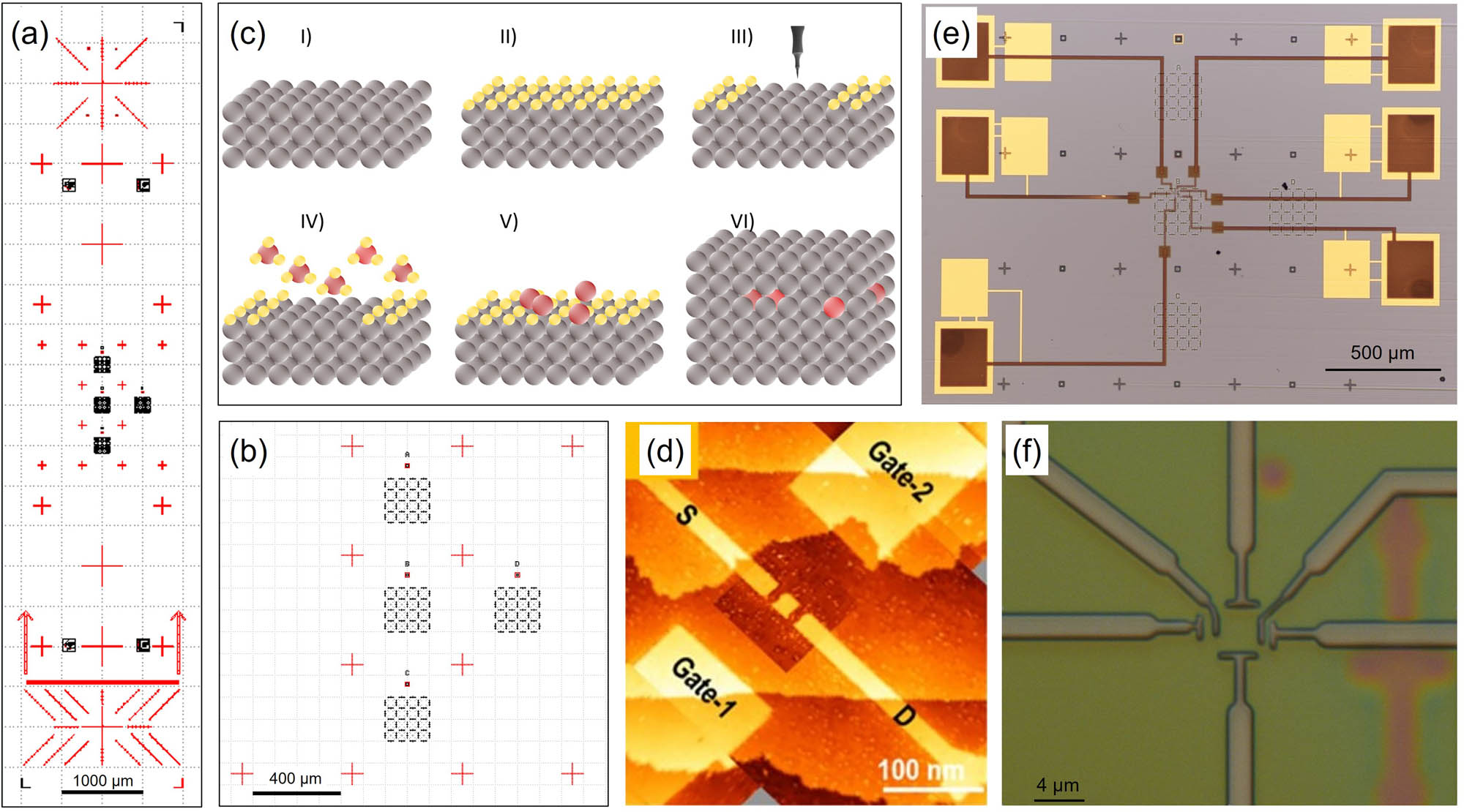
(a) Layout of registration marks on a chip showing the two sets of pre-patterned fiducial marks, namely the STM fiducial marks (the four black arrays of squares in the middle of the chip) and the global and local alignment marks for EBL (red marks). (b) Enlarged view of the array of squares used as STM fiducial marks on the center of the chip. (c) The main steps of hydrogen depassivation lithography for device fabrication: (I) clean silicon surface, (II) hydrogen passivation, (III) tip-induced lithography to selectively remove hydrogen atoms, phosphine (IV) dosing and (V) incorporation, and (VI) intrinsic silicon overgrowth. (d) STM images of a quantum dot connected to source and drain as well as two gate electrodes. (e) Large-scale optical image showing a finished chip with electrical leads from the device electrodes extending to bond pads. (f) Optical image of metal contacts over an encapsulated device.
2.2 KPFM
The KPFM that we used was in the form of PeakForce™ frequency-modulation KPFM (PeakForce FM-KPFM) (Multimode AFM, Bruker [see footnote 1] Santa Barbara), which is an AFM dual scanning mode with a topography scan acquired first in PeakForce tapping mode followed by a second scan line with KPFM data acquired at a given tip height above the surface [35]. The use of the PeakForce FM-KPFM scanning mode provides three main advantages: (1) reduced mechanical damage [39] of the surface during the topographical scanning since the PeakForce is an intermittent contact mode operating with feedback control based on the maximum applied contact force, (2) the bias voltage applied during the KPFM scanning portion is done at a constant height (typically 50 nm) above the surface, so no oxidation damage is produced on the surface; this is in contrast to possible unintentional oxidation induced by the bias changes occurring with other AFM modes [33,40–43]; (3) the FM-KPFM variant provides an enhanced spatial resolution compared to AM-KPFM due to reduced capacitive coupling between the cantilever and the sample being imaged. The AFM tips used for these scans were Platinum-Iridium coated, electrically conductive tips (SCM PIT_V2, Bruker [see footnote 1] AFM Probes), with the first resonant frequency nominally 60 kHz and cantilever stiffness around 3 N/m. The scan rate was equal to or less than 0.5 Hz because of the large scan area involving etched fiducial marks. As such, the total time required for one single scan varied between 45 and 60 min depending on the desired pixel resolution.
3 Results and discussion
3.1 KPFM imaging for device relocation
The imaging contrast of the KPFM is due to the variation in contact potential difference (CPD),
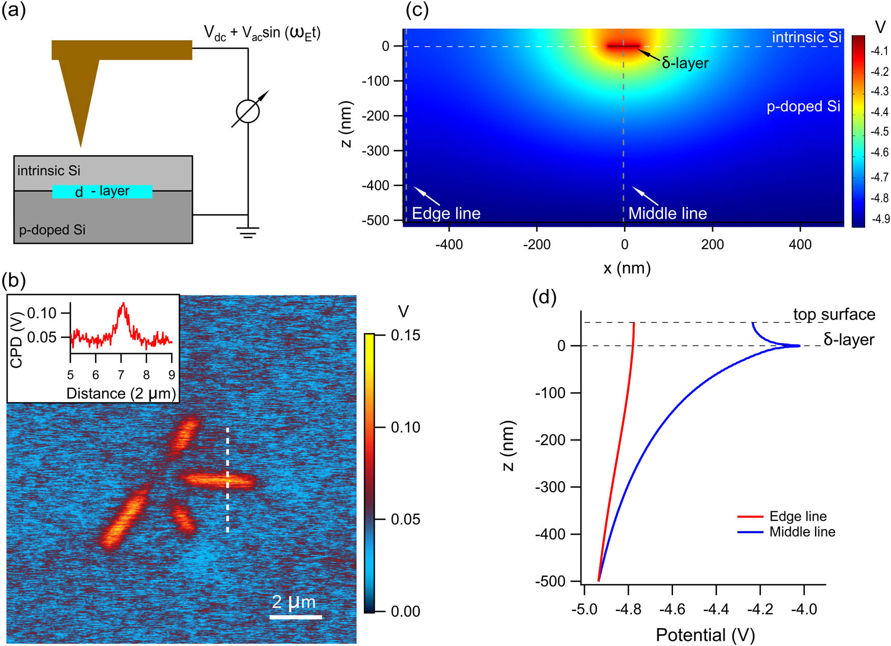
(a) KPFM setup over a Si-based heterostructure that incorporates a δ-layer (blue) between the p-doped substrate (dark gray) and the nominally intrinsic top encapsulation (light gray). (b) KPFM contrast measured over an area consisting of a phosphorous-doped device. The inset shows tip-sample CPD along the dotted line. (c) The calculated 2D electrical potential map of a Si-based heterostructure that mimics the cross-section of the actual layer structure of a doped buried device. (d) Vertical cross-sections from (c) across regions with (middle line) and without (edge line) δ-layer doping.
To illustrate the variation in the surface CPD due to a buried δ-layer we simulate the surface potential of a δ-layer region using the semiconductor module of the COMSOL Multiphysics platform (COMSOL Inc., Burlington, MA, USA [see footnote 1]). The Poisson–Boltzmann equation for the space charge distributions of carriers and ionized dopants across a 2D section of a doped heterostructure was solved. The model allows carrier movement using drift equations to satisfy the equilibration of the Fermi level across interfaces and at boundaries. The simulated subsurface electric potential across a silicon heterostructure is shown in Figure 2c, where the layer structure and electron doping profile implemented in the simulation are similar to those used in our devices, namely n = 1012 cm−3 over 30 nm (for the encapsulating top layer), n = 1020 cm−3 over 3 nm (for the highly doped δ-layer), and p = 1015 cm−3 over 500 nm (for the substrate) where n is the doping concentration. Within the classical Poisson–Boltzmann approximation for doping confinement, the simulation shows a change in the electrical potential across the subsurface region in the presence of the highly doped region below a 30 nm thick encapsulation that qualitatively reproduces the contrast seen in KPFM. A more accurate model of the surface potential introduced by the δ-layer would require taking into account: atomistic details, probe geometry, and surface conditions of the sample and the probe, such as surface dipoles, surface states, oxide layer, and humidity which are beyond the scope of this work. The presence of the δ-layer and high carrier concentration modulates the electric field resulting in band bending that extends to the surface; this effect is measurable as a local variation in surface potential above δ-doped regions when compared to undoped regions (refer to the profiles shown in Figure 2d). As explained above, KPFM is sensitive to this local change in surface potential and is used to image the buried devices.
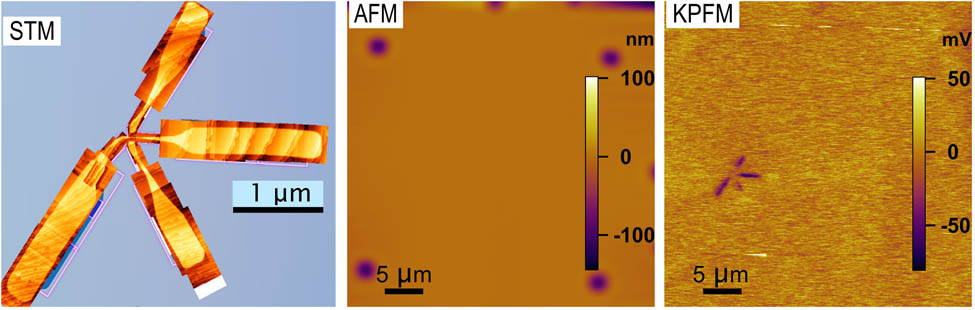
The scan region to relocate a device using KPFM mapping is chosen based on an optical image of the tip-sample reflection point captured in the UHV system, as shown in Figure 3a. The STM scan of a device with extended contact pads is shown in Figure 3b. Since KPFM has a large scan range capability, we can quickly locate buried devices. An example of a KPFM scan is shown in Figure 3c (topography) and d (surface potential) over a 40 µm × 40 µm scan area with the STM fiducial marks visible in both topography and surface potential images and the extended contact pads of the device clearly visible only in the surface potential image.

(a) Optical images acquired with a long working distance camera (two different camera angles are used to triangulate the sample position) of the STM tip and the sample; round inset is a zoom showing the STM tip and its reflection indicating an approximate location of the patterned device with respect to the STM fiducial marks. (b) STM image of a device after patterning showing device components leading to larger device pads. (c) AFM topography and (d) KPFM surface potential maps used to locate the device from (b) within four nearby STM fiducial marks.
3.2 Overlay and alignment procedure
From KPFM images the relative position of an STM-patterned device with respect to the STM-compatible fiducial marks is extracted and then used to register the device with respect to EBL alignment marks. We have developed a multiscale alignment scheme, where images ranging from atomic-scale STM images to micrometer-scale AFM scans and optical microscopy images can be overlaid on a chip layout defined by the CAD file used to generate fiducial marks (a GDS-2 file[2]). In most cases, we find that alignment can be achieved by using a combined minimal subset of images consisting of AFM topography, KPFM map, and STM fiducial layout of the GDS-2 file. As shown in Figure 3, we acquire AFM scans large enough to include both the encapsulated device and several distinct shallow etched STM fiducial marks. Distortion is common in large scanning probe images as a result of creep, drift, and hysteresis of the piezo-electric scanner, resulting in an inaccurate device location relative to the fiducial marks. We account for these distortions by enforcing agreement of four “control” points in the AFM topography image with the four equivalent points in the GDS-2 file, as illustrated in Figure 4.
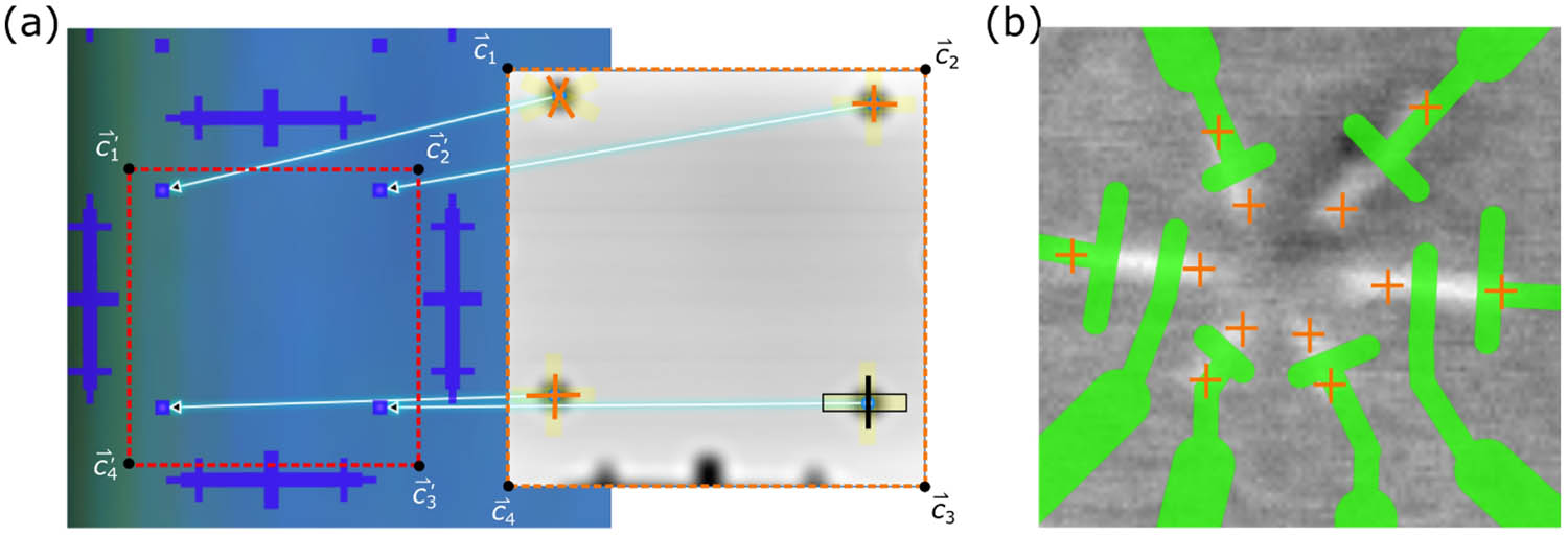
(a) Mapping an AFM topography (orange dashed outlined square in the middle of the figure) to the GDS-2 fiducial design coordinates (red dashed outlined square in the left part of the figure). The regions around the STM fiducial marks on the AFM topography (yellow rectangles) are analyzed to determine the centers of the fiducial marks (orange and black cross lines). Overlayed perpendicular (or near perpendicular) sampling regions (yellow rectangles) are chosen from the topography image to generate two center lines (orange solid lines) whose intersection defines the center of the circular etched feature; one bottom right sampling region is highlighted (black outline) and its corresponding center line is marked in black for clarity. The locations of these centers are then mapped (blue arrows) to the corresponding points on the GDS-2 file. (b) The final planned EBL contacts (green leads) are overlaid on the KPFM image (contact pads in white with ends marked by orange crosses).
Without imposing additional constraints, there is no unique mapping from four points on a given 2D image to four points on another image, particularly in the case where we know one image was generated with piezo distortion in which straight lines can become curved. As for our mapping we choose a simple linear mapping, where for a given point
and we impose a similar relationship for the transformed point,
where we assume that the coefficients
The four control points are chosen based on the available STM fiducial marks in the vicinity of the device. According to our design, the device will be found between some set of four circular STM fiducial marks that can be imaged simultaneously (see Figure 4a). Given the finite lateral width (∼100 nm) of the etched fiducials after anneal, their precise locations in the AFM topography image are not well-defined so we have adopted a semi-automated edge detection approach to determine the centers of the circular marks: as shown in Figure 4a, rectangular regions (yellow rectangles) from the AFM topography image were chosen to calculate the center lines of the STM fiducial marks (the source code of this procedure is available at reference [44].
The algorithm for determining the center lines of the STM fiducials treats them as topographic trenches having parabolic minima. A given rectangular region of the image is separated into a series of horizontal lines (i.e., horizontal “scan lines”) or profiles. A least-squares parabolic fit is then applied to each profile in a neighborhood about its absolute minimum to determine the x-coordinate of the minimum (here x is the horizontal position of the local coordinate system defined by the chosen rectangular region). Each of these x-coordinates (one per profile) is then least-squares fit with a line that represents the algorithm’s best estimate of the center line of the STM fiducial mark. Two non-parallel regions overlaid on a circular mark can be used to find the center point as the intersection of their two respective center lines (refer to the black rectangle and line for the lower-right fiducial on the AFM image of Figure 4a); this intersection acts as a well-defined control point that can be mapped to the equivalent position in the GDS-2 file.
Once the AFM topography image has been properly overlaid with the planar geometry of the GDS-2 file, the same mapping can be used to overlay the KPFM image since it is commensurate (notably the four-point mapping should be done separately for the trace (forward scan) and retrace (reverse scan) AFM images to account for the reverse scan image that might not be fully commensurate with the forward scan image. Having generated transformed images that show the locations of the STM-fabricated contact pads properly overlaid relative to fiducials, we then mark (crosses in Figure 4b) relevant positions given by the GDS-2 file to guide the alignment of the EBL contact pattern. The code developed by Wyrick [44] for STM patterning, data acquisition, and analysis with overlay utilities to accurately determine device coordinates is available for download in the Github repository for public use.
3.3 Overall uncertainty estimation
The uncertainty of the alignment method has contributions from each of the three stages of the fabrication process. The first is fabrication of etched STM fiducial marks and EBL registration marks before STM patterning. Lithography overlay for this is accomplished using an ASML Stepper PAS 5500/275D (see footnote 1) which has a specified overlay accuracy of 40 nm. The second process involves registration of the device to STM fiducials using KPFM and the mapping algorithm to overlay the images to optical and GDS-2 files. We found out that repetitive coordinate re-mapping of the STM fiducials from successive KPFM images can be used to further reduce the associated uncertainty. For a series of devices, we determined that the KPFM positioning uncertainty (1 standard deviation) was 140 nm. The third process is the EBL alignment during patterning for metallization. We routinely use a JEOL JBX 6300-FS (see footnote 1) (Jeol Ltd, Akishima, Tokyo, Japan) direct write EBL which has a specified positioning accuracy of 20 nm. By combining the standard uncertainties from the three different alignment steps mentioned above, the overall uncertainty estimate from all three levels of alignment is about 160 nm. This indicates that the overall uncertainty is dominated by the uncertainty introduced by the registration of the KPFM images to the fiducial grids. The shapes of the EBL patterned contacts (shown as green in Figure 4b) are designed to compensate for this uncertainty. This is evidenced by successful electrical measurements performed on the device in this study and other works [3,4,17].
Electrical measurements were performed on a wide range of device configurations such as van der Pauw devices, single electron devices, and single and multi-dot arrays. Figure 5 shows a summary of measurements of some of the typical device types, from four-point sheet resistances on van der Pauw devices and two-point resistances across single contact pads in SET and tunnel junction devices. The source and drain leads on our devices are typically fabricated with two contacts as shown (green) in Figure 5a; an extended view of the fabricated metal contacts is shown in Figure 5b. Figure 5d shows the I–V plots between two such contact fingers on a set of STM-patterned contact pads. These measured resistance values are not normalized, but they are very small compared to the tunnel junction resistance of our devices (few MΩ), which is critical for the successful operation of our devices [38,45]. Variation in the resistance is attributed to several factors such as the quality of the δ-layer and epitaxy of silicon overgrowth, palladium silicide contacts, and the contribution from alignment. Using this alignment and contacting process, we are able to make very clean electrical transport measurements on atomic-scale devices. An example of the quality of the device fabrication, including the alignment and electrical contact is illustrated in Figure 5c. showing transport measurement through a SET island dominated by single electron tunneling events known as coulomb blockade oscillations [46].
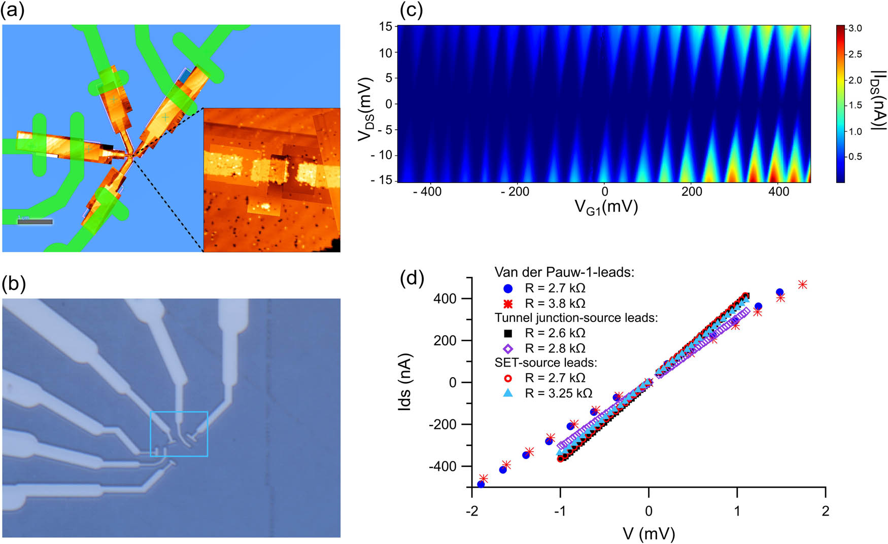
(a) STM image of a patterned SET with designed contacts (green) overlaid on the STM patterned contact pads; inset shows the core device region. (b) Contacts fabricated by EBL and subsequent metallization and anneal; the blue rectangle delimitates the region detailed in (a). (c) Transport measurements on the SET showing coulomb blockade oscillations demonstrating single electron tunneling events. (d) Two-point I–V plots from contact combinations on various devices.
We have implemented and tested the alignment process described in this article on more than 150 multi-terminal devices such as nanowires, tunnel junctions, SETs, and donor dot structures, resulting in better than 95% contact yield. This contact yield is a combination of errors due to contact processes and the alignment processes. We used palladium silicide to contact the buried δ-layer devices and this process has been demonstrated to work with a near 100% contact yield [45]. This alignment strategy has been routinely used on our devices and its effectiveness is evidenced by the successful measurement of coulomb oscillations in SETs, electron loading and unloading in donor dot devices, and measurement of electron tunneling through arrayed atomic-scale features. The combination of this high-yield contact process and a flexible yet reliable alignment process addresses what has been one of the more substantial challenges to successful atomic-scale STM patterned device fabrication. Of the limited number of devices that have failed, known issues with silicon overgrowth and phosphorous dosing were identified. Therefore, we believe that the apparent reduction from 100% in total yield is limited mostly by the device fabrication in UHV including STM patterning, dosing, and silicon encapsulation processes.
For aligning CMOS structures to STM patterned single atom structures it would be desirable to achieve even greater accuracy (on the order of tens of nanometers). To address this, it will likely be necessary to adopt hybrid strategies where the technique described here would be combined with elements from the work of Fuechsle et al. [27] to take advantage of the benefits the two methods offer while mitigating some of the associated disadvantages.
4 Summary and conclusions
We have demonstrated a method to image buried devices with non-contacting electrical mode scanning probe microscopy on surfaces that show no apparent topographical surface perturbations. We developed a multilayer overlaying strategy that provides sufficient accuracy to align complicated contact configurations over buried dopant devices. The method provides reliable re-location of buried devices and determination of coordinates for placement of additional e-beam-defined device components. This methodology allows us to fabricate STM-patterned devices anywhere on a chip without prior registration to any etched fiducial marks during the fabrication stage, with the benefit of saving a significant amount of STM imaging time and yielding flexibility to select suitable areas on the surface free of defects and contaminants. We have achieved an overall contact placement accuracy of 160 nm which we found to be sufficient for integrating various components to the STM fabricated devices such as top gates and coplanar waveguides.
-
Funding information: The authors state no funding involved.
-
Author contributions: All authors have accepted responsibility for the entire content of this manuscript and approved its submission.
-
Conflict of interest: The authors state no conflict of interest.
-
Data availability statement: The data that support the findings of this study are available from the corresponding author upon reasonable request.
References
[1] Fuechsle M, Miwa JA, Mahapatra S, Ryu H, Lee S, Warschkow O, et al. A single-atom transistor. Nat Nanotechnol. 2012;7(4):242–6.10.1038/nnano.2012.21Suche in Google Scholar PubMed
[2] Huff T, Labidi H, Rashidi M, Livadaru L, Dienel T, Achal R, et al. Binary atomic silicon logic. Nat Electron. 2018 Dec;1(12):636–43.10.1038/s41928-018-0180-3Suche in Google Scholar
[3] Wyrick J, Wang X, Kashid RV, Namboodiri P, Schmucker SW, Hagmann JA, et al. Atom-by-atom fabrication of single and few dopant quantum devices. Adv Funct Mater. 2019 Dec;29(52):1903475.10.1002/adfm.201903475Suche in Google Scholar
[4] Wang X, Wyrick J, Kashid RV, Namboodiri P, Schmucker SW, Murphy A, et al. Atomic-scale control of tunneling in donor-based devices. Commun Phys. 2020;3:82.10.1038/s42005-020-0343-1Suche in Google Scholar
[5] Škereň T, Köster SA, Douhard B, Fleischmann C, Fuhrer A. Bipolar device fabrication using a scanning tunnelling microscope. Nat Electron. 2020 Sep;3(9):524–30.10.1038/s41928-020-0445-5Suche in Google Scholar
[6] Wyrick J, Wang X, Namboodiri P, Kashid RV, Fei F, Fox J, et al. Enhanced atomic precision fabrication by adsorption of phosphine into engineered dangling bonds on H–Si using STM and DFT. ACS Nano. 2022 Nov;16(11):19114–23.10.1021/acsnano.2c08162Suche in Google Scholar PubMed
[7] Achal R, Rashidi M, Croshaw J, Churchill D, Taucer M, Huff T, et al. Lithography for robust and editable atomic-scale silicon devices and memories. Nature Commun. 2018 Jul;9(1):2778. [cited 2018 Nov 20]. www.nature.com/naturecommunications.10.1038/s41467-018-05171-ySuche in Google Scholar PubMed PubMed Central
[8] Alipour A, Fowler EL, Moheimani SOR, Owen JHG, Randall JN. Atomic-resolution lithography with an on-chip scanning tunneling microscope. J Vac Sci Technol B. 2022 Apr;40(3):030603.10.1116/6.0001826Suche in Google Scholar
[9] Farzaneha A, Butera RE. Si epitaxy on Cl-Si(100). Appl Surf Sci. 2022 Jul;589:152877.10.1016/j.apsusc.2022.152877Suche in Google Scholar
[10] Scappucci G, Capellini G, Johnston B, Klesse WM, Miwa JA, Simmons MY. A complete fabrication route for atomic-scale, donor-based devices in single-crystal germanium. Nano Lett. 2011 Jun;11(6):2272–9.10.1021/nl200449vSuche in Google Scholar PubMed
[11] Ballard JB, Sisson TW, Owen JHG, Owen WR, Fuchs E, Alexander J, et al. Multimode hydrogen depassivation lithography: A method for optimizing atomically precise write times. J Vac Sci Technol B. 2013 Oct;31(6):06FC01.10.1116/1.4823756Suche in Google Scholar
[12] Usman M, Hill CD, Rahman R, Klimeck G, Simmons MY, Rogge S, et al. Strain and electric field control of hyperfine interactions for donor spin qubits in silicon. Phys Rev B – Condens Matter Mater Phys. 2015;91(24):25–7.10.1103/PhysRevB.91.245209Suche in Google Scholar
[13] He Y, Gorman SK, Keith D, Kranz L, Keizer JG, Simmons MY. A two-qubit gate between phosphorus donor electrons in silicon. Nature. 2019 Jul;571(7765):371–5.10.1038/s41586-019-1381-2Suche in Google Scholar PubMed
[14] Kranz L, Gorman SK, Thorgrimsson B, He Y, Keith D, Keizer JG, et al. Quantum computing: Exploiting a single-crystal environment to minimize the charge noise on qubits in silicon. Adv Mater. 2020;32(40):2070298.10.1002/adma.202003361Suche in Google Scholar PubMed
[15] Fricke L, Hile SJ, Kranz L, Chung Y, He Y, Pakkiam P, et al. Coherent control of a donor-molecule electron spin qubit in silicon. Nat Commun. 2021 Jun;12(1):3323.10.1038/s41467-021-23662-3Suche in Google Scholar PubMed PubMed Central
[16] Kranz L, Gorman SK, Thorgrimsson B, Monir S, He Y, Keith D, et al. The use of exchange coupled atom qubits as atomic-scale magnetic field sensors. Adv Mater. 2023;35(6):2370039.10.1002/adma.202201625Suche in Google Scholar PubMed
[17] Wang X, Khatami E, Fei F, Wyrick J, Namboodiri P, Kashid R, et al. Experimental realization of an extended Fermi-Hubbard model using a 2D lattice of dopant-based quantum dots. Nat Commun. 2022 Nov;13(1):6824.10.1038/s41467-022-34220-wSuche in Google Scholar PubMed PubMed Central
[18] Kiczynski M, Gorman SK, Geng H, Donnelly MB, Chung Y, He Y, et al. Engineering topological states in atom-based semiconductor quantum dots. Nature. 2022 Jun;606(7915):694–9.10.1038/s41586-022-04706-0Suche in Google Scholar PubMed PubMed Central
[19] Salfi J, Mol JA, Rahman R, Klimeck G, Simmons MY, Hollenberg LCL, et al. Quantum simulation of the Hubbard model with dopant atoms in silicon. Nat Commun. 2016;7:1–6.10.1038/ncomms11342Suche in Google Scholar PubMed PubMed Central
[20] Buluta I, Nori F. Quantum simulators. Science. 2009;326(5949):108–11.10.1126/science.1177838Suche in Google Scholar PubMed
[21] Hill CD, Peretz E, Hile SJ, House MG, Fuechsle M, Rogge S, et al. A surface code quantum computer in silicon. 2015;1(9):e150070.10.1126/sciadv.1500707Suche in Google Scholar PubMed PubMed Central
[22] Shen TC, Wang C, Abeln GC, Tucker JR, Lyding JW, Avouris P, et al. Atomic-scale desorption through electronic and vibrational excitation mechanisms. Science. 1995;268:1590.10.1126/science.268.5217.1590Suche in Google Scholar PubMed
[23] Lyding JW, Shen T‐C, Hubacek JS, Tucker JR, Abeln GC. Nanoscale patterning and oxidation of H‐passivated Si(100)‐2×1 surfaces with an ultrahigh vacuum scanning tunneling microscope. Appl Phys Lett. 1994 Apr;64(15):2010–2.10.1063/1.111722Suche in Google Scholar
[24] Walsh MA, Hersam MC. Atomic-scale templates patterned by ultrahigh vacuum scanning tunneling microscopy on silicon. Annu Rev Phys Chem. 2009;60(1):193–216.10.1146/annurev.physchem.040808.090314Suche in Google Scholar PubMed
[25] Schofield SR, Curson NJ, Simmons MY, Rueß FJ, Hallam T, Oberbeck L, et al. Atomically precise placement of single dopants in si. Phys Rev Lett. 2003;91(13):2–5.10.1103/PhysRevLett.91.136104Suche in Google Scholar PubMed
[26] Kranz L, Roche S, Gorman SK, Keizer Joris G, Simmons MY. High-fidelity CNOT gate for donor electron spin qubits in silicon. Phys Rev Appl. 2023 Feb;19(2):024068.10.1103/PhysRevApplied.19.024068Suche in Google Scholar
[27] Fuechsle M, Rueß FJ, Reusch TCG, Mitic M, Simmons MY. Surface gate and contact alignment for buried, atomically precise scanning tunneling microscopy-patterned devices. J Vac Sci Technol B Microelectron Nanometer Struct. 2007;25(6):2562–7.10.1116/1.2781512Suche in Google Scholar
[28] Ruess FJ, Oberbeck L, Simmons MY, Goh KEJ, Hamilton AR, Hallam T, et al. Toward atomic-scale device fabrication in silicon using scanning probe microscopy. Nano Lett. 2004;4(10):1969–73.10.1021/nl048808vSuche in Google Scholar
[29] Bussmann E, Rudolph M, Subramania GS, Misra S, Carr SM, Langlois E, et al. Scanning capacitance microscopy registration of buried atomic-precision donor devices. Nanotechnology. 2015;26(8):085701.10.1088/0957-4484/26/8/085701Suche in Google Scholar PubMed
[30] Ramanayaka AN, Kim HS, Tang K, Wang X, Silver RM, Stewart MD, et al. STM patterned nanowire measurements using photolithographically defined implants in Si(100). Sci Rep. 2018 Dec;8:1790.10.1038/s41598-018-20042-8Suche in Google Scholar PubMed PubMed Central
[31] Gramse G, Kölker A, Lim T, Stock TJZ, Solanki H, Schofield SR, et al. Nondestructive imaging of atomically thin nanostructures buried in silicon. Sci Adv. 2017;3(6):1–9.10.1126/sciadv.1602586Suche in Google Scholar PubMed PubMed Central
[32] Scrymgeour DA, Baca A, Fishgrab K, Simonson RJ, Marshall M, Bussmann E, et al. Determining the resolution of scanning microwave impedance microscopy using atomic-precision buried donor structures. Appl Surf Sci. 2017 Nov;423:1097–102.10.1016/j.apsusc.2017.06.261Suche in Google Scholar
[33] Dagata JA, Schneir J, Harary HH, Evans CJ, Postek MT, Bennett J. Modification of hydrogen-passivated silicon by a scanning tunneling microscope operating in air. Appl Phys Lett. 1990;56(20):2001–3.10.1063/1.102999Suche in Google Scholar
[34] Melitz W, Shen J, Kummel AC, Lee S. Kelvin probe force microscopy and its application. Surf Sci Rep. 2011;66(1):1–27.10.1016/j.surfrep.2010.10.001Suche in Google Scholar
[35] Li C, Minne S, Hu Y, Ma J, He J, Mittel H, et al. PeakForce kelvin probe force microscopy; Bruker Application Note #140. 2021 Sep:1–14Suche in Google Scholar
[36] Li K, Pradeep N, Chikkamaranahalli S, Stan G, Attota R, Fu J, et al. Controlled formation of atomic step morphology on micropatterned Si (100). J Vac Sci Technol B Nanotechnol Microelectron Mater Process Meas Phenom. 2011;29(4):041806.10.1116/1.3610955Suche in Google Scholar
[37] Deng X, Namboodiri P, Li K, Wang X, Stan G, Myers AF, et al. Silicon epitaxy on H-terminated Si (100) surfaces at 250°C. Appl Surf Sci. 2016;378:301–7.10.1016/j.apsusc.2016.03.212Suche in Google Scholar PubMed PubMed Central
[38] Wang X, Hagmann JA, Namboodiri P, Wyrick J, Li K, Murray RE, et al. Quantifying atom-scale dopant movement and electrical activation in Si:P monolayers. Nanoscale. 2018;10(9):4488.10.1039/C7NR07777GSuche in Google Scholar
[39] Bloo ML, Haitjema H, Pril WO. Deformation and wear of pyramidal, silicon-nitride AFM tips scanning micrometre-size features in contact mode. Measurement. 1999 Apr;25(3):203–11.10.1016/S0263-2241(99)00004-4Suche in Google Scholar
[40] Mathew PT, Han W, Rodriguez BJ, Fang F. Structure fabrication on silicon at atomic and close-to-atomic scale using atomic force microscopy: Implications for nanopatterning and nanodevice fabrication. Micromachines. 2022 Apr;13(4):524.10.3390/mi13040524Suche in Google Scholar PubMed PubMed Central
[41] Avouris P, Hertel T, Martel R. Atomic force microscope tip-induced local oxidation of silicon: kinetics, mechanism, and nanofabrication. Appl Phys Lett. 1997 Jul;71(2):285–7.10.1063/1.119521Suche in Google Scholar
[42] Tello M, Garcı́a R. Nano-oxidation of silicon surfaces: Comparison of noncontact and contact atomic-force microscopy methods. Appl Phys Lett. 2001 Jul;79(3):424–6.10.1063/1.1385582Suche in Google Scholar
[43] Snow ES, Campbell PM. Fabrication of Si nanostructures with an atomic force microscope. Appl Phys Lett. 1994 Apr;64(15):1932–4.10.1063/1.111746Suche in Google Scholar
[44] Wyrick JE. ABDNavigator and ABDController [Internet]. GitHub; 2020. https://github.com/usnistgov/ABDNavigator.Suche in Google Scholar
[45] Schmucker SW, Namboodiri PN, Kashid R, Wang X, Hu B, Wyrick JE, et al. Low-resistance, high-yield electrical contacts to atom scale Si:P devices using palladium silicide. Phys Rev Appl. 2019 Mar;11(3):034071.10.1103/PhysRevApplied.11.034071Suche in Google Scholar PubMed PubMed Central
[46] Staring AAM, Williamson JG, Van Houten H, Beenakker CWJ, Kouwenhoven LP, Foxon CT. Coulomb-blockade oscillations in a quantum dot. Phys B Condens Matter. 1991 Dec;175(1–3):226–30.10.1016/0921-4526(91)90717-SSuche in Google Scholar
© 2024 the author(s), published by De Gruyter
This work is licensed under the Creative Commons Attribution 4.0 International License.
Artikel in diesem Heft
- Research Articles
- Tension buckling and postbuckling of nanocomposite laminated plates with in-plane negative Poisson’s ratio
- Polyvinylpyrrolidone-stabilised gold nanoparticle coatings inhibit blood protein adsorption
- Energy and mass transmission through hybrid nanofluid flow passing over a spinning sphere with magnetic effect and heat source/sink
- Surface treatment with nano-silica and magnesium potassium phosphate cement co-action for enhancing recycled aggregate concrete
- Numerical investigation of thermal radiation with entropy generation effects in hybrid nanofluid flow over a shrinking/stretching sheet
- Enhancing the performance of thermal energy storage by adding nano-particles with paraffin phase change materials
- Using nano-CaCO3 and ceramic tile waste to design low-carbon ultra high performance concrete
- Numerical analysis of thermophoretic particle deposition in a magneto-Marangoni convective dusty tangent hyperbolic nanofluid flow – Thermal and magnetic features
- Dual numerical solutions of Casson SA–hybrid nanofluid toward a stagnation point flow over stretching/shrinking cylinder
- Single flake homo p–n diode of MoTe2 enabled by oxygen plasma doping
- Electrostatic self-assembly effect of Fe3O4 nanoparticles on performance of carbon nanotubes in cement-based materials
- Multi-scale alignment to buried atom-scale devices using Kelvin probe force microscopy
- Antibacterial, mechanical, and dielectric properties of hydroxyapatite cordierite/zirconia porous nanocomposites for use in bone tissue engineering applications
- Time-dependent Darcy–Forchheimer flow of Casson hybrid nanofluid comprising the CNTs through a Riga plate with nonlinear thermal radiation and viscous dissipation
- Durability prediction of geopolymer mortar reinforced with nanoparticles and PVA fiber using particle swarm optimized BP neural network
- Utilization of zein nano-based system for promoting antibiofilm and anti-virulence activities of curcumin against Pseudomonas aeruginosa
- Antibacterial effect of novel dental resin composites containing rod-like zinc oxide
- An extended model to assess Jeffery–Hamel blood flow through arteries with iron-oxide (Fe2O3) nanoparticles and melting effects: Entropy optimization analysis
- Comparative study of copper nanoparticles over radially stretching sheet with water and silicone oil
- Cementitious composites modified by nanocarbon fillers with cooperation effect possessing excellent self-sensing properties
- Confinement size effect on dielectric properties, antimicrobial activity, and recycling of TiO2 quantum dots via photodegradation processes of Congo red dye and real industrial textile wastewater
- Biogenic silver nanoparticles of Moringa oleifera leaf extract: Characterization and photocatalytic application
- Novel integrated structure and function of Mg–Gd neutron shielding materials
- Impact of multiple slips on thermally radiative peristaltic transport of Sisko nanofluid with double diffusion convection, viscous dissipation, and induced magnetic field
- Magnetized water-based hybrid nanofluid flow over an exponentially stretching sheet with thermal convective and mass flux conditions: HAM solution
- A numerical investigation of the two-dimensional magnetohydrodynamic water-based hybrid nanofluid flow composed of Fe3O4 and Au nanoparticles over a heated surface
- Development and modeling of an ultra-robust TPU-MWCNT foam with high flexibility and compressibility
- Effects of nanofillers on the physical, mechanical, and tribological behavior of carbon/kenaf fiber–reinforced phenolic composites
- Polymer nanocomposite for protecting photovoltaic cells from solar ultraviolet in space
- Study on the mechanical properties and microstructure of recycled concrete reinforced with basalt fibers and nano-silica in early low-temperature environments
- Synergistic effect of carbon nanotubes and polyvinyl alcohol on the mechanical performance and microstructure of cement mortar
- CFD analysis of paraffin-based hybrid (Co–Au) and trihybrid (Co–Au–ZrO2) nanofluid flow through a porous medium
- Forced convective tangent hyperbolic nanofluid flow subject to heat source/sink and Lorentz force over a permeable wedge: Numerical exploration
- Physiochemical and electrical activities of nano copper oxides synthesised via hydrothermal method utilising natural reduction agents for solar cell application
- A homotopic analysis of the blood-based bioconvection Carreau–Yasuda hybrid nanofluid flow over a stretching sheet with convective conditions
- In situ synthesis of reduced graphene oxide/SnIn4S8 nanocomposites with enhanced photocatalytic performance for pollutant degradation
- A coarse-grained Poisson–Nernst–Planck model for polyelectrolyte-modified nanofluidic diodes
- A numerical investigation of the magnetized water-based hybrid nanofluid flow over an extending sheet with a convective condition: Active and passive controls of nanoparticles
- The LyP-1 cyclic peptide modified mesoporous polydopamine nanospheres for targeted delivery of triptolide regulate the macrophage repolarization in atherosclerosis
- Synergistic effect of hydroxyapatite-magnetite nanocomposites in magnetic hyperthermia for bone cancer treatment
- The significance of quadratic thermal radiative scrutinization of a nanofluid flow across a microchannel with thermophoretic particle deposition effects
- Ferromagnetic effect on Casson nanofluid flow and transport phenomena across a bi-directional Riga sensor device: Darcy–Forchheimer model
- Performance of carbon nanomaterials incorporated with concrete exposed to high temperature
- Multicriteria-based optimization of roller compacted concrete pavement containing crumb rubber and nano-silica
- Revisiting hydrotalcite synthesis: Efficient combined mechanochemical/coprecipitation synthesis to design advanced tunable basic catalysts
- Exploration of irreversibility process and thermal energy of a tetra hybrid radiative binary nanofluid focusing on solar implementations
- Effect of graphene oxide on the properties of ternary limestone clay cement paste
- Improved mechanical properties of graphene-modified basalt fibre–epoxy composites
- Sodium titanate nanostructured modified by green synthesis of iron oxide for highly efficient photodegradation of dye contaminants
- Green synthesis of Vitis vinifera extract-appended magnesium oxide NPs for biomedical applications
- Differential study on the thermal–physical properties of metal and its oxide nanoparticle-formed nanofluids: Molecular dynamics simulation investigation of argon-based nanofluids
- Heat convection and irreversibility of magneto-micropolar hybrid nanofluids within a porous hexagonal-shaped enclosure having heated obstacle
- Numerical simulation and optimization of biological nanocomposite system for enhanced oil recovery
- Laser ablation and chemical vapor deposition to prepare a nanostructured PPy layer on the Ti surface
- Cilostazol niosomes-loaded transdermal gels: An in vitro and in vivo anti-aggregant and skin permeation activity investigations towards preparing an efficient nanoscale formulation
- Linear and nonlinear optical studies on successfully mixed vanadium oxide and zinc oxide nanoparticles synthesized by sol–gel technique
- Analytical investigation of convective phenomena with nonlinearity characteristics in nanostratified liquid film above an inclined extended sheet
- Optimization method for low-velocity impact identification in nanocomposite using genetic algorithm
- Analyzing the 3D-MHD flow of a sodium alginate-based nanofluid flow containing alumina nanoparticles over a bi-directional extending sheet using variable porous medium and slip conditions
- A comprehensive study of laser irradiated hydrothermally synthesized 2D layered heterostructure V2O5(1−x)MoS2(x) (X = 1–5%) nanocomposites for photocatalytic application
- Computational analysis of water-based silver, copper, and alumina hybrid nanoparticles over a stretchable sheet embedded in a porous medium with thermophoretic particle deposition effects
- A deep dive into AI integration and advanced nanobiosensor technologies for enhanced bacterial infection monitoring
- Effects of normal strain on pyramidal I and II 〈c + a〉 screw dislocation mobility and structure in single-crystal magnesium
- Computational study of cross-flow in entropy-optimized nanofluids
- Significance of nanoparticle aggregation for thermal transport over magnetized sensor surface
- A green and facile synthesis route of nanosize cupric oxide at room temperature
- Effect of annealing time on bending performance and microstructure of C19400 alloy strip
- Chitosan-based Mupirocin and Alkanna tinctoria extract nanoparticles for the management of burn wound: In vitro and in vivo characterization
- Electrospinning of MNZ/PLGA/SF nanofibers for periodontitis
- Photocatalytic degradation of methylene blue by Nd-doped titanium dioxide thin films
- Shell-core-structured electrospinning film with sequential anti-inflammatory and pro-neurogenic effects for peripheral nerve repairment
- Flow and heat transfer insights into a chemically reactive micropolar Williamson ternary hybrid nanofluid with cross-diffusion theory
- One-pot fabrication of open-spherical shapes based on the decoration of copper sulfide/poly-O-amino benzenethiol on copper oxide as a promising photocathode for hydrogen generation from the natural source of Red Sea water
- A penta-hybrid approach for modeling the nanofluid flow in a spatially dependent magnetic field
- Advancing sustainable agriculture: Metal-doped urea–hydroxyapatite hybrid nanofertilizer for agro-industry
- Utilizing Ziziphus spina-christi for eco-friendly synthesis of silver nanoparticles: Antimicrobial activity and promising application in wound healing
- Plant-mediated synthesis, characterization, and evaluation of a copper oxide/silicon dioxide nanocomposite by an antimicrobial study
- Effects of PVA fibers and nano-SiO2 on rheological properties of geopolymer mortar
- Investigating silver and alumina nanoparticles’ impact on fluid behavior over porous stretching surface
- Potential pharmaceutical applications and molecular docking study for green fabricated ZnO nanoparticles mediated Raphanus sativus: In vitro and in vivo study
- Effect of temperature and nanoparticle size on the interfacial layer thickness of TiO2–water nanofluids using molecular dynamics
- Characteristics of induced magnetic field on the time-dependent MHD nanofluid flow through parallel plates
- Flexural and vibration behaviours of novel covered CFRP composite joints with an MWCNT-modified adhesive
- Experimental research on mechanically and thermally activation of nano-kaolin to improve the properties of ultra-high-performance fiber-reinforced concrete
- Analysis of variable fluid properties for three-dimensional flow of ternary hybrid nanofluid on a stretching sheet with MHD effects
- Biodegradability of corn starch films containing nanocellulose fiber and thymol
- Toxicity assessment of copper oxide nanoparticles: In vivo study
- Some measures to enhance the energy output performances of triboelectric nanogenerators
- Reinforcement of graphene nanoplatelets on water uptake and thermomechanical behaviour of epoxy adhesive subjected to water ageing conditions
- Optimization of preparation parameters and testing verification of carbon nanotube suspensions used in concrete
- Max-phase Ti3SiC2 and diverse nanoparticle reinforcements for enhancement of the mechanical, dynamic, and microstructural properties of AA5083 aluminum alloy via FSP
- Advancing drug delivery: Neural network perspectives on nanoparticle-mediated treatments for cancerous tissues
- PEG-PLGA core–shell nanoparticles for the controlled delivery of picoplatin–hydroxypropyl β-cyclodextrin inclusion complex in triple-negative breast cancer: In vitro and in vivo study
- Conduction transportation from graphene to an insulative polymer medium: A novel approach for the conductivity of nanocomposites
- Review Articles
- Developments of terahertz metasurface biosensors: A literature review
- Overview of amorphous carbon memristor device, modeling, and applications for neuromorphic computing
- Advances in the synthesis of gold nanoclusters (AuNCs) of proteins extracted from nature
- A review of ternary polymer nanocomposites containing clay and calcium carbonate and their biomedical applications
- Recent advancements in polyoxometalate-functionalized fiber materials: A review
- Special contribution of atomic force microscopy in cell death research
- A comprehensive review of oral chitosan drug delivery systems: Applications for oral insulin delivery
- Cellular senescence and nanoparticle-based therapies: Current developments and perspectives
- Cyclodextrins-block copolymer drug delivery systems: From design and development to preclinical studies
- Micelle-based nanoparticles with stimuli-responsive properties for drug delivery
- Critical assessment of the thermal stability and degradation of chemically functionalized nanocellulose-based polymer nanocomposites
- Research progress in preparation technology of micro and nano titanium alloy powder
- Nanoformulations for lysozyme-based additives in animal feed: An alternative to fight antibiotic resistance spread
- Incorporation of organic photochromic molecules in mesoporous silica materials: Synthesis and applications
- A review on modeling of graphene and associated nanostructures reinforced concrete
- A review on strengthening mechanisms of carbon quantum dots-reinforced Cu-matrix nanocomposites
- Review on nanocellulose composites and CNFs assembled microfiber toward automotive applications
- Nanomaterial coating for layered lithium rich transition metal oxide cathode for lithium-ion battery
- Application of AgNPs in biomedicine: An overview and current trends
- Nanobiotechnology and microbial influence on cold adaptation in plants
- Hepatotoxicity of nanomaterials: From mechanism to therapeutic strategy
- Applications of micro-nanobubble and its influence on concrete properties: An in-depth review
- A comprehensive systematic literature review of ML in nanotechnology for sustainable development
- Exploiting the nanotechnological approaches for traditional Chinese medicine in childhood rhinitis: A review of future perspectives
- Twisto-photonics in two-dimensional materials: A comprehensive review
- Current advances of anticancer drugs based on solubilization technology
- Recent process of using nanoparticles in the T cell-based immunometabolic therapy
- Future prospects of gold nanoclusters in hydrogen storage systems and sustainable environmental treatment applications
- Preparation, types, and applications of one- and two-dimensional nanochannels and their transport properties for water and ions
- Microstructural, mechanical, and corrosion characteristics of Mg–Gd–x systems: A review of recent advancements
- Functionalized nanostructures and targeted delivery systems with a focus on plant-derived natural agents for COVID-19 therapy: A review and outlook
- Mapping evolution and trends of cell membrane-coated nanoparticles: A bibliometric analysis and scoping review
- Nanoparticles and their application in the diagnosis of hepatocellular carcinoma
- In situ growth of carbon nanotubes on fly ash substrates
- Structural performance of boards through nanoparticle reinforcement: An advance review
- Reinforcing mechanisms review of the graphene oxide on cement composites
- Seed regeneration aided by nanomaterials in a climate change scenario: A comprehensive review
- Surface-engineered quantum dot nanocomposites for neurodegenerative disorder remediation and avenue for neuroimaging
- Graphitic carbon nitride hybrid thin films for energy conversion: A mini-review on defect activation with different materials
- Nanoparticles and the treatment of hepatocellular carcinoma
- Special Issue on Advanced Nanomaterials and Composites for Energy Conversion and Storage - Part II
- Highly safe lithium vanadium oxide anode for fast-charging dendrite-free lithium-ion batteries
- Recent progress in nanomaterials of battery energy storage: A patent landscape analysis, technology updates, and future prospects
- Special Issue on Advanced Nanomaterials for Carbon Capture, Environment and Utilization for Energy Sustainability - Part II
- Calcium-, magnesium-, and yttrium-doped lithium nickel phosphate nanomaterials as high-performance catalysts for electrochemical water oxidation reaction
- Low alkaline vegetation concrete with silica fume and nano-fly ash composites to improve the planting properties and soil ecology
- Mesoporous silica-grafted deep eutectic solvent-based mixed matrix membranes for wastewater treatment: Synthesis and emerging pollutant removal performance
- Electrochemically prepared ultrathin two-dimensional graphitic nanosheets as cathodes for advanced Zn-based energy storage devices
- Enhanced catalytic degradation of amoxicillin by phyto-mediated synthesised ZnO NPs and ZnO-rGO hybrid nanocomposite: Assessment of antioxidant activity, adsorption, and thermodynamic analysis
- Incorporating GO in PI matrix to advance nanocomposite coating: An enhancing strategy to prevent corrosion
- Synthesis, characterization, thermal stability, and application of microporous hyper cross-linked polyphosphazenes with naphthylamine group for CO2 uptake
- Engineering in ceramic albite morphology by the addition of additives: Carbon nanotubes and graphene oxide for energy applications
- Nanoscale synergy: Optimizing energy storage with SnO2 quantum dots on ZnO hexagonal prisms for advanced supercapacitors
- Aging assessment of silicone rubber materials under corona discharge accompanied by humidity and UV radiation
- Tuning structural and electrical properties of Co-precipitated and Cu-incorporated nickel ferrite for energy applications
- Sodium alginate-supported AgSr nanoparticles for catalytic degradation of malachite green and methyl orange in aqueous medium
- An environmentally greener and reusability approach for bioenergy production using Mallotus philippensis (Kamala) seed oil feedstock via phytonanotechnology
- Micro-/nano-alumina trihydrate and -magnesium hydroxide fillers in RTV-SR composites under electrical and environmental stresses
- Mechanism exploration of ion-implanted epoxy on surface trap distribution: An approach to augment the vacuum flashover voltages
- Nanoscale engineering of semiconductor photocatalysts boosting charge separation for solar-driven H2 production: Recent advances and future perspective
- Excellent catalytic performance over reduced graphene-boosted novel nanoparticles for oxidative desulfurization of fuel oil
- Special Issue on Advances in Nanotechnology for Agriculture
- Deciphering the synergistic potential of mycogenic zinc oxide nanoparticles and bio-slurry formulation on phenology and physiology of Vigna radiata
- Nanomaterials: Cross-disciplinary applications in ornamental plants
- Special Issue on Catechol Based Nano and Microstructures
- Polydopamine films: Versatile but interface-dependent coatings
- In vitro anticancer activity of melanin-like nanoparticles for multimodal therapy of glioblastoma
- Poly-3,4-dihydroxybenzylidenhydrazine, a different analogue of polydopamine
- Chirality and self-assembly of structures derived from optically active 1,2-diaminocyclohexane and catecholamines
- Advancing resource sustainability with green photothermal materials: Insights from organic waste-derived and bioderived sources
- Bioinspired neuromelanin-like Pt(iv) polymeric nanoparticles for cancer treatment
- Special Issue on Implementing Nanotechnology for Smart Healthcare System
- Intelligent explainable optical sensing on Internet of nanorobots for disease detection
- Special Issue on Green Mono, Bi and Tri Metallic Nanoparticles for Biological and Environmental Applications
- Tracking success of interaction of green-synthesized Carbopol nanoemulgel (neomycin-decorated Ag/ZnO nanocomposite) with wound-based MDR bacteria
- Green synthesis of copper oxide nanoparticles using genus Inula and evaluation of biological therapeutics and environmental applications
- Biogenic fabrication and multifunctional therapeutic applications of silver nanoparticles synthesized from rose petal extract
- Metal oxides on the frontlines: Antimicrobial activity in plant-derived biometallic nanoparticles
- Controlling pore size during the synthesis of hydroxyapatite nanoparticles using CTAB by the sol–gel hydrothermal method and their biological activities
- Special Issue on State-of-Art Advanced Nanotechnology for Healthcare
- Applications of nanomedicine-integrated phototherapeutic agents in cancer theranostics: A comprehensive review of the current state of research
- Smart bionanomaterials for treatment and diagnosis of inflammatory bowel disease
- Beyond conventional therapy: Synthesis of multifunctional nanoparticles for rheumatoid arthritis therapy