Application of helium ion microscopy to nanostructured polymer materials
-
Valery N. Bliznyuk
Valery Bliznyuk is a research associate at the Department of Environmental Engineering and Earth Science, Clemson University. He received a PhD degree in Polymer Science from the Institute of Macromolecular Chemistry of National Academy of Sciences, Kiev, Ukraine (1985), and a DSc degree in Polymer Chemistry in the field of nanostructured organic materials from Kiev State University (2004). He worked as a researcher in Ukraine, Germany (Alexander von Humboldt Foundation fellow, University of Mainz), England (University of Cambridge and University of Oxford), and the USA. He is a coauthor of more than 140 peer reviewed publications and several reviews in the field of nanostructured materials and their characterization. His research is focused on development of advanced polymer materials for molecular electronics, photovoltaics, and sensors.
 ,
Dennis LaJeunesse
,
Dennis LaJeunesse
Dennis LaJeunesse is an Associate Professor in the Department of Nanoscience at the Joint School of Nanoscience and Nanoengineering at the University of North Carolina Greensboro. He received a PhD degree in Biology from Johns Hopkins University in 1995. His current research focuses on using genetics approaches to characterize biological nanoscale structures/surfaces and identifying the mechanisms underlying the formation of biological nanostructures. In addition to traditional genetic and molecular techniques, Dr. LaJeunesse also uses several ultrahigh-resolution microscopic techniques such as helium ion microscopy and focused ion beam milling/SEM for his research. A central theme in this research is to determine the biological and mechanical roles of the polysaccharide chitin in living systems using several genetic model organisms including
Drosophila melanogaster andSaccharomyces cerevisiae. Adam Boseman is presently a PhD candidate in the Department of Nanoscience at the Joint School of Nanoscience and Nanoengineering at the University of North Carolina Greensboro. He received his BS in Applied Mathematics from the University of North Carolina at Greensboro in 2009. Adam is deeply involved in HIM and FIB/SEM-based studies of biological systems. His research deals with biomimetic nanotechnology focusing primarily on the development of nanopatterned surfaces found on the cornea of
Drosophila melanogaster .

Abstract
Helium ion microscopy (HIM) is a relatively new high-resolution nanotechnology imaging and nanofabrication tool. HIM offers a near-molecular resolution (approaching that of TEM) combined with a simplicity of sample preparation and high depth of field similar to SEM. Simultaneously, the technique is not limited by the surface roughness as scanning probe microscopy (SPM) techniques or by the surface charging or radiation damage like SEM. In our review, we consider general principles, advantages, and prospects of HIM application in polymer science. Examples of high-resolution imaging of polymer-based nanocomposites, polymer nanoparticles, nanofibers, nanoporous materials, polymer nanocrystals, biopolymers, and polymer-based photovoltaic and sensor devices are presented. We compare the HIM’s applicability with other modern imaging techniques: SPM and SEM.
1 Introduction
Modern nanotechnology revolution would not be possible without the development of three key components: nanofabrication techniques and approaches; methods of nanoscale structure and physical properties characterization, and high-performance multifunctional materials. Moreover, progress in development of advanced nanostructured materials depends strongly on the development of the first two key components. For instance, the discovery of C60 and carbon nanotubes required the application of new laser ablation techniques and of high-resolution electron microscopy [1]. The invention of scanning probe microscopy (SPM) techniques in the 1980s brought a wide spectrum of new nanoscale characterization and nanofabrication tools that enabled in situ measurements of the stiffness and thermal conductivity of nanotubes and the single-electron transfer properties of metallic nanoparticles [2]. SPM measurements of intermolecular interactions and deeper understanding of adhesion and friction phenomena allowed further development of microelectromechanical systems (MEMS) and sensors.
Our century is the century of organic materials and biomaterials. Polymers play a unique and increasing role in the modern world and technology progress. They are used for an enormously diverse range of applications spanning from packaging materials, adhesives, and paints to medical implants, components of modern computers, batteries and other electronic devices, lightweight impact-resistant composites applied in alternative energy systems, construction, and transportation. Not surprisingly the worldwide production of polymers per unit volume has already exceeded that of metals [3].
It is not only their unique applications that make polymers so fascinating, polymers play an inherent role in life on earth as well. DNA, which contains the genetic code of any living species, and which is without any doubt “the most important molecule” on the Earth is a polymer; moreover, proteins and other components of living cells such as polysaccharides are all examples of natural polymer materials. Such biopolymers play crucial roles in many modern bionanotechnologies, and the impact of the use of these biopolymers has just been approached. Many biopolymers exhibit fascinating properties such as biomolecular recognition and self-assembly creating the possibility for new biodegradable, biocompatible, and bioinspired materials in the near future. The biomaterials will be used in countless applications including biosensor devices, targeted assembly and drug delivery, tissue engineering and regeneration, implant materials, smart stimuli responsive surfaces, artificial neuron networks and adaptive systems, bioelectronics, and bio-MEMS [4–7].
Imaging techniques have played an important role throughout the history of polymer materials science and engineering and will continue to do so as we progress toward the application of new and novel polymeric materials including biopolymer and bioinspired polymers. Recent examples of the importance of imaging for polymer science is demonstrated by the classification of mesophases in polymer liquid crystals, which became possible with polarization optical microscopy [8], understanding of the crystalline organization of polyethylene and other crystalline polymers using transmission electron microscopy [9], and formation of various domain structures due to self-organization in block copolymers [10].
Many polymers are inherently nanostructured materials with a complex multilevel hierarchical structural organization [11]. The elementary structural unit of the polymer chains – monomer has typically nanoscale dimensions (0.5–10 nm). The basic structural element of organic polymers is the carbon atom, which has four valence electrons. This allows numerous ways of interconnection of monomer units producing high variety of structural architectures. On a macromolecular level (∼20–100 nm) of the structural organization of polymer chains, this is manifested as distinct molecular configurations (linear, branched, dendritic, comb-like, networks, macrocircular, etc.) and several standard molecular conformations (i.e., physical shapes). The correspondence of the latter to the minimum of energy determines the ability of particular polymer chains to form a crystalline or amorphous phase depending on the temperature and composition. So-called random coil conformation (with a typical length scale – the radius of gyration in the range of 20–100 nm depending on the molecular mass) and more compact globule conformation are characteristic features of polymers in amorphous or solution states. Ordered zig-zag (or more generally helical) conformations allow higher packing density of the chains required for formation of a crystalline phase. The so-called folding conformation is the next level of the structural organization of crystallizable polymers. Folding of the polymer chains determines the size and shapes of their crystalline lamellas – the basic unit of their structure at 30- to 3000-nm scale. At the opposite “top side” of their hierarchical organization, crystalline polymers are typically represented by spherulites. The spherulites are relatively large features (10–1000 μm) constructed by several beams of crystalline lamellaes running away from a common focal point and interlaced with an amorphous phase.
More rigid polymer chains (or ones with relatively bulky rigid side groups) can be found in several additional phase states, so-called liquid-crystalline (LC) phase or phases with a reduced order parameter [12]. Typical for this class of polymers is a uniform orientation of polymer chains or their mesogenic side groups within nano- to micrometer size domains. Owing to such orientation, LC polymers can be organized in high-modulus fibers like the famous polymer Kevlar of bullet proof vests, Nomex, and others. Multicomponent systems introduce an additional variety to supramolecular organization in polymer materials: polymer blends and copolymers. In this case, the morphology depends also on the intermolecular interactions between the components. The characteristic domain-like morphology, which appears as a result of phase separation in the system, can be controlled by the composition and mobility of polymer chains (processing temperature, chemical crosslinking, etc.).
The structure of the polymer materials described above has been characterized with particle beam microscopic techniques such as transmission and scanning electron microscopy (TEM and SEM) and more recently with SPM techniques such as atomic force microscopy (AFM). Both classes of microscopy techniques offer molecular level resolution but are principally different in their underlying physical nature and technical characteristics [7, 9, 10, 13, 14].
The electron microscopy (EM) techniques involves the application of an electron beam, i.e., a flux of electrons which are accelerated in vacuum and then transmitted or scattered by a specimen to provide information about its structural organization. The electrons can be considered as a wave in quantum mechanics, which makes the technique similar to a traditional light microscopy (just with much higher resolution). In addition to morphological investigation, electron microscopy allows additional information such as elemental analysis, diffraction testing of crystalline symmetry, and orientation of polymer chains. The SPM technique employs an entirely different principle in its application and detection. SPM measures the interatomic interaction forces between a sharp tip (probe) and a surface of interest. By scanning a surface with a precise piezo-element, the probe/surface interaction collects information of the physical interactions between the two components that is dependent on the probe position and the probe-sample separation distance. The resolution in the case of SPM techniques depends primarily on the sharpness of the probe tip. Distinguishing between different types of electromagnetic interaction allows measuring physical properties of the surface (such as stiffness, adhesion, electrostatic or magnetic field distribution) at nanoscale and in its relation to the morphology.
Despite the high level of development and application, both EM and SPM techniques suffer some drawbacks in the study of many polymers. Sample preparation protocols especially those found in TEM can alter the sample itself. Furthermore, imaging polymeric samples is problematic as most of polymers are composed of highly insulating materials that accumulate charges under an electron beam exposure thus resulting in a poor resolution. Due to this reason polymer materials cannot be imaged in their native state in the majority of cases.
Unlike EM techniques, which require elaboration of special sample preparation protocols changing the nature of the sample, such as the application of metallic coatings, SPM techniques can be applied to polymer samples in their native state and often in situ as well. SPM is a powerful tool for the analysis of surface properties of a material, but is limited by the general principle that governs the SPM technique itself. Owing to the limited presentation angle of the probe, information from surfaces with irregular or high aspect ratio features cannot be acquired accurately, thus, limiting the ability of investigation of some polymer materials [14]. Another problem arises from the almost atomically sharp SPM probe indenter, which can insert a giga-Pascal-scale pressure to the polymer surface even with relatively low (nano-Newton scale) forces applied during scanning, which can be destructive for many polymers, especially biopolymers. This problem can be partially overcome by application of special noncontact modes of scanning or by scanning in a liquid environment (which eliminates capillary forces contribution), but at the expense of technique’s nanoscale resolution.
2 HIM experimental setup
The setup and principle of operation of helium ion microscopy (HIM) is similar to that of scanning electron microscope (SEM) [15–20]. The HIM column consists of two focusing lenses and a system of octopoles to produce scanning the ion beam over an area of the sample (Figure 1). It features also a number of quadrupoles for the ion beam alignment and astigmatism correction. Unlike an SEM device that uses an electron gun, the HIM has an ion gun as a source of charged particles, which are accelerated in vacuum by application of high voltage (typically, 10–35 keV) to provide a focused beam with a variable landing energy. However, due to the opposite (i.e., positive) sign of the accelerated particles, the gun is used as an anode instead of a cathode as in the case of the SEM technique.
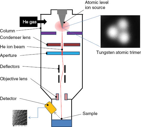
Schematic of a helium ion microscope.
The first ion-beam microscope was invented more than half a century ago and consisted of a sharp metallic needle put in vacuum [20–22]. Under application of high voltage to the needle, metallic atoms from the needle apex could be emitted and then visualized on a scintillation screen. That first device was known as a field ion microscope (FIM) and was the first microscopic system permitting direct visualization of atoms. The main limitation of the FIM was that only the structure of metals that were located on the top of the needle end could be visualized. Further development of FIM allowed application of high-voltage pulses to “shake off” atoms from the needle layer by layer in order to visualize the structure of a thin surface film. The latter technique received the name of a 3D atom probe microscopy. The FIM and 3D atom probe microscopy have been applied to study the shape, crystallography, and composition of samples, which have been prepared into needle-like shapes or built on the top (adsorbed) of a metallic needle.
The probing of a sample surface with ions in a microscope device can be performed in two distinct ways: either by broad illumination of an area by an ion beam or by scanning a surface in a raster manner similarly to an SEM setup [22]. Geometrically related analytical information can be then extracted from the surface of interest using one of two basic methods: imaging microanalysis, which can be accomplished with a stigmatic, analytical emission ion microscope (EIM), or via a scanning ion microscope setup. In the second case scenario, the ion microscope is combined with secondary ion mass spectrometry (SIMS) analysis, which involves the analysis and separation of the emitted secondary ions based on their charge to mass ratios and provides mass and/or isotopic information about the sample. A scanning ion microprobe instrument developed at the University of Chicago in the 1980s enabled SIMS imaging and microanalysis of materials with a sub-100-nm range lateral resolution [22]. This unique instrument has been applied in various fields including fundamental biological studies, biopolymers, and paleontology [23].
Historically, scanning ion microscopes appeared later than the EIM types. Noble gas ions or reactive ions such as those of oxygen and cesium have been used to induce and promote secondary ion emission in both types of the ion microscopes. However, a big step in the improvement of the spatial resolution (down to 10 nm) of such devices was associated with application of heavy-ion probes (such as Ga+, In+, Au+, etc.) extracted from liquid metal ion sources (LMIS) [24, 25].
The focused ion microscope in its present state was recently reinvented when a bright He ion source was developed by ALIS Corporation (a Carl Zeiss SMT AG Company) [11]. The innovative technology became technically possible when a sharp metallic electrode was inserted into a low-pressure He gas chamber (similar to FIM technique) to produce helium ions that then could be focused onto a sample surface (Figure 1). In the case of the Zeiss Orion HIM, the source consists of a fine tungsten needle. In this revised source, a high voltage is applied to the needle and concentrated on just a few apex atoms in the form of a so-called “trimer” (Figure 1). The tungsten trimer serves as the source for the ionization of He atoms and preferentially ionizes the He atoms rather than itself. So-called surface disks located in the space around each metal atom in the trimer prove a renewable and sustainable nanosource of He ions. Depending on the He gas pressure, the brightness of the nanosources can be regulated. Owing to the applied high-voltage, He ions are accelerated in the vacuum column while traveling the same trajectories determined by the position of the apex atoms. The number of such nanosources on the metal probe is limited to just three atoms via short time application of higher voltage that removes unnecessary, extraneous tungsten atoms from the probe’s apex; just one of the three atomic sources will be used for scanning over the sample of interest by application of an aperture. Altogether, this produces a stable nearly atomically sharp beam of He ions. The virtual source size can be estimated as ∼3 angstroms [18], which enables very high brightness (4×10⁹ A/cm2 sr) at an extraction voltage of about 25 keV.
Application of a large positive voltage to the ion-generating source located at the tip of the metallic probe generates a local electric field of several volts per angstrom. Moreover, this voltage needs to be precisely adjusted so that the field is not quite sufficient to remove the apex atoms but sufficient enough to cause polarization of He atoms in a vicinity via a created electric field gradient. The polarized He atoms are drawn toward the apex surface due to the local electric field near the apex. When they approach the region of the maximum electric field, they ionize due to high probability of electron tunneling from the He outermost electron shell to the metal electrode. Thus, He+ ions are produced and then accelerated in the vacuum column to produce a narrow beam. The region near an apex atom where it happens is called the ionization disc. In fact, each of the apex atoms in the trimer will have its own ionizing disc and will be a source of an individual He+ beam. However, as mentioned earlier, only one of the ion beams will be selected with an aperture, focused, and used for scanning across the sample.
Physical properties of HIM as an imaging system are determined by several factors. Similarly to electron microscopy, the resolution of HIM is limited by interference phenomenon due to scattering of waves at different points on the sample (the diffraction limit). In both cases, the wavelength of the imaging beam of particles is determined in accordance to de Broglie equation:
where λ is the wavelength, h is Planck’s constant, m is the mass of a particle moving at a velocity v, E is the particle’s kinetic energy, and V is the applied acceleration voltage. This equation shows a key advantage of HIM over other wave-based microscopy techniques: very short wavelength. Because the mass of He is ∼104 times higher than the mass of the electron, their wavelength is 100 times smaller assuming the same accelerating voltage applied [15–20].
Therefore, application of He ions instead of electrons has the advantage of a dramatic reduction of the diffraction effect allowing focusing the ion beam into much smaller probe size. This, at least in theory, will permit high-resolution imaging with a lower energy beam. In accordance to previous publications [18], the optical characteristics of He ion source can be summarized as: 1) brightness ∼109 A cm-2 sr-1 (calculated); 2) energy spread ∼1 eV (measured), and beam current of 0.5 pA (for landing energy about 25 keV and working distance of 6 mm). Comparing these parameters of a helium ion beam to the electron beam of a standard SEM, we find that a brightness of a SEM beam produced by a typical LaB6 cathode source is two orders of magnitude lower than an HIM, but is roughly the same if a special (and expensive) cold field emission cathode is used [7], while the energy spread is similar for both devices when compared to an He ion beam. The probe current in SEM is ∼1 μA and ∼2 nA for LaB6 and cold field emission cathodes correspondingly, which is much higher than in HIM. The application of a lower current with the same brightness has the obvious advantage of reduced damage produced to a sample during imaging, which is extremely important when observing “soft” polymeric materials both synthetic and biological. Furthermore, the small probe size in HIM technique predicates high-resolution imaging at least in an Angstrom range. However, such consideration is oversimplified. In reality, other factors like ion beam divergence, aberrations, as well as beam/sample interactions must also be considered. Particularly, the particle-sample interactions determine the “depth” of information, which can be obtained [15–20]. Resolution of an imaging system can be represented as [7]:
where λ is the wavelength of waves used for imaging, n is the index of refraction of the lens, and α is the illumination semi-angle. The latter can be defined as the angle of divergence of the beam or, in other words, is the ratio of the aperture angle to the working distance (i.e., the distance from the objective lens to the sample surface). The wavelength of electrons depends on the acceleration voltage and can be approximated as (150/V)1/2 using de Broglie equation (1), which gives λ=5.5×10⁻⁴ nm at V=50 kV. Considering that n=1 for vacuum and by taking α≈1° (a typical value for SEM), one can find an atomic-scale resolution, (r)≈0.16 nm. This value is about the resolution of transmission electron microscopy (TEM). In SEM, the resolution is determined mainly by the smallest diameter of the focused beam of electrons. However, due to the diffraction limit, this value is also determined by equation (1). In reality, however, SEM resolution is significantly lower due to imperfectness of the focusing system (aberrations) and broadening of the electron beam exposed area on the sample surface caused by electron sample interaction (events of secondary and post-secondary electron generation due to multiple collision processes).
Another important parameter characterizing a microscope system is its depth of focus (Dfoc). The latter is determined through the illumination semi-angle and the microscope magnification M [7]:
The depth of focus is a distance along the optical axis of the microscope within which a feature on a sample can be displaced without loss of the resolution (without smearing due to defocusing). In accordance to equation (3), Dfoc of an SEM system is around 300 times that of an optical microscope.
When particles like electrons or ions are interacting with the sample surface, there are several key equipment-related parameters, which determine the quality of the recorded image and the depth of information, so obtained. The most important of those are α – the probe beam angle of convergence; the probe focus diameter, the probe beam current (ip), and the applied acceleration voltage (V). These four independent parameters should be balanced in order to optimize the conditions of imaging depending on the needs (i.e., sample stability, resolution, depth of focus, signal-to-noise ratio, and some other).
The beam brightness is also an important electron (or ion) source parameter. Higher brightness allows either higher resolution or faster imaging (which reduces the radiation damage produced to the sample). The probe brightness β can be introduced through an equation [7]:
where d is the beam spot diameter on a sample surface.
The combination of high brightness and small energy spread allows the He beam focusing to a significantly smaller spot called probe size. This parameter can be as small as 2.5 A [15–19]. Also, as the He beam interacts with the sample, it can penetrate deep inside with low divergence (on contrary to the electron beam in SEM). This means that only a narrow-thickness spot on the sample surface (around 2.5 Å in diameter) is exposed to the ion beam at a particular moment of time and is actually interacting with it. Therefore, the theoretical limit of resolution of HIM is nearly atomic, which has tremendous potential for application in polymer science with the potential of imaging the shape and structure individual polymer assemblies.
Collisions of He ions with atoms on the sample surface produce multiple particles, which can be used for generation of the image. Those include first of all, the so-called secondary electrons, scattered helium atoms (ions and neutrals), and ions sputtered from the sample surface. During penetration into the sample, He ions are capable of producing a high yield of secondary electrons: two to eight depending on the sample type [15–20]. These secondary electrons escape from the top ∼10 nm skip layer of the sample leaving a positively charged space on the surface. The incoming ions are also positively charged, which leads to some additional charge accumulation. Nevertheless, the charging effect is less significant than in the case of an electron beam impact in SEM. This is due to the fact that the associated current is about two orders of magnitude lower. Also, because of the positive sign of produced charged region, it can be relatively easy neutralized by sample exposure with low-energy electrons from an electron flood gun [20]. In addition, the penetration depth of accelerated He ions is much higher than that of the electrons. This leads to spreading of the deposited positive charges over much thicker portion of the sample. These charges, in turn, can be naturally neutralized by electrons produced by collisions of the arriving He ions with the atoms of the material.
When a beam of accelerated charged particles penetrate into a sample, the excited volume is broader than the incident beam at the sample surface. Because of this reason, secondary electrons (SE) can be generated outside of the probe region. Thus, the SEM beam can generate backscattering electrons, which in turn liberate SEs dozens of nanometers away from the actual incident beam. These type-2 SEs have significant contribution to nonlocal information collected during scanning. The effect should be considered as a parasitic because it reduces the actual resolution of the technique. In comparison to SEM, HIM has an advantage of low divergence of the beam. This leads to a situation when the escaping secondary electrons carry information that is highly surface-sensitive while being collected from the surface region, which is not substantially wider than the probe diameter. In high-resolution imaging, this consideration leads to a different appearance of the nanostructured objects: HIM images are characterized with narrower edges than the same structure imaged by SEM. So-called sputter damage caused by the He ions is significantly reduced in comparison to heavier ions, which are typically used in focused ion beam (FIB) lithography. Still some limited damage especially in the case of high-resolution imaging of soft polymer samples is possible. The magnitude of this damage depends strongly on the ion dose delivered during imaging as well as on the material sputter rate. The magnitude of such damage should be minimized in order to avoid creation of “artifacts” (i.e., non-real features) during imaging [15–20]. Generally, good image quality needs the application of higher beam dose. As a result, some balance between reasonably high resolution and contrast on one side and minimal damage produced to the sample should be found in each case.
2.1 Parameters of HIM as an imaging system
Helium is more massive than an electron and therefore, possesses greater momentum, with DeBroglie wavelength ∼100× smaller than a SEM beam, which allows for a higher theoretical ultimate resolution [18]. All scanning particle beam microscopes, whether they are electron or ion based, exploit the detection of secondary electrons that are generated through the interaction of a charged particle with a surface. The added momentum of the helium ion also produces a higher yield of secondary electrons (SE) than an electron beam. The typical SE yield of an SEM is around one SE per electron that hits the sample, whereas the SE yield from the HIM has been shown to be between two and eight secondary electrons per ion [21]. However, beyond the increase in secondary electron production by helium ion/surface interactions, there are other differences in the interaction of a helium ion with surface materials that generate different effects and create alternative potential for HIM.
2.2 Contrast and resolution in HIM
As with all scanning particle beam microscopy, three factors within a sample contribute to the particle/surface interaction that will affect image/contrast formation: 1) sample composition and chemistry; 2) topological variation of the sample surface; and 3) structural heterogeneity within the sample. The chemical composition of a sample determines the nature of the particle/surface interaction and, therefore, plays a major factor regarding image formation in particle beam microscopy. Owing in part to its greater mass, the interaction volume of a helium ion with a given material is smaller than that of an electron of the same energy (Figure 2) [26]. For example, a secondary electron image produced in the HIM with a 20-kV accelerating voltage resembles more a SEM image obtained using 0.5 kV accelerating voltage as can be seen in TRIM and EFS calculations [18]. Heterogeneity in the chemical composition of a sample may also generate differences in contrast. In some cases, this will permit limited chemical characterization of such materials using an HIM. This type of chemical analysis has been performed with both low voltage SEM and HIM to measure dopant concentration in semiconductor material, but the greater resolving power of HIM allows for more precise application of this technique into nanoscale features [27, 28]. While many polymer materials are composed of molecules and are nonconductive, in a similar fashion, HIM may be useful in characterizing nanoscale polymer composites doped with conductive fillers.
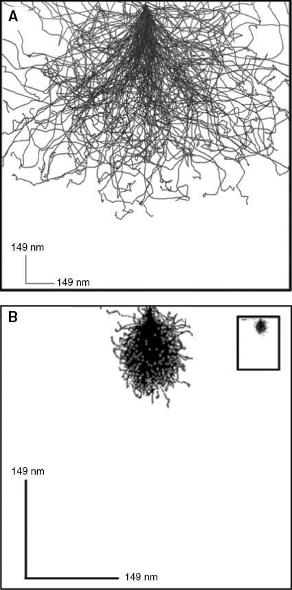
Comparison of the interaction volume of an electron and a helium ion interaction with a carbon surface. (A) Simulation of the interaction volume generated by a 10-kV electron beam bombarding a carbon surface generated by the Win-X-ray program (http://montecarlomodeling.mcgill.ca/software/winxray/features.html); the scattering image includes backscattering electrons. (B) Simulation of the interaction volume generated by a 10-kV helium ion beam bombarding a carbon surface generated by SRIM program.
Topological variation of a sample’s surface, such as the alteration to the surface roughness or the presences of high aspect ratios of surface features will alter image contrast. Another topological consideration important for image/contrast formation is shadowing, in which a surface structure blocks a portion of the sample from the ion beam. This is particularly true when imaging nanoscale topologies that are composed of nonconductive materials (as most polymeric materials where the accumulated surface charge cannot escape). Moreover, the larger interaction volume of an electron beam may completely encompass a nanoscale structure being observed creating additional resolution problems for SEM imaging of nanostructures polymeric material. In traditional SEM, the issues in imaging nonconductive biological and polymeric samples have been mediated somewhat by lowering the beam energy [29, 30]. Helium ions having more localized interactions with surface materials, have an inherent reduction in some of the potentially confounding effects observed in SEM when imaging nanostructured features with high aspect ratios, even those composed of nonconductive material [18, 20]. Furthermore, when imaging thin materials with HIM, interactions within the sample material are able to generate ion-induced SE from adjacent objects, which can be useful in fields ranging from materials science to biological sciences [18, 31].
Structural variance within a chemically homogenous sample, itself, also affects contrast formation with HIM. It may be possible to characterize the crystalline properties of polymers using ion channeling in HIM. Ion channeling is the phenomena in which an ion beam differentially interacts with a crystalline lattice of a material in an angle-dependent manner and is used as the basis of analytical techniques such as Rutherford backscattering [32–34]. Although the operating energies of the helium ion beam in HIM is significantly lower than in techniques such as Rutherford backscattering, HIM has been used to characterize a polycrystalline gold film and describe orientation-dependent contrast formation [33].
3 High-resolution imaging of polymer nanostructures
3.1 Polymer-based composites
Composite materials dominate the modern material world and are extremely important from both scientific and technological viewpoints. Polymer-based composites are widely used in construction, transportation, and aerospace industries. Many of such materials have been designed and tested to have a unique set of properties required for some niche applications. Very often, a synergistic effect can be achieved when the properties of the composite are significantly exceeding the additive sum of those of the constituting components thus offering superior mechanical, thermal, or degradation-resistance properties. In polymer-based nanocomposites, mechanical flexibility and processibility of a polymer (which is used as a continuous phase or matrix) can be combined with unique properties of a nanostructured filler (such as high electrical conductivity, magnetic properties, dielectric constant, etc.). The filler may be of inorganic or polymer nature and can be of an isotropic (nanoparticles), anisotropic (nanowires, nanofibers, nanotubes), or hierarchical (dendrimers) shape. The nanofiller can be synthesized in situ in functional polymer matrix or can be dispersed in it during fabrication protocols (solution or melt mixing) [35].
Carbon nanotubes (CNTs) have been introduced more than two decades ago and possess unique mechanical, electrical, and thermal conductivity properties, which makes them very attractive as a filler material for developing conducting polymer composites for modern engineering applications. The high aspect ratio of the CNTs significantly lowers their electrical conductivity percolation threshold compared to the conventional polymer/carbon black composites. Therefore, polymer/CNT composites have been suggested for many high tech applications including RF interference shielding coatings, memory devices, field effect transistors, and ultrasensitive physical, chemical, and biological sensors [36].
Aggregation of nanoparticles or nanotubes in the polymer matrix represents one of the major problems in the creation of polymer nanocomposites. CNTs have a natural trend for the formation of bundles – thicker fibers constituted with seven or more individual nanotubes, thus, significantly constraining the final characteristics of the material. Therefore, both new technological solutions for CNTs dispersion and nondestructive methods of their structural control are required. Figure 3A,B demonstrates CNT bundles as viewed by HIM and by AFM techniques. Visible lateral cross-sectional dimensions of thread-like features in AFM topography image (Figure 1B) are exaggerated due to the effect of AFM tip shape convolution with cylindrical features attached to a flat substrate (silicon wafer surface). The real diameter of the features can be extracted from the height distribution analysis (inset) and gives an evidence that they are aggregates (bundles of 10–30 nm diameter) constituted with seven or more individual single-walled carbon nanotubes of 1.3 nm diameter [37]. HIM image of the same nanotubes (Figure 3A) explicitly shows these aggregated structures and reveals the details of the bundle formation. Moreover, self-suspended nanotubes without substrate can be imaged. The bottom portion of Figure 3 shows comparison between imaging capabilities of the ultrasonic mode of scanning probe microscopy (so-called ultrasonic force microscopy (UFM)) and HIM in visualization of nanotubes hidden underneath a polymer composite surface. As demonstrated [38], polyurethane (PU) can be used as a flexible matrix promoting fine dispersion of the nanotubes. Figure 3D has an enhanced contrast associated with the difference of interaction of ultrasonic waves with the matrix and the filler. The PU matrix is significantly damping sound wave propagation and appears as a dark background in the image. Owing to a much higher modulus of elasticity (∼1 TPa for CNTs vs. ∼100 MPa for PU), the nanotubes appear as bright lines in UFM allowing their easy identification and mapping. HIM imaging (Figure 3C) also shows high contrast for PU-CNT systems but because of a different reason. CNTs are electrically conductive, while the matrix is a dielectric material. Charge density distribution imposed during ion beam exposure causes high contrast imaging in this case. Generally, HIM technique has an advantage of a more simple (no special sample preparation) nanometer-scale imaging of polymer-CNT composites revealing details of the nanotube dispersion and aggregation within the polymer matrix.
![Figure 3 Comparison of SPM and HIM imaging of polymer-carbon nanotube composites. (A) HIM image of a CNT bundle, (B) AFM topography image of single wall carbon nanotube bundles (constituted of seven individual nanotubes on average) on silicon wafer surface (inset shows cross-sectional scan with peak heights corresponding to nanotube bundle diameters), (C) HIM image of polymer-impregnated carbon nanotubes, (D) UFM image of CNT-polyurethane nanocomposite surface [Image 3c reproduced with permission from Carl Zeiss Microscopy, Peabody, MA, USA].](/document/doi/10.1515/ntrev-2014-0004/asset/graphic/ntrev-2014-0004_fig3.jpg)
Comparison of SPM and HIM imaging of polymer-carbon nanotube composites. (A) HIM image of a CNT bundle, (B) AFM topography image of single wall carbon nanotube bundles (constituted of seven individual nanotubes on average) on silicon wafer surface (inset shows cross-sectional scan with peak heights corresponding to nanotube bundle diameters), (C) HIM image of polymer-impregnated carbon nanotubes, (D) UFM image of CNT-polyurethane nanocomposite surface [Image 3c reproduced with permission from Carl Zeiss Microscopy, Peabody, MA, USA].
3.2 Polymer nanoparticles and nanofibers
As has been mentioned already, polymers are “natural” nanomaterials due to the fact that common macromolecular dimensions fall in the range of a few to several tens of nanometers. Some methods of polymer synthesis (emulsion and suspension polymerizations) or physical techniques (self-assembly, Langmuir-Blodgett, layer-by-layer deposition) can be used for shaping of polymer chains in nanoscale objects like nanoparticles, nanofibers, or ultrathin films. A typical example of such processes is polymer latexes. Polymer colloids or latexes are common for application ranging from cosmetics and pharmaceuticals to adhesives and coating [39]. Latexes have typical diameters in the range of a few hundreds of nanometers, and therefore, the entire surface created by a few grams of such polymer may be of the order of 100 m2. As a result, physical properties of latex suspensions such as their stability are almost fully determined by their surface properties. Latex suspensions are therefore good model systems for the study of surface-related problems (so-called “soft condensed matter”) [40–42]. Polymer colloidal particles can be also used as “building blocks” for construction of larger mesoscale structures. After the formation of the final film or coating, the individual particle identity is vanished to produce a homogeneous material [43]. A key advantage of such approach is that it offers fine control of the final structure at different levels from the nanoscale (within particles) to meso- and even macroscale through the creation of ordered assemblies [8].
Even more sophisticated structures can be created with core-shell nanoparticles enabling inherent molecular level compatibility of the components and otherwise mutually exclusive properties (e.g., electrically conductive shell on insulating core) [44–46]. This approach has found widespread attention especially recently in connection with development of printed electronics and 3D printing technologies [47–50]. Application of core-shell polymer nanoparticles for creation of highly porous functional materials suitable for chemical sensor applications and their characterization with HIM was demonstrated earlier [51]. Functional sensing shell has been prepared from intrinsically conductive polymer polyaniline (PANI) whose conductivity depends on the environment. Moreover, the shell could be structured at the nanoscale through application of special polymerization approaches [52–54]. Simultaneously, relatively bulky core possessed mechanical stability and was used as a solid frame for the final sensing material.
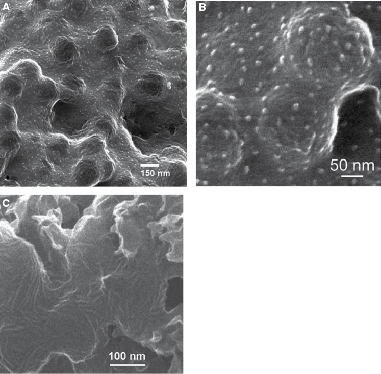
The core can introduce special functions in the system. For instance, a core-shell nanoparticle can introduce desirable physical properties like macroscopic polarization, optical transparency, mechanical toughness, and thermal processability. The nanoscale functional shell can be formed on top of relatively large (micrometer-sized) cores. As pointed out in [55] the core-shell synthetic approach enables reduction of human health and environmental risks associated with formation of aero-sols in existing nanofabrication protocols. The authors introduced the way of creation of nanostructured electrically conductive composites based on submicron core-shell particles with poly(vinylidene fluoride) core and PANI shell. The PANI component could be additionally doped with various dopants, thus, broadening the spectrum of possible functionalities. PVDF offers good processability, chemical inertness against many organic solvents, acids, and bases, and thermal stability [56]. The morphology and electrical properties for the PVDF-PANI core-shell system were studied with HIM depending on the preparation conditions (Figure 2). The possibility of preparing stable and mechanically strong PVDF/PANI (DBSA) films with excellent sensing properties has been demonstrated. HIM studies have revealed that application of short-time annealing, above the melting point of the PVDF matrix, made possible additional adjustment of the structure and conductivity properties of the material. Image A in Figure 4 shows as-prepared core-shell particles. The particles are characterized with a smooth surface and narrow size distribution. The electrical contact between conductive PANI shells is not perfect, and therefore, the deposited film still possesses insulating properties. When annealed at 180°C for a short time (Figure 4B), simultaneous softening of the PVDF core and welding of the shells leads to formation of a porous monolithic film and an electrically percolation system achieved with a relatively small (∼20%) volume fraction of the conductive component. The resulting nanoporous films consisting of tightly bound PVDF/PANI(DBSA) core-shell submicron particles with PANI shells of up to 10 nm thickness exhibited high sensitivity to gaseous ammonia with a ppb range detection limit. Interestingly, due to an incomplete doping of the polymer chains, the nanocomposite material was also sensitive to gaseous HCl, however, in a narrower concentration range.
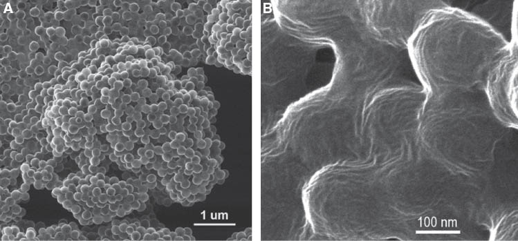
HIM imaging of PVDF-PANI core-shell nanoparticles. (A) nanoparticle aggregates formed after casting from chloroform dispersion; (B) porous monolithic film formed after short term annealing of the solution cast film at 180°C (above the melting transition temperature of the PVDF core).
Polymer nanofibers are another example of nanostructured polymer materials. They can be produced via electrospinning protocols [57, 58] or, in some cases, just due to spontaneous self-assembly process [16]. Figure 5 demonstrates high applicability of HIM in direct imaging of polymer nanofibers. The left image (A) shows an electro-span poly(lactic acid) nanofiber. This polymer is an example of a biodegradable, thermoplastic, aliphatic polyester derived from renewable resources [59–63]. Several distinct forms of polylactide exist due to the chiral nature of the lactic acid. Poly-l-lactide (PLLA) is characterized with a moderate degree of crystallinity (∼37%), has Tg between 50°C and 80°C, and a Tm between 173°C and 178°C. PLLA is currently used in a number of biomedical applications and is also evaluated as a material for tissue engineering (scaffolds). Image A shows the onset of formation of mineral particles of the surface of the fibers (mineralization process). Nucleation of inorganic phase and development of mineralization can be studied with nanoscale resolution with HIM without special sample preparation requirements. A characteristic waviness of the fibers, which is a result of flow instabilities during electrospinning process, can be also observed and characterized in detail. The observed nanoscale roughness of the PLLA fibers helps in creation of tight attachment of the inorganic phase to polymer nanofiber frame. The right image (B) shows polyaniline (PANI) nanofiber spontaneously formed due to self-organization process during polymer synthesis [51]. Nanostructuring of PANI as a conductive polymer with environmentally dependable conductivity allowed the fabrication of a supersensitivity to ammonia vapor chemical sensors through simple conductometric transducer scheme [51]. Electron microscopy and diffraction have confirmed a high degree of orientation of PANI molecules within the fibers, which is in tune with the observed molecular level smoothness of their surface. The image shows that the PANI nanofiber and supporting polished silicon wafer surface have similar roughness (i.e., on a level of 0.4 nm). In both examples of Figure 5, the details of the surface roughness and texturing on the fibers could be revealed only due to the application of HIM technique. These details are lost in AFM imaging because of high local curvature of the surface (small radius of fibers) and difficulties of their tight attachment to a substrate required for high-resolution scanning. SEM imaging does not offer high resolution due to significant surface charging of insulating polymer materials. TEM does offer atomic resolution imaging and chain orientation, however, only with a complex sample preparation procedure. The surface topography details are typically lost in TEM images due to relatively low contribution from the surface to the image contrast in comparison to the “bulk fiber” electron scattering.
![Figure 5 HIM imaging of polymer nanofibers: (A) electrospan PLLA nanofibers used as a scaffold (mineralization process can be seen on the surface); (B) self-organized fibers of polyaniline polymer. Insets show higher magnification images [Reproduced with permission from Carl Zeiss Microscopy, Peabody, MA, USA].](/document/doi/10.1515/ntrev-2014-0004/asset/graphic/ntrev-2014-0004_fig5.jpg)
HIM imaging of polymer nanofibers: (A) electrospan PLLA nanofibers used as a scaffold (mineralization process can be seen on the surface); (B) self-organized fibers of polyaniline polymer. Insets show higher magnification images [Reproduced with permission from Carl Zeiss Microscopy, Peabody, MA, USA].
3.3 Nanoporous polymer systems
Nanoporous polymer beads represent another challenging system for microscopy studies. Porous polymer resins are prospective materials for hydrogen storage, as a sorption media as well as for sensor applications. In the latter case, a porous polymer membrane or porous beads of desirable size and high specific surface area should be functionalized to enable selective binding of targeting molecules or atoms on their surface. The adsorption of the analyte species on the surface can be then monitored either directly by detection of emitted light intensity (if the analyte molecules have fluorescence centers) or indirectly via incorporation of specially designed fluor molecules to convert radiation (X-rays, γ-rays, electrons, α-particles, or neutrons) into energy of light. Recent reviews demonstrated several successful approaches for synthesis of porous polymer particles [64, 65]. The porosity of the fabricated beads can be controlled by the type and concentration of a porogen and the degree of polymer matrix crosslinking. In our recent study, we have applied three different porogens in order to achieve a significant variation of the nanopore distribution within the same polystyrene (PS) matrix during suspension polymerization fabrication protocol.
Pore structure characterization of polymer beads is not a trivial task. The pore size distribution analysis of polymer materials can be accomplished by surface porosimetry techniques and modeling sorption-desorption curves via application of some of theoretically developed approaches [66]. This indirect analytical technique is generally accepted and gives reliable data. Alternatively, the same data can be also be extracted from small-angle X-ray or neutron scattering techniques [67, 68]. However, the direct visualization of the pore structure with pore size ∼2 nm or smaller has not been possible until recently due to technical limitations of traditional microscopy techniques (TEM, SEM, AFM). In our study, we compare the morphological features and porosity of polystyrene-based polymer resins prepared using suspension polymerization technique with the application of three different porogens resulting in three different types of porous structures. The direct nanoscale resolution imaging of PS beads surface was possible only with the application of HIM (Figure 6). Figure 6 shows comparative study of PS beads prepared with three different porogens. The left images are low-magnification pictures showing the overall quality of the beads and their surface roughness. One can see similar smooth surfaces for the samples prepared with toluene and n-heptane porogens, while the addition of a nonionic span-80 surfactant (water in oil in water, w/o/w, or double emulsion approach) introduces highly developed surface to the system. Some additional contrast associated with surface charging (the beads are studied in their native state) during imaging is clearly observed but does not affect the quality of the images. Similar pictures obtained with SEM are reported in many related publications but require thermally evaporated metallic layer on the bead surface. The evaporated metallic layer masks the intimate details on the surface and limits the resolution of SEM technique to 20–50 nm (the typical size of metallic film domains). On the contrary, high-resolution imaging of pores is still possible with HIM technique. On the right images of Figure 6, the nanometer scale details of the bead surface are clearly visible. The contrast arises from the different secondary electron emissions from the top surface and the surface of the caves (pores). Comparison of the size and distribution of dark spots representing pores show that toluene porogen promotes formation of the smallest pores (average size 2–3 nm), followed by n-heptane porogen (∼5–10 nm pore size), and by span-80 (w/o/w) system with a very broad pore size distribution (30–50 nm).
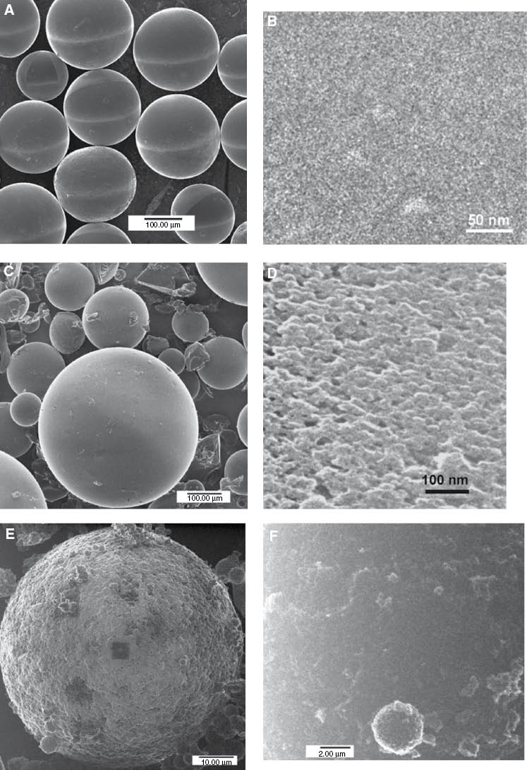
HIM images of nanoporous polystyrene beads prepared via suspension polymerization with three different porogens: toluene (A, B), n-heptane (C, D), and Span-80 (E, F) (see explanation in the text). Low-resolution images (left) give insight in the bead’s size distribution and surface roughness, while high-resolution images (right) allow visualization and direct measurements of the pore size and pore size distribution not available in other microscopy techniques.
3.4 Surface crystallization in ultrathin polymer films
The ability of long polymer chains to form ordered structures during the crystallization process is one of the most striking phenomena in condensed matter physics [69]. The phenomenon has been studied since the origin of polymer science both by the real space imaging methods (TEM, SEM, AFM, etc.) and diffraction techniques (electron diffraction, wide angle X-ray diffraction, small-angle X-ray scattering, reflection high-energy electron diffraction, etc.) The real space imaging methods are usually applied to probe morphology, crystallization kinetics, and melting behavior, while the diffraction techniques can detect the crystalline lattice, lamellar orientation, crystallinity, and transition temperatures [70].
The most common morphological superstructures spontaneously formed during polymer crystallization from melt are spherulites, which are polycrystalline and semicrystalline in nature. Formation of polymer single crystals can be observed when crystallization happens from dilute solutions. This leads to formation of platelet shape single crystals (lamellar) first reported with TEM technique in the later 1950s [71–73]. The lamellar single crystals have one dimension (thickness) in the range of several or tens of nanometers and lateral dimensions of a few micrometers and represent the basic unit of crystalline polymers, of which spherulites and other polycrystalline aggregate are composed.
Especially interesting is the investigation of the crystallization phenomenon in thin polymer films with the thickness comparable with the radius of gyration of polymer chains. Owing to geometrical confinement, such polymer materials possess structural organization and physical properties different from the bulk state [74–76]. Thin polymer films and coatings constitute an essential portion of modern organic materials and find applications in many branches of industry including packaging, printing technology, and plastic electronics. Not surprisingly, structural organization and crystallization phenomenon of polymer materials in ultrathin films has been a focus of several recent research efforts [74–76]. The variety of crystallization protocols reported in literature for thin polymer films depending on the film thickness can be reduced to three characteristic types: i) spherulitic (or bulk-like crystallization observed in relatively thick films with the thickness, d, much higher than the radius of gyration of the polymer chains Rg); ii) dendritic crystallization for d∼Rg; and iii) quasi-two-dimensional crystallization in the case of highly confined films (d<Rg) [77–82]. In the latter case, the crystallization process can be significantly modified by a process of polymer layer dewetting from the solid surface (in case of weak polymer-substrate interaction) or can be suppressed (in case of strong polymer-substrate interaction) [83–85].
Generally, crystallization in very thin films comparable to the Rg can be described as diffusion-limited crystallization (DLC) [77–82, 86]. This term should be understood both in the sense of limitations in chain mobility, which is increasing with temperature, and in terms of limited amount of polymer material (just a few polymer chains across the film thickness) capable for rearrangement necessary for the crystalline phase formation. The first limitation can be referred to as a kinetic constrain, while the second one is a geometrical constrain (i.e., can be treated as temperature-independent parameter). As demonstrated by several publications, both glass-transition and crystallization transition points (Tg and Tc) will be affected by the film thickness and vicinity of the solid surface [87–91]. This is due to enhanced mobility of the surface layer in comparison to the bulk material (relative contribution from the surface property will increase as the film thickness is reduced).
Morphological features of crystallization in thin polymer films have been intensively studied during the last decade [70]. Despite a number of publications on surface crystallization of various polymer systems, the real understanding of the physical process is still to be achieved. Therefore, a systematic study of the crystallization process and the final crystalline morphology for well-characterized set of polymers with application of high-resolution microscopy techniques like AFM or HIM allowing in situ characterization is highly desirable.
Polyesters constitute the main segment of polymer materials prospective for printed electronics and packaging applications. They can be used as a flexible substrate to support electronic devices, as dielectric interlayers as well as in the top encapsulating coating. Poly(ethylene terephthalate) (PET) is a one of the most common thermoplastic polymers from the polyester family. It is widely used in synthetic fibers; packaging (beverage, food, and other liquid containers) engineering and thermoforming applications [92]. Poly(ethylene 2,6-naphthalate) (PEN) is similar to PET but has higher glass and melting transition temperatures, which makes it attractive for medical (hot steam sterilization, etc.), mechanical, and chemical applications (due to its mechanical stability and chemical inertness). In our study, ultrathin PET and PEN films were prepared from polymer solutions via spin- or dip-coating procedures, which suppressed the crystallization process during polymer film fabrication. Subsequent in situ annealing of the samples at various temperatures allowed monitoring of the diffusion-limited cold crystallization process by AFM [93].
The general scheme of formation of surface crystals in thin polymer films is presented in Figure 7A. Formation of surface crystals with a special dendritic morphology is observed for ultrathin films with the thickness comparable with the radius of gyration of polymer chains. Based on our AFM studies, a phase diagram of diffusion-limited crystallization behavior (in temperature-film thickness coordinates) was constructed [93]. Existence of three characteristic layers (as shown in Figure 7A) determines the features of crystallization behavior in thin films of crystallizable polymers [13, 93]. Figure 7 shows typical surface crystal morphology as observed by AFM in comparison with HIM imaging. AFM as height distribution-sensitive technique allows better contrast in comparison to HIM imaging. Figure 7B demonstrates a dendritic PET crystal grown on top of an amorphous PET “background” film. The total PET film thickness is quite low (40 nm). The main features of the crystalline structure can be recognized. Also, application of a stop-and-go approach (i.e., repetition of annealing and AFM imaging events) of direct in situ annealing will permit characterization of the kinetics of the crystallization process. While the vertical resolution of such imaging is in a subnanometer level, the lateral resolution is limited by AFM tip-surface feature shape convolution and depends on the tip sharpness. In the best case scenario, the details of the crystalline structure smaller than 10 nm cannot be resolved. HIM technique does not suffer this limitation making it perhaps better suited for this type of characterization. Figure 7C demonstrates that crystalline beams of the dendritic structures are actually constituted with smaller crystalline domains (5–20 nm lateral dimensions).
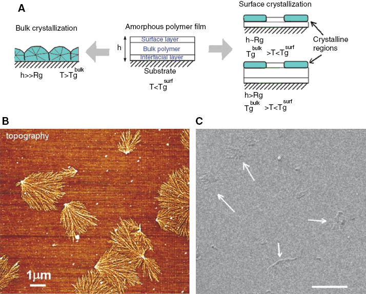
(A) Bulk vs. surface crystallization phenomena in a crystallizable polymer film under condition of geometrical confinement (film thickness is below 200 nm and comparable with the characteristic size of polymer chains –the radius of gyration); (B) AFM image of PET dendritic crystals grown on the surface of otherwise amorphous film (40 nm thickness); (C) the same structure visualized by HIM (200 nm film thickness). Arrows point several dendritic PET crystals. Scale bar 1 μm.
Application of micro-imprinting protocols allowed the fabrication of polymer films with 2D (lines) and 3D (dots) type of geometrical confinement. Figure 8 shows examples of AFM and HIM imaging of such structures. The HIM technique has a higher applicability to study of the nano-imprinted structures as it does not have the same problems of high roughness or high surface curvature that limits the application of the AFM technique. In Figure 8A,B, the details of the surface roughness are lost, and information about surface topography between imprinted features is unavailable. On the contrary, HIM images (Figure 8C–H) show the real structure with vertical side walls of the imprinted features (dots or parallel lines). One can see that annealing of the structures causes partial dewetting of the PET film in the case of the dotted pattern, but no surface crystallization process is observed. Therefore, AFM and HIM post investigation of the imprinted film morphology depending on the annealing temperature revealed a remarkable stability of the amorphous phase. Compared to 1D-confined films (Figure 7), where characteristic surface crystallization was observed at T<Tg, no sign of surface crystallization process was observed even at temperatures exceeding the bulk melting transition. Further studies of the surface crystallization in PET and other crystallizable polymers are in progress.
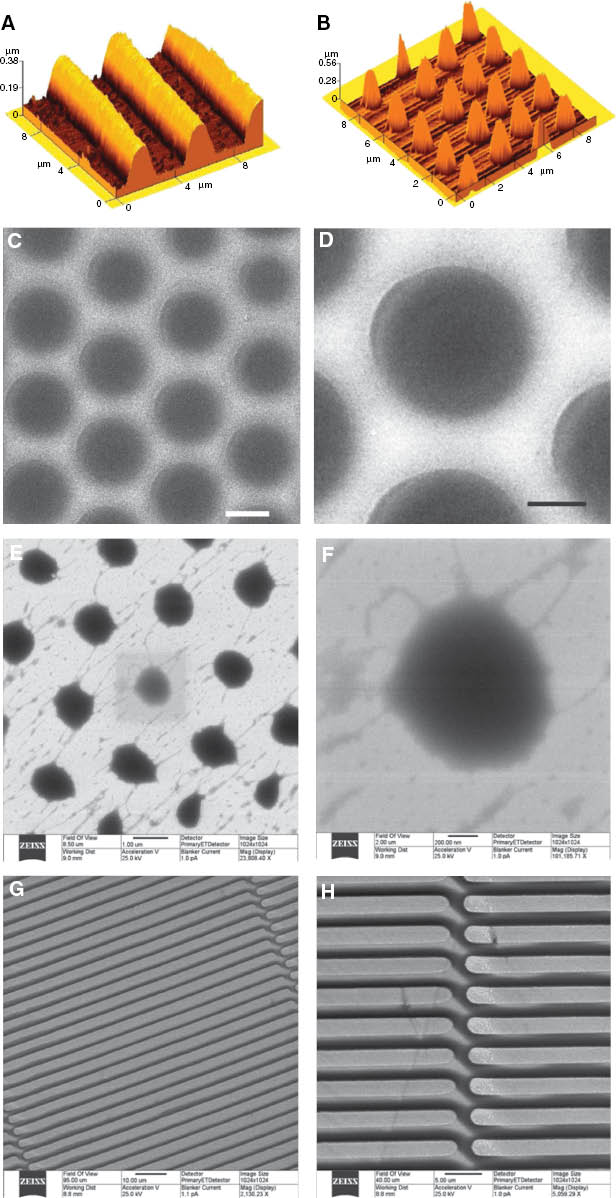
AFM (A, B) and HIM (C–H) images of PET imprinted films with 2D (lines) or 3D (dots) type of geometrical confinement. (C) and (D) portions are different magnification HIM images of an as-prepared film PET film; (E) and (F) show the morphology of the same film after its annealing at temperature 5° above the Tm of PET; (G) and (H) show different magnification HIM images of a PET film with imprinted parallel lines (no sign of surface crystallization can be seen before or after annealing). AFM images do not allow high-resolution characterization of the film surface (especially) between the nano-imprinted features due to high local curvature and surface roughness of the surface.
3.5 Polymer-based devices
3.5.1 Bulk-heterojunction solar cells
Organic photovoltaic (PV) devices are considered the third generation of PV technologies following first-generation, single-junction crystalline silicon cells and second-generation, thin-film solar cells based on CdSe, copper indium gallium diselenide (CIGS), and a-Si or nano-Si [94–96]. Recent advances in solution-processable organic and inorganic semiconductors, as well as their composites, have led to the possibility of using significantly lower cost manufacturing methods, such as printing and coating, and simplify the fabrication of PV devices. One of the best candidate for low-cost manufacturing PV devices is polymer-based bulk heterojunction (BHJ) solar cells. The setup of such devices is based on a mixture of electron donor and electron acceptor materials that are sandwiched between two selective electrodes. The two intermixed photoactive materials create an active layer of the cell. Its nanoscale, heterophase character enables a very efficient charge generation throughout the bulk [97]. The morphology of BHJ cells has to be controlled at the nanoscale to achieve efficient light energy harvesting via exciton diffusion and dissociation phenomena. Polymer BHJ solar cells showed a remarkable progress during the last 3 years with the efficiency exceeding 10% for the best devices [98–101].
Probably, the most studied active materials for this type of solar cells are conjugated polymers, such as P3HT (poly-3-hexylthiophene) or other polythiophene derivatives (especially donor-acceptor type) in combination with the fullerene-based acceptor material [91, 98–101]. Such polymer solar cell can be deposited via solution-based protocols (wet deposition) or vacuum evaporation techniques on top of a transparent substrate (glass or PET) coated with a thin layer of an optically transparent electrically conductive materials (indium tin oxide – ITO) [102, 103].
Nanostructured organization of the BHJ layer is critical and can promote exciton drift to the donor-acceptor interface in cases where the components of the active layer form interdigitated structures (with dramatically enhanced specific interfacial area). These structures can be created deliberately via control of the crystalline morphology of polymer photoconductor and the degree of phase separation in the system (a proper choice of the components, and special thermal annealing protocols) [104–106]. The same structures also can be created via addition of small quantities of special molecular compatibilizers (amphiphilic or bi-anchor thiols) [106]. Ordinary (random) BHJ structure is then created spontaneously within the active layer due to phase separation of the components under thermal annealing (120–150°C). The length of the exciton diffusion puts strict requirements on the size of the polymer phase domains, not to exceed 20 nm. Other morphological restrictions include desirable alignment of the polymer chains (to promote high mobility of charge carriers) and their orientation normal to the electrode surface (this allows higher active layer thickness – i.e., higher light energy absorption with simultaneously reasonable electrical resistance). Further enhancement of the PV efficiency could be achieved if so-called organized heterojunction structure is created [107]. Such a special morphology offers multiple exciton dissociation sites and separate charge pathways, thus limiting exciton recombination. As a result, thicker and therefore more absorbing polymer films can be used as an active layer.
AFM and electron microscopy techniques were applied successfully to study the morophology of the active layer components depending on their ratio and annealing procedures [108]. Particularly, the size and orientation of polythiophene (PT) nanocrystals is responsible for BHJ cell performance due to anisotropy of charge carrier mobility along and across the polymer chains [109]. Nanometer resolution imaging of organic BHJ is a challenging goal; however, such information may assist in the development of PV devices with improved efficiency. TEM as the highest-resolution electron microscopy technique was applied to determine the nanoscale structures present in thin BHJ films (<100 nm) [110, 111]; however, such images represent a projection of structures detected through the sample thickness [112]. Unambiguous interpretation of the bright-field TEM data was difficult due to small contrast variation within the polymer layer and possible artifacts arising from thickness variation and electron beam defocusing [111, 113, 114]. Moreover, most of the PV cell organic materials showed very low stability under the electron beam exposure. To reduce the beam damage, energy filtered transmission electron microscopy (EFTEM) has been used to image P3HT/PCBM thin films [113]. The authors applied computer-aided reconstruction based on the TEM images, which has proved an existence of a three-dimensional network of P3HT nanofibers within the active layer; however, the size and distribution of the polymer domains obtained from bright-field and energy-filtered images reconstruction techniques were not consistent.
Application of HIM technique in this case has an advantage of finely focused and less destructive ion beam enabling visualization of the nanoscale compositional variation in a PV device. The components of the BHJ system show different brightness in their secondary electron (SE) emission, which depends on the ratio of π-bonds to the sum of π- and σ-bonds in an organic molecule [115]. As a result, the P3HT component appears brighter than PCBM in HIM images (Figure 9). Monitoring of a gray level distribution of the HIM images taken across the sample allowed high-resolution mapping of the BHJ layer components. Particularly, it was determined that PCBM domains are slightly elongated in shape and have their dimensions below 20 nm (∼12 nm in length), which is consistent with the observed efficient exciton dissociation in the system. Therefore, HIM was proved as a powerful method enabling ex situ (or even in situ) characterization of organic semiconductor thin films and devices [116].
![Figure 9 HIM imaging of BHJ solar cell active layer constituted with P3HT electron donor and PCBM electron acceptor. High-resolution imaging and high contrast are observed because of different secondary electron yield properties of the components [Reprinted with permission from (A.J. Pearson, S.A. Boden, D.M. Bagnall, D.G. Lidzey, and C. Rodenburg, Imaging the Bulk Nanoscale Morphology of Organic Solar Cell Blends Using Helium Ion Microscopy, Nano Lett, 2011, 11(10): p. 4275–4281). Copyright (2011) American Chemical Society].](/document/doi/10.1515/ntrev-2014-0004/asset/graphic/ntrev-2014-0004_fig9.jpg)
HIM imaging of BHJ solar cell active layer constituted with P3HT electron donor and PCBM electron acceptor. High-resolution imaging and high contrast are observed because of different secondary electron yield properties of the components [Reprinted with permission from (A.J. Pearson, S.A. Boden, D.M. Bagnall, D.G. Lidzey, and C. Rodenburg, Imaging the Bulk Nanoscale Morphology of Organic Solar Cell Blends Using Helium Ion Microscopy, Nano Lett, 2011, 11(10): p. 4275–4281). Copyright (2011) American Chemical Society].
3.5.2 Polymer-based sensors
Intrinsically conducting polymers (ICP) such as polyaniline, polythiophene, and some other polymers have a proven record of their application as chemical sensor materials. These polymers have a quite high sensitivity, are relatively simple to synthesize, lightweight, and can detect gases at ambient temperature [35, 43–45, 47, 48, 117–121]. PANI differs from other ICP due to its higher stability and much lower cost. Moreover, the electrical conductivity of this polymer can be reversibly controlled in two different ways: either by electrochemical or chemical oxidation/reduction processes or by protonation/deprotonation in a simple acid-base chemical interaction. Additionally, PANI can be combined with some thermoplastic polymers to form a composite with a very low percolation threshold of conductivity. The resulting composites may effectively combine mechanical properties of the thermoplastic polymer matrix and the electronic properties of PANI to efficiently serve as an active component of an organic gas sensor device [122, 123]. Nanostructured PANI-based materials fabricated as nanofibers, core-shell particles, or nanotubes are attractive due to their ability to form thin conductive films with a porous structure [124, 125]. The latter morphology enables easy penetration of the analyte molecules inside the sensor film dramatically increasing the detection limit and sensitivity while simultaneously reducing the response time of corresponding sensor devices [126, 127].
Several recent publications show potential of nanostructured PANI-based composites as sensing materials for ammonia gas with the detection limit in a ppm range [128, 129] Application of HIM microscopy technique allowed monitoring and optimization of the morphology and porous structure of PANI-PVDF core-shell-based films during their fabrication [55, 130]. Moreover, sensitivity of the HIM contrast formation mechanism to a charge state of the material under study allowed better understanding of the physical sensing mechanism during sensor material operation. Figure 10 shows the optimized nanoporous polymer film with high sensitivity to ammonia and an example of irreversible transformation of the PANI layer due to chemical interaction of a dopant with HCl analyte. The latter process leads to formation of nanoscale dots of dopant salt clearly visible in HIM because of their higher electrical conductivity in comparison to a semiconductor PANI film.
HIM imaging of polymer-based sensor devices; (A, B) active layer of PVDF-PANI ppb range ammonia sensor layer exposed to ammonia for a long time (phase separation and formation of dopant-ammonia salt is observed), (C) nanoporous sensor film based on PVDF-polythiophene core-shell nanoparticles after elevated temperature sintering of the particles. Polythiophene shows high sensitivity to volatile organic solvents such as acetone, chloroform, toluene, and some others.
Figure 10C shows another example of nanostructured semiconducting polymer polythiophene (PT) prepared through the same approach – i.e., first, core-shell nanoparticles with a PVDF core and PT shell were synthesized, and then, particulate films were cast from a chloroform dispersion and sintered into a solid nanoporous film under short-term thermal treatment [130]. Nanostructured PT materials possess a ppm detection limit and sensor discrimination capability in detection of volatile organic compounds (VOCs) such as acetone, chloroform, toluene, and others) [131–133].
3.6 Imaging of biopolymers
Biological polymers or biopolymers are the molecules of life; they compose the bulk of the dry mass of all living organisms, they assume the bulk of metabolic and structural duties in the cell, and in the case of the nucleic acid biopolymers deoxyribonucleic acid and ribonucleic acid, these molecules function as the blueprint for life itself. The interest of the structural aspects of biopolymers has risen over the past 10 years as properties such as self-assembly and self-organization has been demonstrated for many of the biological molecule and biopolymer systems [134]. Self-assembling collagen arrays, DNA origami, and now protein origami clearly demonstrate how elaborate and complex nanostructured surfaces can be generated de novo from a relatively simple collection of biopolymers and little or no scaffolding using a bottom up strategy [134–139]. The hope is that larger-scale self-assembly of even more elaborate nanopatterned surface will be possible using similar principles and approaches.
There are three major classes of biopolymer: polysaccharides, polypeptides, and nucleic acids. Polysaccharides are found throughout the biosphere, alone and also conjugated to other biopolymers such as proteins, in the form of glycoproteins, or to lipids in the form of glycolipids [140, 141]. In comparison to nucleic acids and proteins, carbohydrates have larger capacity of complexity through the presence of numerous chiral centers within the sugar/monosacchride subunits, the greater possible combinations of glycosidic linkages between different carbons within the sugar subunits resulting in branching, and to modifications to individual sugar subunits such as acetylation, methylation, oxidation, and sulfation [139, 142]. Given this extraordinary potential diversity, the extent of structural diversity of polysaccharides is just being explored. Nucleic acids and polypeptides have been the most extensively studied, probably for the very reason that they are the most experimentally tractable using current molecular biological techniques [139]. Polypetides are polar polymers composed of amino acid subunits. The folded, tertiary structure of a given polypeptide is determined by the primary sequence of its amino acid chain; this folding reaction is a thermodynamically driven self-assembly process. In some cases, the folded polypeptide is the functional state, and it is this state that physically interacts with other polypeptides and other components of the cell, both structural and metabolic. However, most proteins have some level of posttranslational modification prior to generating a fully functional protein complex. Natural occurring polypeptides contain 20 amino acids, although recent genetic engineering of bacteria has allowed the incorporation of synthetic amino acids into a polypeptide chain and, thus, generating potentially new and novel proteins [143]. There is a great deal of diversity in protein tertiary and quaternary structure, ranging from globular to filamentous, and many of the elaborate structures arise from the assembly of large protein-based complexes. Nucleic acids are simpler in their primary structure when compared to polysaccharides or polypeptides, them being composed of a smaller number of basic subunits called nucleotides, which contain a sugar group, a phosphate group, and a nitrogenous base group. Nucleic acids have the potential like polypeptides to fold into elaborate three-dimension structures that play catalytic and structural roles in the cell.
Regarding the structural aspects of biopolymers, there are two general levels of inquiry where the bulk of progress has been made one at the molecular/atomic level and the other at the cellular level. Techniques such as X-ray crystallography and NMR have been used extensively in the field of structural biochemistry to determine the orientation, organization, and three-dimensional structures of many biological molecules to atomic resolution, although lower resolution can be also be informative [144]. In most cases, solving of a crystal structure allows the placement of each atom of a single biological polymer, and in some cases, the organization of individual clusters of interacting biological polymers with respect to one another. However, challenges exist. X-ray crystallography requires that the protein or other biological molecule be sufficiently pure to grow the crystal to be used in the structural solution. This has been notoriously difficult for extremely large proteins or transmembrane proteins [144, 145]. Current NMR techniques require the protein or other biological molecule to be small and soluble [146]. The other level of inquiry regarding biological structure is at the cellular level. At this level, optical microscopy, especially the recent advances in confocal microscopy and super resolution microscopy have allowed unprecedented resolution of the overall organization and structure of the cell [147, 148]. While each of these approaches is important and will be important for the nanoscientist, the focus of nanobiology and nanobiotechnology falls somewhere between the cell biological view and the atomic/molecular structural view and provides a conceptual as well as technical link between these two realms.
The study of biopolymers, their structure and assembly and organization into higher-ordered structures, is a major thrust of nanoscience, and the imaging demands fall squarely between the ultrahigh-resolution techniques (such as X-ray crystallography and NMR) and the lower-resolution optical microscopy techniques; this is a zone, which the HIM is well suited. Regardless of the nature of the biopolymer, all are composed primarily of nonconductive carbon, which limits the resolution of any particle beam microscope and pose similar issues as with the imaging of other organic polymers described in the sections above; to complicate matters, many, if not most, of the biological molecules even when purified are far more complex in both structure and content. Because of these complications, imagining biological samples, i.e., molecules in situ, in the context of a cell or a tissue requires special preparations such as labeling samples with heavy metal stains to generate contrast in the material and also coating samples with nanoscale layers of gold or other heavy metals. Recent advances in the imaging of biological samples by environmental SEM or ESEM, which operates through the use of varying the pressure and/or reducing of the operating voltage of the electron beam have permitted the examination of native biological structures [149, 150]. While such techniques have enabled the imaging of uncoated biological samples, the application of ESEM typically results is a slight loss of resolution. Helium ion microscopy by virtue of the parameters described in the section of this review above, such as the lower penetration of the surface by the helium ion allows for higher resolution with a lower energy beam and the proportionally larger numbers of secondary electrons. This has led to spectacular images of biological samples such as butterfly scales, the surface cuticle of Drosophila, and even bone [31, 151, 152]. HIM microscopy demonstrates clear advantages by generating imaging with increased resolution, clarity, and increased depth of field; however, the idea that HIM imaging is simply a high-powered SEM is wrong. The role that HIM imaging in the biological sciences, especially for the visualization of the structure and organization of biological molecules is just being tapped. For instance, chitin is a crystalline polysaccharide polymer of N-acetyl glucosamine and is the primary component of the natural composite material of insect cuticles. The insect cuticle contains an elaborate and diverse set of structures (Figure 11A) and as a material displays an enormous range of physical properties, which is dependent on the organization of chitin by specific proteins in the cuticle [153]; HIM imaging of purified chitin reveals a complex network of nanoscale pores (Figure 11B).
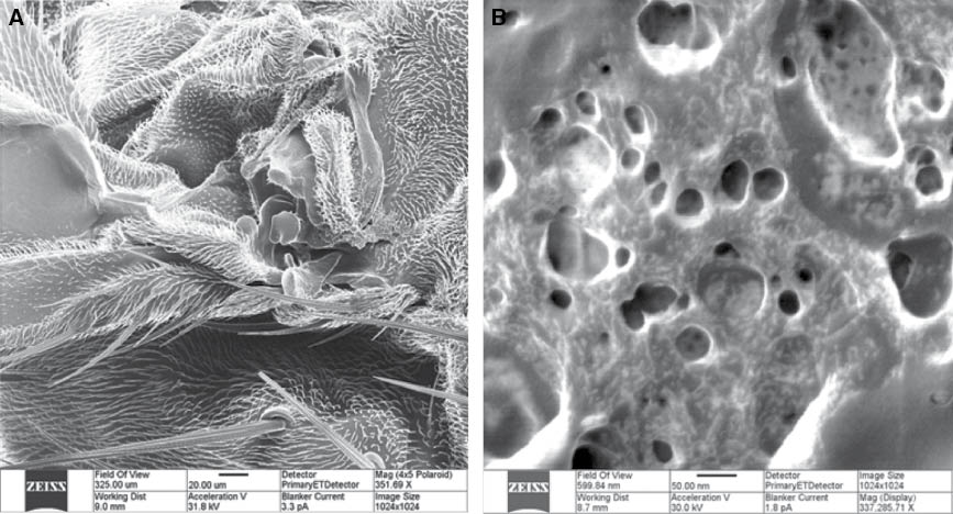
(A) HIM images of the native cuticle of Drosophila melanogaster demonstrating the elaboration of chitin polymer-based structures and sensory organs. (B) Ultrahigh-resolution image of purified chitin. Note the presences of nanoscale holes and pores.
4 HIM as a fabrication tool
In the fields of fabrication and lithography, HIM offers many advantages over traditional particle beam methods like focused ion beam (FIB) milling with gallium ions and scanning electron microscopy (SEM).
4.1 Milling/patterning
HIM combines the advantages gained from a small beam size and high brightness, along with the increased particle momentum and SE yield, to fabricate features with a high level of control. Ion milling is a standard fabrication method that involves the removal of the substrate with a focused ion beam. Samples milled with standard FIB using gallium (Ga) ion sources often have residual contamination introduced by Ga implantation during the milling process, which can lead to alteration of the surface chemistry. Moreover, the more massive Ga ions are harder to manipulate and control than He ions. They possess a greater momentum when compared to helium ions, which often results in unwanted sample damage especially when milling at the sub-30 nm scale [154, 155]. This side effect is not present in the HIM where sub-10 nm features can be milled with high fidelity. Recently, intricate and detailed devices have been milled with HIM lithography that match the theoretical resonance quality factor limit modeled in a coaxial plasmonic nanoresonator [156]. These structures would have been impossible with Ga FIB milling. Rudneva et al. have developed a heating stage allowing milling of nanoscale patterns in Si and Ti and demonstrated that unlike other methods, HIM milling did not affect the crystalline structure of the samples when heated to a high enough temperature, even at the edges of the mill [157].
The HIM can be used in a variety of biological applications as well. Not only is it capable of imaging uncoated biological samples at a very high resolution [31, 151, 152], but it has also been used to mill nanopores with diameters below 4 nm that are comparable to similar pores formed using TEM [158]. Further studies were performed, which related the milling depth to the ion dose for both direct and transmission milling and shed light into differences in milling parameters [159]. The milling process allows for multiple diameter sizes on one sample and only takes seconds to mill one pattern, making it an ideal method for wafer-scale production.
4.2 Lithography
All of the advantages arising from the gas field ion source with the helium beam have also made HIM a promising technique for ion lithography or the patterning of a resist material by exposure to the ion beam (Figures 12 and 13). Until recently, these types of patterns have been written using electron beam lithography (EBL), or Ga FIB; however, these techniques are limited in the resolution of features by the spot size and the interaction volume of the beam itself. Micrometer range scattering due to the small particle size of the electron beam gives a large interaction volume at the surface, while the gallium beam is good up to a certain point, but loses resolution below 30 nm because of its relatively large beam size [156].
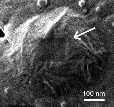
Nanolithography with HIM. 100 nm×100 nm square hole milled on top of 200 nm diameter PVDF particle.
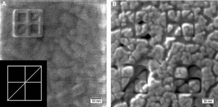
Ion lithography using the HIM. (A) Generation of nanoscale feature using He ion implantation. The surface has a 100-nm layer of gold on a Si wafer; He ion deposition occurred with 1 μs dwell time and 10 repeats of the pattern. Inset is the pattern of deposition. (B) Ion milling using HIM, a 10-nm layer of AuPd sputter coated on a Si wafer. Pattern same as in (A) with different dwell times, starting from top left and going in a z pattern: 5 μs, 10 μs, 15 μs, and 20 μs dwell times with one repeat and milling occurred.
Initially, helium ion lithography (HIL) in hydrogen silsesquioxane was shown to be capable of achieving 20 nm pitch dense structures with little resist residue, but had considerable resist residue with 10-nm pitch structures [160]. Although there were difficulties in obtaining sub-10 nm structures, the required ion dosage was shown to be approximately an order of magnitude less than that needed with EBL. The point spread function was also measured and had a reduction in the amount of micrometer range scattering similar to what is observed with electrons. Given these advantages, in its current state, HIL has feature resolution comparable to EBL, and recently, 4-nm half pitch dense patterns have subsequently been achieved using HIL [161]. These structures were subsequently used for imprint lithography on a UV curable resist, demonstrating that high-throughput single-digit nanometer fabrication of dense patterns is possible using HIL.
HIL will continue to develop and will be a major player in single-digit nanometer fabrication and lithography. The development of other ion beam milling stations using other noble gases such as neon is now being explored as a lithography tool. The neon beam allows for an increased sensitivity to resist exposure. Neon ions have been shown to be ∼10× more sensitive than He and ∼1000× more sensitive than electrons and have resolutions equal to state-of-the-art EBL [162]. It can be sure that this technology will be refined as it continues to mature and will surely have a great effect on many research areas relying on scanning particle beam lithography. While, much of HIM lithography has been concentrated on milling and processing nonpolymeric materials such as SiO2, as with other lithography methods, it is simply a matter of time until the precision of HIM lithography will be applied to polymers.
5 Conclusions and prospects
There is a growing interest in the application of HIM technique in polymer research. HIM has a unique application space defined by its applicability to high (molecular)-resolution imaging of soft materials and special mechanisms of contrast formation. The combination of ultrahigh resolving capacities, increased depth of field, and the ability to image native samples in HIM offers the possibility of polymer organization study at multiple levels from the nanoscale to the microscale. The technique is especially suitable for investigation of nanostructured polymer surfaces, polymer nanoparticles, nanofibers and nanocomposites with irregular surface features, high local curvatures, and/or high aspect ratios. Imagining such nanostructures is problematic with other modern microscopy techniques either due to special requirements for sample preparation, which disturb the natural structure of the sample (TEM, SEM) or due to inaccessibility of some portions of the material for the mechanical stylus (AFM tip).
HIM is especially suitable for studies of soft polymer and biopolymer materials. In biological system, the HIM has the potential to bridge the gap between structural biological understanding of the assembly and organization of macromolecules and the cellular roles that these molecular assemblies play in biological process such as cell adhesion, cytoskeletal dynamics, and membrane organization.
One of the most attractive features of HIM is the offered option of the FIB-based nanolithography. This gives possibility not only to study the surface of polymer materials in situ with high resolution but also enables “sculpturing of nanostructures” with the focused ion beam or with the purpose of scoping the internal portions of the material by removing its top nanolayer (milling). Application of these options to polymer studies is still in its infancy, but offers remarkable prospects (such as 3D nanoprinting) in the future.
Development of electron diffraction techniques and secondary electron energy discriminative detectors on the basis of HIM setup will broaden the spectrum of research tasks, which can be accomplished with this new type of microscopy. The former option would allow the investigation of phase-sensitive properties at nanoscale, such as phase transitions, perfectness and orientation of crystalline domains, identification of crystalline and amorphous phases, while the latter would be extremely useful for composition analysis. To realize the fullest extent and impact of this instrument needs more work to be performed in understanding the fundamental aspects of He ion interactions with surface materials especially complex materials with crystalline, liquid crystalline, and semicrystalline states.
About the authors

Valery Bliznyuk is a research associate at the Department of Environmental Engineering and Earth Science, Clemson University. He received a PhD degree in Polymer Science from the Institute of Macromolecular Chemistry of National Academy of Sciences, Kiev, Ukraine (1985), and a DSc degree in Polymer Chemistry in the field of nanostructured organic materials from Kiev State University (2004). He worked as a researcher in Ukraine, Germany (Alexander von Humboldt Foundation fellow, University of Mainz), England (University of Cambridge and University of Oxford), and the USA. He is a coauthor of more than 140 peer reviewed publications and several reviews in the field of nanostructured materials and their characterization. His research is focused on development of advanced polymer materials for molecular electronics, photovoltaics, and sensors.

Dennis LaJeunesse is an Associate Professor in the Department of Nanoscience at the Joint School of Nanoscience and Nanoengineering at the University of North Carolina Greensboro. He received a PhD degree in Biology from Johns Hopkins University in 1995. His current research focuses on using genetics approaches to characterize biological nanoscale structures/surfaces and identifying the mechanisms underlying the formation of biological nanostructures. In addition to traditional genetic and molecular techniques, Dr. LaJeunesse also uses several ultrahigh-resolution microscopic techniques such as helium ion microscopy and focused ion beam milling/SEM for his research. A central theme in this research is to determine the biological and mechanical roles of the polysaccharide chitin in living systems using several genetic model organisms including Drosophila melanogaster and Saccharomyces cerevisiae.

Adam Boseman is presently a PhD candidate in the Department of Nanoscience at the Joint School of Nanoscience and Nanoengineering at the University of North Carolina Greensboro. He received his BS in Applied Mathematics from the University of North Carolina at Greensboro in 2009. Adam is deeply involved in HIM and FIB/SEM-based studies of biological systems. His research deals with biomimetic nanotechnology focusing primarily on the development of nanopatterned surfaces found on the cornea of Drosophila melanogaster.
Acknowledgments
The authors are grateful to Dr. Adam Hall (Wake Forest University, Winston-Salem, NC), Dr. Larry Scipioni, and Mr. Chuong Huynh (Carl Zeiss Inc., Peabody, MA) for HIM imaging of some polymer samples and their help in preparation of the manuscript. This work was supported in part by the Defense Threat Reduction Agency, Basic Research Award # HDTRA1-12-1-0012, to Clemson University.
References
[1] Jech C. Fullerene molecule – a submicroscopic football made of carbon. Chem. Listy 1991, 85, 1153–1156.Search in Google Scholar
[2] Toumey C. Probing the history of nanotechnology. Nat. Nanotechnol. 2012, 7, 205–206.10.1038/nnano.2012.47Search in Google Scholar PubMed
[3] Grosberg AY, Khokhlov AR. Giant Molecules: Here, There, and Everywhere, 2nd ed. World Scientific Publishing Co. Pvt. Ltd.: Singapore, 2012.Search in Google Scholar
[4] Neffe AT, Wischke C, Racheva M, Lendlein A. Progress in biopolymer-based biomaterials and their application in controlled drug delivery. Exp. Rev. Med, Dev. 2013, 10, 813–833.Search in Google Scholar
[5] Okamoto M, John B. Synthetic biopolymer nanocomposites for tissue engineering scaffolds. Progr. Polym. Sci. 2013, 38, 1487–1503.Search in Google Scholar
[6] Krishna V, Konakondla S, Nicholas J, Varma A, Kindy M, Wen X. Biomaterial-based interventions for neuronal regeneration and functional recovery in rodent model of spinal cord injury: a systematic review. J. Spinal Cord Med. 2013, 36, 174–190.Search in Google Scholar
[7] Hornyak GL, Tibbals HF, Dutta J, Moore JJ. Introduction to Nanoscience and Nanotechnology, CRC Press: Boca Raton, 2009.10.1201/9781420047806Search in Google Scholar
[8] Malkondu S, Kocak A. Novel liquid crystal trimers with a wide mesophase range. J. Mol. Liq. 2013, 188, 167–172.Search in Google Scholar
[9] Wang L, Park S-J, Lee S-H, Kim Y-J, Kook Y-B, Kuo S-W, Van Horn RM, Cheng SZD, Lee M-H, Jeong K-U. Self-assembled columnar structures of swallow-shaped tetrathiafulvalene-based molecules. Chem. Mater. 2009, 21, 3838–3847.Search in Google Scholar
[10] Chou SH, Wu DT, Tsao H-K, Sheng Y-J. Morphology and internal structure control of rod-coil copolymer aggregates by mixed selective solvents. Soft Matter 2011, 7, 9119–9129.10.1039/c1sm05808hSearch in Google Scholar
[11] Sperling LH. Introduction to Physical Polymer Science, 4th ed., Wiley: Hoboken, NJ, 2006.10.1002/0471757128Search in Google Scholar
[12] Donald AM, Windle AH. Liquid crystalline polymers. Cambridge solid state science series, Cambridge University Press: Cambridge, England; New York, 1992, xiv, p. 310.Search in Google Scholar
[13] Wang Y, Chan C-M, Ng K-M. What controls the lamellar orientation at the surface of polymer films during crystallization? Macromolecules 2008, 41, 2548–2553.10.1021/ma7021309Search in Google Scholar
[14] Tsukruk VV, Singamaneni S. Scanning Probe Microscopy of Soft Matter: Fundamentals and Practices, Wiley-VCH: Weinheim, Germany, 2012.10.1002/9783527639953Search in Google Scholar
[15] Morgan J, Notte J, Hill R, Ward B. An introduction to the helium Ion microscope. Microscopy Today 2006, 14, 24–31.10.1017/S1551929500050240Search in Google Scholar
[16] Ward BW, Notte JA, Economou NP. Helium ion microscope: a new tool for nanoscale microscopy and metrology. J. Vac. Sc. Technol. B 2006, 24, 2871–2874.10.1116/1.2357967Search in Google Scholar
[17] Postek MT, Vladar AE. Helium ion microscopy and its application to nanotechnology and nanometrology. Scanning 2008, 30, 457–462.10.1002/sca.20129Search in Google Scholar
[18] Bell DC. Contrast mechanisms and image formation in helium ion microscopy. Microsc. Microanal. 2009, 15, 147–153.Search in Google Scholar
[19] Scipioni L, Sanford CA, Notte J, Thompson B, McVey S. Understanding imaging modes in the helium ion microscope. J. Vac. Sc. Technol. B 2009, 27, 3250–3255.10.1116/1.3258634Search in Google Scholar
[20] Hill R, Notte JA, Scipioni L. Scanning helium ion microscopy. Adv. Imag. Elect. Phys. 2012, 170, 65–148.Search in Google Scholar
[21] Economou NP, Notte JA, Thompson WB. The history and development of the helium ion microscope. Scanning 2012, 34, 83–89.10.1002/sca.20239Search in Google Scholar
[22] Levi-Setti R. Structural and microanalytical imaging of biological-materials by scanning microscopy with heavy-ion probes. Ann. Rev. Biophys. Bio. 1988, 17, 325–347.Search in Google Scholar
[23] Levi-Setti R, Gavrilov KL. High-resolution secondary ion mass spectroscopy imaging. In Encyclopedia of Imaging Science and Technology, Hornak, JP, Ed., J. Wiley: New York, 2002, p. 477.10.1002/0471443395.img027Search in Google Scholar
[24] Ringo GR, Krohn VE. Possible applications of a high brightness gallium source to ion microprobes. Nucl. Instrum. Methods 1978, 149, 735–737.10.1016/0029-554X(78)90960-6Search in Google Scholar
[25] Prewett PD, Kellogg EM. Liquid-metal ion sources for fib microfabrication systems – recent advances. Nucl. Instrum. Methods B 1985, 6, 135–142.10.1016/0168-583X(85)90624-XSearch in Google Scholar
[26] Ramachandra R, Griffin B, Joy D. A model of secondary electron imaging in the helium ion scanning microscope. Ultramicroscopy 2009, 109, 748–757.10.1016/j.ultramic.2009.01.013Search in Google Scholar PubMed
[27] Jepson MAE, Inkson BJ, Rodenburg C, Bell DC. Dopant contrast in the helium ion microscope. EPL 2009, 85, 1–4.10.1209/0295-5075/85/46001Search in Google Scholar
[28] Jepson MAE, Inkson BJ, Liu X, Scipioni L, Rodenburg C. Quantitative dopant contrast in the helium ion microscope. EPL 2009, 86, 1–4.10.1209/0295-5075/86/26005Search in Google Scholar
[29] Schatten H. Low voltage high-resolution SEM (LVHRSEM) for biological structural and molecular analysis. Micron 2011, 42, 175–185.10.1016/j.micron.2010.08.008Search in Google Scholar PubMed
[30] Horák D, Hlídková H, Hradil J, Lapčíková M, Šlouf M. Superporous poly(2-hydroxyethyl methacrylate) based scaffolds: Preparation and characterization. Polymer 2008, 49, 2046–2054.10.1016/j.polymer.2008.02.041Search in Google Scholar
[31] Boseman A, Nowlin K, Ashraf S, Yang J, Lajeunesse D. Ultrastructural analysis of wild type and mutant Drosophila melanogaster using helium ion microscopy. Micron 2013, 51, 26–35.10.1016/j.micron.2013.06.005Search in Google Scholar PubMed
[32] Moretto P. Nuclear microprobe: a microanalytical technique in biology. Cell. Mol. Biol. 1996, 42, 1–16.Search in Google Scholar
[33] Veligura V, Hlawacek G, van Gastel R, Zandvliet HJW, Poelsema B. Channeling in helium ion microscopy: mapping of crystal orientation. Beilstein J. Nanotechno. 2012, 3, 501–506.Search in Google Scholar
[34] Feldman LC. Rutherford scattering – channeling analysis of semiconductor interfaces. Thin Solid Films 1983, 104, 3–6.10.1016/0040-6090(83)90541-2Search in Google Scholar
[35] Zhi L, Wang J, Cui G, Kastler M, Schmaltz B, Kolb U, Jonas U, Müllen K. From well-defined carbon-rich precursors to monodisperse carbon particles with hierarchic structures. Adv. Mat. 2007, 19, 1849–1853.Search in Google Scholar
[36] Bliznyuk V, Singamaneni S. Polymer/CNT composites in electronics and sensor applications. In Composites of Carbon Nanotubes and Applications, Gopalan, K-PLaA., Ed., Research Signpos: Kerala, India, 2009, pp. 137–191.Search in Google Scholar
[37] Bliznyuk V, Singamaneni S, Kattumenu R, Atashbar M. Surface electrical conductivity in ultrathin single-wall carbon nanotube/polymer nanocomposite films. Appl. Phys. Lett. 2006, 88, 164101.Search in Google Scholar
[38] Foster J, Singamaneni S, KattumenuR, Bliznyuk V. Dispersion and phase separation of carbon nanotubes in ultrathin polymer films. J. Colloid Interf. Sci. 2005, 287, 167–172.Search in Google Scholar
[39] Nelson EC, Braun PV. Enhancing colloids through the surface. Science 2007, 318, 924–925.10.1126/science.1148009Search in Google Scholar
[40] Ballauff M. Nanoscopic polymer particles with a well-defined surface: synthesis, characterization, and properties. Macromol. Chem. Physic. 2003, 204, 220–234.10.1002/macp.200290072Search in Google Scholar
[41] Russel WB, Saville DA, Schowalter WR. Colloidal dispersions. Cambridge Monographs on Mechanics and Applied Mathematics, Cambridge University Press: Cambridge; New York, 1989, xvii, p. 525, 1 leaf of plates.Search in Google Scholar
[42] Napper DH. Polymeric stabilization of colloidal dispersions. Coll. Sci. Academic Press: London; New York, 1983, xvi, p. 428.Search in Google Scholar
[43] Wang T, Keddie JL. Design and fabrication of colloidal polymer nanocomposites. Adv. Colloid Interfac. 2009, 147–148, 319–332.Search in Google Scholar
[44] Caruso F. Nanoengineering of particle surfaces. Adv. Mat. 2001, 13, 11–22.10.1002/1521-4095(200101)13:1<11::AID-ADMA11>3.0.CO;2-NSearch in Google Scholar
[45] Yassar A, Roncali J, Garnier F. Aqueous suspension of conducting material from polypyrrole-coated submicronic latex-particles. Polym. Commun. 1987, 28, 103–104.Search in Google Scholar
[46] Demir MM, Koynov K, Akbey Ü, Bubeck C, Park I, Lieberwirth I, Wegner G. Optical properties of composites of PMMA and surface-modified zincite nanoparticles. Macromolecules 2007, 40, 1089–1100.10.1021/ma062184tSearch in Google Scholar
[47] Armes SP, Gottesfeld S, Beery JG, Garzon F, Agnew SF. Conducting polymer colloidal silica composites. Polymer 1991, 32, 2325–2330.10.1016/0032-3861(91)90068-TSearch in Google Scholar
[48] Liu CF, Maruyama T, Yamamoto T. Conductive blends of pi-conjugated polymers and thermoplastic polymers in latex form. Polym. J. 1993, 25, 363–372.Search in Google Scholar
[49] Khan MA, Armes SP. Conducting polymer-coated latex particles. Adv. Mat. 2000, 12, 671–674.Search in Google Scholar
[50] Huijs FM, Vercauteren FF, de Ruiter B, Kalicharan D, Hadziioannou G. Shell morphology of core-shell latexes based on conductive polymers. Synthetic Met. 1999, 102, 1151–1152.Search in Google Scholar
[51] Wojkiewicz JL, Bliznyuk VN, Carquigny S, Elkamchi N, Redon N, Lasri T, Pud AA, Reynaud S. Nanostructured polyaniline-based composites for ppb range ammonia sensing. Sensor. Actuat. B-Chem. 2011, 160, 1394–1403.Search in Google Scholar
[52] Vincent B. Electrically conducting polymer colloids and composites. Polym. Advan. Technol. 1995, 6, 356–361.10.1002/pat.1995.220060515Search in Google Scholar
[53] Tai HL, Jiang Y, Xie G, Yu J, Chen X. Fabrication and gas sensitivity of polyaniline-titanium dioxide nanocomposite thin film. Sensor. Actuat. B-Chem. 2007, 125, 644–650.Search in Google Scholar
[54] Barthet C, Armes SP, Lascelles SF, Luk SY, Stanley HME. Synthesis and characterization of micrometer-sized, polyaniline-coated polystyrene latexes. Langmuir 1998, 14, 2032–2041.10.1021/la971064zSearch in Google Scholar
[55] Neelgund GM, Bliznyuk VN, Pud AA, Fatyeyeva KY, Hrehorova E, Joyce M. Formation of nanostructured composites with environmentally-dependent electrical properties based on poly(vinylidene fluoride)-polyaniline core-shell latex system. Polymer 2010, 51, 2000–2006.10.1016/j.polymer.2010.02.038Search in Google Scholar
[56] Bliznyuk VN, Baig A, Singamaneni S, Pud AA, Fatyeyeva KY, Shapoval GS. Effects of surface and volume modification of poly(vinylidene fluoride) by polyaniline on the structure and electrical properties of their composites. Polymer 2005, 46, 11728–11736.10.1016/j.polymer.2005.09.058Search in Google Scholar
[57] Huang ZM, Zhang Y-Z, Kotaki M, Ramakrishna S. A review on polymer nanofibers by electrospinning and their applications in nanocomposites. Compos. Sci. Technol. 2003, 63, 2223–2253.Search in Google Scholar
[58] Ding B, Wang M, Wang X, Yu J, Sun G. Electrospun nanomaterials for ultrasensitive sensors. Materials Today 2010, 13, 16–27.10.1016/S1369-7021(10)70200-5Search in Google Scholar
[59] Li HB, Huneault MA. Effect of nucleation and plasticization on the crystallization of poly(lactic acid). Polymer 2007, 48, 6855–6866.10.1016/j.polymer.2007.09.020Search in Google Scholar
[60] Yang KK, Wang XL, Wang YZ. Progress in nanocomposite of biodegradable polymer. J. Ind. Eng. Chem. 2007, 13, 485–500.Search in Google Scholar
[61] Paragkumar NT, Dellacherie E, Six JL. Surface characteristics of PLA and PLGA films. Appl. Surf. Sci. 2006, 253, 2758–2764.Search in Google Scholar
[62] Tsuji H, Takai H, Saha SK. Isothermal and non-isothermal crystallization behavior of poly(L-lactic acid): Effects of stereocomplex as nucleating agent. Polymer 2006, 47, 5430–5430.10.1016/j.polymer.2006.05.053Search in Google Scholar
[63] Kulinski Z, Piorkowska E. Crystallization, structure and properties of plasticized poly(L-lactide). Polymer 2005, 46, 10290–10300.10.1016/j.polymer.2005.07.101Search in Google Scholar
[64] Gokmen MT, Du Prez FE. Porous polymer particles-A comprehensive guide to synthesis, characterization, functionalization and applications. Prog. Polym. Sci. 2012, 37, 365–405.Search in Google Scholar
[65] Elbert DL. Liquid-liquid two-phase systems for the production of porous hydrogels and hydrogel microspheres for biomedical applications: a tutorial review. Acta Biomaterialia 2011, 7, 31–56.10.1016/j.actbio.2010.07.028Search in Google Scholar PubMed PubMed Central
[66] Bae YS, Yazaydin AO, Snurr RQ. Evaluation of the BET method for determining surface areas of MOFs and zeolites that contain ultra-micropores. Langmuir 2010, 26, 5475–5483.10.1021/la100449zSearch in Google Scholar PubMed
[67] Huang E, Toney MF, Volksen W, Mecerreyes D, Brock P, Kim HC, Hawker CJ, Hedrick JL, Lee VY, Magbitang T, Miller RD, Lurio LB. Pore size distributions in nanoporous methyl silsesquioxane films as determined by small angle x-ray scattering. Appl. Phys. Lett. 2002, 81, 2232–2234.Search in Google Scholar
[68] Pollock RA, Walsh BR, Fry J, Ghampson IT, Melnichenko YB, Kaiser H, Pynn R, DeSisto WJ, Wheeler MC, Frederick BG. Size and spatial distribution of micropores in SBA-15 using CM-SANS. Chem. Mater. 2011, 23, 3828–3840.Search in Google Scholar
[69] Reiter G, Strobl GR. Progress in understanding of polymer crystallization. Lect. Notes Phys. Springer: Berlin; New York, 2007, xx, p. 506.10.1007/3-540-47307-6Search in Google Scholar
[70] Liu YX, Chen EQ. Polymer crystallization of ultrathin films on solid substrates. Coordin. Chem. Rev. 2010, 254, 1011–1037.Search in Google Scholar
[71] Keller A. A note on single crystals in polymers – evidence for a folded chain configuration. Philos. Mag. 1957, 2, 1171–1175.10.1080/14786435708242746Search in Google Scholar
[72] Till PH. The growth of single crystals of linear polyethylene. J. Polym. Sci. 1957, 24, 301–306.10.1002/pol.1957.1202410616Search in Google Scholar
[73] Jaccodine R. Observations of spiral growth steps in ethylene polymer. Nature 1955, 176, 305–306.10.1038/176305b0Search in Google Scholar
[74] Doye JPK, Frenkel D. Crystallization of a polymer on a surface. J. Chem. Phys. 1998, 109, 10033–10041.Search in Google Scholar
[75] Frank CW, Rao V, Despotopoulou MM, Pease RFW, Hinsberg WD, Miller RD, Rabolt JF. Structure in thin and ultrathin spin-cast polymer films. Science 1996, 273, 912–915.10.1126/science.273.5277.912Search in Google Scholar
[76] Strawhecker KE, Manias E. AFM of poly(vinyl alcohol) crystals next to an inorganic surface. Macromolecules 2001, 34, 8475–8482.10.1021/ma0101862Search in Google Scholar
[77] Qiao CD, Zhao J, Jiang S, Ji X, An L, Jiang B. Crystalline morphology evolution in PCL thin films. J. Polym. Sci. Pol. Phys. 2005, 43, 1303–1309.Search in Google Scholar
[78] Sakai Y, Imai M, Kaji K, Tsuji M. Tip-splitting crystal growth observed in crystallization from thin films of poly(ethylene terephthalate). J. Cryst. Growth 1999, 203, 244–254.10.1016/S0022-0248(99)00062-7Search in Google Scholar
[79] Godovsky YK, Magonov SN. Atomic force microscopy visualization of morphology and nanostructure of an ultrathin layer of polyethylene during melting and crystallization. Langmuir 2000, 16, 3549–3552.10.1021/la990846kSearch in Google Scholar
[80] Reiter G, Sommer JU. Crystallization of adsorbed polymer monolayers. Phys. Rev. Lett. 1998, 80, 3771–3774.Search in Google Scholar
[81] Ferreiro V, Douglas JF, Warren JA, Karim A. Nonequilibrium pattern formation in the crystallization of polymer blend films. Phys. Rev. E 2002, 65, 042802.10.1103/PhysRevE.65.042802Search in Google Scholar PubMed
[82] Wang MT, Braun HG, Meyer E. Branched crystalline patterns formed around poly(ethylene oxide) dots in humidity. Macromol. Rapid Comm. 2002, 23, 853–858.Search in Google Scholar
[83] Ma Y, Hu WB, Reiter G. Lamellar crystal orientations biased by crystallization kinetics in polymer thin films. Macromolecules 2006, 39, 5159–5164.10.1021/ma060798sSearch in Google Scholar
[84] Wang MT, Braun HG, Meyer E. Transition of crystal growth as a result of changing polymer states in ultrathin poly(ethylene oxide)/poly(methyl methacrylate) blend films with thickness of <3 nm. Macromolecules 2004, 37, 437–445.10.1021/ma0355812Search in Google Scholar
[85] Massa MV, Carvalho JL, Dalnoki-Veress K. Direct visualisation of homogeneous and heterogeneous crystallisation in an ensemble of confined domains of poly(ethylene oxide). Eur. Phys. J. E. 2003, 12, 111–117.Search in Google Scholar
[86] Sakai Y, Imai M, Kaji K, Tsuji M. Growth shape observed in two-dimensional poly(ethylene terephthalate) spherulites. Macromolecules 1996, 29, 8830–8834.10.1021/ma9601427Search in Google Scholar
[87] Keddie JL, Jones RAL, Cory RA. Size-dependent depression of the glass-transition temperature in polymer-films. Europhys. Lett. 1994, 27, 59–64.Search in Google Scholar
[88] Keddie JL, Jones RAL, Cory RA. Interface and surface effects on the glass-transition temperature in thin polymer-films. Faraday Discuss. 1994, 98, 219–230.Search in Google Scholar
[89] Forrest JA, Dalnoki-Veress K, Stevens JR, Dutcher JR. Effect of free surfaces on the glass transition temperature of thin polymer films. Phys. Rev. Lett. 1996, 77, 2002–2005.Search in Google Scholar
[90] Forrest JA, DalnokiVeress K, Dutcher JR. Interface and chain confinement effects on the glass transition temperature of thin polymer films. Phys. Rev. E 1997, 56, 5705–5716.10.1103/PhysRevE.56.5705Search in Google Scholar
[91] Bliznyuk VN, Assender HE, Briggs GAD. Surface glass transition temperature of amorphous polymers. A new insight with SFM. Macromolecules 2002, 35, 6613–6622.10.1021/ma011326aSearch in Google Scholar
[92] Calvert P. Introduction to physical polymer science – sperling, Lh. Nature 1987, 326, 216–216.10.1038/326216b0Search in Google Scholar
[93] Shinotsuka K, Bliznyuk VN, Assender HE. Near-surface crystallization of PET. Polymer 2012, 53, 5554–5559.10.1016/j.polymer.2012.09.048Search in Google Scholar
[94] Chopra KL, Paulson PD, Dutta V. Thin-film solar cells: an overview. Prog. Photovoltaics 2004, 12, 69–92.10.1002/pip.541Search in Google Scholar
[95] Green MA. Thin-film solar cells: review of materials, technologies and commercial status. J. Mater. Sci.-Mater. El. 2007, 18, S15–S19.10.1007/s10854-007-9177-9Search in Google Scholar
[96] Hoppe H, Sariciftci NS. Organic solar cells: an overview. J. Mater. Res. 2004, 19, 1924–1945.Search in Google Scholar
[97] Brabec CJ. Organic photovoltaics: technology and market. Sol. Energ. Mat. Sol. C. 2004, 83, 273–292.10.1016/j.solmat.2004.02.030Search in Google Scholar
[98] Servaites JD, Ratner MA, and Marks TJ. Organic solar cells: a new look at traditional models. Energ. Environ. Sci. 2011, 4, 4410–4422.Search in Google Scholar
[99] Wright M, Uddin A. Organic-inorganic hybrid solar cells: a comparative review. Sol. Energ. Mat. Sol. C. 2012, 107, 87–111.Search in Google Scholar
[100] Zhou HX, Yang LQ, You W. Rational design of high performance conjugated polymers for organic solar cells. Macromolecules 2012, 45, 607–632.10.1021/ma201648tSearch in Google Scholar
[101] He F, Yu LP. How far can polymer solar cells go? In need of a synergistic approach. J. Phys. Chem. Lett. 2011, 2, 3102–3113.Search in Google Scholar
[102] Sun S-S, Sariciftci NS. Organic photovoltaics: mechanism, materials, and devices. Opt. Eng. Taylor & Francis: Boca Raton, FL, 2005, xxi, p. 629.Search in Google Scholar
[103] Krebs FC. Fabrication and processing of polymer solar cells: a review of printing and coating techniques. Sol. Energ. Mat. Sol. C. 2009, 93, 394–412.Search in Google Scholar
[104] Ryu MS, Cha HJ, Jang J. Effects of thermal annealing of polymer:fullerene photovoltaic solar cells for high efficiency. Curr. Appl. Phys. 2010, 10, S206–S209.Search in Google Scholar
[105] Peet J, Heeger AJ, Bazan GC. “Plastic” solar cells: self-assembly of bulk heterojunction nanomaterials by spontaneous phase separation. Accounts Chem. Res. 2009, 42, 1700–1708.Search in Google Scholar
[106] Pivrikas A, Stadler P, Neugebauer H, Sariciftci NS. Substituting the postproduction treatment for bulk-heterojunction solar cells using chemical additives. Organic Electronics 2008, 9, 775–782.10.1016/j.orgel.2008.05.021Search in Google Scholar
[107] Allen NS. Photochemistry and Photophysics of Polymer Materials, J. Wiley: Hoboken, NJ, 2010, xv, p. 689.10.1002/9780470594179Search in Google Scholar
[108] Yang H, Shin TJ, Yang L, Cho K, Ryu CY, Bao Z. Effect of mesoscale crystalline structure on the field-effect mobility of regioregular poly(3-hexyl thiophene) in thin-film transistors. Adv. Funct. Mater. 2005, 15, 671–676.Search in Google Scholar
[109] Salleo A. Charge transport in polymeric transistors. Materials Today 2007, 10, 38–45.10.1016/S1369-7021(07)70018-4Search in Google Scholar
[110] Moon JS, Lee JK, Cho S, Byun J, Heeger AJ. “Columnlike” structure of the cross-sectional morphology of bulk heterojunction materials. Nano Lett. 2009, 9, 230–234.Search in Google Scholar
[111] Drummy LF, Davis RJ, Moore DL, Durstock M, Vaia RA, Hsu JWP. Molecular-scale and nanoscale morphology of P3HT:PCBM bulk heterojunctions: energy-filtered TEM and low-dose HREM. Chem. Mater. 2011, 23, 907–912.Search in Google Scholar
[112] van Bavel SS, Sourty E, de With G, Loos J. Three-dimensional nanoscale organization of bulk heterojunction polymer solar cells. Nano Lett. 2009, 9, 507–513.Search in Google Scholar
[113] Herzing AA, Richter LJ, Anderson IM. 3D nanoscale characterization of thin-film organic photovoltaic device structures via spectroscopic contrast in the TEM. J. Phys. Chem. C 2010, 114, 17501–17508.10.1021/jp105883pSearch in Google Scholar
[114] Kiel JW, Kirby BJ, Majkrzak CF, Maranville BB, Mackay ME. Nanoparticle concentration profile in polymer-based solar cells. Soft Matter 2010, 6, 641–646.10.1039/B920979DSearch in Google Scholar
[115] Kishimoto Y, Ohshima T, Hashimoto M, Hayashi T. A consideration of secondary-electron emission from organic-solids. J. Appl. Polym. Sci. 1990, 39, 2055–2066.Search in Google Scholar
[116] Pearson AJ, Boden SA, Bagnall DM, Lidzey DG, Rodenburg C. Imaging the bulk nanoscale morphology of organic solar cell blends using helium ion microscopy. Nano Lett. 2011, 11, 4275–4281.Search in Google Scholar
[117] Bai H, Shi GQ. Gas sensors based on conducting polymers. Sensors 2007, 7, 267–307.10.3390/s7030267Search in Google Scholar
[118] Rajesh TA, Kumar D. Recent progress in the development of nanostructured conducting polymers/nanocomposites for sensor applications. Sensor. Actuat. B 2009, 136, 275–286.10.1016/j.snb.2008.09.014Search in Google Scholar
[119] Barlett PN, Archer PBM, Chung SL. Conducting polymers gas sensors part I: fabrication and characterization. Sensor. Actuat. 1989, 19, 125–140.Search in Google Scholar
[120] Barlett PN, Chung SL. Conducting polymers gas sensors part II: response of polypyrrole to methanol vapors. Sensor. Actuat. 1989, 19, 140–150.Search in Google Scholar
[121] Gupta N, Sharma S, Mir IA, Kumar D. Advances in sensors based on conducting polymers. J. Sci. Ind. Res. 2006, 65, 549–557.Search in Google Scholar
[122] Kukla AL, Shirshov YM, Piletsky SA. Ammonia gas sensors based on sensitive polyaniline films. Sensor. Actuat.B 1996, 37, 135–140.10.1016/S0925-4005(97)80128-1Search in Google Scholar
[123] Matsuguchi M, Io J, Sugiyama G, Sakai Y. Effect of NH3 gas on the electrical conductivity of polyaniline blend films. Synthetic Met. 2002, 128, 15–19.Search in Google Scholar
[124] Manigandan S, Jain A, Majumder S, Ganguly S, Kargupta K. Formation of nanorods and nanoparticles of polyaniline using Langmuir-Blodgett technique: performance study for ammonia sensor. Sensor. Actuat. B 2008, 133, 187–194.10.1016/j.snb.2008.02.020Search in Google Scholar
[125] Huang J, Virji S, Weiller BH, Kaner RB. Nanostructured polyaniline sensors. Chem. –Eur. J. 2004, 10, 1314–1319.Search in Google Scholar
[126] Liu MC, Dai C-L, Chan C-H, Wu C-C. Manufacture of a polyaniline nanofiber ammonia sensor integrated with a readout circuit using the CMOS-MEMS technique. Sensors 2009, 9, 869–880.10.3390/s90200869Search in Google Scholar PubMed PubMed Central
[127] Chen JT, Yang J, Yan X, Xue Q. NH3 and HCl sensing characteristics of polyaniline nanofibers deposited on commercial ceramic substrates using interfacial polymerization. Synthetic Met. 2010, 160, 2452–2458.Search in Google Scholar
[128] He L, Jia Y, Meng F, Li M, Liu J. Gas sensors for ammonia detection based on polyaniline coated multiwall carbon nanotubes. Mater. Sci. Eng. B 2009, 163, 76–81.10.1016/j.mseb.2009.05.009Search in Google Scholar
[129] Sutar DS, Padma N, Aswal DK, Deshpande SK, Gupta SK, Yakhmi JV. Preparation of nanofibrous polyaniline films and their application as ammonia gas sensor. Sensor. Actuat. B-Chem. 2007, 128, 286–292.Search in Google Scholar
[130] Bliznyuk V, Pud A, Scipioni L, Huynh C, Ogurtsov N, Ferranti D. Structure and properties of polymer core-shell systems: helium ion microscopy and electrical conductivity studies. J. Vac. Sc. Technol. B 2010, 28, C6p59–C6p65.10.1116/1.3504589Search in Google Scholar
[131] Li B, Lambeth DN. Chemical sensing using nanostructured polythiophene transistors. Nano Lett. 2008, 8, 3563–3567.Search in Google Scholar
[132] Li B, Santhanam S, Schultz L, Jeffries-EL M, Iovu MC, Sauvé G, Cooper J, Zhang R, Revelli JC, Kusne AG, Snyder JL, Kowalewski T, Weiss LE, McCullough RD, Fedder GK, Lambeth DN. Inkjet printed chemical sensor array based on polythiophene conductive polymers. Sensor. Actuat. B-Chem. 2007, 123, 651–660.Search in Google Scholar
[133] Long Y-Z, Li M-M, Gu C, Wan M, Duvail J-L, Liu Z, Fan Z. Recent advances in synthesis, physical properties and applications of conducting polymer nanotubes and nanofibers. Prog. Polym. Sci. 2011, 36, 1415–1442.Search in Google Scholar
[134] Saaem I, LaBean TH. Overview of DNA Origami for Molecular Self-assembly. Wiley Interdiscip Rev Nanomed Nanobiotechnol 2013, 5, 150–162.10.1002/wnan.1204Search in Google Scholar PubMed
[135] de Wild M, Pomp W, Koenderink GH. Thermal memory in self-assembled collagen fibril networks. Biophys. J. 2013, 105, 200–210.Search in Google Scholar
[136] Fang M, Goldstein EL, Matich EK, Orr BG, Holl MMB. Type I collagen self-assembly: the roles of substrate and concentration. Langmuir 2013, 29, 2330–2338.10.1021/la3048104Search in Google Scholar PubMed
[137] Chen H, Cha T-G, Pan J, Choi JH. Hierarchically assembled DNA origami tubules with reconfigurable chirality. Nanotechnology 2013, 24, 435601.10.1088/0957-4484/24/43/435601Search in Google Scholar PubMed
[138] Klein WP, Schmidt CN, Rapp B, Takabayashi S, Knowlton WB, Lee J, Yurke B, Hughes WL, Graugnard E, Kuang W. Multiscaffold DNA origami nanoparticle waveguides. Nano Lett. 2013, 13, 3850–3856.Search in Google Scholar
[139] Gradišar H, Bozic S, Doles T, Vengust D, Hafner-Bratkovic I, Mertelj A, Webb B, Šali A, Klavzar S, Jerala R. Design of a single-chain polypeptide tetrahedron assembled from coiled-coil segments. Nat. Chem. Biol. 2013, 9, 362–366.Search in Google Scholar
[140] Katoh T, Tiemeyer M. The N’s and O’s of Drosophila glycoprotein glycobiology. Glycoconjugate J. 2013, 30, 57–66.Search in Google Scholar
[141] Sattelle BM, Almond A. Shaping up for structural glycomics: a predictive protocol for oligosaccharide conformational analysis applied to N-linked glycans. Carbohyd. Res. 2014, 383, 34–42.Search in Google Scholar
[142] Robinson LN, Artpradit C, Raman R, Shriver ZH, Ruchirawat M, Sasisekharan R. Harnessing glycomics technologies: Integrating structure with function for glycan characterization. Electrophoresis 2012, 33, 797–814.10.1002/elps.201100231Search in Google Scholar PubMed PubMed Central
[143] Gubbens J, Kim SJ, Yang ZY, Johnson AE, Skach WR. In vitro incorporation of nonnatural amino acids into protein using tRNA(Cys)-derived opal, ochre, and amber suppressor tRNAs. RNA 2010, 16, 1660–1672.10.1261/rna.2024810Search in Google Scholar PubMed PubMed Central
[144] Opella SJ. Structure determination of membrane proteins by nuclear magnetic resonance spectroscopy. Annu. Rev. Anal. Chem. (Palo Alto Calif) 2013, 6, 305–328.10.1146/annurev-anchem-062012-092631Search in Google Scholar PubMed PubMed Central
[145] Kang HJ, Lee C, Drew D. Breaking the barriers in membrane protein crystallography. Int. J. Biochem. Cell Biol. 2013, 45, 636–644.Search in Google Scholar
[146] Fenwick RB, van den Bedem H, Fraser JS, Wright PE. Integrated description of protein dynamics from room-temperature X-ray crystallography and NMR. Proc. Natl. Acad. Sci. USA 2014, 111, E445–E454.10.1073/pnas.1323440111Search in Google Scholar PubMed PubMed Central
[147] Stehbens S, Pemble H, Murrow L, Wittmann T. Imaging intracellular protein dynamics by spinning disk confocal microscopy. Methods Enzymol. 2012, 504, 293–313.Search in Google Scholar
[148] Hensel M, Klingauf J, Piehler J. Imaging the invisible: resolving cellular microcompartments by superresolution microscopy techniques. Biol. Chem. 2013, 394, 1097–1113.Search in Google Scholar
[149] Talbot MJ, White RG. Cell surface and cell outline imaging in plant tissues using the backscattered electron detector in a variable pressure scanning electron microscope. Plant Methods 2013, 9, 40.10.1186/1746-4811-9-40Search in Google Scholar PubMed PubMed Central
[150] Tardi NJ, Cook ME, Edwards KA. Rapid phenotypic analysis of uncoated Drosophila samples with low-vacuum scanning electron microscopy. FLY 2012, 6, 184–192.10.4161/fly.20525Search in Google Scholar PubMed
[151] Vanden Berg-Foels WS, Scipioni L, Huynh C, Wen X. Helium ion microscopy for high-resolution visualization of the articular cartilage collagen network. J. Microsc. 2012, 246, 168–176.Search in Google Scholar
[152] Boden SA, Asadollahbaik A, Rutt HN, Bagnall DM. Helium ion microscopy of Lepidoptera scales. Scanning 2012, 34, 107–120.10.1002/sca.20267Search in Google Scholar PubMed
[153] Vincent JFV, Wegst UGK. Design and mechanical properties of insect cuticle. Arthropod Struct. Dev. 2004, 33, 187–199.Search in Google Scholar
[154] Raineri V, Saggio M. Radiation damage and implanted He atom interaction during void formation in silicon. Appl. Phys. Lett. 1997, 71, 1673–1675.Search in Google Scholar
[155] Fox D, Chen Y, Faulkner CC, Zhang H. Nano-structuring, surface and bulk modification with a focused helium ion beam. Beilstein J. Nanotechno. 2012, 3, 579–585.Search in Google Scholar
[156] Melli, M., Polyakov A, Gargas D, Huynh C, Scipioni L, Bao W, Ogletree DF, Schuck PJ, Cabrini S, Weber-Bargioni A. Reaching the theoretical resonance quality factor limit in coaxial plasmonic nanoresonators fabricated by helium ion lithography. Nano Lett. 2013, 13, 2687–2691.Search in Google Scholar
[157] Rudneva M, van Veldhoven E, Malladi SK, Maas D, Zandbergen HW. Novel nanosample preparation with a helium ion microscope. J. Mater. Res. 2013, 28, 1013–1020.Search in Google Scholar
[158] Yang J, Ferranti DC, Stern LA, Sanford CA, Huang J, Ren Z, Qin L-C, Hall AR. Rapid and precise scanning helium ion microscope milling of solid-state nanopores for biomolecule detection. Nanotechnology 2011, 22, 285310.10.1088/0957-4484/22/28/285310Search in Google Scholar PubMed
[159] Marshall MM, Yang J, Hall AR. Direct and transmission milling of suspended silicon nitride membranes with a focused helium ion beam. Scanning 2012, 34, 101–106.10.1002/sca.21003Search in Google Scholar PubMed
[160] Winston D, Cord BM, Ming B, Bell DC, DiNatale WF, Stern LA, Vladar AE, Postek MT, Mondol MK, Yang JKW, Berggren KK. Scanning-helium-ion-beam lithography with hydrogen silsesquioxane resist. J. Vac. Sc. Technol. B 2009, 27, 2702–2706.10.1116/1.3250204Search in Google Scholar
[161] Li WD, Wu W, Williams RS. Combined helium ion beam and nanoimprint lithography attains 4 nm half-pitch dense patterns. J. Vac. Sc. Technol. B 2012, 30, 06F304.10.1116/1.4758768Search in Google Scholar
[162] Winston D, Manfrinato VR, Nicaise SM, Cheong LL, Duan H, Ferranti D, Marshman J, McVey S, Stern L, Notte J, Berggren KK. Neon ion beam lithography (NIBL). Nano Lett. 2011, 11, 4343–4347.Search in Google Scholar
©2014 by De Gruyter
This article is distributed under the terms of the Creative Commons Attribution Non-Commercial License, which permits unrestricted non-commercial use, distribution, and reproduction in any medium, provided the original work is properly cited.
Articles in the same Issue
- Frontmatter
- In this issue
- Reviews
- Self-assembled polysaccharide nanostructures for controlled-release applications
- Optimizing the underlying parameters for protein-nanoparticle interaction: advancement in theoretical simulation
- Application of helium ion microscopy to nanostructured polymer materials
- Research highlight
- Targeted hyperthermia-induced cancer cell death by superparamagnetic iron oxide nanoparticles conjugated to luteinizing hormone-releasing hormone
- Intellectual property issues around nanotechnology
- Nano is nano is nano or: nanotechnology – a European legal perspective