Large-scale synthesis and exciton dynamics of monolayer MoS2 on differently doped GaN substrates
-
Pengcheng Jian

 and
Changqing Chen
and
Changqing Chen

Abstract
Mixed dimensional van der Waals heterostructure based on layered two-dimensional molybdenum disulfide (MoS2) interfaced to gallium nitride (GaN) has attracted tremendous attention due to its unique properties and application in novel electronic, optoelectronic, and quantum devices. However, developing facile synthesis methods and insights into the exciton dynamics for this system still remains a major challenge. Here, a simple and cost-effective method is demonstrated for large-scale synthesis of monolayer MoS2 on differently doped GaN substrates. A mixed aqueous solution of Na2MoO4 and NaOH is spin-coated on GaN and sulfurated in one step by chemical vapor deposition (CVD). High quality monolayer MoS2 nanosheets with side length over 400 μm and surface coverage ratio of more than 90 % are achieved on GaN. Furthermore, the PL intensity, excitonic transition ratios and ultrafast exciton dynamics of MoS2 are observed to be largely modulated by the doping type of GaN, owing to substrate-induced doping, which is proved by Raman, PL and transient absorption spectroscopy. Notably, p-GaN can attract electrons from monolayer MoS2 and weaken its intrinsic n-doping, thereby facilitating higher PL intensity as well as longer exciton lifetime, while n-GaN provides strong n-doping and generates opposite effect. This work hereby presents a pathway for large-scale synthesis of MoS2/GaN heterostructures and further understanding of their charge transfer properties and exciton dynamics, which should inspire their applications for optoelectronic devices.
1 Introduction
Atomically thin two-dimensional (2D) transition metal dichalcogenides (TMDCs), especially monolayer molybdenum disulfide (MoS2), has attracted extensive interest due to its unique electrical, mechanical, optical and chemical properties, which make it promising candidate for various applications in electronics, sensors, energy storage, and optoelectronics [1–6]. Moreover, the absence of dangling bonds in this 2D layered material facilitates its heterogeneous integration with traditional three-dimensional (3D) semiconductors, utilizing the benefits of both 2D layered materials and well established 3D thin film semiconductors [7]. For instance, these mixed dimensional van der Waals heterostructures hold the potential for significantly improved responsivity and active wavelength range, which provides unique opportunities towards highly efficient p-n junction solar cells, ultrabroadband photodetectors, light-emitting diodes (LEDs), and high power devices [8–11].
As a typical III–V compound, gallium nitride (GaN) is widely known as one of third-generation semiconductors extensively used in electronic and optoelectronic devices, depending on its wide direct bandgap (3.4 eV), high electron mobility as well as excellent chemical and thermal stability [12, 13]. Furthermore, these unique properties and compatibility with mature process semiconductor technology make GaN an ideal 3D material to construct heterostructures with 2D layered materials such as MoS2. Notably, both GaN and MoS2 belong to the hexagonal crystal system, processing similar lattice constants (3.19 Å for GaN, 3.16 Å for MoS2), together with a small discrepancy on the thermal expansion coefficients (3.95 × 10⁻⁶ K−1 for GaN, 4.92 × 10⁻⁶ K−1 for MoS2) [14, 15]. The almost perfect lattice matching and small difference in thermal expansion coefficient are of great importance to guarantee high quality heterostructures. These attractive heterostructures meet the demands of new electronic and optoelectronic devices with multifunctionality and provide new platforms for theoretical studies in fundamental physics in recent years [15–18]. However, none of these studies has focused on the varying substrate engineering effects on the doping and exciton dynamics of MoS2 due to differently doped GaN, which is crucial to understand the optical properties systematically and improve the device performance in optoelectronic and light-harvesting application.
So far, the fabrication of MoS2/GaN heterostructures has largely depended on top-down approaches, by employing mechanical exfoliation or wet chemical transfer [19–21]. However, these methods are evidently tedious and severely limit the size and heterointerface quality. In contrast, the bottom-up growth methods can achieve large-scale and high quality MoS2 nanosheets on GaN directly in a simpler way. Among the various growth techniques, chemical vapor deposition (CVD) is a comparatively simple route and most used for the direct synthesis of MoS2, but it is still challenging to obtain large-area and uniform monolayer MoS2 single-crystal nanosheets on GaN substrates using this method currently. Several strategies have been developed for the direct synthesis of MoS2/GaN heterostructures, such as confined-space CVD growth using the molybdenum-oxide-based precursors [22], as well as seed-assisted CVD method with the help of perylene-3,4,9,10-tetracarboxylic acid tetrapotassium salt (PTAS) seeds [23]. However, both of them are in demand of complicated treatment process and obtain MoS2 nanosheets with the size below 100 μm only in a small area. Recently, vapor–liquid–solid (VLS) growth has been demonstrated as an attractive approach for high quality uniform MoS2 isolated flakes, using non-volatile alkali molybdates instead, which possess extremely low vapor pressure and produce low-melting-temperature compound to facilitate further deposition [24, 25]. Moreover, the alkali molybdates possess the advantage to be prepared in stable aqueous solutions that can either be uniformly deposited or patterned by mold on large wafers via spin-coating [26, 27]. It is therefore highly promising toward the large-scale synthesis of MoS2/GaN heterostructures with better controllability, improved yield and reproducibility.
Herein, we report a simple and inexpensive approach for large-scale synthesis of MoS2/GaN heterostructures by spinning a mixed solution of Na2MoO4 and NaOH on GaN substrates followed by CVD sulfurization. In this way, triangle-shaped monolayer MoS2 single-crystal nanosheets with coverage of nearly 90 % and a side length of more than 400 μm can be obtained on differently doped GaN substrates. Meanwhile, a series of characterizations were conducted, suggesting that the as-grown MoS2 nanosheets on GaN are of high quality and uniformity. Moreover, Raman and photoluminescence (PL) spectroscopy, together with transient absorption (TA) spectroscopy were employed, in order to investigate the influence of the differently doped GaN on the exciton dynamics of MoS2. Changes in doping of MoS2 were observed, due to the substrate-induced doping effect. Additionally, the PL emission, excitonic transition ratios and ultrafast exciton dynamics of MoS2 were also greatly affected by the underlying differently doped GaN. Our results provide insight into the large-scale synthesis, substrate engineering effects on the doping and exciton dynamics of differently doped MoS2/GaN heterostructures, which should inspire their application in the field of optoelectronic devices.
2 Experimental section
2.1 Synthesis of MoS2/GaN heterostructures
GaN was grown by metal–organic chemical vapor deposition (MOCVD) on c-plane sapphire substrates, during which the SiH4 gas and Cp2Mg sources were used for n-type and p-type doping, respectively. The specific epitaxial structures of differently doped GaN are shown in Figure S1, including Si doping concentration around 4 × 1018 cm−3 for n-GaN, Mg doping concentration around 2 × 1019 cm−3 for p-GaN and unintentional doping for u-GaN. The as-prepared GaN substrates were ultrasonically cleaned in acetone, absolute ethanol, and deionized water successively for 15 min, then blown dry with a nitrogen gas gun before the growth process of MoS2.
As for the growth of MoS2, sodium molybdate (Na2MoO4) was employed as a precursor owing to its low melting point, which can easily transform into a molten liquid intermediate state at a relatively lower temperature. Meanwhile, sodium hydroxide (NaOH) was involved as a promoter to further facilitate the mobility and lateral growth of the molten liquid intermediates [28]. 155 mg Na2MoO4 (99 %, aladdin) and 30 mg NaOH (99 %, aladdin) were firstly dissolved in 100 mL de-ionized water to obtain mixture solutions. These solutions were then spin-coated (1000 rpm for 30s, followed by 2000 rpm for 90 s) on the GaN substrates pretreated by O2 plasma, aiming to achieve a homogeneous distribution of precursor, which is important for obtaining large-area and uniform MoS2 nanosheets. Notably, the O2 plasma treatments were maintained for 300 s at a power of 50 W and an O2 gas-flow rate of 30 sccm using a Plasma Cleaner (Tonson Tec, YZD08-10C). After being completely dried, they were put into a 3-inch three-zone furnace, 50 cm downstream from a ceramic boat carrying 400 mg S powder (99.5 %, aladdin), as shown in Figure 1(a). The three-zone furnace temperature was subsequently risen up to 190/350/850 °C as depicted in Figure 1(b) (with Zone 2 acting as moderate temperature zone to avoid the mutual influence of zone 1 and zone 3) and maintained for 5 min with 250 sccm N2 flow in an atmospheric pressure for the growth. Meanwhile, the vapor–liquid–solid (VLS) growth occured, during which Na–Mo–O liquid droplets formed and adsorbed sulfur vapor continuously. These droplets diffused laterally on the substrate and precipitated out MoS2 when saturated, finally achieved large-size MoS2, as depicted in Figure S2.
![Figure 1:
Growth of monolayer MoS2 on GaN(0001)/sapphire substrates. (a) Schematic illustration of the CVD setup for the growth of monolayer MoS2 on GaN(0001)/sapphire substrates. (b) Temperature programming process of S source and Mo source. (c) Optical microscopy image of the as-grown MoS2 nanosheets. (d) AFM image of the MoS2 nanosheet. Inset is a height profile along the white line. (e) The maximum size and growth rate of monolayer MoS2 on GaN synthesized by direct CVD growth as reported in other articles [15, 23, 31–37]. The magnified optical microscopy image of a large single crystal MoS2 nanosheet is presented as the inset (the scale bar is 100 μm).](/document/doi/10.1515/nanoph-2023-0503/asset/graphic/j_nanoph-2023-0503_fig_001.jpg)
Growth of monolayer MoS2 on GaN(0001)/sapphire substrates. (a) Schematic illustration of the CVD setup for the growth of monolayer MoS2 on GaN(0001)/sapphire substrates. (b) Temperature programming process of S source and Mo source. (c) Optical microscopy image of the as-grown MoS2 nanosheets. (d) AFM image of the MoS2 nanosheet. Inset is a height profile along the white line. (e) The maximum size and growth rate of monolayer MoS2 on GaN synthesized by direct CVD growth as reported in other articles [15, 23, 31–37]. The magnified optical microscopy image of a large single crystal MoS2 nanosheet is presented as the inset (the scale bar is 100 μm).
2.2 Material characterization and optical measurement of MoS2/GaN heterostructures
The morphology of as-grown MoS2 nanosheets on GaN substrates was characterized using an optical microscope (Sunny Optical Technology, RX50M). The atomic force microscope (AFM) images were characterized with the aid of a Bruker Dimension AFM system (Bruker Dimension Edge). The Raman spectra and PL spectra were carried out by a laser confocal micro-Raman spectrometer (Horiba Jobin-Yvon, LabRAM HR800). Raman spectra was recorded with two accumulations with 15 s accumulation time under the excitation of a 532 nm excited line for all samples. PL spectra was collected under the excitation of a 532 nm and a 325 nm excited line with the integration time of 5 s. The Raman and PL mapping were recorded by a confocal microscope spectrometer (Alpha300 Raman, WITec). The XPS spectra was performed by an X-ray photoelectron spectroscopy (Kratos AXIS SUPRA+), in which the binding energies of the photo-emission spectra was calibrated against the C 1s peak of adventitious carbon at 284.8 eV. The ultrafast exciton dynamics characterization was performed on a transient absorption spectrometer (HELIOS, Ultrafast Systems) pumped by a Ti:sapphire regenerative amplifier (Legend Elite, Coherent) operating at 5 kHz with fundamental wavelength of 800 nm and pulse width of ∼40 fs. For measurements of MoS2/GaN heterostructures, the probe beam with a wavelength range spanning over 450–750 nm was focused to a spot with a diameter of ∼3 μm, and the pump beam with a wavelength of 400 nm was focused to a spot with a diameter of ∼5 μm.
3 Results and discussion
3.1 Large-scale synthesis of monolayer MoS2 on GaN substrates
The typical procedure for synthesizing monolayer MoS2 nanosheets on GaN substrates was conducted by a NaOH assisted vapor-liquid-solid CVD method, with more details about the specific growth parameters and steps described in the Experimental Section. The morphological characteristics of as-grown MoS2 nanosheets on u-GaN substrates were analyzed by optical microscopy (OM) and AFM. From its magnified OM image displayed in Figure 1(c), uniform color contrast can be clearly seen, indicating the uniform thickness and in-plane continuity of the MoS2 nanosheets. Large triangular MoS2 crystal domains can be distinguished with an average edge length over 200 μm, reaching the surface coverage ratio of more than 90 %. Meanwhile, it is found that the orientation of these MoS2 domains is randomly distributed, which can be attributed to the large amount of NaOH introduced [28]. The addition of Na element and hydroxide ions has been proven to reduce the nucleation density, inhibit the vertical crystal growth and facilitate the lateral mobility of the Na–Mo–O liquid droplets during VLS growth, leading to monolayer MoS2 domains with large size and random arrangements [25, 29, 30]. The OM images of MoS2 nanosheets grown on other doped GaN substrates are shown in Figure S3, indicating similar size and morphology. Figure 1(d) shows the AFM topography image of the synthesized MoS2 nanosheet. The height profile provided as inset (extracted from the white line in Figure 1(d)) shows a thickness of 0.78 nm, corresponding to a monolayer. It is also worth mentioning that the maximum side length of triangular MoS2 domains can reach up to 403 μm, together with rapid growth rate over 80 μm/min, which surpass the values of previously reported MoS2 domains grown on GaN substrates, as compared in Figure 1(e) [15, 23, 31–37].
The composition and crystal quality of the MoS2/GaN heterostructures were characterized with Raman, PL, and XPS spectra. Two characteristic Raman modes of MoS2 can be observed in the spectra, as shown in Figure 2(a). The A
1g mode corresponds to the out-of-plane vibration of sulfur atoms and the
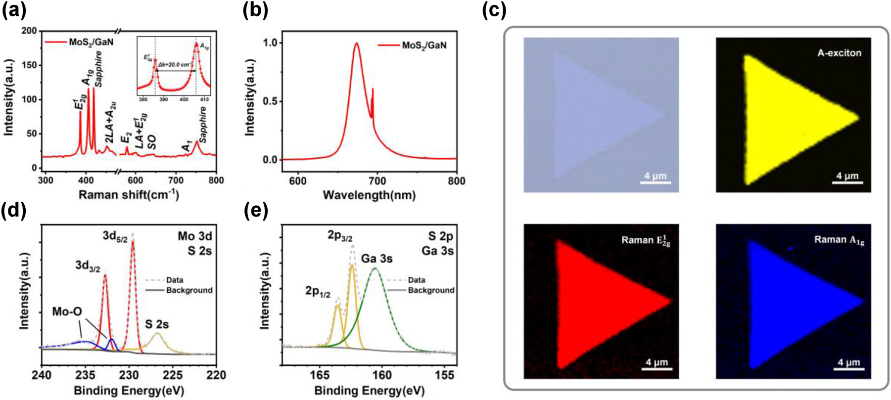
The composition and quality characterizations of the MoS2/GaN heterostructures. (a, b) Raman (a) and photoluminescence (b) spectra of monolayer MoS2 grown on GaN, respectively. The inset in (a) is a close-up view for the characteristic Raman modes of MoS2. (c) Optical microscopy image, PL intensity mapping for A-exciton, and Raman intensity mapping for
XPS spectra of the heterostructure are depicted in Figure 2(d), (e) and Figure S5. The Mo4+ 3d 5/2 and 3d 3/2 peaks are located at 229.5 eV and 232.7 eV, while the S2− 2p 3/2 and 2p 1/2 peaks are located at 162.3 eV and 163.5 eV, respectively, consistent with the corresponding binding energies reported in the literature for MoS2 single crystal [41]. Also, the stoichiometric ratio between S and Mo from the intensities of the respective XPS peaks could be calculated as S: Mo = 1.92: 1, further confirming the high quality of MoS2 nanosheets with few sulfur vacancies. In addition, the Ga 3s peak is observed at 160.5 eV (Figure 2(e)), together with Ga 2p 1/2 and Ga 2p 3/2 peaks at around 1145.4 and 1144.8 eV (Figure S5(a)), which are in line with the XPS spectra of GaN reported previously, further indicating the stability of GaN during the growth of MoS2 [42]. Moreover, there is no signature of any chemical state associated with Mo or S in the Ga 3d core level spectra (Figure S5(b)), suggesting atomically sharp heterointerface, which is clear evidence of a van der waals interaction between MoS2 and GaN.
3.2 Doping effect and exciton dynamics of monolayer MoS2 on differently doped GaN
According to previous reports, 2D layered MoS2 is sensitive to the surrounding environment, especially the substrates, that may dope the upper monolayer and thereby affect the exciton dynamics [43, 44]. To further reveal the doping effect and charge transfer properties of MoS2 in the heterostructures, monolayer MoS2 has been grown on differently doped GaN under the same condition and compared by Raman spectra. The optical resonance effects associated with the substrate’s geometrical features were largely ignored, since the structures were completely identical. Figure 3(a) depicts a comparison of the Raman spectra measured for monolayer MoS2 on differently doped GaN, in which the MoS2 on sapphire is also given as a reference. For the MoS2 on GaN, reduced frequency difference (Δk) between two Raman characteristic modes is observed, accompanied with blue-shift of the
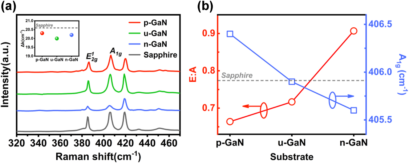
Effect of the differently doped GaN on the Raman modes of monolayer MoS2. (a) Raman spectra of monolayer MoS2 nanosheets on differently doped GaN and Sapphire. Inset is the frequency difference (Δk) between
To confirm the above findings, the PL spectra (excitation wavelength: 532 nm) of the monolayer MoS2 on all substrates were further analyzed by Lorentzian fitting of the experimental spectra in order to extract the individual excitonic transitions. Figure 4(a) shows three fitted exciton peaks of the monolayer MoS2 on different substrates, which are identified as neutral A and B excitons as well as negative trions (A−). The two neutral exciton emission peaks are ascribed to the splitting of valence-band maximum owing to the broken spatial-inversion symmetry in monolayer MoS2, whereas the trions (A−) are formed by the binding of a free electron to a neutral A exciton, represented as e + A → A− [48]. It is noteworthy that a larger PL intensity ratio of A exciton versus B exciton (A/B) can be observed in MoS2 on GaN, illustrating the excellent quality, as this ratio is considered an effective method to evaluate the crystal quality of MoS2 qualitatively [49]. Besides, the PL of monolayer MoS2 on p-GaN substrate is strongest among all the substrates we studied, around five times higher than that on sapphire substrate, while that on n-GaN substrate is the worst. These features indicate that the MoS2 systhesized on these substrates are differently n-doped, which will modulate the relative concentration of trions and neutral excitons [44]. Specifically, this relative concentration can be further analyzed by spectrum weight ratio I A−/I A, as displayed in Figure 4(b), where the I A and I A− are the integrated emission intensity of neutral excitons and trions, respectively [50, 51]. As it can be seen that, the I A−/I A ratios of MoS2 on p-GaN and u-GaN are much smaller than that on n-GaN, indicating the concentration of trions A-is lower in MoS2 on p-GaN and u-GaN. Therefore, it can be concluded that p-GaN can attract electrons from monolayer MoS2 and weaken its intrinsic n-doping while n-GaN provides electrons and enhance the n-doping level. Meanwhile, since trion emission has lower efficiency and broader spectrum compared to the exciton emission [44, 51], the normalized PL intensity of monolayer MoS2 decreases when the substrate changes from p-GaN, u-GaN to n-GaN.
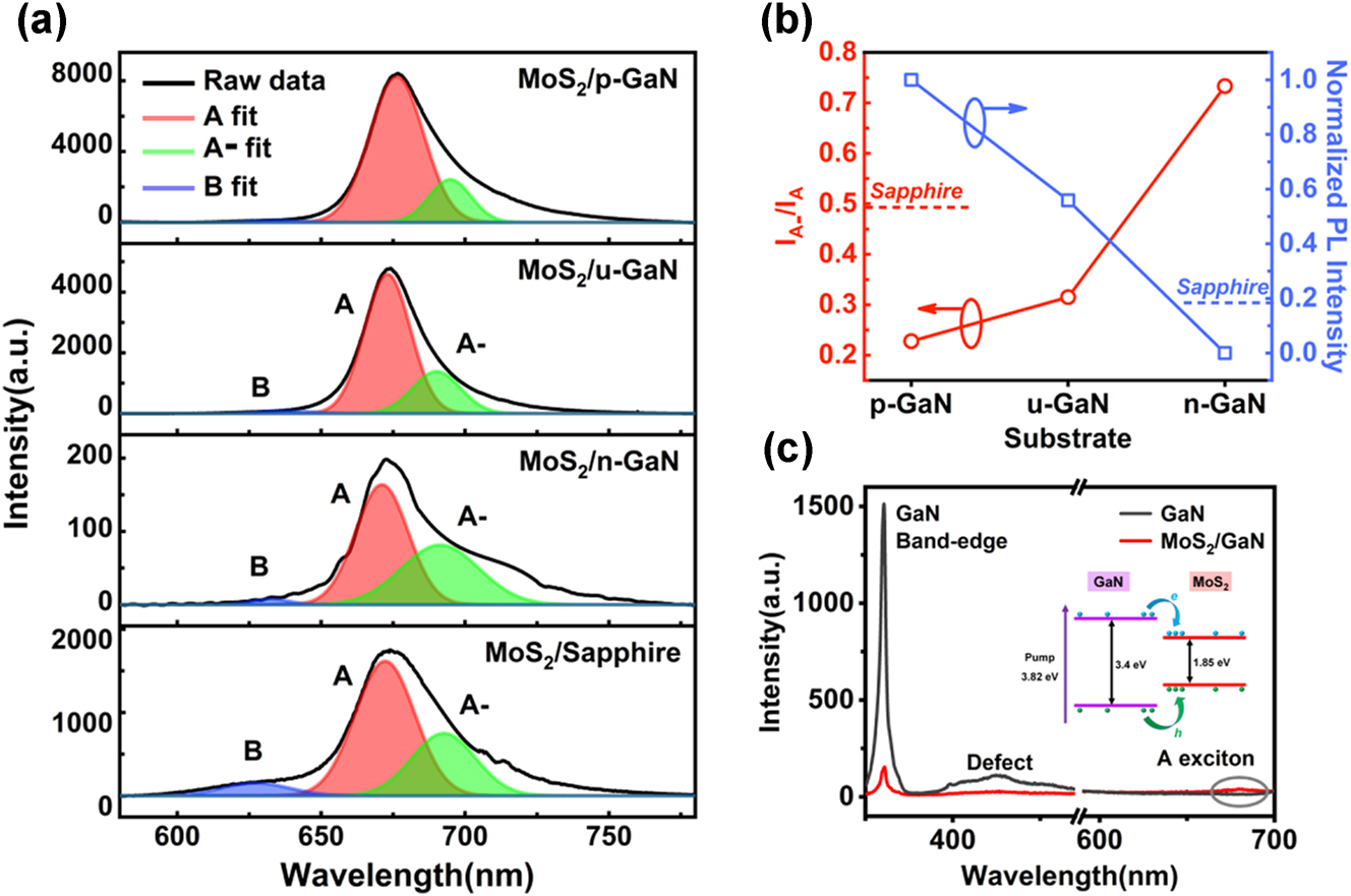
Effect of the differently doped GaN on the photoluminescence of monolayer MoS2. (a) PL spectra (excitation wavelength: 532 nm) and corresponding exciton peak fitting of monolayer MoS2 on p-GaN, u-GaN, n-GaN and sapphire. The neutral A exciton (red), B exciton (blue) and negative A-trion (green) fit are indicated together with the resulting cumulative spectrum (black). (b) The spectrum weight ratio I A−/I A and normalized PL intensity as a function of the doping type of GaN. (c) PL spectra (excitation wavelength: 325 nm) of MoS2/u-GaN heterostructure and bare u-GaN. Inset shows the schematic of the charge transfer at the MoS2/GaN heterointerface under such excitation.
To further elucidate the charge transfer process in MoS2/GaN heterostructures, different excitation sources were employed to excite GaN and MoS2/GaN heterostructures, respectively. Figure 4(c) displays the PL spectra of the MoS2/u-GaN heterostructures under the excitation of a 325 nm laser excitation. The PL spectrum of u-GaN consists of its band-edge emission centered at 360 nm as well as a weak defect emission centered around 450 nm. However, these two emissions are remarkably weakened in MoS2/u-GaN heterostructures, owing to the type I band alignment at the heterointerface, which facilitates the transfer of the photocarriers in GaN to monolayer MoS2 [16, 33]. More details about the band alignment of our samples are described in Supplementary Information (Note 1), based on the Kelvin probe force microscopy (KPFM) measurements (Figure S6), UPS spectra (Figure S7) and the established band diagram (Figure S8). Notably, the PL intensity of MoS2 is observed to be relatively weak, which can be attributed to the dominant non-radiative recombination of the hot carriers excited by such high photon energy [52]. In addition, the PL spectra of the heterostructures formed by MoS2 and other doped GaN is shown in Figure S9. Faint band-edge emission and defect emission of GaN in those heterostructures can also be observed, further verifying the efficient charge transfer process in MoS2/GaN heterostructures.
To understand the ultrafast exciton dynamics in the MoS2 on differently doped GaN, pump-probe TA measurements were performed (details are provided in the Experimental Section). The transient absorption spectra decay from different samples after photoexcitation of 400 nm with density of 100 μJ/cm2 are depicted in Figure 5(a–c). The spectra of monolayer MoS2 on differently doped GaN at different pump–probe delay times all feature the same three prominent negative peaks A, B and C, which are ascribed to the ground-state bleaching (GSB) due to Pauli blocking or state filling of the excitonic resonances. The lower energy peaks A at ∼ 670 nm and B at ∼ 615 nm correspond to excitonic transitions located at the K point. The higher energy peak C near 450 nm can be assigned to band nesting transition in different regions of the Brillouin zone, especially at the Γ point [53, 54]. The two positive peaks A* (685 nm) and B* (640 nm), at the right side of bleaching peaks A and B, respectively, can be attributed to the band gap renormalization and broadening photoinduced absorption [53]. It is also worth mentioning that both A and B excitonic bands of MoS2 on GaN show a red-shift compared to those on sapphire (Figure S10), which could be caused by the exciton–phonon coupling in the heterostructures [16].
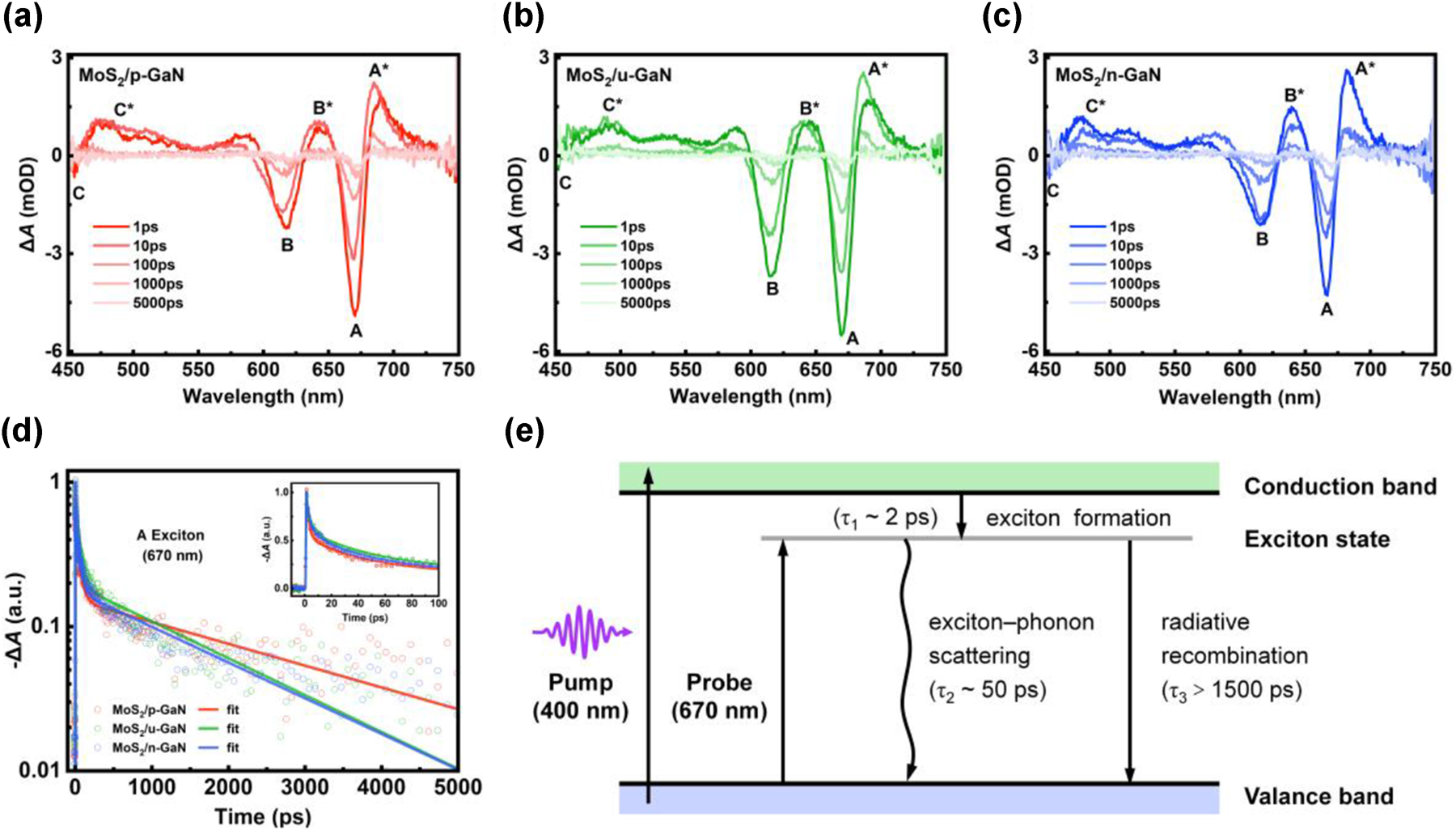
Effect of the differently doped GaN on the exciton dynamics of monolayer MoS2. (a–c) Transient absorption spectra of the monolayer MoS2 on p-GaN (a), u-GaN (b) and n-GaN (c) at different delay times, respectively, under excitations with fixed pump density of 100 μJ/cm2. (d) The kinetics traces of the A exciton state extracted from the TA results of samples with three doping types. The inset is a zoom-in view of the early 100 ps. The open circles are experimental data, the solid lines are the exponential fitting described in the main text, with consideration of the instrument response function (∼100 fs). (e) Schematic of the exciton dynamics in monolayer MoS2 on GaN.
In Figure 5(d), we summarize the normalized kinetics of A exciton of the three samples extracted from the TA spectra, so that we are able to quantitatively analyze the dynamics. All relaxation dynamics exhibit a multi-exponential decay trend, and can be fitted well by a tri-exponential function of [55, 56]:
where A 1, A 2 and A 3 represent the respective amplitude of lifetime τ 1, τ 2, and τ 3. The fitting parameters are tabulated in Table 1. The carrier relaxation processes for the A excitons are illustrated in Figure 5(e). The fast decay components (see the inset of Figure 5(e)) τ 1 of ∼2 ps are assigned to the formation process of exciton from free electron-hole pairs under nonresonant excitation [57, 58], with consistent proportion of the whole decay process in a range of 40–50 % for all three samples. The slow components τ 2 are in the same time scale of ∼50 ps for all samples with differently doped GaN substrates. The decay with τ 2 may be attributed to the exciton–phonon scattering process, since the excitons generated in MoS2 are strongly coupled to GaN phonons via the 2D material–substrate interaction, then lose their energy to the crystal lattice by emitting phonons in GaN [16, 59]. Remarkably, the long decay components τ 3 associated to the radiative recombination of excitons [56, 60], exist a strong correlation to the doping type of GaN. For the MoS2/p-GaN sample, the τ 3 process takes 2800 ps, apparently longer than those in samples of MoS2/u-GaN (1756 ps) and MoS2/n-GaN (1680 ps). The prolonged exciton lifetime during radiative recombination in MoS2/p-GaN can be attributed to the increased concentration of exciton with longer lifetime and reduced concentration of trion with shorter lifetime caused by substrate doping, which is consistent with the lowest spectrum weight ratio I A−/I A shown above [44].
Fitting parameters of the kinetic traces of A-exciton decay (extracted at 670 nm) in MoS2/p-GaN, MoS2/u-GaN and MoS2/n-GaN heterostructures, under excitation of 400 nm.
| Sample | A 1 | τ 1 (ps) | A 2 | τ 2 (ps) | A 3 | τ 3 (ps) |
|---|---|---|---|---|---|---|
| MoS2/p-GaN | 51.9 % | 1.932 | 34.3 % | 50.30 | 13.8 % | 2873 |
| MoS2/u-GaN | 40.7 % | 2.400 | 40.6 % | 53.40 | 18.7 % | 1730 |
| MoS2/n-GaN | 43.5 % | 2.800 | 40.0 % | 48.60 | 16.5 % | 1656 |
4 Conclusions
In summary, we have successfully demonstrated a simple and cost-efficient method for large-scale fabrication of MoS2/GaN heterostructures by pre-spinning a mixed solution of Na2MoO4 and NaOH on GaN substrates followed by CVD sulfurization. Large triangle-shaped monolayer MoS2 single-crystal nanosheets with side length more than 400 μm were achieved on differently doped GaN, covering almost 90 % of the surface. Moreover, it is found that the doping type of GaN can significantly modulate the n-doping level of MoS2 via the substrate doping effect. The PL intensity is enhanced and the exciton radiative recombination lifetime is prolonged in monolayer MoS2 on p-GaN due to the increased exciton concentration and reduced trion concentration. Our work hereby opens a pathway for large-scale fabrication of MoS2/GaN heterostructures, as well as an insight into their charge transfer properties and exciton dynamics, which should be beneficial to develop optoelectronic devices based on this heterostructure.
Supporting Information
Epitaxial structures of differently doped GaN; Schematic diagrams of MoS2 monolayer grown by our CVD method; additional results on XPS spectra of MoS2/GaN heterostructures; Optical microscopy images, KPFM measurements, UPS spectra, PL spectra and band diagrams of MoS2/p-GaN and MoS2/n-GaN heterostructures; Transient absorption spectra of the monolayer MoS2 on Sapphire.
Funding source: Fundamental Research Funds for the Central Universities
Award Identifier / Grant number: Grant No. 2020kfyXJJS124
Funding source: Key Laboratory of Infrared Imaging Materials and Detectors, the Shanghai Institute of Technical Physics, the Chinese Academy of Sciences
Award Identifier / Grant number: Grant No. IIMDKFJJ-21-07
Funding source: Natural Science Foundation of Hubei Province
Award Identifier / Grant number: Grant No.2022CFB011
Funding source: Key Research and Development Program of Hubei Province
Award Identifier / Grant number: Grant No. 2021BAA071
Funding source: National Natural Science Foundation of China
Award Identifier / Grant number: Grant No. 61974174
Award Identifier / Grant number: Grant No. 62174061
Award Identifier / Grant number: Grant No. 62174063
Funding source: National Key Research and Development Program of China
Award Identifier / Grant number: Grant No. 2022YFB3605104
Award Identifier / Grant number: Grant No. 2022YFB3604901
-
Research funding: This work was supported by the National Key Research and Development Program of China (Grant No. 2022YFB3604901), the National Natural Science Foundation of China (Grant No. 62174063, 62174061, 61974174), the National Key Research and Development Program of China (Grant No. 2022YFB3605104), the Key Research and Development Program of Hubei Province (Grant No. 2021BAA071), the Natural Science Foundation of Hubei Province (Grant No. 2022CFB011), the Key Laboratory of Infrared Imaging Materials and Detectors, the Shanghai Institute of Technical Physics, the Chinese Academy of Sciences (Grant No. IIMDKFJJ-21-07), and the Fundamental Research Funds for the Central Universities (Grant No. 2020kfyXJJS124).
-
Author contributions: All authors have accepted responsibility for the entire content of this manuscript and approved its submission.
-
Conflict of interest: Authors state no conflicts of interest.
-
Data availability: The datasets generated and/or analyzed during the current study are available from the corresponding author upon reasonable request.
References
[1] E. Singh, P. Singh, K. S. Kim, G. Y. Yeom, and H. S. Nalwa, “Flexible molybdenum disulfide (MoS2) atomic layers for wearable electronics and optoelectronics,” ACS Appl. Mater. Interfaces, vol. 11, pp. 11061–11105, 2019. https://doi.org/10.1021/acsami.8b19859.Search in Google Scholar PubMed
[2] A. Kuppadakkath, E. Najafidehaghani, Z. Gan, et al.., “Direct growth of monolayer MoS2 on nanostructured silicon waveguides,” Nanophotonics, vol. 11, pp. 4397–4408, 2022. https://doi.org/10.1515/nanoph-2022-0235.Search in Google Scholar
[3] R. Kumar, W. Zheng, X. Liu, J. Zhang, and M. Kumar, “MoS2‐Based nanomaterials for room‐temperature gas sensors,” Adv. Mater. Technol., vol. 5, p. 1901062, 2020. https://doi.org/10.1002/admt.201901062.Search in Google Scholar
[4] M. Liu, Y. Xu, Y. Hu, et al.., “Electrostatically charged MoS2/graphene oxide hybrid composites for excellent electrochemical energy storage devices,” ACS Appl. Mater. Interfaces, vol. 10, pp. 35571–35579, 2018. https://doi.org/10.1021/acsami.8b09085.Search in Google Scholar PubMed
[5] L. Ma, L. Yang, Y. Fang, et al.., “Observation of room-temperature out-of-plane switchable electric polarization in supported 3R-MoS2 monolayers,” SmartMat, vol. 4, p. e1161, 2023. https://doi.org/10.1002/smm2.1161.Search in Google Scholar
[6] C. Chang, W. Chen, Y. Chen, et al.., “Recent progress on two-dimensional materials,” Acta Phys.-Chim. Sin., vol. 37, p. 2108017, 2021. https://doi.org/10.3866/pku.whxb202108017.Search in Google Scholar
[7] H. W. Guo, Z. Hu, Z. B. Liu, and J. G. Tian, “Stacking of 2D materials,” Adv. Funct. Mater., vol. 31, p. 2007810, 2020. https://doi.org/10.1002/adfm.202007810.Search in Google Scholar
[8] Z. Chen, H. Liu, X. Chen, G. Chu, S. Chu, and H. Zhang, “Wafer-size and single-crystal MoSe2 atomically thin films grown on GaN substrate for light emission and harvesting,” ACS Appl. Mater. Interfaces, vol. 8, pp. 20267–20273, 2016. https://doi.org/10.1021/acsami.6b04768.Search in Google Scholar PubMed
[9] X. Zhang, J. Li, Z. Ma, J. Zhang, B. Leng, and B. Liu, “Design and integration of a layered MoS2/GaN van der Waals heterostructure for wide spectral detection and enhanced photoresponse,” ACS Appl. Mater. Interfaces, vol. 12, pp. 47721–47728, 2020. https://doi.org/10.1021/acsami.0c11021.Search in Google Scholar PubMed
[10] S. Lin, Y. Lu, J. Xu, S. Feng, and J. Li, “High performance graphene/semiconductor van der Waals heterostructure optoelectronic devices,” Nano Energy, vol. 40, pp. 122–148, 2017. https://doi.org/10.1016/j.nanoen.2017.07.036.Search in Google Scholar
[11] J. Y. Yang, M. Park, M. J. Yeom, et al.., “Reconfigurable physical reservoir in GaN/α-In2Se3 HEMTs enabled by out-of-plane local polarization of ferroelectric 2D layer,” ACS Nano, vol. 17, pp. 7695–7704, 2023. https://doi.org/10.1021/acsnano.3c00187.Search in Google Scholar PubMed
[12] A. Khan, K. Balakrishnan, and T. Katona, “Ultraviolet light-emitting diodes based on group three nitrides,” Nat. Photonics, vol. 2, pp. 77–84, 2008. https://doi.org/10.1038/nphoton.2007.293.Search in Google Scholar
[13] H. Wang, H. You, Y. Xu, et al.., “High-responsivity and fast-response ultraviolet phototransistors based on enhanced p-GaN/AlGaN/GaN HEMTs,” ACS Photonics, vol. 9, pp. 2040–2045, 2022. https://doi.org/10.1021/acsphotonics.2c00177.Search in Google Scholar
[14] Y. Wu, Z. W. Li, K. W. Ang, et al.., “Monolithic integration of MoS2-based visible detectors and GaN-based UV detectors,” Photonics Res., vol. 7, pp. 1127–1133, 2019. https://doi.org/10.1364/prj.7.001127.Search in Google Scholar
[15] Y. Wan, J. Xiao, J. Li, et al.., “Epitaxial single‐layer MoS2 on GaN with enhanced valley helicity,” Adv. Mater., vol. 30, p. 1703888, 2018. https://doi.org/10.1002/adma.201703888.Search in Google Scholar PubMed
[16] Y. Poudel, J. Sławińska, P. Gopal, et al.., “Absorption and emission modulation in a MoS2–GaN (0001) heterostructure by interface phonon–exciton coupling,” Photonics Res., vol. 7, p. 1511, 2019. https://doi.org/10.1364/prj.7.001511.Search in Google Scholar
[17] P. Wang, C. Chang, S. Lin, J. Sheu, and C. Sun, “Temporally probing the thermal phonon and charge transfer induced out-of-plane acoustical displacement of monolayer and bi-layer MoS2/GaN heterojunction,” Photoacoustics, vol. 30, p. 100477, 2023. https://doi.org/10.1016/j.pacs.2023.100477.Search in Google Scholar PubMed PubMed Central
[18] B. Cao, S. Ma, W. Wang, et al.., “Charge redistribution in Mg-doped p-type MoS2/GaN photodetectors,” J. Phys. Chem. C, vol. 126, pp. 18893–18899, 2022. https://doi.org/10.1021/acs.jpcc.2c05895.Search in Google Scholar
[19] S. Xing, G. Zhao, B. Mao, et al.., “The same band alignment of two hybrid 2D/3D vertical heterojunctions formed by combining monolayer MoS2 with semi-polar (11–22) GaN and c-plane (0001) GaN,” Appl. Surf. Sci., vol. 599, p. 153965, 2022. https://doi.org/10.1016/j.apsusc.2022.153965.Search in Google Scholar
[20] S. K. Jain, M. X. Low, P. D. Taylor, et al.., “2D/3D hybrid of MoS2/GaN for a high-performance broadband photodetector,” ACS Appl. Electron. Mater., vol. 3, pp. 2407–2414, 2021. https://doi.org/10.1021/acsaelm.1c00299.Search in Google Scholar
[21] C. Liu, Y. Lu, X. Yu, et al.., “Hot carriers assisted mixed-dimensional graphene/MoS2/p-GaN light emitting diode,” Carbon, vol. 197, pp. 192–199, 2022. https://doi.org/10.1016/j.carbon.2022.06.025.Search in Google Scholar
[22] F. Wang, D. Chang, Z. Wang, and H. Cui, “Dual-wavelength photodetector based on monolayer MoS2/GaN heterostructure,” Appl. Phys. A, vol. 128, p. 418, 2022. https://doi.org/10.1007/s00339-022-05555-4.Search in Google Scholar
[23] P. Yang, H. Yang, Z. Wu, et al.., “Large-area monolayer MoS2 nanosheets on GaN substrates for light-emitting diodes and valley-spin electronic devices,” ACS Appl. Nano Mater., vol. 4, pp. 12127–12136, 2021. https://doi.org/10.1021/acsanm.1c02662.Search in Google Scholar
[24] H. Liu, G. Qi, C. Tang, et al.., “Growth of large-area homogeneous monolayer transition-metal disulfides via a molten liquid intermediate process,” ACS Appl. Mater. Interfaces, vol. 12, pp. 13174–13181, 2020. https://doi.org/10.1021/acsami.9b22397.Search in Google Scholar PubMed
[25] S. Li, Y. Lin, W. Zhao, et al.., “Vapour–liquid–solid growth of monolayer MoS2 nanoribbons,” Nat. Mater., vol. 17, pp. 535–542, 2018. https://doi.org/10.1038/s41563-018-0055-z.Search in Google Scholar PubMed
[26] Z. Gan, E. Najafidehaghani, S. H. Han, et al.., “Patterned growth of transition metal dichalcogenide monolayers and multilayers for electronic and optoelectronic device applications,” Small Methods, vol. 6, p. 2200300, 2022. https://doi.org/10.1002/smtd.202200300.Search in Google Scholar PubMed
[27] S. Li, Y. Lin, X. Liu, et al.., “Wafer-scale and deterministic patterned growth of monolayer MoS2 via vapor–liquid–solid method,” Nanoscale, vol. 11, pp. 16122–16129, 2019. https://doi.org/10.1039/c9nr04612g.Search in Google Scholar PubMed
[28] P. Jian, S. Tan, Z. Zheng, et al.., “Controllable synthesis of high-aspect-ratio monolayer MoS2 nano-microribbons for high-performance phototransistors,” Sci. China Mater., vol. 66, pp. 3941–3948, 2023. https://doi.org/10.1007/s40843-023-2569-8.Search in Google Scholar
[29] S. Wang, Y. Zhang, D. Zhao, et al.., “Fast and controllable synthesis of AB-stacked bilayer MoS2 for photoelectric detection,” 2d materials, vol. 9, p. 15016, 2021. https://doi.org/10.1088/2053-1583/ac395f.Search in Google Scholar
[30] S. Hu, J. Li, X. Zhan, et al.., “Aligned monolayer MoS2 ribbons growth on sapphire substrate via NaOH-assisted chemical vapor deposition,” Sci. China Mater., vol. 63, pp. 1065–1075, 2020. https://doi.org/10.1007/s40843-019-1265-9.Search in Google Scholar
[31] P. Desai, B. Todankar, A. K. Ranade, et al.., “Synthesis of MoS2 layers on GaN using ammonium tetrathiomolybdate for heterojunction device applications,” Cryst. Res. Technol., vol. 56, p. 2000198, 2021. https://doi.org/10.1002/crat.202000198.Search in Google Scholar
[32] G. Yang, Y. Ding, N. Lu, et al.., “Insights into the two-dimensional MoS2 grown on AlGaN(GaN) substrates by CVD method,” IEEE Photonics J., vol. 13, pp. 1–5, 2021. https://doi.org/10.1109/jphot.2021.3120797.Search in Google Scholar
[33] J. Lee, H. Jang, T. Kwak, U. Choi, B. So, and O. Nam, “Growth and characterization of MoS2/n-GaN and MoS2/p-GaN vertical heterostructure with wafer scale homogeneity,” Solid-State Electron., vol. 165, p. 107751, 2020. https://doi.org/10.1016/j.sse.2019.107751.Search in Google Scholar
[34] P. Yan, Q. Tian, G. Yang, et al.., “Epitaxial growth and interfacial property of monolayer MoS2 on gallium nitride,” RSC Adv., vol. 8, pp. 33193–33197, 2018. https://doi.org/10.1039/c8ra04821e.Search in Google Scholar PubMed PubMed Central
[35] P. Yan, J. Wang, G. Yang, et al.., “Chemical vapor deposition of monolayer MoS2 on sapphire, Si and GaN substrates,” Superlattices Microstruct., vol. 120, pp. 235–240, 2018. https://doi.org/10.1016/j.spmi.2018.05.049.Search in Google Scholar
[36] T. P. O’Regan, D. Ruzmetov, M. R. Neupane, et al.., “Structural and electrical analysis of epitaxial 2D/3D vertical heterojunctions of monolayer MoS2 on GaN,” Appl. Phys. Lett., vol. 111, p. 051602, 2017. https://doi.org/10.1063/1.4997188.Search in Google Scholar
[37] D. Ruzmetov, K. Zhang, G. Stan, et al.., “Vertical 2D/3D semiconductor heterostructures based on epitaxial molybdenum disulfide and gallium nitride,” ACS Nano, vol. 10, pp. 3580–3588, 2016. https://doi.org/10.1021/acsnano.5b08008.Search in Google Scholar PubMed
[38] X. Zhang, X. Qiao, W. Shi, J. Wu, D. Jiang, and P. Tan, “Phonon and Raman scattering of two-dimensional transition metal dichalcogenides from monolayer, multilayer to bulk material,” Chem. Soc. Rev., vol. 44, pp. 2757–2785, 2015. https://doi.org/10.1039/c4cs00282b.Search in Google Scholar PubMed
[39] Y. Yu, C. Li, Y. Liu, L. Su, Y. Zhang, and L. Cao, “Controlled scalable synthesis of uniform, high-quality monolayer and few-layer MoS2 films,” Sci. Rep., vol. 3, p. 1866, 2013. https://doi.org/10.1038/srep01866.Search in Google Scholar PubMed PubMed Central
[40] S. Parida, A. Patsha, S. Bera, and S. Dhara, “Spectroscopic investigation of native defect induced electron-phonon coupling in GaN nanowires,” J. Phys. D: Appl. Phys., vol. 50, p. 7, 2017. https://doi.org/10.1088/1361-6463/aa7402.Search in Google Scholar
[41] K. Liu, W. Zhang, Y. Lee, et al.., “Growth of large-area and highly crystalline MoS2 thin layers on insulating substrates,” Nano Lett., vol. 12, pp. 1538–1544, 2012. https://doi.org/10.1021/nl2043612.Search in Google Scholar PubMed
[42] R. Carin, J. P. Deville, and J. Werckmann, “An XPS study of GaN thin films on GaAs,” Surf. Interface Anal., vol. 16, pp. 65–69, 1990. https://doi.org/10.1002/sia.740160116.Search in Google Scholar
[43] C. Lattyak, M. Vehse, M. A. Gonzalez, et al.., “Optoelectronic properties of MoS2 in proximity to carrier selective metal oxides,” Adv. Opt. Mater., vol. 10, p. 2102226, 2022. https://doi.org/10.1002/adom.202102226.Search in Google Scholar
[44] Y. Yu, Y. Yu, C. Xu, et al.., “Engineering substrate interactions for high luminescence efficiency of transition-metal dichalcogenide monolayers,” Adv. Funct. Mater., vol. 26, pp. 4733–4739, 2016. https://doi.org/10.1002/adfm.201600418.Search in Google Scholar
[45] A. Castellanos-Gomez, R. Roldan, E. Cappelluti, et al.., “Local strain engineering in atomically thin MoS2,” Nano Lett., vol. 13, pp. 5361–5366, 2013. https://doi.org/10.1021/nl402875m.Search in Google Scholar PubMed
[46] A. Bera, D. V. S. Muthu, S. Bhowmick, U. V. Waghmare, A. K. Sood, and B. Chakraborty, “Symmetry-dependent phonon renormalization in monolayer MoS2 transistor,” Phys. Rev. B, vol. 85, p. 161403, 2012. https://doi.org/10.1103/physrevb.85.161403.Search in Google Scholar
[47] W. H. Chae, J. D. Cain, E. D. Hanson, A. A. Murthy, and V. P. Dravid, “Substrate-induced strain and charge doping in CVD-grown monolayer MoS2,” Appl. Phys. Lett., vol. 111, p. 143106, 2017. https://doi.org/10.1063/1.4998284.Search in Google Scholar
[48] M. Tebyetekerwa, J. Zhang, Z. Xu, et al.., “Mechanisms and applications of steady-state photoluminescence spectroscopy in two-dimensional transition-metal dichalcogenides,” ACS Nano, vol. 14, pp. 14579–14604, 2020. https://doi.org/10.1021/acsnano.0c08668.Search in Google Scholar PubMed
[49] K. M. McCreary, A. T. Hanbicki, S. V. Sivaram, and B. T. Jonker, “A- and B-exciton photoluminescence intensity ratio as a measure of sample quality for transition metal dichalcogenide monolayers,” APL Mater., vol. 6, pp. 111106–111106-9, 2018. https://doi.org/10.1063/1.5053699.Search in Google Scholar
[50] Y. Li, Z. Qi, M. Liu, et al.., “Photoluminescence of monolayer MoS2 on LaAlO3 and SrTiO3 substrates,” Nanoscale, vol. 6, pp. 15248–15254, 2014. https://doi.org/10.1039/c4nr04602a.Search in Google Scholar PubMed
[51] K. F. Mak, K. He, C. Lee, et al.., “Tightly bound trions in monolayer MoS2,” Nat. Mater., vol. 12, pp. 207–211, 2013. https://doi.org/10.1038/nmat3505.Search in Google Scholar PubMed
[52] A. Steinhoff, J. H. Kim, F. Jahnke, et al.., “Efficient excitonic photoluminescence in direct and indirect band gap monolayer MoS2,” Nano Lett., vol. 15, pp. 6841–6847, 2015. https://doi.org/10.1021/acs.nanolett.5b02719.Search in Google Scholar PubMed
[53] H. Liu, P. Tan, Y. Liu, et al.., “Ultrafast interfacial charge evolution of the Type-II cadmium Sulfide/Molybdenum disulfide heterostructure for photocatalytic hydrogen production,” J. Colloid Interface Sci., vol. 619, pp. 246–256, 2022. https://doi.org/10.1016/j.jcis.2022.03.080.Search in Google Scholar PubMed
[54] T. Voelzer, F. Fennel, T. Korn, and S. Lochbrunner, “Fluence-dependent dynamics of localized excited species in monolayer versus bulk MoS2,” Phys. Rev. B, vol. 103, p. 045423, 2021. https://doi.org/10.1103/physrevb.103.045423.Search in Google Scholar
[55] D. X. Lu, Q. Zhou, F. F. Li, X. W. Li, and G. Y. Lu, “Influence of interlayer interactions on the relaxation dynamics of excitons in ultrathin MoS2,” Nanoscale Adv., vol. 1, pp. 1186–1192, 2019. https://doi.org/10.1039/c8na00086g.Search in Google Scholar PubMed PubMed Central
[56] H. Shi, R. Yan, S. Bertolazzi, et al.., “Exciton dynamics in suspended monolayer and few-layer MoS2 2D crystals,” ACS Nano, vol. 7, pp. 1072–1080, 2013. https://doi.org/10.1021/nn303973r.Search in Google Scholar PubMed
[57] Z. Nie, Y. Shi, S. Qin, et al.., “Tailoring exciton dynamics of monolayer transition metal dichalcogenides by interfacial electron-phonon coupling,” Commun. Phys., vol. 2, p. 103, 2019. https://doi.org/10.1038/s42005-019-0202-0.Search in Google Scholar
[58] F. Ceballos, Q. Cui, M. Z. Bellus, and H. Zhao, “Exciton formation in monolayer transition metal dichalcogenides,” Nanoscale, vol. 8, pp. 11681–11688, 2016. https://doi.org/10.1039/c6nr02516a.Search in Google Scholar PubMed
[59] T. Korn, S. Heydrich, M. Hirmer, J. Schmutzler, and C. Schüller, “Low-temperature photocarrier dynamics in monolayer MoS2,” Appl. Phys. Lett., vol. 99, p. 102109, 2011. https://doi.org/10.1063/1.3636402.Search in Google Scholar
[60] S. Bettis Homan, V. K. Sangwan, I. Balla, H. Bergeron, E. A. Weiss, and M. C. Hersam, “Ultrafast exciton dissociation and long-lived charge separation in a photovoltaic pentacene–MoS2 van der Waals heterojunction,” Nano Lett., vol. 17, pp. 164–169, 2017. https://doi.org/10.1021/acs.nanolett.6b03704.Search in Google Scholar PubMed
Supplementary Material
This article contains supplementary material (https://doi.org/10.1515/nanoph-2023-0503).
© 2023 the author(s), published by De Gruyter, Berlin/Boston
This work is licensed under the Creative Commons Attribution 4.0 International License.
Articles in the same Issue
- Frontmatter
- Reviews
- A newcomer’s guide to deep learning for inverse design in nano-photonics
- Information multiplexing from optical holography to multi-channel metaholography
- Research Articles
- Optical tuning of the terahertz response of black phosphorus quantum dots: effects of weak carrier confinement
- Tunable bound states in the continuum in active metasurfaces of graphene disk dimers
- Ultrafast dynamics and ablation mechanism in femtosecond laser irradiated Au/Ti bilayer systems
- Large-scale synthesis and exciton dynamics of monolayer MoS2 on differently doped GaN substrates
- Revealing defect-bound excitons in WS2 monolayer at room temperature by exploiting the transverse electric polarized wave supported by a Si3N4/Ag heterostructure
- Carrier transfer in quasi-2D perovskite/MoS2 monolayer heterostructure
- Concentric ring optical traps for orbital rotation of particles
- A compact weak measurement to observe the spin Hall effect of light