
Visible-mid infrared ultra-broadband and wide-angle metamaterial perfect absorber based on cermet films with nano-cone structure
-
Fan Yang

 and
Shao-Ji Jiang
and
Shao-Ji Jiang

Abstract
Metamaterial absorbers over a broadband spectrum with high absorption, good angular tolerance, and easy configurations have essential importance for optical and optoelectronic devices. In this study, a hybrid metamaterial absorber comprising multilayered cermet thin films (multi-cermet) with tapered structure is designed and experimentally demonstrated. Combining optical interference of multi-cermet films and optical field localization of nano-cone structures, the average absorbance of both simulation and measurement are more than 98% in an ultrabroad bandwidth (300–3000 nm), and the proposed absorber shows a good angular tolerance as well. The composite process of two easy-operated and efficient methods, colloidal lithography, and magnetron sputtering, is employed for large-area fabrication. In addition, owing to flexible polyimide substrate, the proposed absorber also shows good bending and heating resistance, which reflects its potential in engineering application.
1 Introduction
Metamaterial absorbers (MAs) with efficient absorbing properties at the visible and infrared wavelengths are attracting increasing interest, due to their potential optical applications including solar collection systems [1–5], thermal emitters [6–9], infrared imaging [10, 11], sensors [12–15] and photodetectors [16–18]. In order to meet the increasing demand of modern devices, it is necessary to achieve perfect absorption in a wide spectral band and maintain high absorbance under arbitrary incident angles. Thus, how to design and fabricate a perfect broadband absorber in the desired band should be of great concern.
Conventional perfect absorbers composed of metal–dielectric–metal (MDM) multilayer structures in the vertical direction are commonplace. In general, the response of this type of cavity is always angle-dependent and narrowband [19–24]. By employing a high-loss metal material and adding an impedance-matching layer atop, the absorption bandwidth can be broadened to a certain extent [25–27]. What’s more, numerous nanostructures have been brought up to broaden the bandwidth further and reduce the sensitivity to incident angle, such as pyramids, nanopillar, and nanoholes [19, 28], [29], [30]. However, most of these designs can only cover a part of the visible or near infrared (NIR) spectrum and their absorption bandwidth is inherently restricted. In addition, the existing manufacturing methods to realize these designs, have difficulty in achieving a good balance between high precision, time-consuming and cost [31, 32]. Thus, designing wide-angle and ultrabroadband perfect absorbers compatible with the currently used cost-effective industrial production technology remains a major challenge.
Here, as an initial step, we propose a planar multilayer cermet thin film (multi-cermet) absorber which is made of Cu/Zr–ZrO2 (HMVF, high metal volume fraction)/Zr–ZrO2 (MMVF, middle metal volume fraction)/Zr–ZrO2 (LMVF, low metal volume fraction)/Al2O3. Based on the optical interference of multi-cermet films, the designed multi-cermet absorber demonstrates well-matched impedance from 350 to 2670 nm, which leads to a good absorption (
2 Design and calculation
2.1 Design of planar multi-cermet absorber
To begin with, according to the law of energy conversation, the absorbance (A) can be calculated by the formula A = 1 − R − T, where R and T represent the reflectance and transmittance, respectively [33]. By designing a thick metal (Cu) as the bottom layer, the transmittance can be almost reduced to zero. Then, absorption can be maximized with the minimized reflection at the interface with air.
To reduce interface reflection, three-layered cermet and a dielectric coating (Al2O3) stacked in the vertical direction are designed. The order of cermet layers from bottom to top is HMVF, MMVF, and LMVF. Here, lower metal volume fraction leads to lower effective permittivity (ɛ eff) value of the cermet. Consequently, the proposed multi-cermet absorber has a gradually increasing ɛ eff from the upper air–structure interface to the lower structure–substrate interface which contributes to the impedance matching. The metal filling factor f is, respectively, set as f = 0.55 (HMVF), f = 0.25 (MMVF) and f = 0.15 (LMVF), considering the fabrication parameter. In addition, the test results of these metal filling factors were measured by energy dispersive spectroscopy (EDS) as shown in Table 1. Therefore, the planar multi-cermet absorber made of Cu/Zr–ZrO2 (HMVF, f = 0.55)/Zr–ZrO2 (MMVF, f = 0.25)/Zr–ZrO2 (LMVF, f = 0.15)/Al2O3 is designed as shown in Figure 1(a).
The results of EDS for cermet coatings.
| Materials | Atomic (%) | Metal filling factor f | |
|---|---|---|---|
| Zr | O | ||
| Zr–ZrO2 (HMVF) | 52.81 | 47.19 | 0.55 |
| Zr–ZrO2 (MMVF) | 40.15 | 59.85 | 0.25 |
| Zr–ZrO2 (LMVF) | 37.08 | 62.92 | 0.15 |
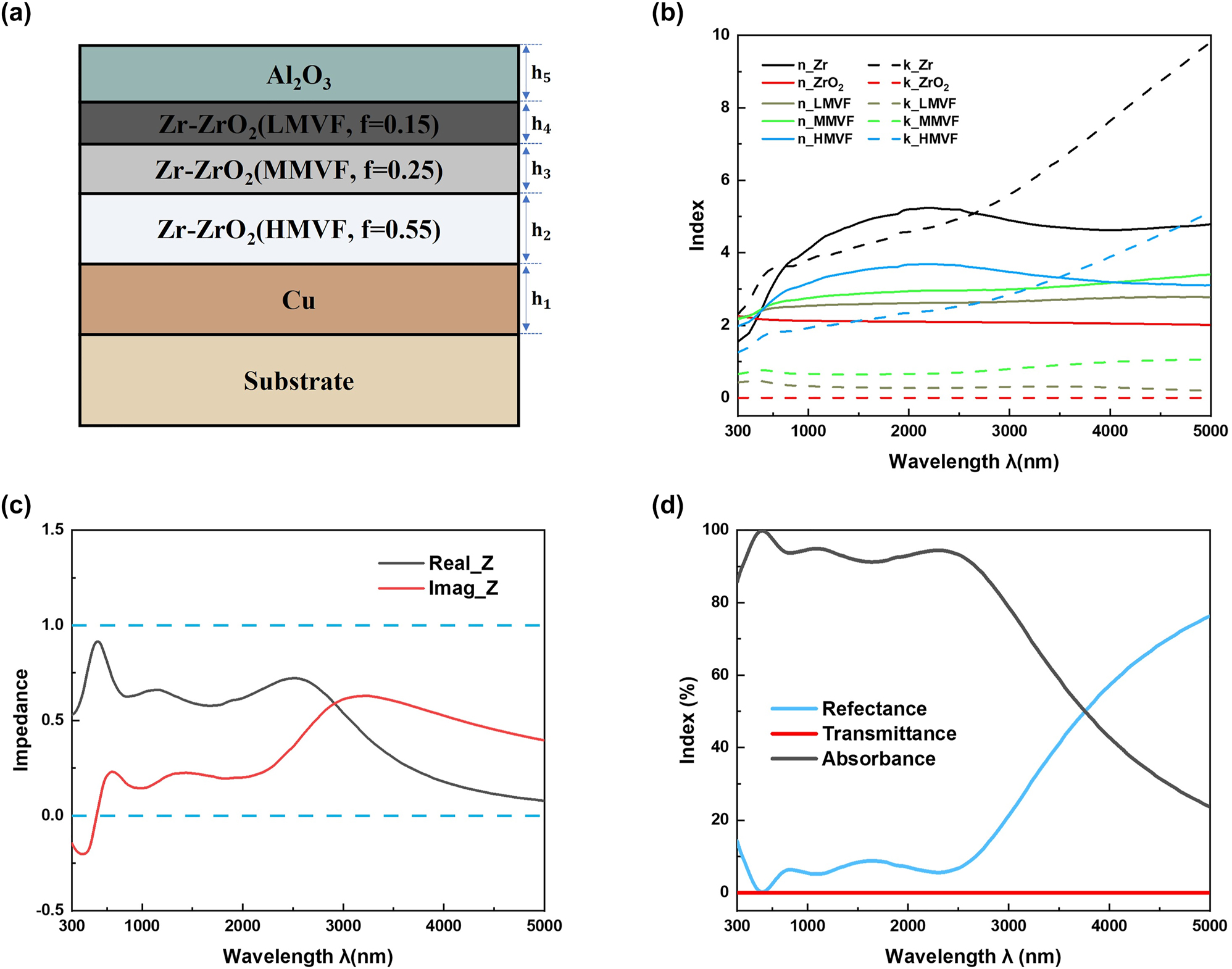
The simulation parameters and results of planar multi-cermet absorber. (a) The 2D schematic diagram of the planar multi-cermet absorber with structural parameters as h1 = 100 nm, h2 = 100 nm, h3 = 55 nm, h4 = 40 nm, h5 = 70 nm. (b) Refractive index n and extinction coefficient k of Zr–ZrO2 with different metal filling factor f. (c) Real (black line) and imaginary (red line) parts of the calculated impedance of the sample (the blue dotted lines represent the impedance of 0 and 1). (d) Simulated reflectance, transmittance, and the corresponding calculated absorbance of the proposed absorber at normal incidence.
To guide the design of multilayer-cermet film system, the equivalent optical parameters of cermet can be calculated quantitatively by effective-medium-theory (EMT) method. The EMT method is based on a model proposed by Ping Sheng (SH) which has been widely used for the dielectric function of a composite [34, 35]. In the SH theory, a probabilistic growth model for grains in a composite film has been introduced. The film is modeled as a mixture of two types of coated oblate spheroidal units, dielectric-coated metal spheroids described as type-a units and metal-coated dielectric spheroids described as type-b units [36]. For the simple case of spherical grains, the relative probability of the occurrence for type-a units J a at any metal volume fraction is given by [34, 36]
For type-b units, J b = 1 − J a . In the simple case of spherical grains, the average dielectric function of a composite in Sheng’s approximation, ɛ SH is given by [35]
where
Here, the ɛ a and ɛ b are the dielectric functions of type-a units and type-b units, respectively. The filling factor f a represents the volume fraction occupied by the type-a units. And the complex refractive index n + ik, is derived from the complex dielectric function ɛ = ɛ′ + iɛ″ using the relationship n + ik = ɛ 1/2. By using EMT, the refractive index n and extinction coefficient k of cermet could be calculated. Figure 1(b) presents the n and k of Zr–ZrO2 cermet with different metal filling factor. In the calculation, the optical constants of Zr are obtained from Ref. [37], the optical constants of ZrO2 are obtained from Ref. [38].
To reveal the absorption mechanism, we calculated the optical impedance Z of the multi-cermet absorber. In impedance theory, reflectance of absorber can be calculated by the formula,
2.2 Design of nano-cone metamaterial absorber
The planar multi-cermet absorber has already shown a good absorbability at a broadband region. However, it is sensitive to the incident angle and the absorption performance is limited. To tackle these drawbacks, we designed a nano-cone metamaterial absorber based on the planar one.
The proposed metamaterial absorbers were composed of multi-cermet films with nano-cone structure as shown in Figure 2(a) and (b) presents the cross-sectional view. The period (P), height (h0), and bottom diameters (L) of the cone are set as 1000 nm, 1000 nm, and 800 nm, respectively, and the thickness of the five-layered thin film from bottom to top (h1, h2, h3, h4, h5) is set as 100 nm, 100 nm, 55 nm, 40 nm, and 70 nm, respectively.
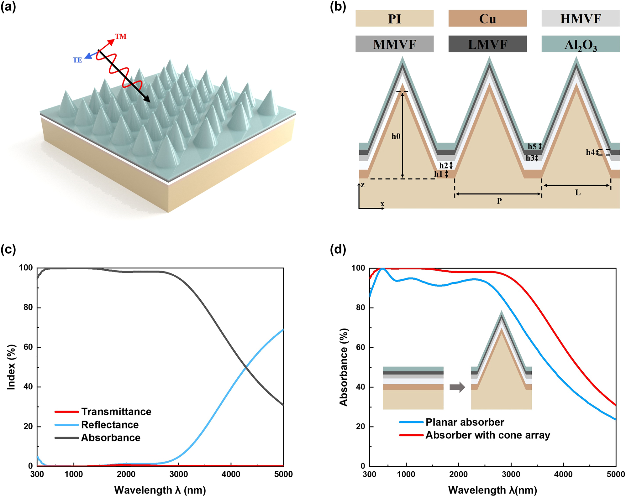
The simulation parameters and results of the designed nano-cone metamaterial absorber. (a) The 3D schematic diagram of the proposed nano-cone metamaterial absorber. (b) The cross-section configuration and structural parameters of the structure. (c) Simulated reflectance, transmittance, and the corresponding calculated absorbance of the proposed absorber at normal incidence. (d) Comparison of the calculated absorbance of the proposed nano-cone metamaterial absorber and the planar one.
The proposed absorber shown in Figure 2(a) and (b) is set up and systematically calculated by FDTD Solutions from LUMERICAL. The optical constant of Cu comes from Lorentz–Drude model with an experimental table data [40], the refractive index of Al2O3 is obtained from Ref. [41], the permittivity of PI is obtained from Refs. [42, 43] and the optical constant of Zr–ZrO2(f = 0.15, 0.25, 0.55) are obtained from the computed result as Figure 1(b) shows. Figure 2(c) depicts the simulated reflectance, transmittance, and the calculated absorbance of the proposed absorber when TM-polarized light is normally incident. The simulated transmittance is close to zero since the bottom Cu layer is much thicker than the penetration depth. Because of the additional light trapping structures, the proposed nano-cone metamaterial absorber presents better absorption performance than the planar one as shown in Figure 2(d). More specifically, it exhibits a high absorbance, greater than 95% in the range of 300–3000 nm, and the average absorbance is 98.7% in such a wide region.
Furthermore, the absorbance of different polarization states is calculated at normal incidence as shown in Figure 3(a). There is almost no difference between them due to the rotational symmetry of the designed structure. This result verifies the polarization-independence of the proposed absorber. The absorption spectrum is calculated for unpolarized light
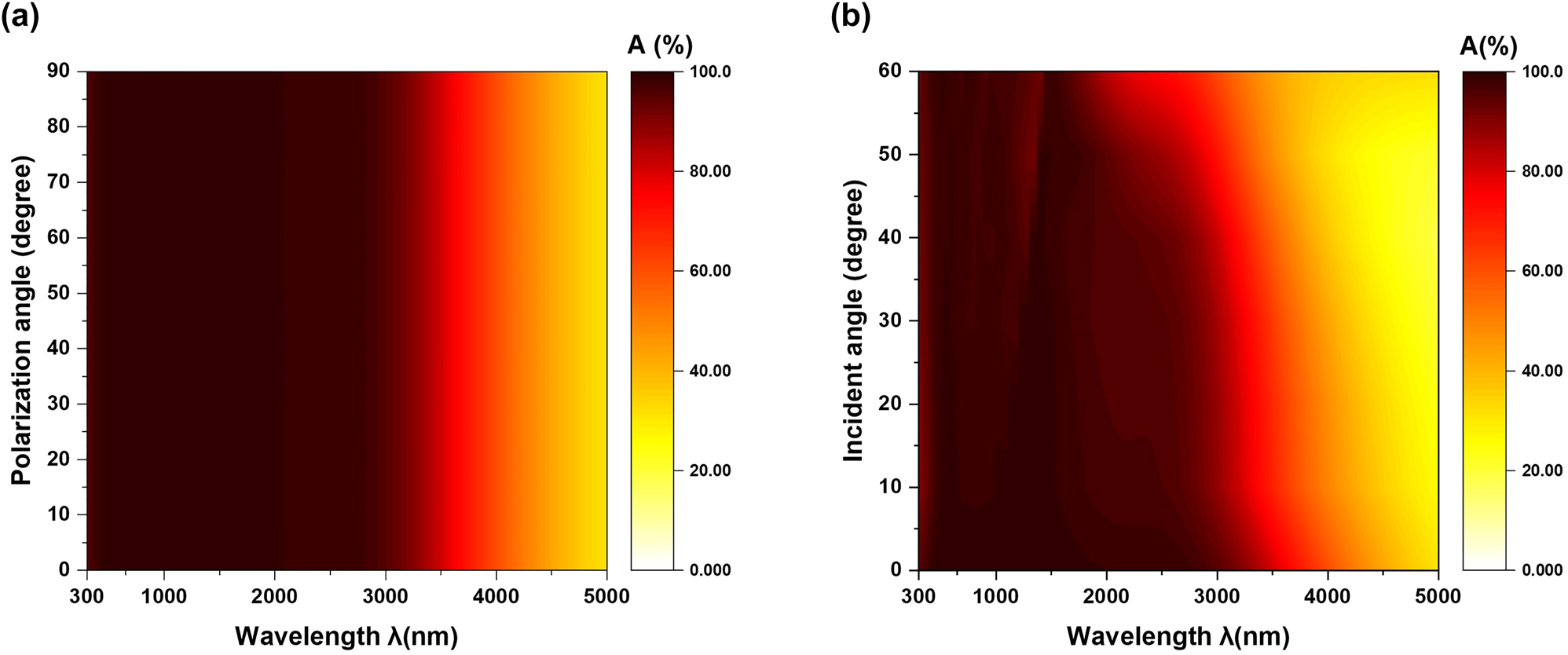
The simulated absorbance for different polarization angles and incident angles. (a) Calculated absorbance for different polarization angles from 0° to 90° at normal incidence. (b) Simulated absorption spectrum at different incident angles varying from 0° to 60° in 10° steps for unpolarized light.
We then simulated the electric field, magnetic field and heat power density distributions in our absorber at the specific incident wavelengths of 500 nm, 1500 nm, and 2500 nm, to further illustrate the underlying mechanism of the nano-cone light trapping structure as shown in Figure 4. The heat power density, Q is expressed as
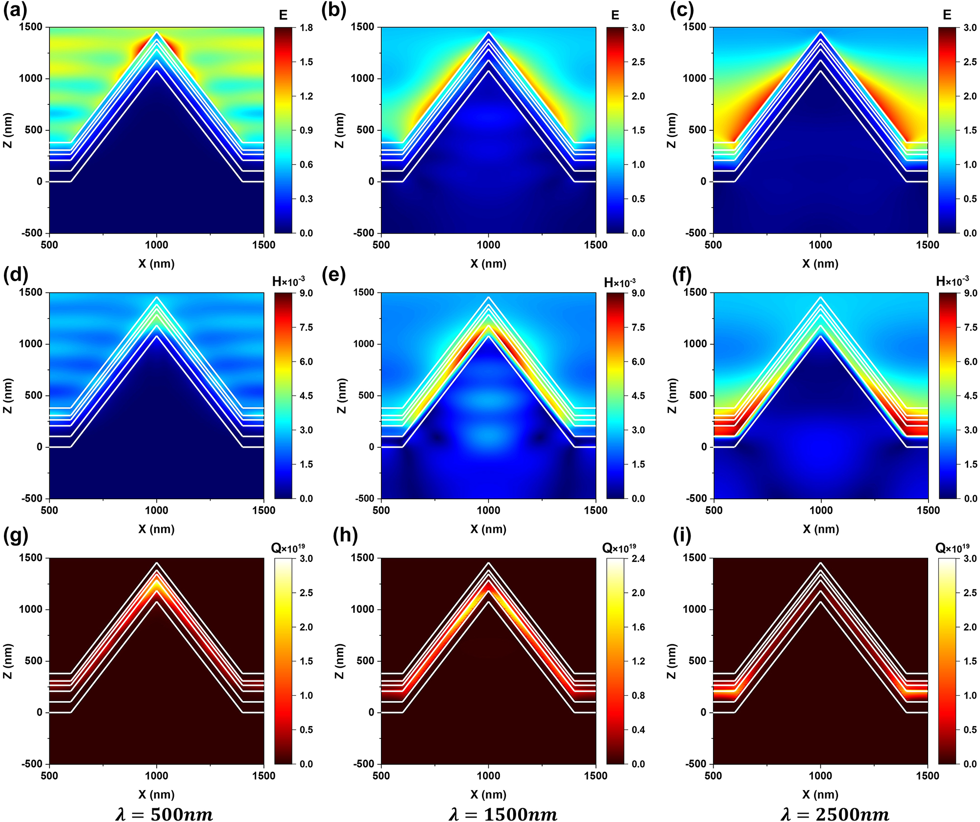
The contour plots represent the electric field intensity (a, b, c), magnetic field intensity (d, e, f) and the heat power density (g, h, i) at normal incidence for TM-polarized light with different incident wavelength.
For short wavelength around λ = 500 nm, it can be seen from Figure 4(a) that the top of the cone presents a strong electric field, which means that the plasma near-field coupling between the metal arrays is excited [44]. Therefore, most of the energy is dissipated at the top of the proposed absorber, as shown in Figure 4(g). At medium wavelength around λ = 1500 nm, the enhanced magnetic field is localized on the sidewall of the absorber as shown in Figure 4(e), which can be attributed to the excitation of magnetic polaritons (MPs). The MPs lead to high absorption of the energy by the sidewall as shown in Figure 4(h). Here, an inductor–capacitor (LC) circuit can be used to analyze MPs and the resonance wavelength can be predicted by
3 Fabrication
The predominant nanofabrication technologies are usually time-consuming and costly which result in the inability to efficiently fabricate nanostructures in large-area. To overcome the aforementioned drawbacks, a composite process of two easy-operated and efficient methods, colloidal lithography and magnetron sputtering, is integrated to obtain the proposed absorber.
The fabrication process employs the microspheres self-assembly technology, reactive ion etching (RIE-501, Jingshengweina Technology), and magnetron sputtering (MSP-300, Jingshengweina Technology), as illustrated in Figure 5. Firstly, the PI substrate is ultrasonically cleaned in ethanol for 20 min to enhance its hydrophilicity. The 10%wt polystyrene (PS) microspheres (1 μm) aqueous solution and equal volume ethanol mixture is then added to deionized water mixed with 50 μL 10%wt sodium dodecyl sulfate (SDS). The PS microspheres are self-assembled into a large-area and hexagonal close-packed monolayer on the water–air interface due to the surface tension and capillary force. This monolayer is transferred to the prepared PI substrate after 24 h of drying in the air.
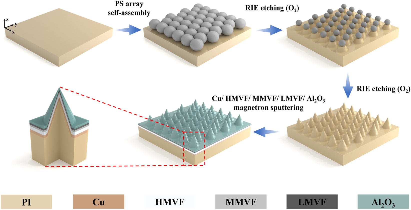
Schematic of the steps involved in the fabrication.
Secondly, with O2 RIE, both PS microspheres and PI substrate are etched effectively. The RIE are performed under a pressure of 2 Pa, an O2 gas flow rate of 20 SCCM and RF power of 50 W; the time of processes is set as 1500 s. So far, the tapered PI substrate is successfully prepared. Lastly, the five-layer thin film is deposited on the tapered PI substrate through the magnetron sputtering process and Table 2 presents the detailed parameters of the process. In detail, the metal filling factor f can be flexibly controlled by changing the Ar and O2 gas flow as well as the sputtering power. Consequently, a large-area (2 cm × 2 cm) absorber is efficiently fabricated.
Parameters of magnetron sputtering.
| Materials | Sputtering target | Gas flow/SCCM | Power | Time | |
|---|---|---|---|---|---|
| Ar | O2 | ||||
| Cu | Cu | 100 | – | DC: 150 W | 100 s |
| Zr–ZrO2 (HMVF) | Zr | 60 | 9 | RF: 610 W | 107 s |
| Zr–ZrO2 (MMVF) | Zr | 100 | 10 | RF: 600 W | 170 s |
| Zr–ZrO2 (LMVF) | Zr | 100 | 10 | RF: 575 W | 85 s |
| Al2O3 | Al2O3 | 100 | – | RF: 400 W | 800 s |
The scanning electron microscope (SEM) images of the prepared samples are characterized by the focused ion beam-scanning electron microscope (FIB-SEM, Auriga-4523, Zeiss). An ultrathin Pt layer is deposited on the surface to improve the conductivity of the samples. PS microspheres with a diameter of 1 μm formed a hexagonally close-packed monolayer on the 2 cm × 2 cm PI substrate, which act as a mask in the subsequent etching process, as represented in Figure 6(a) and (b). Figure 6(c) and (d) depict the prepared tapered PI substrate after the O2 RIE and ultrasonic cleaning processes. The height and the bottom diameters of the cones are approximately 1000 nm and 800 nm, respectively. The parameters of the cones can also be adjusted by the etching parameters. Then, five-layer cermet film is uniformly deposited on the sample, presenting a negligible change in the morphology of the sample, as shown in Figure 6(e) and (f).
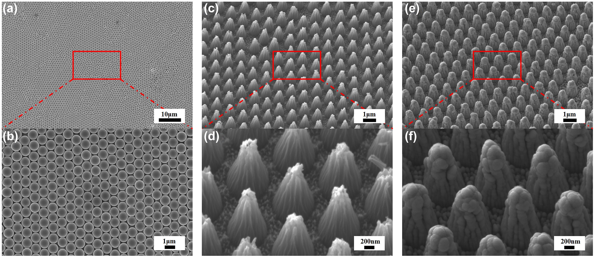
SEM diagram of the fabrication process. (a–b) SEM images of monolayer hexagonal PS microsphere arrays at 0° with different scale. (c–d) SEM images of tapered PI substrate at 30° with different scale. (e–f) SEM images of the proposed nano-cone absorber at 30° with different scale.
4 Experimental results
The transmittance is close to zero since the thickness of the bottom copper layer is much greater than the penetration depth. Therefore, the measured absorbance is calculated as A = 1 − R. The absorption performance of sample is tested by measuring the reflection spectrum using a spectrophotometer (UV-3101 PC, Shimadzu) and absorption performance of the oblique incidence is tested from 10° to 60° using UV-VIS-NIR spectrophotometer (Lambda950, Wavetest) equipped with the absolute specular reflectance accessory.
Figure 7(a) presents the comparison between the simulated and measured absorbance from 300 nm to 3000 nm at normal incidence (0°) for unpolarized light and the inset is a photograph of the prepared centimeter-scale (2 cm × 2 cm) sample which appears black, indicating that it has good absorption performance in the visible regime. Figure 7(b) presents the measured absorbance at different oblique incident angles varying from 10° to 60° in steps of 10°. It can be concluded that the measured results correspond well with the simulated results, based on Figure 7(a) and the comparison between Figures 3(b) and 7(b). Surprisingly, the measured absorbance the measured absorbance shows better angular tolerance than the simulated results. This is mainly due to the presence of some metal nanoparticles on the sample surface during magnetron sputtering, which excites the localized surface plasmon [46, 47].
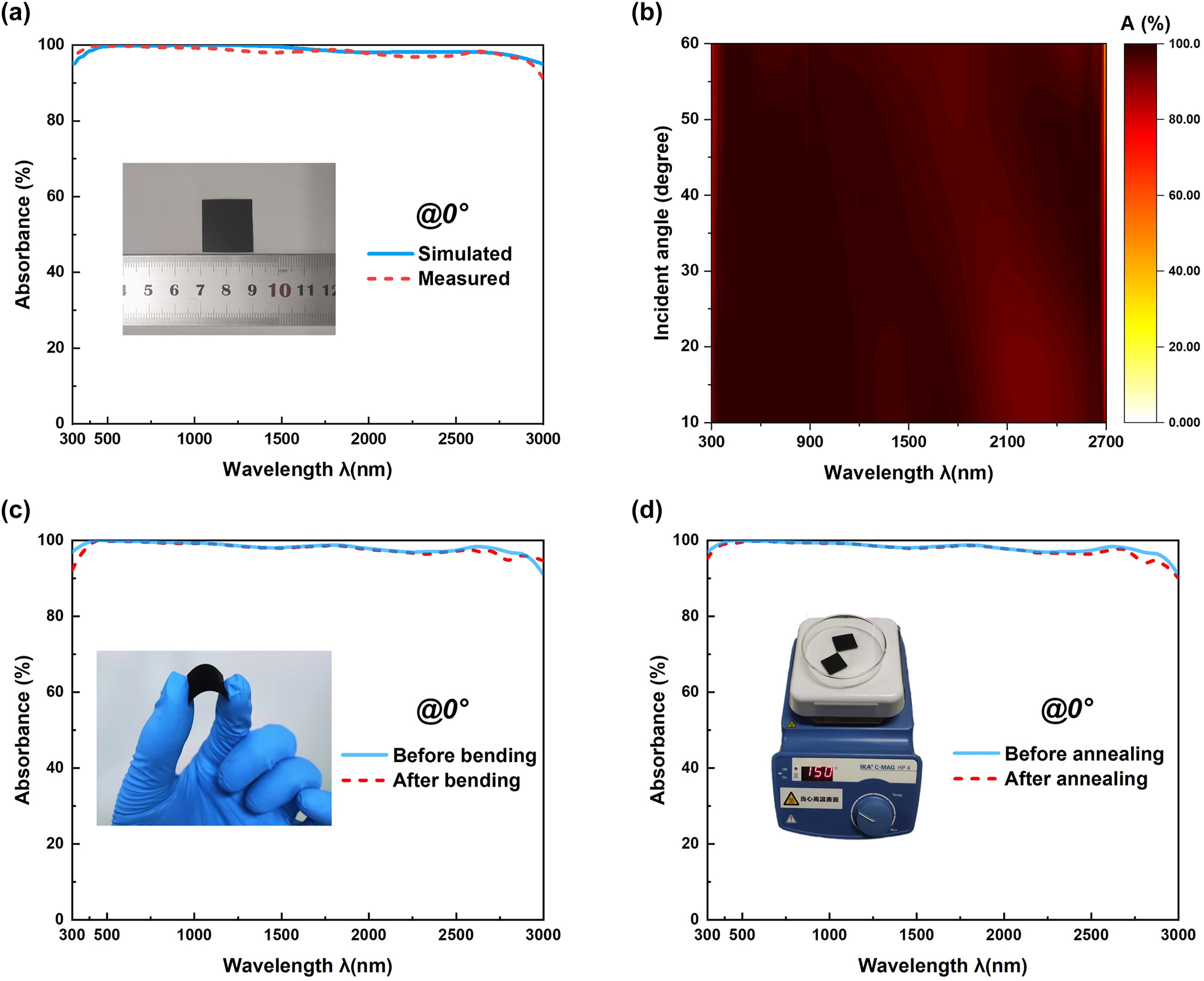
Test results of the sample's absorption performance. (a) The comparison between calculated and measured absorbance at normal incident angle for unpolarized light. (b) Measured absorption spectrum of prepared sample at different incident angles varying from 10° to 60° in 10° steps for unpolarized light. (c) Measured absorption spectrum before and after 100 times of bending tests at normal incident angle for unpolarized light. (d) Measured absorption spectrum before and after 6 h of 150 °C annealing tests at normal incident angle for unpolarized light.
Additionally, due to the flexible PI substrate which has tolerance to high temperature, the prepared absorber shows good bending resistance and heat resistance. Additionally, the absorption spectrum of the prepared sample is compared before and after the 100 iterations of bending tests and the inset is the photography of the bending test, as shown in Figure 7(c). Furthermore, by using hot plates (C-MAG HP 4, IKA) the prepared absorber was heated to 150 °C for 6 h. And the absorption spectrum of the prepared sample is compared before and after annealing test and the inset is the photography of the annealing test, as represented in Figure 7(d). There is almost no difference in the absorption spectrum at normal incidence as Figure 7(c) and (d) reveals, indicating that the prepared absorber has great bending resistance and heat resistance.
5 Conclusions
In summary, this work proposes a design of broadband planar multi-cermet absorber made of Cu/Zr–ZrO2 (HMVF)/Zr–ZrO2 (MMVF)/Zr–ZrO2 (LMVF)/Al2O3. Then we present a simple yet generalized design for ultra-broadband metamaterial absorber which improves the absorption performance greatly, based on the planar one. By using the colloidal lithography method and magnetron sputtering composite process the centimeter-scale (2 cm × 2 cm) absorber is efficiently fabricated. The proposed metamaterial absorber is composed of polyimide (PI) substrate with nano-cone array and multi-cermet films. Based on the optical interference of the multi-cermet films, plasma near-field coupling and excited magnetic resonance of light trapping structures, the average absorbance of the proposed absorber is more than 98.7% (experiment result: 98.1%) from 300 to 3000 nm. Using spectrophotometer to test the fabricated absorber, it can be observed that the measured results correspond well with the simulated results and exhibit better angular tolerance. Additionally, owing to the use of flexible PI substrate, the proposed absorber also shows good bending resistance and heat resistance, which reflects its potential engineering value.
Funding source: National Natural Science Foundation of China
Award Identifier / Grant number: No.62035016
-
Author contributions: All the authors have accepted responsibility for the entire content of this submitted manuscript and approved submission.
-
Research funding: This work was funded by the National Natural Science Foundation of China (Grants No.62035016).
-
Conflict of interest statement: The authors declare no conflicts of interest regarding this article.
References
[1] H. Wang and L. Wang, “Perfect selective metamaterial solar absorbers,” Opt. Express, vol. 21, no. 106, pp. A1078–A1093, 2013. https://doi.org/10.1364/oe.21.0a1078.Search in Google Scholar PubMed
[2] M. Gao, L. Zhu, C. K. Peh, and G. W. Ho, “Solar absorber material and system designs for photothermal water vaporization towards clean water and energy production,” Energy Environ. Sci., vol. 12, no. 3, pp. 841–864, 2019. https://doi.org/10.1039/c8ee01146j.Search in Google Scholar
[3] A. K. Azad, W. J. Kort-Kamp, M. Sykora, et al.., “Metasurface broadband solar absorber,” Sci. Rep., vol. 6, no. 1, pp. 1–6, 2016. https://doi.org/10.1038/srep20347.Search in Google Scholar PubMed PubMed Central
[4] K. Chi, L. Yang, Z. Liu, P. Q. Gao, J. Ye, and S. He, “Large-scale nanostructured low-temperature solar selective absorber,” Opt. Lett., vol. 42, no. 10, pp. 1891–1894, 2017. https://doi.org/10.1364/ol.42.001891.Search in Google Scholar
[5] Z. Zhang, Y. Mo, H. Wang, Y. Zhao, and S. Jiang, “High-performance and cost-effective absorber for visible and near-infrared spectrum based on a spherical multilayered dielectric–metal structure,” Appl. Opt., vol. 58, no. 16, pp. 4467–4473, 2019. https://doi.org/10.1364/ao.58.004467.Search in Google Scholar PubMed
[6] S. Behera and J. Joseph, “Plasmonic metamaterial based unified broadband absorber/near infrared emitter for thermophotovoltaic system based on hexagonally packed tungsten doughnuts,” J. Appl. Phys., vol. 122, no. 19, p. 193104, 2017. https://doi.org/10.1063/1.5003054.Search in Google Scholar
[7] F. Ding, J. Dai, Y. Chen, J. Zhu, Y. Jin, and S. I. Bozhevolnyi, “Broadband near-infrared metamaterial absorbers utilizing highly lossy metals,” Sci. Rep., vol. 6, no. 1, pp. 1–9, 2016, https://doi.org/10.1038/srep39445.Search in Google Scholar PubMed PubMed Central
[8] C. Lee, W. Yang, and R. G. Parr, “Development of the Colle-Salvetti correlation-energy formula into a functional of the electron density,” Phys. Rev. B, vol. 37, no. 2, p. 785, 1988. https://doi.org/10.1103/physrevb.37.785.Search in Google Scholar PubMed
[9] T. A. Chen, M. J. Yub, Y. J. Lu, and T. J. Yen, “Ultra-broadband, lithography-free, omnidirectional, and polarization-insensitive perfect absorber,” Sci. Rep., vol. 11, no. 1, pp. 1–7, 2021. https://doi.org/10.1038/s41598-021-84889-0.Search in Google Scholar PubMed PubMed Central
[10] D. Wen, F. Yue, G. Li, et al.., “Helicity multiplexed broadband metasurface holograms,” Nat. Commun., vol. 6, no. 1, pp. 1–7, 2015. https://doi.org/10.1038/ncomms9241.Search in Google Scholar PubMed PubMed Central
[11] X. Liu, T. Starr, A. F. Starr, and W. J. Padilla, “Infrared spatial and frequency selective metamaterial with near-unity absorbance,” Phys. Rev. Lett., vol. 104, no. 20, p. 207403, 2010. https://doi.org/10.1103/physrevlett.104.207403.Search in Google Scholar PubMed
[12] M. ElKabbash, K. V. Sreekanth, Y. Alapan, et al.., “Hydrogen sensing using thin-film perfect light absorber,” ACS Photonics, vol. 6, no. 8, pp. 1889–1894, 2019. https://doi.org/10.1021/acsphotonics.9b00764.Search in Google Scholar
[13] A. Tittl, A. K. U. Michel, M. Schäferling, et al.., “A switchable mid-infrared plasmonic perfect absorber with multispectral thermal imaging capability,” Adv. Mater., vol. 27, no. 31, pp. 4597–4603, 2015. https://doi.org/10.1002/adma.201502023.Search in Google Scholar PubMed
[14] D. Wu, Y. Liu, R. Li, et al.., “Infrared perfect ultra-narrow band absorber as plasmonic sensor,” Nanoscale Res. Lett., vol. 11, no. 1, pp. 1–9, 2016. https://doi.org/10.1186/s11671-016-1705-1.Search in Google Scholar PubMed PubMed Central
[15] Y. Liang, W. Cui, L. Li, Z. Yu, W. Peng, and T. Xu, “Large‐scale plasmonic nanodisk structures for a high sensitivity biosensing platform fabricated by transfer nanoprinting,” Adv. Opt. Mater., vol. 7, no. 7, p. 1801269, 2019. https://doi.org/10.1002/adom.201801269.Search in Google Scholar
[16] W. Li and J. Valentine, “Metamaterial perfect absorber based hot electron photodetection,” Nano Lett., vol. 14, no. 6, pp. 3510–3514, 2014. https://doi.org/10.1021/nl501090w.Search in Google Scholar PubMed
[17] Y. Zhai, G. Chen, J. Ji, et al.., “Large-scale, broadband absorber based on three-dimensional aluminum nanospike arrays substrate for surface plasmon induced hot electrons photodetection,” Nanotechnology, vol. 30, no. 37, p. 375201, 2019. https://doi.org/10.1088/1361-6528/ab2158.Search in Google Scholar PubMed
[18] L. Zhou, C. Zhang, L. Li, et al.., “Nanobowls-assisted broadband absorber for unbiased Si-based infrared photodetection,” Opt. Express, vol. 29, no. 10, pp. 15505–15516, 2021. https://doi.org/10.1364/oe.423897.Search in Google Scholar
[19] L. Feng, P. Huo, Y. Liang, and T. Xu, “Photonic metamaterial absorbers: morphology engineering and interdisciplinary applications,” Adv. Mater., vol. 32, no. 27, p. 1903787, 2020. https://doi.org/10.1002/adma.201903787.Search in Google Scholar PubMed
[20] Z. Yong, S. Zhang, C. Gong, and S. He, “Narrow band perfect absorber for maximum localized magnetic and electric field enhancement and sensing applications,” Sci. Rep., vol. 6, no. 1, pp. 1–7, 2016. https://doi.org/10.1038/srep24063.Search in Google Scholar PubMed PubMed Central
[21] Z. Li, S. Butun, and K. Aydin, “Large-area, lithography-free super absorbers and color filters at visible frequencies using ultrathin metallic films,” ACS Photonics, vol. 2, no. 2, pp. 183–188, 2015. https://doi.org/10.1021/ph500410u.Search in Google Scholar
[22] A. Moreau, C. Ciracì, J. J. Mock, et al.., “Controlled-reflectance surfaces with film-coupled colloidal nanoantennas,” Nature, vol. 492, no. 7427, pp. 86–89, 2012. https://doi.org/10.1038/nature11615.Search in Google Scholar PubMed PubMed Central
[23] P. Mandal and C. N. Rao, “Period-and cavity-depth-dependent plasmonic metamaterial perfect absorber at visible frequency: design rule,” J. Nanophotonics, vol. 11, no. 3, p. 036003, 2017. https://doi.org/10.1117/1.jnp.11.036003.Search in Google Scholar
[24] J. Hao, J. Wang, X. Liu, W. J. Padilla, L. Zhou, and M. Qiu, “High performance optical absorber based on a plasmonic metamaterial,” Appl. Phys. Lett., vol. 96, no. 25, p. 251104, 2010. https://doi.org/10.1063/1.3442904.Search in Google Scholar
[25] H. K. Raut, V. A. Ganesh, A. S. Nair, and S. Ramakrishna, “Anti-reflective coatings: a critical, in-depth review,” Energy Environ. Sci., vol. 4, no. 10, pp. 3779–3804, 2011. https://doi.org/10.1039/c1ee01297e.Search in Google Scholar
[26] A. Ghobadi, H. Hajian, B. Butun, and E. Ozbay, “Strong light–matter interaction in lithography-free planar metamaterial perfect absorbers,” ACS Photonics, vol. 5, no. 11, pp. 4203–4221, 2018. https://doi.org/10.1021/acsphotonics.8b00872.Search in Google Scholar
[27] Z. Li, E. Palacios, S. Butun, H. Kocer, and K. Aydin, “Omnidirectional, broadband light absorption using large-area, ultrathin lossy metallic film coatings,” Sci. Rep., vol. 5, no. 1, pp. 1–8, 2015. https://doi.org/10.1038/srep15137.Search in Google Scholar PubMed PubMed Central
[28] F. Teng, N. Li, L. Liu, D. Xu, D. Xiao, and N. Lu, “Fabrication of ordered Si nanopillar arrays for ultralow reflectivity,” RSC Adv., vol. 6, no. 19, pp. 15803–15807, 2016. https://doi.org/10.1039/c5ra25484a.Search in Google Scholar
[29] L. Zhou, Y. Tan, J. Wang, et al.., “3D self-assembly of aluminium nanoparticles for plasmon-enhanced solar desalination,” Nat. Photonics, vol. 10, no. 6, pp. 393–398, 2016. https://doi.org/10.1038/nphoton.2016.75.Search in Google Scholar
[30] Y. Liu, J. Qiu, J. Zhao, and L. Liu, “General design method of ultra-broadband perfect absorbers based on magnetic polaritons,” Opt. Express, vol. 25, no. 20, pp. A980–A989, 2017. https://doi.org/10.1364/oe.25.00a980.Search in Google Scholar PubMed
[31] A. Ghobadi, H. Hajian, M. Gokbayrak, B. Butun, and E. Ozbay, “Bismuth-based metamaterials: from narrowband reflective color filter to extremely broadband near perfect absorber,” Nanophotonics, vol. 8, no. 5, pp. 823–832, 2019. https://doi.org/10.1515/nanoph-2018-0217.Search in Google Scholar
[32] W. Yu, Y. Lu, X. Chen, et al.., “Large‐area, broadband, wide‐angle plasmonic metasurface absorber for midwavelength infrared atmospheric transparency window,” Adv. Opt. Mater., vol. 7, no. 20, p. 1900841, 2019. https://doi.org/10.1002/adom.201900841.Search in Google Scholar
[33] W. Hou, F. Yang, Z. Chen, J. Dong, and S. Jiang, “Wide-angle and broadband solar absorber made using highly efficient large-area fabrication strategy,” Opt. Express, vol. 30, no. 3, pp. 4424–4433, 2022. https://doi.org/10.1364/oe.451411.Search in Google Scholar
[34] Q. C. Zhang, “Optimizing analysis of W-AlN cermet solar absorbing coatings,” J. Phys. D: Appl. Phys., vol. 34, no. 21, p. 3113, 2001. https://doi.org/10.1088/0022-3727/34/21/303.Search in Google Scholar
[35] M. R. Nejati, V. Fathollahi, and M. K. Asadi, “Computer simulation of the optical properties of high-temperature cermet solar selective coatings,” Sol. Energy, vol. 78, no. 2, pp. 235–241, 2005. https://doi.org/10.1016/j.solener.2004.09.024.Search in Google Scholar
[36] P. Sheng, “Theory for the dielectric function of granular composite media,” Phys. Rev. Lett., vol. 45, no. 1, p. 60, 1980. https://doi.org/10.1103/physrevlett.45.60.Search in Google Scholar
[37] M. R. Querry, Optical Constants of Minerals and Other Materials from the Millimeter to the Ultraviolet, Chemical Research, Development & Engineering Center, US Army Armament Munitions Chemical Command, 1998.Search in Google Scholar
[38] D. L. Wood and K. Nassau, “Refractive index of cubic zirconia stabilized with yttria,” Appl. Opt., vol. 21, no. 16, pp. 2978–2981, 1982. https://doi.org/10.1364/ao.21.002978.Search in Google Scholar PubMed
[39] J. Wang, Z. Ren, Y. Luo, et al.., “High-performance spectrally selective absorber using the ZrB2-based all-ceramic coatings,” ACS Appl. Mater. Interfaces, vol. 13, no. 34, pp. 40522–40530, 2021. https://doi.org/10.1021/acsami.1c08947.Search in Google Scholar PubMed
[40] A. D. Rakić, A. B. Djurišić, J. M. Elazar, and M. L. Majewski, “Optical properties of metallic films for vertical-cavity optoelectronic devices,” Appl. Opt., vol. 37, no. 22, pp. 5271–5283, 1998. https://doi.org/10.1364/ao.37.005271.Search in Google Scholar PubMed
[41] R. Boidin, T. Halenkovič, V. Nazabal, L. Beneš, and P. Němec, “Pulsed laser deposited alumina thin films,” Ceram. Int., vol. 42, no. 1, pp. 1177–1182, 2016. https://doi.org/10.1016/j.ceramint.2015.09.048.Search in Google Scholar
[42] M. J. Tommalieh and A. M. Zihlif, “Optical properties of polyimide/silica nanocomposite,” Phys. B Condens. Matter, vol. 405, no. 23, pp. 4750–4754, 2010. https://doi.org/10.1016/j.physb.2010.08.070.Search in Google Scholar
[43] Z. M. Zhang, G. Lefever-Button, and F. R. Powell, “Infrared refractive index and extinction coefficient of polyimide films,” Int. J. Thermophys., vol. 19, no. 3, pp. 905–916, 1998. https://doi.org/10.1023/a:1022655309574.10.1023/A:1022655309574Search in Google Scholar
[44] Y. Cheng, M. Xiong, M. Chen, et al.., “Numerical study of ultra-broadband metamaterial perfect absorber based on four-corner star array,” Nanomaterials, vol. 11, no. 9, p. 2172, 2021. https://doi.org/10.3390/nano11092172.Search in Google Scholar PubMed PubMed Central
[45] B. J. Lee, L. P. Wang, and Z. M. Zhang, “Coherent thermal emission by excitation of magnetic polaritons between periodic strips and a metallic film,” Opt. Express, vol. 16, no. 15, pp. 11328–11336, 2008. https://doi.org/10.1364/oe.16.011328.Search in Google Scholar PubMed
[46] L. Zhou, Y. Tan, D. Ji, et al.., “Self-assembly of highly efficient, broadband plasmonic absorbers for solar steam generation,” Sci. Adv., vol. 2, no. 4, p. e1501227, 2016. https://doi.org/10.1126/sciadv.1501227.Search in Google Scholar PubMed PubMed Central
[47] G. Hou, Z. Wang, Z. Lu, H. Song, J. Xu, and K. Chen, “Enhanced broadband plasmonic absorbers with tunable light management on flexible tapered metasurface,” ACS Appl. Mater. Interfaces, vol. 12, no. 50, pp. 56178–56185, 2020. https://doi.org/10.1021/acsami.0c16189.Search in Google Scholar PubMed
Supplementary Material
This article contains supplementary material (https://doi.org/10.1515/nanoph-2023-0021).
© 2023 the author(s), published by De Gruyter, Berlin/Boston
This work is licensed under the Creative Commons Attribution 4.0 International License.
Articles in the same Issue
- Frontmatter
- Editorial
- Special issue: Metamaterials and plasmonics in Asia, a tribute to Byoungho Lee
- Memorandum
- In memory of Prof. Byoungho Lee
- Reviews
- Advances and applications on non-Hermitian topological photonics
- Topological phases and non-Hermitian topology in photonic artificial microstructures
- Recent advanced applications of metasurfaces in multi-dimensions
- Recent advances in oblique plane microscopy
- Research Articles
- A symmetry-protected exceptional ring in a photonic crystal with negative index media
- Highly angle-sensitive and efficient optical metasurfaces with broken mirror symmetry
- Multilayer all-polymer metasurface stacked on optical fiber via sequential micro-punching process
- Inverse design of high-NA metalens for maskless lithography
- Deterministic approach to design passive anomalous-diffraction metasurfaces with nearly 100% efficiency
- Metasurface spatial filters for multiple harmonic signals
- Multiple symmetry protected BIC lines in two dimensional synthetic parameter space
- Deep-learning-assisted reconfigurable metasurface antenna for real-time holographic beam steering
- On-chip integration of metasurface-doublet for optical phased array with enhanced beam steering
- Multi-frequency amplitude-programmable metasurface for multi-channel electromagnetic controls
- Broadband absorber with dispersive metamaterials
- Visible-mid infrared ultra-broadband and wide-angle metamaterial perfect absorber based on cermet films with nano-cone structure
- Vertical photon sorting by stacking silicon and germanium nanopillars for broadband absorbers
- Directive emission from polymeric fluorophore with epsilon-near-zero squaraine molecular film
- Chiral-magic angle of nanoimprint meta-device
- Fluorescence engineering in metamaterial-assisted super-resolution localization microscope
- Nano-shaping of chiral photons
- Design principles for electrically driven Luttinger liquid-fed plasmonic nanoantennas
- Ultrafast strong-field terahertz nonlinear nanometasurfaces
- Reconfigurable anomalous reflectors with stretchable elastic substrates at 140 GHz band
- Polarization-independent isotropic metasurface with high refractive index, low reflectance, and high transmittance in the 0.3-THz band
- Terahertz nanofuse by a single nanowire-combined nanoantenna
- Electrically tunable THz graphene metasurface wave retarders
- Ultra-thin grating coupler for guided exciton-polaritons in WS2 multilayers
- Reflection of two-dimensional surface polaritons by metallic nano-plates on atomically thin crystals
- A deep neural network for general scattering matrix
- Engineering isospectrality in multidimensional photonic systems
- Heterogeneously integrated light emitting diodes and photodetectors in the metal-insulator-metal waveguide platform
- DNA origami-designed 3D phononic crystals
- All-dielectric carpet cloaks with three-dimensional anisotropy control