
Design principles for electrically driven Luttinger liquid-fed plasmonic nanoantennas
-
Eun Su Jeon
 ,
YoonYeong Ko
and
SeokJae Yoo
,
YoonYeong Ko
and
SeokJae Yoo


Abstract
Electrons injected into one-dimensional (1D) metals are efficiently converted into infrared plasmons because the unique property of the Luttinger liquid, a strongly correlated electronic matter in one-dimensional (1D) metals, prohibits excitations of other quasiparticles. Using the Luttinger liquid behavior, the electrically driven 1D metals can be used as a feed for optical nanoantennas. Nanoantennas can couple the 1D Luttinger liquid plasmons in the feed to the radiating photons in free space. In this work, we suggest design principles for the 1D metallic Luttinger liquid feed and the nanoantennas to obtain high injection and radiation efficiencies, respectively. We expect that our work can promote experimental efforts to realize electrically driven Luttinger liquid-fed nanoantennas and efficient infrared light sources.
1 Introduction
Current research for a plasmonic nanoantenna, an optical analog of a radio antenna, aims at a bidirectional operation of antennas; conversion of photons into electrons (i.e. a receiver) and its reverse conversion (i.e. a transmitter). While the receiving operation can be achieved straightforwardly using semiconductor photodetectors, the transmitting process requires an efficient scheme to drive plasmonic nanoantenna electrically. One of the promising antenna driving schemes is photon emission in the inelastic tunneling process through plasmonic metal nanogaps [1–8]. Some of the electrons tunnel inelastically through the electrically biased nanogap, while most of them elastically tunnel and are transported as the direct current (DC). The inelastic tunneling results in a temporal fluctuation of an electrical current, which is called the quantum shot noise current [2, 3, 5, 8], [9], [10]. The temporal current fluctuations provide photon emission at extremely low efficiency (one photon per ∼105 tunnel electrons) [2, 11] although resonant plasmonic antenna can provide additional enhancement of the photon emission efficiency. Another driving scheme is to use a light-emitting semiconductor feed [12, 13]. Despite its success in visible and near-infrared frequencies, narrow-gap semiconductors become inefficient in mid-infrared (MIR) band emissions because the nonradiative Auger process is dominant [14–16].
Recently, we have proposed that the Luttinger liquid behavior of electrons confined in one-dimensional (1D) paramagnetic metals can provide efficient infrared photon emission when electrons are injected elastically into the 1D metals [17]. In 1D metals, electron–electron interaction becomes dominant, and electrons behave as a strongly correlated electronic liquid, rather than quasi-free particles. Therefore, 1D electronic behavior becomes completely different from higher dimensional metals. The elementary excitation of the Luttinger liquid is plasmons and spinons, which are collective oscillations of charges and spins, respectively. Therefore, in the Luttinger liquid, other excitations, e.g. phonons and free electrons, are fundamentally forbidden. This extraordinary property results in the highly efficient injection of electrons into the Luttinger liquid. It has also been proposed that the plasmonic nanoantenna, e.g. gold nanorods, nearby can convert the electrically excited Luttinger liquid plasmons into the far-field radiation. The sequential processes of the efficient plasmon excitation and its coupling to the far field can provide a novel route toward electrically driven nanoantennas and efficient infrared lighting.
In this work, we present design principles for plasmonic nanoantennas with the electrically driven Luttinger liquid feed. First of all, we show that electron tunneling through a semiconductor contact can significantly enhance the electron injection efficiency of the Luttinger liquid plasmon. Secondly, we provide design principles for nanoantenna to enhance the Luttinger liquid plasmon-to-radiating photon conversion efficiency. We also suggest a grating nanoantenna design for the practical realization of infrared lighting. We expect our design principles can promote experimental efforts to realize the electrically driven Luttinger liquid-fed plasmonic nanoantennas.
2 Results
The transmitting operation of the Luttinger liquid-fed nanoantenna follows two steps (Figure 1a): (i) electrons are injected into 1D metals, and they efficiently excite the Luttinger liquid plasmons and spinons. (ii) Nanoantenna helps the electrically excited Luttinger liquid plasmons to couple with the radiating photons. Since the plasmon momentum (red line in Figure 1b) is much larger than the photon momentum (black line in Figure 1c) for a given frequency ω, the nanoantenna coupling is needed to radiate the photon in the far field. In this work, we provide design principles for the Luttinger liquid feed and the nanoantenna to enhance the injection efficiency η inj (step [i]) and the radiation efficiency η rad (step [ii]). In this work, we choose metallic single-walled carbon nanotubes (SWNTs) as the 1D metallic system that hosts the Luttinger liquid. Unique features of the Luttinger liquid have been demonstrated in many experiments including transport [18–20], infrared near-field microscopy [20–22], and electron tunneling-plasmon correlation experiment [20]. The linear dispersion (e.g. Figure 1b), the requirement of the paramagnetic 1D metal to host the Luttinger liquid [23], is also robust up to the near-infrared region (∼1 eV) [24, 25]. Although we choose SWNTs as the Luttinger liquid feed material in this work, our antenna design principle does not restrict to SWNTs. Our approach can be applied to any 1D metals, e.g. gold atom chains, conducting polymers [26], the mirror-twin boundary of 2D TMDs [27], and twisted WTe2 [28]. The Luttinger liquid interaction parameter g = v F /v p , the modification of the plasmon velocity v p compared to the Fermi velocity v F by the strong electron–electron interaction in 1D metals, determines the electrical and optical behaviors of the Luttinger liquid; g < 1, g = 1, g > 1 correspond to repulsive, vanishing, and attractive interactions, respectively [29]. For example, metallic single-walled carbon nanotubes (SWNT) have g ∼ 0.3.
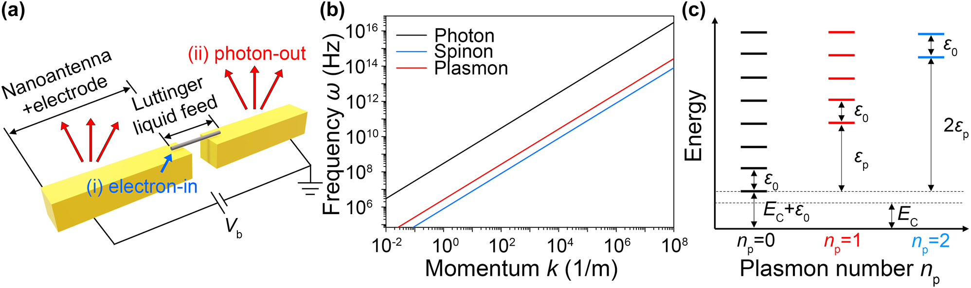
The Luttinger liquid characteristics. (a) Working principle of the electrically driven Luttinger liquid-fed nanoantenna (each step is summarized by blue and red color). The 1D metal at a gap between two gold nanoantennas works as the Luttinger liquid feed when electrons are injected from the gold nanoantenna with a bias voltage V b . (b) The linear dispersion of the Luttinger liquid plasmons (red line: ω = v p k = (v F /g)k), the non-interacting fermi electrons (blue line: ω = v F k), and the radiating photons (black line: ω = ck) with the frequency ω, the speed of light c, the plasmon velocity v p , the fermi velocity v F , the momentum k, the Luttinger liquid interaction parameter g, and the speed of light c. The dispersion is plotted in a log-log scale with typical parameters of metallic single-walled carbon nanotubes: g = 0.3 and v F = 8 × 10⁵ m/s. (c) The energy spectrum of the Luttinger liquid quantum states is composed of plasmons and spinons. Quantum numbers n p and n 0 define the energy levels of the plasmon and spinon states (E C : the Coulomb blockade energy, ε 0: the spinon energy, and ε p = ε 0/g: the plasmon energy).
2.1 Tailoring electron injection efficiency
Once electrons are injected into the Luttinger liquid, all the injected electrons are converted into plasmons and spinons because they are the elementary excitation. Injected electrons cannot remain as quasi-free electrons in direct current (DC) because quasiparticles are forbidden except for the plasmons and spinons in the Luttinger liquid. Other quasiparticle excitations, which are nonradiative loss channels, are fundamentally forbidden in the Luttinger liquid. This elementary excitation property of the Luttinger liquid is a key to efficient infrared photon emission; the injected electrons get a high chance of conversion into plasmons that can couple to radiating photons. In the Luttinger liquid, there are many quantum states of plasmon and spinon excitations that are defined by plasmon quantum number n
p
and spinon quantum number n
0 (n
p
, n
0 ≥ 0) as depicted in Figure 1c. Among the quantum states, the dipolar plasmon states (n
p
= 1) alone are radiative, while the other plasmon states (n
p
≠ 1) and spinon excitations are nonradiative. Therefore, we define the injection efficiency
First of all, the excitation strength of the dipolar plasmon depends on the location of the electron injection. Given 1D metal of length l
LL
, dipolar plasmon strength is proportional to
The length of the 1D metal l
LL
and the Luttinger liquid interaction parameter g affect the injection property. However, l
LL
has a constraint imposed by the photon emission wavelength
For the resonant length l
LL
, we investigate the effect of l
LL
and g on the injection efficiency η
inj. The energies of the spinon and plasmon states are determined by
whose peaks appear at the energy
where the Heaviside theta step function θ is defined by θ(x − a) = 1 and 0 for x > a and x ≤ a, respectively. Since the dipolar plasmons alone contribute to the radiation, we define the power injected into the dipolar plasmons (n
p
= 1) excluding spinon excitations in the form,
where the normalized dipole plasmon current
We plot η
inj(ε) for varying the Luttinger liquid interaction parameter g. Since the dipole plasmon states (n
p
= 1) alone contribute to the radiation, η
inj starts to increase after the lowest energy of the dipole plasmons ε
10 = ε
p
+ ε
0/2 + E
C
= ε
0(3g
2 + 8g + 1)/(8g
2). Once the electron injection occurs after the Coulomb blockade energy E
C
(the boundary between the dark region and the bright region in Figure 2), the injection efficiency maximum η
inj(ε
max) of 17.1% appears at ε
max = 360 meV for the smallest g = 0.15, while η
inj(ε
max) decreases to 11.2% for the largest g = 0.5. As g decreases, ε
max becomes larger, while the maximum efficiency η
inj(ε
max) increases. This behavior of better η
inj(ε
max) for small g results from two contributions; (i) the dipole plasmon power
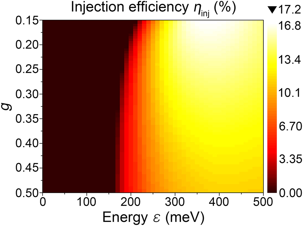
Tailoring the electron injection efficiency η inj(ε) by the Luttinger liquid interaction parameter g. The electrons are injected at the end of the 1D metal (x = 0 or l LL ).
In addition, the output power of our antenna can be improved by a small g. The 1D metal of small g also possesses a larger dipole plasmon current,
The smallness of g provides an additional practical advantage in device fabrication. The resonant 1D metal length l
LL
becomes longer for reduced g due to the constraint,
Before concluding this section, we need to mention the experimental way to reduce the Luttinger liquid interaction parameter g. g varies by the 1D metal species and its dielectric environment. For example, metallic SWNTs follow the logarithmic diameter scaling of g [17, 21, 22]; thinner SWNT has smaller g (e.g. g ∼ 0.29 and 0.36 for diameters of 0.5 nm and 2.0 nm, respectively.) Smaller background permittivity also makes g smaller [17, 21]. Recently, extremely small g ∼ 0.14 has also been reported in the 1D metal phase in twisted WTe2 [28].
It is also noteworthy that other factors can affect the electrical property of the Luttinger liquid feed. First of all, the tunneling current in the 1D metal may experience exponential decrease according to the tunneling barrier characteristics, e.g. barrier width and height [32], affecting the resultant injection efficiency. Secondly, we assume the 1D metal feed shorter than 40 nm in our work, but longer feed can suffer from the electron–phonon scattering [33].
To summarize the design principle for high injection efficiency, the following conditions should be met:
Electrons should be injected at the end of the 1D metals rather than the middle because tunneling into the middle suppresses the dipolar plasmons.
Length of the 1D metals (l LL ) is determined by the target wavelength of photon emission (
Smaller Luttinger liquid interaction parameter g leads to higher injection efficiency η inj and the dipole current strength I 0.
The bias energy eV b = ε max to maximize η inj can be found near the energy of the lowest quadrupole plasmon (n p = 2 and n 0 = 0), ε 20 = ε 0(3g 2 + 16g + 1)/(8g 2) if g is small enough.
2.2 Tailoring photon radiation efficiency
2.2.1 Calculating the radiation efficiency
To calculate the optical performance of the Luttinger liquid-fed nanoantennas, we include the quantum mechanical properties of the Luttinger liquid in the classical electromagnetic calculation. Resulting from the quantum mechanical electron–electron interaction in 1D metals, the Luttinger liquid has a linear dispersion,
where the complex plasmon momentum and the free space photon momentum are given by
which works well for a narrow spectral band (λ
0).
To characterize the optical radiation process, i.e. the plasmon-to-photon conversion, in step (ii), we need to calculate the radiation efficiency,
where the total input power P
in consumed by the whole antenna system is given by a sum of P
rad and the absorbed powers in the Luttinger liquid feed (P
Ω,LL
) and in the nanoantenna (P
Ω,a
). In the last line of Eq. (7), we define the radiation resistance
2.2.2 Antenna analysis – the antenna circuit model
Although Eq. (7) reveals which factors can be improved for better radiation efficiency η
rad, i.e. large R
rad, small R
Ω, and large |I
a
|/|I
LL
|, it is not straightforward to predict the current strength ratio |I
a
|/|I
LL
|. An antenna circuit model in Figure 3b is useful to gain insight to enhance |I
a
|/|I
LL
|. We proposed an antenna circuit model composed of two RLC circuits (i.e. the 1D metal and the nanoantenna) connected by the interaction capacitor (C
int), and demonstrated that the model can describe the radiation features of the numerical simulations [17]. R
a(LL), L
a(LL), and C
a(LL) are the lumped circuit parameters of the antenna (the Luttinger liquid feed). Note that the lumped resistance R
a(LL) includes R
rad and R
Ω. The circuit model provides the current strength ratio
Tailoring the photon radiation efficiency. (a) Schematic drawing of the Luttinger liquid-fed nanoantennas (w: the antenna thickness, d: the gap distance, l a : the nanoantenna length, l LL = d + 2l T : the Luttinger liquid feed length, l T : the overlap length, t: tunneling gap distance). (b) The antenna circuit model with the lumped RLC circuits for the feed and the nanoantenna connected by the interaction capacitor C int. The whole circuit is driven by the current source I 0 excited by the electron injection. Changes in the radiation efficiency η rad(λ 0) with the fixed parameters (l a = 3.8 um, w = 60 nm, l T = 5 nm, t = 1 nm, d = 30 nm and ε gap = 1) by the Ohmic loss reduction in (c) the plasmonic nanoantenna (r Ω,a ) and (d) the Luttinger liquid feed (r Ω,LL ). The effect of the nanoantenna width w on the spectra of (d) the radiation efficiency η rad(λ 0) and (e) the current strength ratio (|I a (λ 0)|2/|I LL (λ 0)|2) with the fixed parameters (l a = 3.8 um, l T = 5 nm, t = 1 nm, and ε gap = 1). The effect of the gap permittivity ε gap on the spectra of (d) the radiation efficiency η rad(λ 0) and (e) the current strength ratio (|I a (λ 0)|2/|I LL (λ 0)|2) with the fixed parameters (l a = 3.8 um, w = 60 nm, l T = 5 nm, and t = 1 nm).
We can conclude that the antenna circuit model (Eq. (8)) reveals η rad ∝ (R a )−2, (L a )−1, (C a )−4, and (C int)2, while the definition of the radiation efficiency (Eq. (7)) shows η rad ∝ R rad, and 1/R Ω. In the following subsections, we investigate the effect of these contributing parameters on the radiation efficiency η rad.
2.2.3 Antenna structure and the feed location – the power reciprocity theorem
To obtain high radiation efficiency η
rad, we consider the relationship between the transmitting and receiving operations of the antenna. The transmitting operation is the photon radiation by the antenna for a given current source, and it is of interest in this work. The receiving operation, on the other hand, refers to the photon absorption by the feed for an incoming plane wave. For the latter, there has been numerous researches on near-field enhancement by resonant nanostructures, and they can be good guidance of the antenna structure if we can relate the transmitting and receiving operation. The power reciprocity theorem in electromagnetics relates the absorption cross section
with the load efficiency (
In the following Sections 2.2.4–2.2.6, we numerically calculate the radiation properties of the rod-type nanoantenna depicted in Figure 3a. The rod-type nanoantenna is the simplest antenna structure, and thus we can obtain general design principles from this example antenna structure. Then, in Section 2.2.7, we expand our discussion to grating nanoantenna that can host multiple Luttinger liquid feeds within the metallic gap.
Our example nanoantenna is composed of two gold rods of the length l a which have a rectangular cross-section with thickness w. Two gold rod nanoantennas have a gap of the distance d. The two gold rods host the Luttinger liquid feed of length l LL = d + 2l T within the gap. The gold rod nanoantennas and the Luttinger liquid feed have an overlap length l T . For the Luttinger liquid feed, we use an SWNT modeled by a solid cylinder of the radius R and the Luttinger liquid permittivity ε LL . ε LL is obtained by a solution of Eq. (5) with g = 0.3 and Q = 20. The cylindrical 1D Luttinger liquid feed is capacitively connected with the gold rod nanoantennas by the distance t. Gold permittivity is taken from the tabulated data [35]. Throughout this work, we do not consider the substrate for sake of simplicity. The current source I 0, which corresponds to the electrically driven dipole plasmon current, is imposed on the SWNT Luttinger liquid feed.
2.2.4 Material quality – Ohmic resistances
Low Ohmic losses can enhance the radiation efficiency η
rad. Ohmic losses occur in both the nanoantenna and the Luttinger liquid feed. To reduce the Ohmic losses in the nanoantenna (Im(ε
a
)) composed of noble metals such as gold and silver, single crystalline metal can be used. Single crystalline noble metals have ∼80% lower Im(ε
a
) compared to those of evaporated or template-stripped noble metals in mid-infrared frequencies [35]. Lossless or low-loss dielectric nanoantenna is also able to enhance the radiation efficiency η
rad if the electrodes are properly prepared for the electron injection to the 1D metal. For the Ohmic loss reduction of the Luttinger liquid feed, high-quality preparation (e.g. growth, synthesis, and exfoliation) of the 1D metal are required. The quality factor Q determines the imaginary part of the Luttinger liquid permittivity (Im(ε
LL
)) by the relation Q
2.2.5 Antenna geometry – antenna impedance
The antenna circuit model suggests that careful tuning of antenna impedances, i.e. antenna resistance R
a
, capacitance C
a
, and inductance L
a
, can enhance the radiation efficiency because η
rad ∝ (R
a
)−2, (L
a
)−1, and (C
a
)−4. In this subsection, we study the effect of these three parameters. First of all, we change the antenna inductance L
a
and capacitance C
a
by varying the antenna width w = w
x
= w
y
. According to the antenna theory [37, 38], a thinner antenna (i.e. small r
a
) has smaller antenna capacitance (i.e. smaller C
a
); for example, a cylindrical wire of length l
a
and radius r
a
has antenna capacitance
The bandwidth of η
rad(λ
0) in Figure 3e also broadens for small w, while that of (|I
a
|/|I
LL
|)2 peak remains almost the same. This behavior can be understood as an increase in the Ohmic resistance
The antenna resistance R
a
results from the Ohmic resistances (R
Ω,a
and R
Ω,LL
) and the radiation resistance (R
rad). We have already seen in Section 2.2.4, smaller Ohmic resistances R
Ω,a
and R
Ω,LL
can improve η
rad. The radiation resistance cannot be controlled once the antenna structure is determined. For example, the rod-type antenna has the radiation resistance is given
2.2.6 Capacitive feed-antenna coupling – interaction capacitance
The Luttinger liquid feed and the gold nanoantenna are connected capacitively (Figure 3a and b). We hypothesize that the interaction capacitance C int is proportional to the area of the capacitive interface A and the gap permittivity ε gap, while it is inversely proportional to the feed-antenna distance t, as a parallel plate capacitor does. The easiest way to obtain high gap permittivity is van der Waals insulators such as hBN, which are used as an atomically flat substrate for van der Waals materials and SWNTs [20, 22, 36]. The effective permittivity of hBN also reaches ∼3.7 in the mid-infrared frequencies [39, 40] Figure 3g and h shows the radiation efficiency η rad and the current strength ratio (|I a |/|I LL |)2 according to the permittivity of the gap between SWNT and gold nanorods. With an air gap (ε gap = 1), the radiation efficiency η rad is achieved by 17%. As ε gap increases up to 3.7, η rad doubles, i.e. ∼34%. (|I a |/|I LL |)2 in Figure 3h also shows a stronger optical current flowing through the nanoantenna for larger ε gap, while the Luttinger liquid feed loses more optical currents. As we have seen in Figure 3g and h, an increase in the gap permittivity is highly effective to increase η rad. We expect further enhancement of η rad if we fill the gap with high-k dielectrics [41, 42] and phononic materials that the reststrahlen band increases the gap permittivity in infrared frequencies [43]. Note that we demonstrated that an increase in the overlap length, i.e. larger capacitive area, is also able to improve η rad in our previous work [17].
2.2.7 Array of the Luttinger liquid feed
Integration of the multiple Luttinger liquid feeds to the nanoantenna can promote efforts to realize proof-of-concept experiments and practical light sources. Figure 4a shows a grating-type nanoantenna fed by an array of the 1D metals hosting the Luttinger liquid. To bias the Luttinger liquid feed array at the middle, upper and bottom electrodes are connected to the grating nanoantenna, forming a structure similar to two crossed combs. The 1D metal array can be obtained experimentally in twisted WTe2 [28], while it is also expected to be found in bilayer graphene by theoretical prediction [44, 45]. In Figure 4, grating width w g varies while d g is fixed to 30 nm, i.e. l LL = 40 nm with l T = 5 nm. Grating thickness is also fixed to t g = 60 nm. The period along the y-direction is assumed to be P y = 1 um for simplicity to avoid heavy numerical costs. The period along the x-direction is given by P x = w g + d g .
As we have studied in rod-type nanoantennas, the radiation efficiency is governed by the antenna resonance. To obtain the antenna resonance in the spectral region of interest, we first calculate the reflectance of the grating for the normally incident plane wave in the receiving operation. Figure 4b shows the grating resonances appearing when w g ∼ λ 0 with a sharp Fano lineshape, an asymmetric spectrum composed of subsequent peak and dip. In transmitting operation by the feed current source I 0, Figure 4c and d plot the radiation efficiency η rad(λ 0) (Figure 4c), the current strength ratio (|I a (λ 0)|2/|I LL (λ 0)|2) (black line in Figure 4d), and the radiation resistance R rad(λ 0) (red line in Figure 4d) for w g = 11 μm. Maximum radiation efficiency η rad of ∼30% is achieved at the peak wavelength of λ 0 = 11 μm in Figure 4c. This is higher than that of 23% in the rod-type nanoantenna with the same width of w = 60 nm and resonance wavelength of λ 0 = 11 μm in our previous work [17]. The current strength ratio (|I a (λ 0)|2/|I LL (λ 0)|2) does not show the asymmetric Fano lineshape, while the radiation resistance R rad(λ 0) does. The peak of the current strength ratio is located at λ 0 = 11 μm the center of the Fano peak and dip in η rad(λ 0). We numerically demonstrate that the grating-type nanoantennas are also able to provide high radiation efficiency η rad, promising experimental realization of the electrically driven Luttinger liquid-fed nanoantennas.
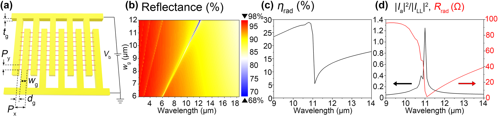
Grating-based nanoantenna fed by the Luttinger liquid array. (a) A device structure (w g : grating width, t g : grating thickness, d g : gap distance, l LL = d + 2l T : the feed length, l T : the overlap length, P x = w g + d g and P y : the period along the x and y-direction, respectively). Spectrum of (b) the reflectance according to the grating width w g upon the normally incident plane wave in the receiving operation. (c) The radiation efficiency η rad(λ 0), (d) the current strength ratio (|I a (λ 0)|2/|I LL (λ 0)|2), and the radiation resistance R rad(λ 0) for w g = 11 μm in the transmitting operation by the feed current source I 0.
3 Conclusions
We have proposed design principles to enhance the injection efficiency η inj and the radiation efficiency η rad of the Luttinger liquid-fed nanoantennas. Since the photon emission in our nanoantenna scheme is mediated by the two steps (i.e. electron injection and photon radiation), the resultant quantum efficiency η Q is given by η Q = η inj × η rad. In our previous work, we obtained η Q ∼3% without the optimization using the design principles we present in this work [17]. Here, we suggest that a much higher η Q is achievable via tailoring the electron injection scheme and the nanoantenna structure. Also, we propose that the grating nanoantennas can provide radiation efficiency η rad, even higher than rod nanoantennas. The grating nanoantennas can host multiple Luttinger liquid feeds within the metallic gap, making the photon emission intensity larger. This may be an advantage for proof-of-concept of the electrically driven Luttinger liquid-fed nanoantennas. Before concluding, we also emphasize that our scheme of the Luttinger liquid-fed nanoantennas works only on an electron-in/photon-out operation. However, its reverse process, i.e. a photon-in/electron-out operation, may be possible if we can extract electrons from optically excited Luttinger liquid plasmons. Research toward the bidirectional operation of the Luttinger liquid-fed nanoantenna can be an interesting direction to pursue.
Funding source: National Research Foundation of Korea
Award Identifier / Grant number: NRF-2022R1F1A1074019
-
Author contributions: All the authors wrote the manuscript. Jeon, Ko and Yoo conceived the project. Yoo calculated electron injection efficiency. Jeon and Ko performed numerical simulations for the radiation efficiency. Jeon and Ko contributed equally to this work.
-
Research funding: This work was supported by the National Research Foundation of Korea (NRF) grant funded by the Korea government (MSIT) (NRF-2022R1F1A1074019).
-
Conflict of interest statement: The authors declare no conflicts of interest regarding this article.
References
[1] M. Parzefall, P. Bharadwaj, A. Jain, T. Taniguchi, K. Watanabe, and L. Novotny, “Antenna-coupled photon emission from hexagonal boron nitride tunnel junctions,” Nat. Nanotechnol., vol. 10, p. 1058, 2015. https://doi.org/10.1038/nnano.2015.203.Search in Google Scholar PubMed
[2] P. Wang, A. V. Krasavin, M. E. Nasir, W. Dickson, and A. V. Zayats, “Reactive tunnel junctions in electrically driven plasmonic nanorod metamaterials,” Nat. Nanotechnol., vol. 13, p. 159, 2018. https://doi.org/10.1038/s41565-017-0017-7.Search in Google Scholar PubMed PubMed Central
[3] C. Zhang, J. P. Hugonin, A. L. Coutrot, C. Sauvan, F. Marquier, and J. J. Greffet, “Antenna surface plasmon emission by inelastic tunneling,” Nat. Commun., vol. 10, p. 4949, 2019. https://doi.org/10.1038/s41467-019-12866-3.Search in Google Scholar PubMed PubMed Central
[4] P. Chen, W. Wang, N. Lin, and S. Du, “Manipulating photon emission efficiency with local electronic states in a tunneling gap,” Opt. Express, vol. 22, p. 8234, 2014. https://doi.org/10.1364/oe.22.008234.Search in Google Scholar
[5] J. Kern, R. Kullock, J. Prangsma, M. Emmerling, M. Kamp, and B. Hecht, “Electrically driven optical antennas,” Nat. Photonics, vol. 9, p. 582, 2015. https://doi.org/10.1038/nphoton.2015.141.Search in Google Scholar
[6] J. C. Prangsma, J. Kern, A. G. Knapp, et al.., “Electrically connected resonant optical antennas,” Nano Lett., vol. 12, p. 3915, 2012. https://doi.org/10.1021/nl3007374.Search in Google Scholar PubMed
[7] P. Bharadwaj, A. Bouhelier, and L. Novotny, “Electrical excitation of surface plasmons,” Phys. Rev. Lett., vol. 106, p. 226802, 2011. https://doi.org/10.1103/physrevlett.106.226802.Search in Google Scholar PubMed
[8] M. Parzefall and L. Novotny, “Optical antennas driven by quantum tunneling: a key issues review,” Rep. Prog. Phys., vol. 82, p. 112401, 2019. https://doi.org/10.1088/1361-6633/ab4239.Search in Google Scholar PubMed
[9] K. Kaasbjerg and A. Nitzan, “Theory of light emission from quantum noise in plasmonic contacts: above-threshold emission from higher-order electron-plasmon scattering,” Phys. Rev. Lett., vol. 114, p. 126803, 2015. https://doi.org/10.1103/physrevlett.114.126803.Search in Google Scholar
[10] K. Braun, F. Laible, O. Hauler, et al.., “Active optical antennas driven by inelastic electron tunneling,” Nanophotonics, vol. 7, p. 1503, 2018. https://doi.org/10.1515/nanoph-2018-0080.Search in Google Scholar
[11] F. Bigourdan, J. P. Hugonin, F. Marquier, C. Sauvan, and J. J. Greffet, “Nanoantenna for electrical generation of surface plasmon polaritons,” Phys. Rev. Lett., vol. 116, p. 1, 2016. https://doi.org/10.1103/physrevlett.116.106803.Search in Google Scholar PubMed
[12] I. S. Maksymov, I. Staude, A. E. Miroshnichenko, and Y. S. Kivshar, “Optical yagi-uda nanoantennas,” Nanophotonics, vol. 1, p. 65, 2012. https://doi.org/10.1515/nanoph-2012-0005.Search in Google Scholar
[13] L. Ma, P. Yu, W. Wang, et al.., “Nanoantenna-enhanced light-emitting diodes: fundamental and recent progress,” Laser Photon. Rev., vol. 15, p. 2000367, 2021. https://doi.org/10.1002/lpor.202000367.Search in Google Scholar
[14] Y. Aytac, B. V. Olson, J. K. Kim, et al.., “Bandgap and temperature dependence of auger recombination in InAs/InAsSb type-II superlattices,” J. Appl. Phys., vol. 119, p. 215705, 2016. https://doi.org/10.1063/1.4953386.Search in Google Scholar
[15] H. P. Hjalmarson and S. R. Kurtz, “Electron auger processes in mid-infrared InAsSb/InGaAs heterostructures,” Appl. Phys. Lett., vol. 69, p. 949, 1996. https://doi.org/10.1063/1.117091.Search in Google Scholar
[16] B. Vinter, “Auger recombination in narrow-gap semiconductor superlattices,” Phys. Rev. B, vol. 66, p. 045324, 2002. https://doi.org/10.1103/physrevb.66.045324.Search in Google Scholar
[17] S. Yoo, S. Zhao, and F. Wang, “Infrared light-emitting devices from antenna-coupled luttinger liquid plasmons in carbon nanotubes,” Phys. Rev. Lett., vol. 127, p. 257702, 2021. https://doi.org/10.1103/physrevlett.127.257702.Search in Google Scholar PubMed
[18] M. Bockrath, D. H. Cobden, P. L. McEuen, et al.., “Single-electron transport in ropes of carbon nanotubes,” Science, vol. 275, p. 1922, 1997. https://doi.org/10.1126/science.275.5308.1922.Search in Google Scholar PubMed
[19] M. Bockrath, D. H. Cobden, J. Lu, et al.., “Luttinger-liquid behaviour in carbon nanotubes,” Nature, vol. 397, p. 598, 1999. https://doi.org/10.1038/17569.Search in Google Scholar
[20] S. Zhao, S. Wang, F. Wu, et al.., “Correlation of electron tunneling and plasmon propagation in a Luttinger liquid,” Phys. Rev. Lett., vol. 121, p. 047702, 2018. https://doi.org/10.1103/physrevlett.121.047702.Search in Google Scholar
[21] Z. Shi, X. Hong, H. A. Bechtel, et al.., “Observation of a Luttinger-liquid plasmon in metallic single-walled carbon nanotubes,” Nat. Photonics, vol. 9, p. 515, 2015. https://doi.org/10.1038/nphoton.2015.123.Search in Google Scholar
[22] S. Wang, F. Wu, S. Zhao, et al.., “Logarithm diameter scaling and carrier density independence of one-dimensional Luttinger liquid plasmon,” Nano Lett., vol. 19, p. 2360, 2019. https://doi.org/10.1021/acs.nanolett.8b05031.Search in Google Scholar PubMed
[23] J. Voit, “A brief introduction to Luttinger liquids,” AIP Conf. Proc., vol. 544, pp. 309–318, 2000.10.1063/1.1342524Search in Google Scholar
[24] M. Ouyang, J. L. Huang, and C. M. Lieber, “One-dimensional energy dispersion of single-walled carbon nanotubes by resonant electron scattering,” Phys. Rev. Lett., vol. 88, p. 4, 2002. https://doi.org/10.1103/physrevlett.88.066804.Search in Google Scholar
[25] K. Liu, J. Deslippe, F. Xiao, et al.., “An atlas of carbon nanotube optical transitions,” Nat. Nanotechnol., vol. 7, p. 325, 2012. https://doi.org/10.1038/nnano.2012.52.Search in Google Scholar PubMed
[26] J. Wang, J. Niu, B. Shao, et al.., “A tied Fermi liquid to Luttinger liquid model for nonlinear transport in conducting polymers,” Nat. Commun., vol. 12, p. 1, 2021. https://doi.org/10.1038/s41467-020-20238-5.Search in Google Scholar PubMed PubMed Central
[27] W. Jolie, C. Murray, P. S. Weiß, et al.., “Tomonaga-Luttinger liquid in a box: electrons confined within MoS2 mirror-twin boundaries,” Phys. Rev. X, vol. 9, p. 11055, 2019. https://doi.org/10.1103/physrevx.9.011055.Search in Google Scholar
[28] P. Wang, G. Yu, Y. H. Kwan, et al.., “One-dimensional Luttinger liquids in a two-dimensional moiré lattice,” Nature, vol. 605, p. 57, 2022. https://doi.org/10.1038/s41586-022-04514-6.Search in Google Scholar PubMed
[29] J. Voit, “One-dimensional Fermi liquids,” Rep. Prog. Phys., vol. 58, p. 977, 1995. https://doi.org/10.1088/0034-4885/58/9/002.Search in Google Scholar
[30] C. Kane, L. Balents, and M. Fisher, “Coulomb interactions and mesoscopic effects in carbon nanotubes,” Phys. Rev. Lett., vol. 79, p. 5086, 1997. https://doi.org/10.1103/physrevlett.79.5086.Search in Google Scholar
[31] X. Luo, C. Hu, B. Lyu, et al.., “Reflection phase shift of one-dimensional plasmon polaritons in carbon nanotubes,” Phys. Rev. B, vol. 101, p. 041407, 2020. https://doi.org/10.1103/physrevb.101.041407.Search in Google Scholar
[32] F. C. Simeone, H. J. Yoon, M. M. Thuo, J. R. Barber, B. Smith, and G. M. Whitesides, “Defining the value of injection current and effective electrical contact area for EGaIn-based molecular tunneling junctions,” J. Am. Chem. Soc., vol. 135, p. 18131, 2013. https://doi.org/10.1021/ja408652h.Search in Google Scholar PubMed
[33] J.-Y. Park, S. Rosenblatt, Y. Yaish, et al.., “Electron−Phonon scattering in metallic single-walled carbon nanotubes,” Nano Lett., vol. 4, p. 517, 2004. https://doi.org/10.1021/nl035258c.Search in Google Scholar
[34] A. T. de Hoop and G. de Jong, “Power reciprocity in antenna theory,” Proc. Inst. Electr. Eng., vol. 121, p. 1051, 1974. https://doi.org/10.1049/piee.1974.0247.Search in Google Scholar
[35] R. L. Olmon, B. Slovick, T. W. Johnson, et al.., “Optical dielectric function of gold,” Phys. Rev. B, vol. 86, p. 235147, 2012. https://doi.org/10.1103/physrevb.86.235147.Search in Google Scholar
[36] S. Wang, S. Yoo, S. Zhao, et al.., “Gate-tunable plasmons in mixed-dimensional van Der Waals heterostructures,” Nat. Commun., vol. 12, p. 5039, 2021. https://doi.org/10.1038/s41467-021-25269-0.Search in Google Scholar PubMed PubMed Central
[37] M. S. Eggleston, K. Messer, L. Zhang, E. Yablonovitch, and M. C. Wu, “Optical antenna enhanced spontaneous emission,” Proc. Natl. Acad. Sci., vol. 112, p. 1704, 2015. https://doi.org/10.1073/pnas.1423294112.Search in Google Scholar PubMed PubMed Central
[38] M. Staffaroni, J. Conway, S. Vedantam, J. Tang, and E. Yablonovitch, “Circuit analysis in metal-optics,” Photonics Nanostructures – Fundam. Appl., vol. 10, p. 166, 2012. https://doi.org/10.1016/j.photonics.2011.12.002.Search in Google Scholar
[39] A. Kumar, T. Low, K. H. Fung, P. Avouris, and N. X. Fang, “Tunable light–matter interaction and the role of hyperbolicity in graphene–HBN system,” Nano Lett., vol. 15, p. 3172, 2015. https://doi.org/10.1021/acs.nanolett.5b01191.Search in Google Scholar PubMed
[40] A. Woessner, M. B. Lundeberg, Y. Gao, et al.., “Highly confined low-loss plasmons in graphene–boron nitride heterostructures,” Nat. Mater., vol. 14, p. 421, 2015. https://doi.org/10.1038/nmat4169.Search in Google Scholar PubMed
[41] A. J. Yang, K. Han, K. Huang, et al.., “Van der Waals integration of high-κ perovskite oxides and two-dimensional semiconductors,” Nat. Electron., vol. 5, p. 233, 2022. https://doi.org/10.1038/s41928-022-00753-7.Search in Google Scholar
[42] J. Wang, H. Lai, X. Huang, et al.., “High-κ van Der Waals oxide MoO3 as efficient gate dielectric for MoS2 field-effect transistors,” Materials, vol. 15, p. 5859, 2022. https://doi.org/10.3390/ma15175859.Search in Google Scholar PubMed PubMed Central
[43] S. Foteinopoulou, G. C. R. Devarapu, G. S. Subramania, S. Krishna, and D. Wasserman, “Phonon-polaritonics: enabling powerful capabilities for infrared photonics,” Nanophotonics, vol. 8, p. 2129, 2019. https://doi.org/10.1515/nanoph-2019-0232.Search in Google Scholar
[44] M. Killi, T. C. Wei, I. Affleck, and A. Paramekanti, “Tunable Luttinger liquid physics in biased bilayer graphene,” Phys. Rev. Lett., vol. 104, p. 1, 2010. https://doi.org/10.1103/physrevlett.104.216406.Search in Google Scholar PubMed
[45] C. Chen, A. H. C. Neto, and V. M. Pereira, “Correlated states of a triangular net of coupled quantum wires: implications for the phase diagram of marginally twisted bilayer graphene,” Phys. Rev. B, vol. 101, p. 165431, 2020. https://doi.org/10.1103/physrevb.101.165431.Search in Google Scholar
Supplementary Material
This article contains supplementary material (https://doi.org/10.1515/nanoph-2022-0782).
© 2023 the author(s), published by De Gruyter, Berlin/Boston
This work is licensed under the Creative Commons Attribution 4.0 International License.
Articles in the same Issue
- Frontmatter
- Editorial
- Special issue: Metamaterials and plasmonics in Asia, a tribute to Byoungho Lee
- Memorandum
- In memory of Prof. Byoungho Lee
- Reviews
- Advances and applications on non-Hermitian topological photonics
- Topological phases and non-Hermitian topology in photonic artificial microstructures
- Recent advanced applications of metasurfaces in multi-dimensions
- Recent advances in oblique plane microscopy
- Research Articles
- A symmetry-protected exceptional ring in a photonic crystal with negative index media
- Highly angle-sensitive and efficient optical metasurfaces with broken mirror symmetry
- Multilayer all-polymer metasurface stacked on optical fiber via sequential micro-punching process
- Inverse design of high-NA metalens for maskless lithography
- Deterministic approach to design passive anomalous-diffraction metasurfaces with nearly 100% efficiency
- Metasurface spatial filters for multiple harmonic signals
- Multiple symmetry protected BIC lines in two dimensional synthetic parameter space
- Deep-learning-assisted reconfigurable metasurface antenna for real-time holographic beam steering
- On-chip integration of metasurface-doublet for optical phased array with enhanced beam steering
- Multi-frequency amplitude-programmable metasurface for multi-channel electromagnetic controls
- Broadband absorber with dispersive metamaterials
- Visible-mid infrared ultra-broadband and wide-angle metamaterial perfect absorber based on cermet films with nano-cone structure
- Vertical photon sorting by stacking silicon and germanium nanopillars for broadband absorbers
- Directive emission from polymeric fluorophore with epsilon-near-zero squaraine molecular film
- Chiral-magic angle of nanoimprint meta-device
- Fluorescence engineering in metamaterial-assisted super-resolution localization microscope
- Nano-shaping of chiral photons
- Design principles for electrically driven Luttinger liquid-fed plasmonic nanoantennas
- Ultrafast strong-field terahertz nonlinear nanometasurfaces
- Reconfigurable anomalous reflectors with stretchable elastic substrates at 140 GHz band
- Polarization-independent isotropic metasurface with high refractive index, low reflectance, and high transmittance in the 0.3-THz band
- Terahertz nanofuse by a single nanowire-combined nanoantenna
- Electrically tunable THz graphene metasurface wave retarders
- Ultra-thin grating coupler for guided exciton-polaritons in WS2 multilayers
- Reflection of two-dimensional surface polaritons by metallic nano-plates on atomically thin crystals
- A deep neural network for general scattering matrix
- Engineering isospectrality in multidimensional photonic systems
- Heterogeneously integrated light emitting diodes and photodetectors in the metal-insulator-metal waveguide platform
- DNA origami-designed 3D phononic crystals
- All-dielectric carpet cloaks with three-dimensional anisotropy control