
Plasmons compressing the light – a jewel in the treasure chest of Mark Stockman’s legacy
-
Jacob B. Khurgin


Abstract
Among all the contributions made by Mark Stockman, his work on concentrating the light energy to unprecedented densities is one of the most remarkable achievements. Here it is briefly reviewed and a relatively novel, intuitive, and physically transparent interpretation of nanofocusing using the effective volume of hybrid coupled modes formalism is presented and the role of Landau damping as the main limiting factor is highlighted.
1 Introduction
Professor Mark I. Stockman of Georgia State University, a towering figure in photonics and a force behind numerous trailblazing advances in nanophotonics, and more specifically plasmonics, passed away in November 2020. It will take time for the world of science to recognize what a significant and irreparable loss it has been and to properly assess the breadth and depths of Mark’s contributions made over the course of five decades. Still, it is not too early to recognize Mark’s key contributions that have the deepest impact on the course of progress in photonics.
Mark’s work on coherent sources of surface plasmons (SPASER) [1, 2] is probably the most widely recognized one, but it would be a great disservice to his legacy to omit other, in my view, no less important contributions to nanophotonics. Among them, his innovative ideas in the field of nanoscopy and nanofocusing do stand out and thus deserve a special attention. The whole idea of nanofocusing (i.e. concentrating the light into subwavelength volumes) using photonic and plasmonic nanoscale structures has been discussed for many years [3], but it took Mark Stockman to bring it closer to reality when he first introduced concepts of adiabatic focusing [4] and focusing using selfsimilar chains of nanoparticles [5]. These ideas have been further developed by the community and have established the means of both effective focusing of light into miniscule volumes [6] and, most remarkably, accelerating by orders of magnitudes the spontaneous emission rates via the Purcell effect [7, 8]. These achievements are already finding applications in nanoscale sensing and in the development of efficient single photon sources.
In 2003 Mark Stockman, working with colleagues Kuiru Li and David Bergman, was the first one to come up with this groundbreaking idea that using a chain of selfsimilar (i.e. having the same shape) nanoparticles with progressively decreasing sizes can focus the light into the gap between the smallest nanospheres where the local fields are enhanced by orders of magnitude [5]. In this work Mark and his colleagues skillfully utilized the fact that the resonant frequencies of subwavelength localized surface plasmons (LSPs) depend only on the shape and not on the size of the modes, and that allows efficient resonant transfer of power along the chain in both directions; i.e. it can enhance both absorption and emission of light.
Shortly thereafter, in 2004 Mark expanded the concept of adiabatic light concentration to propagating surface plasmon polaritons (SPPs) in the tapered plasmonic waveguide, and it is this type of light concentration that has become known as “nanofocusing” in a narrow sense. As the width of the waveguide and the effective wavelength of SPP are reduced, the impedance gradually increases and reaches values almost comparable to those of atomic and molecular dipoles. The key to efficient transfer of energy is the fact that the width (and hence impedance) are changing adiabatically; hence the reflection is almost nonexistent and the only limitation to efficiency is metal absorption. In his work Mark has taken previous work on polariton nanofocusing [9] farther along to practical implementations achieved since his pioneering contribution [6].
Concurrently with the aforementioned work on light concentration, Mark Stockman (in collaboration with Peter Nordlander’s group at Rice University) has pointed that significant enhancement can be attained in plasmonic dimers. As discussed in [10] the dimer acts as an optical antenna with low impedance while its gap mode acts as a high impedance cavity [11] and was exploited in achieving record high emission rates for quantum emitters [8].
And yet, despite the large number of experimental results, computer models, and theoretical analyses, the question of what kind of ultimate enhancement can be attained using the principle of adiabatic nanofocusing remains open. Furthermore, various groups approach it from different angles. Some, approaches that can be traced to electromagnetic (EM) theory emphasize the impedance matching between antenna and atom or molecule (to which we shall refer as a quantum oscillator) [12], [13], [14], while others concentrate on local density of states [15], and yet other approaches treat the complex plasmonic structures as coupled oscillators [11, 16]. The nanophotonics community could benefit from a unified theory of adiabatic nanofocusing (and the reverse process of emission enhancement) which would show the equivalence of different approaches using a very simple and transparent model in a way Mark Stockman always presented his work, i.e. with clarity, depth, and succinctness. These days computing power at our disposal allows us to resolve many physical problems with speed and efficiency which would have been seen beyond the realm of possible only a few decades ago. But with the growing preponderance of numerical method something is in danger of being lost. That something is the ability to present a simple a clear picture of the physics behind complicated phenomena, and it is this ability that made Mark Stockman stand out among his peers. Alas, Mark is no longer available to undertake this task, so, this paper is an attempt to explain light concertation on nanoscale to a wide audience to the best of my rather modest abilities, with a hope that this work will serve as a tribute to Mark’s rich legacy.
This work has been conceived as neither a review nor a comprehensive tutorial. It combines previously known concepts with a number of new insights which may help the reader to get an intuitive feel for nanofocusing and appreciate Mark Stockman’s foresight. Plasmonics is a truly multidisciplinary science and the same problem of light concentrating can be approached from the point of view of electrical engineer (impedance matching), quantum optics (density of states), or physical optics (absorption and emission cross-sections). Here I attempt to show how all these approaches lead to the same results, which, in my view has certain pedagogical value. First I briefly review the idea of nanofocusing as impedance matching between free space and the quantum oscillator. Then a coupled oscillator model will be described to explain the energy concentration in plasmonic dimers and trimers. A novel concept of coupled mode having two different “effective volumes” – one as a cavity and one as an antenna – will be developed and related to the local density of states. A coupled mode model will be then further extended to the “hybrid modes” incorporating quantum oscillators and metallic nanoparticles. It will be shown that ultimately the degree of enhancement is limited by the minimum size of the smallest nanoparticle (∼10 nm) at which the onset of Landau damping broadens the linewidth of resonance and thus limits the enhancement. The last section contains the conclusions that further emphasize foresight of Mark Stockman and his contribution to nanophotonics.
2 Quantum oscillator and its impedance
The quantum oscillator, which can be an atom, a molecule, and exciton, or a quantum dot, and can be both an absorber and emitter, was first treated as a two-level system by Greffet et al. in [14]. The impedance was introduced using Green’s function and related to local density of states. Here the somewhat different approach leading to the same circuit model is considered. In the presence of external field Eext with frequency ω the two level system with resonant frequency ω
21 and transition matrix element
where γ
a
is the dephasing rate. The physical size (effective radius) of the oscillator can be approximated as
where
with three terms inside the brackets corresponding to the resistance, inductance, and capacitance, all connected in series (Figure 1a), as first noted in [14].
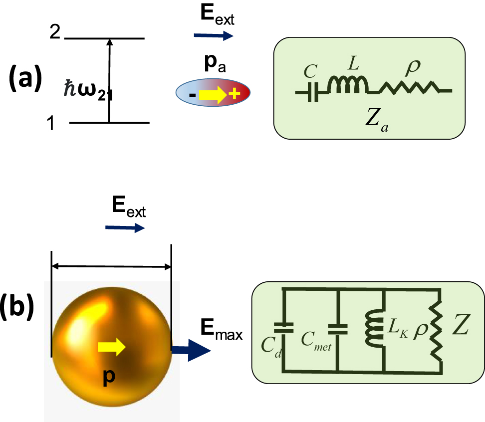
(a) Two-quantum oscillator and its circuit model, (b) localized surface plasmon (LSP) mode on a metal nanoparticle and its circuit model.
On resonance one obtains
where
 η
0, however when one considers transfer of energy in space, it is the impedance per unit area that matters [14, 17], i.e. dividing (2) by
η
0, however when one considers transfer of energy in space, it is the impedance per unit area that matters [14, 17], i.e. dividing (2) by
The impedance mismatch between the quantum oscillator and free space is therefore
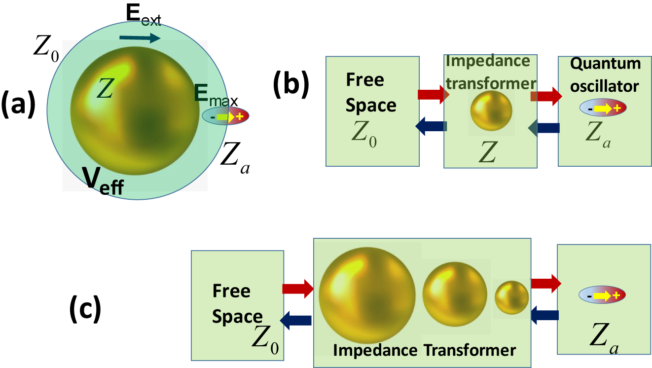
or anywhere between 6 and 8 orders of magnitude, even for the allowed transition, and more than that for weaker, forbidden transition. (Note that this mismatch is essentially a ratio between the diameter of diffraction limited focused beam and resonant absorption cross-section of the atom or molecule indicating the connection between the electrical engineering and physical optics approaches). Clearly, to match impedances one has to resort to using an antenna that serves as impedance transformer. Such a transformer can be a nanoparticle supporting the LSP. Intuitively the dimensions of that mode should be on the order of the geometric mean between wavelength and atomic dipole, i.e. few tens of nanometers.
3 Nanofocusing as impedance matching
Let us now determine the impedance of an LSP of the plasmonic nanoparticle shown in Figure 1b. A spherical nanoparticle with a diameter d is shown in Figure 1b, but the theory developed here can be easily applied to the other shapes. Following the theory of Engheta and Alu [12], we consider a nanoparticle made from a metal with dielectric constant
The first term corresponds to the capacitance, C
mat
the second to the kinetic inductance, L
K
and the last one to the resistance ρ, all connected in parallel as displayed in Figure 1b. In addition, there is also a capacitance associated with the field in the dielectric C
d
. The capacitance scales with diameter d while inductance and resistance are inversely proportional to it. Overall, assuming
where coefficients B c and B L are shape-dependent coefficients, both on the order of unity and coefficient β corresponds to the fraction of electric field in the dielectric. Clearly the resonance occurs when
For the spherical particle one can show that B C =B L and β=2 so that a familiar expression for the LSP resonance emerges
On resonance
As one can see, the impedance decreases dramatically with the size of the nanoparticle. It should also be noted that the resonant frequency does not depend on the actual size of the nanoparticle because in (9) we neglect the “normal” inductance due to magnetic field induced by the current in the metal,
leading to the resonance condition
Now, when one considers impedance mismatch one has to realize that the energy transfer takes place only across a fraction of the surface; hence it makes sense to define the impedance per unit area as shown in [14]
i.e. proportional to the effective local density of states
for a wide range of Q’s. These numbers are not far from the ones found optimal in [19, 21], but it has also been shown this does not lead to the absorption (emission) enhancement exceeding
(a) LSP mode enhancing field near the quantum oscillator, (b) circuit model of absorption/emission enhancement as impedance matching and (c) impedance matching with a chain of nanoparticles.
The rest of this paper is devoted to exploring focusing with plasmonic dimers [28] and trimers [29]. While using impedances conveniently relates the issue to the classical impedance matching in electrical engineering, it is also worthwhile to explore the same issue from a different point of view – by developing an analytical coupled mode model for the chain of nanoparticles [30], [31], [32]. Previously, this model has only been used for plasmonic dimers and the role of damping was not explored, but in this work it is extended to three and more nanoparticles. Doing so allows one to see clearly how the adiabaticity allows one to increase degree of field enhancement, and to concurrently explore the limits of this enhancement
4 Coupled modes theory – plasmonic dimer
First, one shall note that the dipole moment of the LSP on a nanosphere of Figure 2a is
where
where the LSP resonant frequency ω 0 is given in (11) and the DC polarizability is
(for the case when
Now, it is possible to relate the dipole and the total energy of the LSP mode as
where a new variable a is a square root of energy in LSP mode (classical analogue of plasmon annihilation operator). Now
and (19) becomes
where
It is also possible to relate a to the magnitude of the electric field on the surface of the nanoparticle,
and introduce the effective volume
so that
Finally, one obtains
Where the “material” factor is
For
where the maximum enhancement by a single nanoparticle F
1=AQ. Thus with a single nanoparticle maximum field enhancement is just on the order of Q factor, i.e. no more than 10–20 times. Note that the ratio between the effective volume and nanoparticle volume (25) can be written as
Let us now consider coupling between two nanoparticles separated by distance r 12, as shown in Figure 3a. The field of the larger nanoparticle at the center of the smaller nanoparticle is
and the coupling coefficient is obtained by substituting (30) into (22)
where
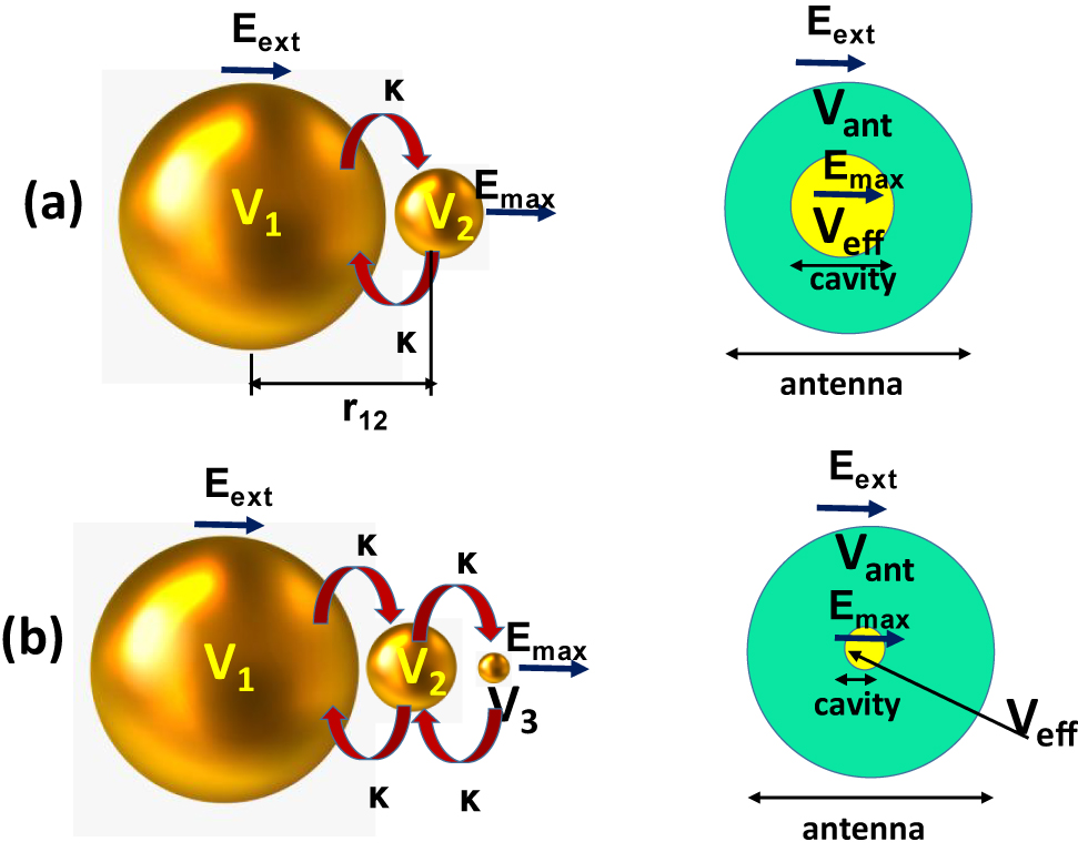
Energy transfer in (a) plasmonic dimer and (b) plasmonic trimer. On the right hand side the couple modes are represented as oscillators with large volume as an antenna
Now if one introduces symmetric and antisymmetric super-modes
adding and subtracting two lines in (32) yields
The “effective polarizabilities” for two super-modes are
where the “effective volume as an antenna” has been introduced as
Clearly, for vastly dissimilar nanoparticles
Now, effective volume as a cavity for each mode can be found from the fact that the energy is equally divided between two nanoparticles, and since the maximum field is at the surface of a smaller nanoparticle,
The dimer mode behaves as a large antenna, and at the same time it behaves as a small cavity, which is exactly what is needed for strong field enhancement as shown schematically on the right hand side of Figure 3a.
When the light with a resonance frequency
and the maximum field in the symmetric mode is
The enhancement occurs because for the supermode the antenna volume is determined primarily by the larger nanoparticls, while the effective cavity volume by the small nanoparticle. The additional enhancement factor is
From this expression it follows that F s can become arbitrary large as K increases. However, there is also the asymmetric mode, and in that mode the dipole of small nanoparticle is directed against the one excited in the symmetric mode, i.e.
Substituting (31) we obtain for the added enhancement in dimer,
In Figure 4a the total dimer enhancement
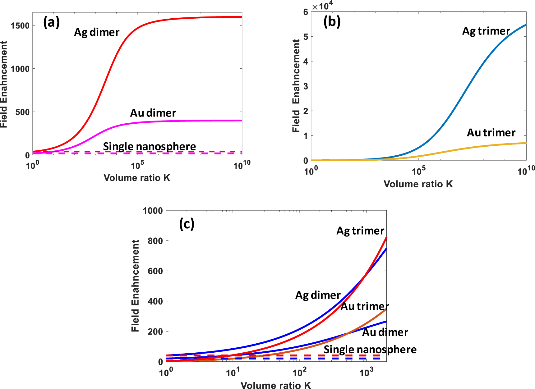
Field enhancement in (a) plasmonic dimers, (b) plasmonic trimers, and (c) zoomed in practical region where enhancement is not impeded by Landau damping.
The total enhancement in dimer is therefore
5 Extension of coupled mode theory to three and more nanoparticles
The task of reducing the volume of smallest nanoparticle while keeping coupling strong can be accomplished by inserting an intermediary nanoparticle between the “antenna” V
1 and “cavity”
where according to (31)
For large K coupling
with resonance frequencies ω
0,
The effective volumes as antennas for three modes, shown in Figure 3b are
Once again, the effective volume as an antenna (i.e. effective dipole) is determined by the largest nanoparticle hence the trimer can effectively couple to the free space. Operating at resonance frequency we immediately obtain
The effective volumes as cavities are
These volumes, determined by the smallest nanoparticle are small which is advantageous for coupling to the angstrom-size quantum oscillators. The maximum fields on resonance are
Thus additional field enhancement with trimer antenna is therefore
In Figure 4b the total dimer enhancement
and the total trimer field enhancement is
6 Effective volume for quantum absorber/emitter and its use for quantifying absorption and emission enhancement
As has been mentioned above, it had been shown that quantum entity, emitter, or absorber can be represented by a circuit model with L, C, and R is series and characterized by impedance Z(ω). Here and alternative is presented. This alternative consists of representing quantum emitter/absorber as a classical dipole oscillator, characterized (in addition to resonance frequency ω 12 and damping rate γ a ) by the effective volume V eff,a . This model can then be applied to describe absorption and emission by quantum oscillator as well as its coupling to the antennas. The energy of a quantum oscillator and its dipole are related as
Therefore, we can introduce the “amplitude” of the atomic motion as a square root of its energy, or, essentially, a classical analogue of annihilation operator.
Substituting it into Eq. (1) one obtains
and the differential equation for a a is
where
If we now compare (59) with (27) we can even introduce the effective volume for the quantum oscillator
Since in the visible/near IR region the dipole for an allowed transition
Now, the coupling of energy into a quantum absorber using a nanoantenna consisting of N nanospheres can be approached as coupling into a hybrid supermode with N+1 entities – N nanospheres and a quantum oscillator. Such a hybrid mode has effective dipole that exceeds r
12 by many orders of magnitude. In Figure 5a a dimer antenna with nanospheres of volumes V
1 and V
2 coupled into the quantum absorber with effective volume V
eff,a
is represented as a hybrid trimer. If the absorber is resonant with the antenna, ω
12=ω
0, one can see that the optimum coupling will be achieved when
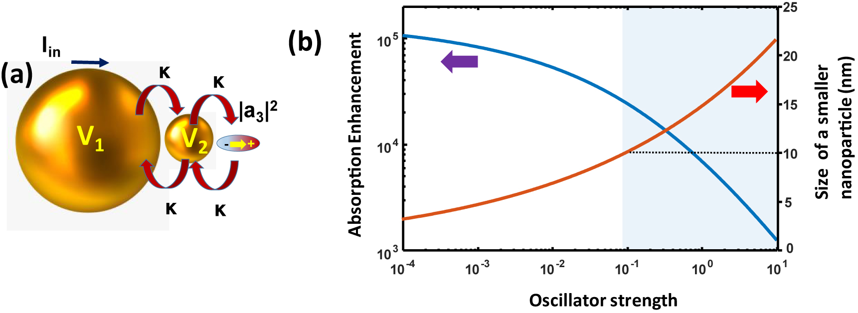
(a) Nanofocusing in a hybrid trimer consisting of a plasmonic dimer and quantum oscillator. (b) Enhancement of absorption. Shaded region represents a practical range of enhancement not impeded by excessive Landau damping.
In the absence of nanoantenna the absorption cross section is
Therefore, the absorption cross-section with dipole antenna gets enhanced
Note that here the decay rates of atomic oscillator and LSP has been assumed to be equal. If they are not equal, one has to introduce the weighted average γ which will change the results but not all that significantly unless
7 Conclusions
In this work Mark Stockman’s contributions to just one area of photonics has been highlighted. Thanks to him, the idea of nanofocusing took root in the community, and plenty of theoretical and experimental works have followed. Perhaps inevitably, the original idea often became compromised by excessive hype and unsustainable claims, but the core of Mark predictions has been indeed confirmed. Plasmonics undeniably offers unique chance to confine light into minuscule volumes and achieve very strong fields which can be used for probing the matter on a nanoscale [36], if not for more exotic applications in photonic integrated circuits and light sources. Excessive loss due to Landau damping does prevent us from fully realizing the nanofocusing potential, but it Is not entirely impossible that the issue of loss will be addressed in the future. Before I conclude, I should note that Mark Stockman himself never oversold his ideas and habitually offered a sober and critical assessment of trendy topics, be that negative refraction [37, 38], epsilon near zero materials [39], spoof plasmons [40] and other. His critical eye and sober mind will be just as missed as his unabashed enthusiasm for science, never ending quest for discovery, and his zest for life which he preserved all the way to the end.
Acknowledgement
As always, in this work I was aided, supported and comforted by my steadfast colleagues Prof. P. Noir and Dr. S. Artois – without their devotion this work would have never come to fruition.
-
Author contribution: The author have accepted responsibility for the entire content of this submitted manuscript and approved submission.
-
Research funding: None declared.
-
Conflict of interest statement: The author declares no conflicts of interest regarding this article.
References
[1] M. I. Stockman, “Spasers explained,” Nat. Photonics, vol. 2, pp. 327–329, 2008. https://doi.org/10.1038/nphoton.2008.85.Suche in Google Scholar
[2] D. J. Bergman and M. I. Stockman, “Surface plasmon amplification by stimulated emission of radiation: quantum generation of coherent surface plasmons in nanosystems,” Phys. Rev. Lett., vol. 90, 2003, Art no. 027402. https://doi.org/10.1103/physrevlett.90.027402.Suche in Google Scholar PubMed
[3] J. R. Krenn, A. Dereux, J. C. Weeber, et al.., “Squeezing the optical near-field zone by plasmon coupling of metallic nanoparticles,” Phys. Rev. Lett., vol. 82, pp. 2590–2593, 1999. https://doi.org/10.1103/physrevlett.82.2590.Suche in Google Scholar
[4] M. I. Stockman, “Nanofocusing of optical energy in tapered plasmonic waveguides,” Phys. Rev. Lett., vol. 93, 2004, Art no. 137404. https://doi.org/10.1103/physrevlett.93.137404.Suche in Google Scholar PubMed
[5] K. Li, M. I. Stockman, and D. J. Bergman, “Self-similar chain of metal nanospheres as an efficient nanolens,” Phys. Rev. Lett., vol. 91, 2003, Art no. 227402. https://doi.org/10.1103/physrevlett.91.227402.Suche in Google Scholar
[6] D. K. Gramotnev and S. I. Bozhevolnyi, “Nanofocusing of electromagnetic radiation,” Nat. Photonics, vol. 8, pp. 13–22, 2014. https://doi.org/10.1038/nphoton.2013.232.Suche in Google Scholar
[7] T. B. Hoang, G. M. Akselrod, and M. H. Mikkelsen, “Ultrafast room-temperature single photon emission from quantum dots coupled to plasmonic nanocavities,” Nano Lett., vol. 16, pp. 270–275, 2016. https://doi.org/10.1021/acs.nanolett.5b03724.Suche in Google Scholar PubMed
[8] S. I. Bogdanov, O. A. Makarova, X. Xu, et al.., “Ultrafast quantum photonics enabled by coupling plasmonic nanocavities to strongly radiative antennas,” Optica, vol. 7, pp. 463–469, 2020. https://doi.org/10.1364/optica.382841.Suche in Google Scholar
[9] K. V. Nerkararyan, “Superfocusing of a surface polariton in a wedge-like structure,” Phys. Lett., vol. 237, pp. 103–105, 1997. https://doi.org/10.1016/s0375-9601(97)00722-6.Suche in Google Scholar
[10] P. Nordlander and E. Prodan, “Plasmon hybridization in nanoparticles near metallic surfaces,” Nano Lett., vol. 4, pp. 2209–2213, 2004. https://doi.org/10.1021/nl0486160.Suche in Google Scholar
[11] G. Sun, J. B. Khurgin, and A. Bratkovsky, “Coupled-mode theory of field enhancement in complex metal nanostructures,” Phys. Rev. B, vol. 84, 2011, Art no. 045415. https://doi.org/10.1103/physrevb.84.045415.Suche in Google Scholar
[12] A. Alù and N. Engheta, “Input impedance, nanocircuit loading, and radiation tuning of optical nanoantennas,” Phys. Rev. Lett., vol. 101, 2008, Art no. 043901. https://doi.org/10.1103/PhysRevLett.101.043901.Suche in Google Scholar PubMed
[13] N. Engheta, A. Salandrino, and A. Alù, “Circuit elements at optical frequencies: nanoinductors, nanocapacitors, and nanoresistors,” Phys. Rev. Lett., vol. 95, 2005, Art no. 095504. https://doi.org/10.1103/physrevlett.95.095504.Suche in Google Scholar
[14] J.-J. Greffet, M. Laroche, and F. Marquier, “Impedance of a nanoantenna and a single quantum emitter,” Phys. Rev. Lett., vol. 105, 2010, Art no. 117701. https://doi.org/10.1103/physrevlett.105.117701.Suche in Google Scholar PubMed
[15] P. Bharadwaj, B. Deutsch, and L. Novotny, “Optical antennas,” Adv. Opt Photon, vol. 1, pp. 438–483, 2009. https://doi.org/10.1364/aop.1.000438.Suche in Google Scholar
[16] G. Sun and J. B. Khurgin, “Comparative study of field enhancement between isolated and coupled metal nanoparticles: an analytical approach,” Appl. Phys. Lett., vol. 97, 2010, Art no. 263110. https://doi.org/10.1063/1.3532101.Suche in Google Scholar
[17] R. L. Olmon and M. B. Raschke, “Antenna-load interactions at optical frequencies: impedance matching to quantum systems,” Nanotechnology, vol. 23, 2012, Art no. 444001. https://doi.org/10.1088/0957-4484/23/44/444001.Suche in Google Scholar PubMed
[18] L. Novotny, “Effective wavelength scaling for optical antennas,” Phys. Rev. Lett., vol. 98, 2007, Art no. 266802. https://doi.org/10.1103/physrevlett.98.266802.Suche in Google Scholar PubMed
[19] J. B. Khurgin, G. Sun, and R. A. Soref, “Practical limits of absorption enhancement near metal nanoparticles,” Appl. Phys. Lett., vol. 94, 2009, Art no. 071103. https://doi.org/10.1063/1.3081631.Suche in Google Scholar
[20] A. F. Koenderink, “On the use of Purcell factors for plasmon antennas,” Opt. Lett., vol. 35, pp. 4208–4210, 2010. https://doi.org/10.1364/ol.35.004208.Suche in Google Scholar
[21] S. I. Bozhevolnyi and J. B. Khurgin, “Fundamental limitations in spontaneous emission rate of single-photon sources,” Optica, vol. 3, pp. 1418–1421, 2016. https://doi.org/10.1364/optica.3.001418.Suche in Google Scholar
[22] D. D. Ryutov, “Landau damping: half a century with the great discovery,” Plasma Phys. Contr. Fusion, vol. 41, p. A1, 1999. https://doi.org/10.1088/0741-3335/41/3a/001.Suche in Google Scholar
[23] J. Khurgin, W. Y. Tsai, D. P. Tsai, and G. Sun, “Landau damping and limit to field confinement and enhancement in plasmonic dimers,” ACS Photonics, vol. 4, pp. 2871–2880, 2017. https://doi.org/10.1021/acsphotonics.7b00860.Suche in Google Scholar
[24] T. V. Shahbazyan, “Landau damping of surface plasmons in metal nanostructures,” Phys. Rev. B, vol. 94, no. 1–9, p. 235431, 2016. https://doi.org/10.1103/physrevb.94.235431.Suche in Google Scholar
[25] J. B. Khurgin, “Ultimate limit of field confinement by surface plasmon polaritons,” Faraday Discuss., vol. 178, pp. 109–122, 2015. https://doi.org/10.1039/c4fd00193a.Suche in Google Scholar PubMed
[26] U. Kreibig and L. Genzel, “Optical-absorption of small metallic particles,” Surf. Sci., vol. 156, pp. 678–700, 1985. https://doi.org/10.1016/0039-6028(85)90239-0.Suche in Google Scholar
[27] U. Kreibig and M. Vollmer, Optical Properties of Metal Clusters, Springer Series in Materials Science, Berlin, New York, Springer, 1995, p. 532.10.1007/978-3-662-09109-8Suche in Google Scholar
[28] P. Nordlander, C. Oubre, E. Prodan, K. Li, and M. I. Stockman, “Plasmon hybridization in nanoparticle dimers,” Nano Lett., vol. 4, pp. 899–903, 2004. https://doi.org/10.1021/nl049681c.Suche in Google Scholar
[29] D. W. Brandl, N. A. Mirin, and P. Nordlander, “Plasmon modes of nanosphere trimers and quadrumers,” J. Phys. Chem. B, vol. 110, pp. 12302–12310, 2006. https://doi.org/10.1021/jp0613485.Suche in Google Scholar PubMed
[30] G. Sun and J. B. Khurgin, “Theory of optical emission enhancement by coupled metal nanoparticles: an analytical approach,” Appl. Phys. Lett., vol. 98, p. 113116, 2011. https://doi.org/10.1063/1.3565170.Suche in Google Scholar
[31] G. Sun and J. B. Khurgin, “Optimization of the nanolens consisting of coupled metal nanoparticles: an analytical approach,” Appl. Phys. Lett., vol. 98, p. 153115, 2011. https://doi.org/10.1063/1.3581886.Suche in Google Scholar
[32] G. Sun, J. B. Khurgin, and A. Bratkovsky, “Coupled-mode theory of field enhancement in complex metal nanostructures,” Phys. Rev. B, vol. 84, p. 045415, 2011.10.1103/PhysRevB.84.045415Suche in Google Scholar
[33] K. Li, M. I. Stockman, and D. J. Bergman, “Li, Stockman, and Bergman reply,” Phys. Rev. Lett., vol. 97, 2006, Art no. 079702. https://doi.org/10.1103/physrevlett.97.079702.Suche in Google Scholar
[34] Z. Hens, “Can the oscillator strength of the quantum dot bandgap transition exceed unity?” Chem. Phys. Lett., vol. 463, pp. 391–395, 2008. https://doi.org/10.1016/j.cplett.2008.08.089.Suche in Google Scholar
[35] G. Sun, J. B. Khurgin, and R. A. Soref, “Practicable enhancement of spontaneous emission using surface plasmons,” Appl. Phys. Lett., vol. 90, p. 111107, 2007. https://doi.org/10.1063/1.2539745.Suche in Google Scholar
[36] J. A. Schuller, E. S. Barnard, W. Cai, Y. C. Jun, J. S. White, and M. L. Brongersma, “Plasmonics for extreme light concentration and manipulation,” Nat. Mater., vol. 9, pp. 193–204, 2010. https://doi.org/10.1038/nmat2630.Suche in Google Scholar PubMed
[37] M. I. Stockman, “Criterion for negative refraction with low optical losses from a fundamental principle of causality,” Phys. Rev. Lett., vol. 98, 2007, Art no. 177404. https://doi.org/10.1103/physrevlett.98.177404.Suche in Google Scholar
[38] M. I. Stockman, “Fundamental causality and a criterion of negative refraction with low optical losses,” in Conference on Lasers and Electro-Optics/Quantum Electronics and Laser Science Conference and Photonic Applications Systems Technologies, OSA Technical Digest (CD), Optical Society of America, 2007, p. QMJ2.10.1109/QELS.2007.4431629Suche in Google Scholar
[39] M. H. Javani and M. I. Stockman, “Real and imaginary properties of epsilon-near-zero materials,” Phys. Rev. Lett., vol. 117, 2016, Art no. 107404. https://doi.org/10.1103/physrevlett.117.107404.Suche in Google Scholar PubMed
[40] A. Rusina, M. Durach, and M. I. Stockman, “Theory of spoof plasmons in real metals,” in Imaging and Applied Optics Congress, OSA Technical Digest (CD), Optical Society of America, 2010. p. MMD5. https://doi.org/10.1364/pmeta_plas.2010.mmd5.Suche in Google Scholar
© 2021 Jacob B. Khurgin, published by De Gruyter, Berlin/Boston
This work is licensed under the Creative Commons Attribution 4.0 International License.
Artikel in diesem Heft
- Frontmatter
- Editorial
- A tribute to Mark Stockman
- Perspectives
- Plasmons compressing the light – a jewel in the treasure chest of Mark Stockman’s legacy
- Novel non-plasmonic nanolasers empowered by topology and interference effects
- Nanofocusing: reaching out
- Spaser or plasmonic nanolaser? – Reminiscences of discussions and arguments with Mark Stockman
- Plasmonic nanolasers: fundamental properties and applications
- Research Articles
- Space- and time-resolved second harmonic spectroscopy of coupled plasmonic nanocavities
- Surface-response functions obtained from equilibrium electron-density profiles
- Effect of nanoscale dielectric environments on concentration quenching
- Optical spin–orbit coupling in the presence of magnetization: photonic skyrmion interaction with magnetic domains
- Anomalous ultrafast all-optical Hall effect in gapped graphene
- Exploiting space-time duality in the synthesis of impedance transformers via temporal metamaterials
- Optical current generation in graphene: CEP control vs. ω + 2ω control
- Edge detection with meta-lens: from one dimension to three dimensions
- Coherent control at gold needle tips approaching the strong-field regime
- Tailoring exceptional points in a hybrid PT-symmetric and anti-PT-symmetric scattering system
- Transition to strong coupling regime in hybrid plasmonic systems: exciton-induced transparency and Fano interference
- Single-nanoantenna driven nanoscale control of the VO2 insulator to metal transition
- High laser induced damage threshold photoresists for nano-imprint and 3D multi-photon lithography
- Onset of charge interaction in strong-field photoemission from nanometric needle tips
- Massive surface-plasmon polaritons
- VCSEL with multi-transverse cavities with bandwidth beyond 100 GHz