
Edge detection with meta-lens: from one dimension to three dimensions
-
Mu Ku Chen
 ,
Yue Yan
,
Yue Yan


Abstract
Meta-lens has successfully been developed for a variety of optical functions. We demonstrate a light-field edge detection imaging system with a gallium nitride achromatic meta-lens array. It enables edge detection from one dimension to three dimensions. The designed meta-lens array consists of 60 by 60 achromatic meta-lenses, which operate in the visible range from 400 to 660 nm. All of the light field information of objects in the scene can be captured and computed. The focused edge images from one dimension to three dimensions are extracted with depth estimation by image rendering. Three dimensions edge detection is two dimensions edge imaging with depth information. The focused edge images can be obtained by the sub-image reconstruction of the light field image. Our multidimensional edge detection system by achromatic meta-lens array brings novel advantages, such as broadband detection, data volume reduction, and device miniaturization capacity. Results of our experiments show new insight into applications of biological diagnose and robotic vision.
1 Introduction
Edge detection in imaging processing has been widely used for biomedical and advanced manufacturing characterization and analysis [1], [2]. For vision, edge information and detection are the critical step of imaging and provide further assistance of object recognition. The boundaries of regions and the features of objectives can be obtained by edge detection image processing. For the manufacturing industry, edge detection plays an essential role in defect measurement to control product quality [3], [4]. In biology, edge detection enables the reveal of many interesting biological processes [5], [6]. Typically, one-dimensional (1D) or two-dimensional (2D) edge detection could satisfy the applications mentioned above, requiring a conventional camera to capture a focused image first before applying edge processing or analog optical differentiation [7], [8], [9], [10], [11], [12], [13], [14]. While some applications, such as three-dimensional (3D) edge detection with volume imaging microscopy, require multiple focusing at different depths. Thus, a new type of edge detection method that can fully obtain multidimensional light ray information in the scene at one time is much demanded.
Light field imaging is integral photography to capture both the intensity and directions of the incoming light of the objects [15]. Conventional light field cameras used a microlens array to collect light field data of the scene. However, microlens had their inherent disadvantages. It is hard to realize high-quality full-color imaging due to its severe chromatic and sphere abbreviation [16]. Metasurfaces, advanced optical devices in flat optics, consists of subwavelength nanostructures, which is the best candidate to solve these problems for its compact size and strong capability to manipulate the wavefront of light [17], [18], [19], [20], [21], [22], [23]. Metasurfaces have been successfully applied in fields, including imaging [24], [25], [26], holography [27], beam shaping [28], [29], nonlinear optical enhancement [30], etc. Metasurfaces based on geometry phase for wavefront shaping have attracted much attention because of its high working efficiency and straightforward design concept. The geometry phase-based metasurfaces have also been utilized for many applications, such as asymmetric transmission [31], arbitrary polarization control [32], spin angular momentum, and orbital angular momentum sorting [33]. Specifically, the flexible phase modulation of metasurfaces brings new opportunities in imaging [34], [35], [36]. Many works related to meta-lens were reported in recent years [37], [38]. However, the chromatic abbreviation in nature still exists. One of the effective design methods of achromatic meta-lens is reported and demonstrated. For solving chromatic aberration, the phase arrangement and phase compensation are realized by combining the geometry phase with the integrated-resonant units (IRUs) [39], [40], [41], [42]. The achromatic meta-lens can be used in practical imaging systems according to their flat, ultra-thin, compact size, aberration-free, and optical specification design flexibility. By using this design method, an achromatic meta-lens is fabricated and demonstrated full-color imaging [39]. Inspired by nature, an achromatic meta-lens array is used to develop a light field imaging system [41]. This imaging system realized the full-color imaging with depth information.
For edge detection, metasurface can offer this function by several methods [9], [13]. In this paper, we demonstrate using an achromatic meta-lens array for 1D to 3D edge detection. It takes full advantage of the achromatic meta-lens array and integrates the differential image process method for multiple dimension edge detection. The achromatic meta-lens array consists of 60 by 60 achromatic meta-lenses working in the visible range from 400 to 660 nm. Each meta-lens consists of gallium nitride (GaN) nano-blocks on a sapphire substrate. Multiple edge detection experiments with the specifically designed achromatic meta-lens array are conducted. The focused edge images are obtained at different depths with the rendering algorithm, and the depth of various objects in the scene is resolved.
2 Methods
2.1 Achromatic meta-lens array design and fabrication
The achromatic meta-lens design follows the phase requirement of the focusing lens formula as Eq. (1):
Where
Additional phase compensation is introduced to satisfy the required phases for the same focal length within the broadband spectrum, written as Eq. (2):
where
and
According to the above theory, we design and fabricate a 60 by 60 achromatic meta-lens array consists of GaN meta-lenses with individual diameters of 21.65 μm, a focal length of 49 μm within working wavelength 400–660 nm. The GaN building blocks of each achromatic meta-lens are positive and negative nano-antennas with different feature sizes and orientations on the sapphire substrate. The corresponding phase compensations of all designed nano-antennas are listed in Figure S1. The phase compensations of achromatic focusing are arranged from 400 to 660 nm of wavelength. The fabrication step flow of the achromatic meta-lens array is shown in Figure S2. The standard electron beam lithography and dry etching processes with the hard mask are employed to produce nanometer size and high aspect ratio nano-antennas array. More details are shown in the Details of Methods section of the Supplementary material and also could be referred to our previously reported works [39], [41].
2.2 Light field imaging for edge detection from 1D to 3D
The light field imaging with the achromatic meta-lens array for 1D to 3D edge detection is presented in Figure 1. Objects located at different depths are firstly imaged at the front of the meta-lens array with the main lens. The light field raw image through the meta-lens array is captured by the complementary metal oxide semiconductor (CMOS) sensor. The designed focal length of all the achromatic meta-lens is 49 µm. The object distance a is set as 300 µm, the image distance b is about 58.56 µm according to the Gaussian lens law
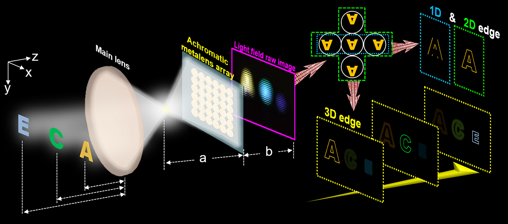
Schematic diagram of multidimensional edge detection with light-field imaging system by the achromatic meta-lens array.
3 Results and discussion
Figure 2a–d are the scanning electron microscope (SEM) images of the achromatic meta-lens array with different magnifications. The positive and negative nanostructures are specifically designed and precisely fabricated. The shape of the fabricated nanostructure slightly unmatches the ideal design due to the slight process parameter deviation. It does not deteriorate the performance of meta-lens from the experimental results. The measured focal length of the achromatic meta-lenses is 49.01 ± 0.92 µm in the working bandwidth, as shown in Figure S3. The average operation efficiency is of 38.9% which is defined as the ratio of the optical power of the focused circularly polarized beam to the power of the incident light with the opposite circular polarization.
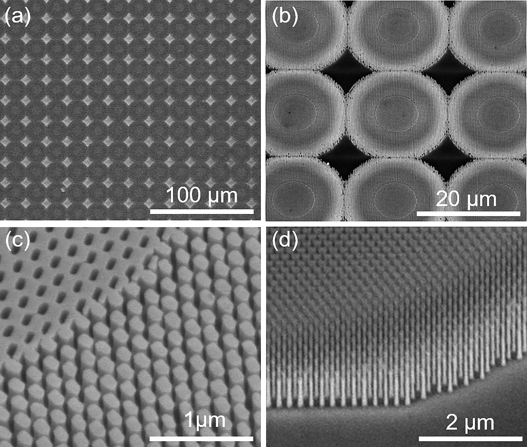
SEM images of the achromatic meta-lens array. (a) and (b) Zoomed-in SEM image of the achromatic meta-lens array. (c) and (d) Tilted-view zoomed-in SEM image of the achromatic meta-lens array. The tilted angle is 30° and 45°, respectively.
For edge detection imaging, an achromatic meta-lens array-based light-field imaging system is shown in Figure S4. Objects are illuminated by a noncoherent white light. Since the achromatic lens array is polarization sensitive, a linear polarizer (LP) and quarter wavelength plate (QWP) are used to transfer the unpolarized white light to circular polarization. The achromatic meta-lens array collects both the intensity and light field information of the objects. The light-field image is obtained by the CMOS sensor of the commercial camera. Another LP and QWP are used to remove the background noise. This light-field imaging setup with an achromatic meta-lens array enables full-color imaging as well as light-field edge detection from 1D to 3D of the objects. The experimental results of the edge detection are shown in Figure 3. Three patterns of the letter, ‘A,’ ‘C,’ and ‘E’, with the corresponding colors of yellow, green, and blue, respectively, are used as the objects placed at different locations. The light-field raw image collected through the achromatic meta-lens array by CMOS sensor displays 56 by 38 sub-images, as shown in Figure 3a. The disparity of each sub-image of the objects is derived through the surrounding sub-images with a brightness comparison. The depths are calculated using the Euclidean geometry and the disparity. The depth calculation is shown in Figure S5. In our experiments, the number of the sub-images is less than the number of the achromatic meta-lens array due to the CMOS sensor’s size. Each sub-image consists of 96 by 96 pixels. The zoomed-in image in Figure 3b shows the sub-images of various directions of the ‘E’ pattern. All directions of the object’s light ray information are comprehensively acquired. The clear sub-images show the high imaging quality by our achromatic meta-lens array. The light-field raw image is further processed for the edge detection method. Figure 3c shows the 1D edge imaging results along the x-direction focused at the ‘A’ pattern. Circle-moving the light-field raw sub-images with one pixel along x or y-direction, then subtract it with the original light-field raw image. The 1D edge information extraction is enabled by displacement of the self-subtraction. When both x- and y-directions of edge imaging processing are performed, the 2D edge information extraction can be obtained. The rendering algorithm is applied to acquire the multiple dimensions edge images. By selecting the disparity size of the sub-images, rotating 180 degrees of the selected sub-images, then join together all the selected sub-images as the reconstructed edge images at the specific depth. The light field rendering process is shown in Figure S5. According to the rendering algorithm of the light-field imaging, the disparity appears since each sub-image captures the objects from different directions. A smaller disparity value corresponds to the further distance, which can be used for depth calculation and reconstructing the focused images at different depths. The detail of the edge information extraction process is displayed in Figure S6.
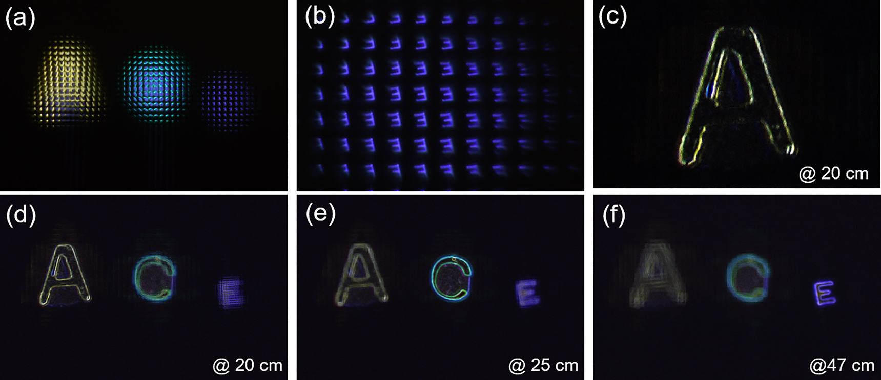
Experimental results of the edge detection light-field imaging. (a) Light field raw image formed by the achromatic meta-lens (b) the partial sub-images of the pattern ‘E’. (c) The 1D edge image along the x-direction focused on the pattern ‘A’. (d–f) The 3D edge images at different focused depths for patterns, ‘A’, ‘C’, and ‘E’.
The disparity values of the three patterns ‘A’, ‘C,’ and ‘E’ are calculated as 24, 18, and 13 pixels, respectively, as shown in Figure S7. The corresponding depths are 20 cm, 25 cm, and 47 cm for the pattern ‘A,’ ‘C,’ and ‘E,’ respectively. Figure 3d and e show the 3D edge information of the rendered images at different depths. The 3D edge imaging means the edge detection includes 2D edges at different depths. When the edge imaging is focused at 20 cm, the pattern ‘A’ has the sharpest edge. While in the other focusing depths, the edges of the pattern ‘A’ are blurred. Each pattern has the sharpest edge information while the other two letters are blurred at their corresponding depth. The results show the high-quality performance of 3D edge detection with our designed meta-lens array. (More details of the light-field imaging system, rendering algorithm, depth estimation method, 1D to 3D edge detection are discussed in Supplementary material)
We further characterized the 3D edge detection performance of the light-field system with the achromatic meta-lens array. Figure 4a shows the cut-line of the selected edges of three patterns at different depths. The edge profiles of the pattern ‘A’ at different imaging depths are shown in Figure 4b. The pattern ‘A’ is placed at 20 cm of depth, so the edge is clear at this depth than others. ‘C’ and ‘E’ have similar scenarios. The measured edge profiles in the embedded images at three corresponding depths for each pattern are shown in Figure S9. The signal-to-noise (SNR) ratios are calculated, and the SNR is defined as the ratio of the maximum signal value to the noise background value. Figure 4c shows the diagram of the measured SNR of the three patterns with three rendering depths. The SNR values of the pattern ‘A’ are 15, 7.8, and 4.2 at the depth-focused rendering of 20 cm, 25 cm, and 47 cm, respectively. At 20 cm of depth, the pattern ‘A’ has the sharpest edge with the highest SNR = 15. While in the other depths, edges of the pattern ‘A’ are blurred with lower SNR. The other two patterns, ‘C’ and ‘E’ show a similar situation. Based on the depth of patterns, the edges of the different objects can be clearly identified. It proves that focused, sharp edge images could be obtained within the broadband visible light with high quality. Our experimental results demonstrate multiple dimensional edge detection with an achromatic meta-lens array. It is quite important in imaging and sensing applications, such as 3D cell profile imaging microscopy, autonomous vehicle, advanced manufacture, etc.
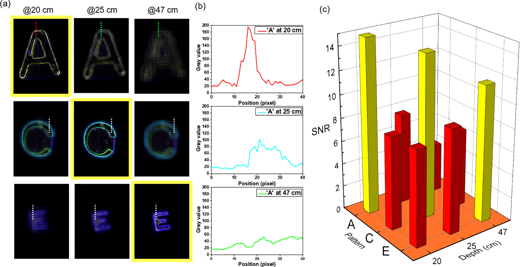
Edge sharpness measurement results of the 3D edge imaging at various depths. (a) The cut-line of the edge sharpness measurement for the SNR calculation. All the dotted lines (red, cyan, green, and white) are the selected regions for the SNR calculation. Rendered images in the same column are focused with depths of 20 cm, 25 cm, and 47 cm, respectively. (b) The edge profiles of pattern ‘A’ whose rendered images are focused with depths of 20 cm, 25 cm, and 47 cm. The color of the curve corresponds to the color of the dotted cut-line in (a). The edge profiles of the pattern ‘C’ and ‘E’ are shown in Figure S9 of Supplementary material. (c) The diagram of the measured SNR of the three patterns with three rendering depths.
4 Conclusions
We demonstrate edge detection from 1D to 3D by a light-field imaging system with an achromatic meta-lens array. The designed 60 by 60 GaN achromatic meta-lens array enables to capture of both intensity and light field information from the objects. The edge and depth of the light field information can be obtained without acquiring sectional data repeatedly. The differentiated and rendering algorithm effectively provides the boundary and the depth information of objects from 1D to 3D. This edge detection light field system has valuable advantages, such as chromatic aberration-free in the visible region, polarization selectivity, multidimensional edge detection, and the semiconductor process capability for mass production. The working band of this edge detection light field system is quite flexible. It can be tuned by changing the meta-lens array with a suitable design and fabrication. The presented 3D edge detection can improve optical characterization capabilities for applications ranging from biomedical diagnose to machine vision.
Funding source: Hong Kong Polytechnic University
Award Identifier / Grant number: 9B0Z
Award Identifier / Grant number: BBXE
Award Identifier / Grant number: BD8X
Award Identifier / Grant number: SGDX2019081623281169
Funding source: Research Grants Council, University Grants Committee
Award Identifier / Grant number: AoE/P-502/20
Funding source: Guangdong Science and Technology Department
Award Identifier / Grant number: 2020B1515120073
-
Author contribution: MKC, YY, and DPT conceived and designed the experiments. MKC designed the samples and fabricated the samples. MKC, YY, XL, YW, and DPT developed the algorithm. MKC, YY, JZ, ZZ, and JY performed optical measurement and imaging experiments. MKC, YY, and DPT prepared the manuscript. All authors analyzed the results and contributed to the preparation of the manuscript and discussions.
-
Research funding: This research was funded by the Shenzhen Science and Technology Innovation Commission Grant (No. SGDX2019081623281169), the University Grants Committee / Research Grants Council of the Hong Kong Special Administrative Region, China (Project No. AoE/P-502/20), the Department of Science and Technology of Guangdong Province (2020B1515120073), and The Hong Kong Polytechnic University (9B0Z, BBXE, and BD8X).
-
Conflict of interest statement: The authors declare no conflicts of interest regarding this article.
-
Data availability: The data that support the findings of this study are available from the corresponding author on reasonable request.
References
[1] M. Gudmundsson, E. A. El-Kwae, and M. R. Kabuka, “Edge detection in medical images using a genetic algorithm,” IEEE Trans. Med. Imaging., vol. 17, pp. 469–474, 1998.10.1109/42.712136Search in Google Scholar PubMed
[2] B. Padmapriya, T. Kesavamurthi, and H. W. Ferose, “Edge based image segmentation technique for detection and estimation of the bladder wall thickness,” Procedia Eng., vol. 30, pp. 828–835, 2012.10.1016/j.proeng.2012.01.934Search in Google Scholar
[3] N. N. S. A. Rahman, N. M. Saad, A. R. Abdullah, and N. Ahmat, “A review of vision based defect detection using image processing techniques for beverage manufacturing industry,” J. Teknol., vol. 81, pp. 33–47, 2019.10.11113/jt.v81.12505Search in Google Scholar
[4] T. H. Hou and W. L. Kuo, “A new edge detection method for automatic visual inspection,” Int. J. Adv. Manuf. Technol., vol. 13, pp. 407–412, 1997.10.1007/BF01179035Search in Google Scholar
[5] J. J. Tabor, H. M. Salis, Z. B. Simpson, et al.., “A synthetic genetic edge detection program,” Cell, vol. 137, pp. 1272–1281, 2009.10.1016/j.cell.2009.04.048Search in Google Scholar PubMed PubMed Central
[6] M. Nikolic, E. Tuba, and M. Tuba, “Edge detection in medical ultrasound images using adjusted canny edge detection algorithm,” in 24th Telecommunications Forum TELFOR, IEEE, 2016, pp. 691–694.10.1109/TELFOR.2016.7818878Search in Google Scholar
[7] C. Guo, M. Xiao, M. Minkov, Y. Shi, and S. H. Fan, “Photonic crystal slab Laplace operator for image differentiation,” Optica, vol. 5, pp. 251–256, 2018.10.1364/OPTICA.5.000251Search in Google Scholar
[8] H. Kwon, D. Sounas, A. Cordaro, A. Polman, and A. Alu, “Nonlocal metasurfaces for optical signal processing,” Phys. Rev. Lett., vol. 121, p. 173004, 2018.10.1103/PhysRevLett.121.173004Search in Google Scholar PubMed
[9] Q. He, F. Zhang, M. Pu, et al.., “Monolithic metasurface spatial differentiator enabled by asymmetric photonic spin-orbit interactions,” Nanophotonics, vol. 1, pp. 741–748, 2020.10.1515/9783110710687-062Search in Google Scholar
[10] J. Zhou, H. Qian, J. Zhao, et al.., “Two-dimensional optical spatial differentiation and high-contrast imaging,” Natl. Sci. Rev., vol. 8, pp. 1–8, 2020.10.1093/nsr/nwaa176Search in Google Scholar PubMed PubMed Central
[11] J. X. Zhou, H. L. Qian, C. F. Chen, et al.., “Optical edge detection based on high-efficiency dielectric metasurface,” Proc. Natl. Acad. Sci. U. S. A., vol. 116, pp. 11137–11140, 2019.10.1073/pnas.1820636116Search in Google Scholar PubMed PubMed Central
[12] Y. Zhou, W. H. Wu, R. Chen, W. J. Chen, R. P. Chen, and Y. G. Ma, “Analog optical spatial differentiators based on dielectric metasurfaces,” Adv. Opt. Mater., vol. 8, p. 1901523, 2020.10.1002/adom.201901523Search in Google Scholar
[13] Y. Zhou, H. Y. Zheng, I. I. Kravchenko, and J. Valentine, “Flat optics for image differentiation,” Nat. Photonics, vol. 14, pp. 316–323, 2020.10.1038/s41566-020-0591-3Search in Google Scholar
[14] L. Wan, D. P. Pan, S. F. Yang, et al.., “Optical analog computing of spatial differentiation and edge detection with dielectric metasurfaces,” Opt. Lett., vol. 45, pp. 2070–2073, 2020.10.1364/OL.386986Search in Google Scholar PubMed
[15] M. L. Ren Ng, M. Brédif, G. Duval, M. Horowitz, and P. Hanrahan, “Light field photography with a hand-held plenoptic camera,” CS Tech. Rep., 2005, CSTR 2005-02.Search in Google Scholar
[16] P. Nussbaum, R. Volke, H. P. Herzig, M. Eisner, and S. Haselbeck, “Design, fabrication and testing of microlens arrays for sensors and microsystems,” Pure Appl. Opt., vol. 6, pp. 617–636, 1997.10.1088/0963-9659/6/6/004Search in Google Scholar
[17] S. M. Choudhury, D. Wang, K. Chaudhuri, et al.., “Material platforms for optical metasurfaces,” Nanophotonics, vol. 7, pp. 959–987, 2018.10.1515/nanoph-2017-0130Search in Google Scholar
[18] S. Jahani and Z. Jacob, “All-dielectric metamaterials,” Nat. Nanotechnol., vol. 11, pp. 23–36, 2016.10.1038/nnano.2015.304Search in Google Scholar PubMed
[19] A. Schirato, M. Maiuri, A. Toma, et al.., “Transient optical symmetry breaking for ultrafast broadband dichroism in plasmonic metasurfaces,” Nat. Photonics, vol. 14, pp. 723–727, 2020.10.1038/s41566-020-00702-wSearch in Google Scholar
[20] G. K. Shirmanesh, R. Sokhoyan, P. C. Wu, and H. A. Atwater, “Electro-optically tunable multifunctional metasurfaces,” ACS Nano, vol. 14, pp. 6912–6920, 2020.10.1021/acsnano.0c01269Search in Google Scholar PubMed
[21] I. Staude, T. Pertsch, and Y. S. Kivshar, “All-dielectric resonant meta-optics lightens up,” ACS Photonics, vol. 6, pp. 802–814, 2019.10.1021/acsphotonics.8b01326Search in Google Scholar
[22] F. Yang, P. A. Huidobro, and J. B. Pendry, “Transformation optics approach to singular metasurfaces,” Phys. Rev. B, vol. 98, p. 125409, 2018.10.1103/PhysRevB.98.125409Search in Google Scholar
[23] D. S. Zhang, B. Ranjan, T. Tanaka, and K. Sugioka, “Carbonized hybrid micro/nanostructured metasurfaces produced by femtosecond laser ablation in organic solvents for biomimetic antireflective surfaces,” ACS Appl. Nano Mater., vol. 3, pp. 1855–1871, 2020.10.1021/acsanm.9b02520Search in Google Scholar
[24] X. F. Zang, F. L. Dong, F. Y. Yue, et al.., “Polarization encoded color image embedded in a dielectric metasurface,” Adv. Mater., vol. 30, 2018, Art no. 1707499.10.1002/adma.201707499Search in Google Scholar PubMed
[25] J. T. Hu, D. Q. Wang, D. Bhowmik, et al.., “Lattice-resonance metalenses for fully reconfigurable imaging,” ACS Nano, vol. 13, pp. 4613–4620, 2019.10.1021/acsnano.9b00651Search in Google Scholar PubMed
[26] D. J. Roth, M. K. Jin, A. E. Minovich, S. Liu, G. X. Li, and A. V. Zayats, “3D full-color image projection based on reflective metasurfaces under incoherent illumination,” Nano Lett., vol. 20, pp. 4481–4486, 2020.10.1021/acs.nanolett.0c01273Search in Google Scholar PubMed
[27] X. Li, L. W. Chen, Y. Li, et al.., “Multicolor 3D meta-holography by broadband plasmonic modulation,” Sci. Adv., vol. 2, 2016, Art no. e1601102.10.1126/sciadv.1601102Search in Google Scholar PubMed PubMed Central
[28] D. Wang, F. Liu, T. Liu, S. Sun, Q. He, and L. Zhou, “Efficient generation of complex vectorial optical fields with metasurfaces,” Light Sci. Appl., vol. 10, pp. 1–14, 2021.10.1038/s41377-021-00504-xSearch in Google Scholar PubMed PubMed Central
[29] Q. Cheng, J. Wang, L. Ma, et al.., “Achromatic terahertz airy beam generation with dielectric metasurfaces,” Nanophotonics, vol. 1, pp. 1123–1131, 2020.10.1515/nanoph-2020-0536Search in Google Scholar
[30] K. Koshelev, S. Kruk, E. Melik-Gaykazyan, et al.., “Subwavelength dielectric resonators for nonlinear nanophotonics,” Science, vol. 367, pp. 288–292, 2020.10.1126/science.aaz3985Search in Google Scholar PubMed
[31] F. Zhang, M. Pu, X. Li, et al.., “All‐dielectric metasurfaces for simultaneous giant circular asymmetric transmission and wavefront shaping based on asymmetric photonic spin–orbit interactions,” Adv. Funct. Mater., vol. 27, 2017, Art no. 1704295.10.1002/adfm.201704295Search in Google Scholar
[32] Q. Fan, M. Liu, C. Zhang, et al.., “Independent amplitude control of arbitrary orthogonal states of polarization via dielectric metasurfaces,” Phys. Rev. Lett., vol. 125, p. 267402, 2020.10.1103/PhysRevLett.125.267402Search in Google Scholar PubMed PubMed Central
[33] Y. Deng, M. Wang, Y. Zhuang, S. Liu, W. Huang, and Q. Zhao, “Circularly polarized luminescence from organic micro-/nano-structures,” Light Sci. Appl., vol. 10, pp. 1–18, 2021.10.1038/s41377-021-00516-7Search in Google Scholar PubMed PubMed Central
[34] M. X. Zhao, M. K. Chen, Z. P. Zhuang, et al.., “Phase characterisation of metalenses,” Light Sci. Appl., vol. 10, p. 52, 2021.10.1038/s41377-021-00492-ySearch in Google Scholar PubMed PubMed Central
[35] N. F. Yu, P. Genevet, M. A. Kats, et al.., “Light propagation with phase discontinuities: generalized laws of reflection and refraction,” Science, vol. 334, pp. 333–337, 2011.10.1126/science.1210713Search in Google Scholar PubMed
[36] M. K. Chen, Y. Wu, L. Feng, et al.., “Principles, functions, and applications of optical meta‐lens,” Adv. Opt. Mater., vol. 9, 2021, Art no. 2001414.10.1002/adom.202001414Search in Google Scholar
[37] L. Li, Z. X. Liu, X. F. Ren, et al.., “Metalens-array-based high-dimensional and multiphoton quantum source,” Science, vol. 368, pp. 1487–1490, 2020.10.1126/science.aba9779Search in Google Scholar PubMed
[38] M. M. Li, S. S. Li, L. K. Chin, Y. F. Yu, D. P. Tsai, and R. S. Chen, “Dual-layer achromatic metalens design with an effective Abbe number,” Opt Express, vol. 28, pp. 26041–26055, 2020.10.1364/OE.402478Search in Google Scholar PubMed
[39] S. M. Wang, P. C. Wu, V. C. Su, et al.., “A broadband achromatic metalens in the visible,” Nat. Nanotechnol., vol. 13, pp. 227–232, 2018.10.1038/s41565-017-0052-4Search in Google Scholar PubMed
[40] S. M. Wang, P. C. Wu, V. C. Su, et al.., “Broadband achromatic optical metasurface devices,” Nat. Commun., vol. 8, p. 187, 2017.10.1038/s41467-017-00166-7Search in Google Scholar PubMed PubMed Central
[41] R. J. Lin, V. C. Su, S. M. Wang, et al.., “Achromatic metalens array for full-colour light-field imaging,” Nat. Nanotechnol., vol. 14, pp. 227–231, 2019.10.1038/s41565-018-0347-0Search in Google Scholar PubMed
[42] H. H. Hsiao, Y. H. Chen, R. J. Lin, et al.., “Integrated resonant unit of metasurfaces for broadband efficiency and phase manipulation,” Adv. Opt. Mater., vol. 6, 2018, Art no. 1800031.10.1002/adom.201800031Search in Google Scholar
Supplementary Material
The online version of this article offers supplementary material (https://doi.org/10.1515/nanoph-2021-0239).
© 2021 Mu Ku Chen et al., published by De Gruyter, Berlin/Boston
This work is licensed under the Creative Commons Attribution 4.0 International License.
Articles in the same Issue
- Frontmatter
- Editorial
- A tribute to Mark Stockman
- Perspectives
- Plasmons compressing the light – a jewel in the treasure chest of Mark Stockman’s legacy
- Novel non-plasmonic nanolasers empowered by topology and interference effects
- Nanofocusing: reaching out
- Spaser or plasmonic nanolaser? – Reminiscences of discussions and arguments with Mark Stockman
- Plasmonic nanolasers: fundamental properties and applications
- Research Articles
- Space- and time-resolved second harmonic spectroscopy of coupled plasmonic nanocavities
- Surface-response functions obtained from equilibrium electron-density profiles
- Effect of nanoscale dielectric environments on concentration quenching
- Optical spin–orbit coupling in the presence of magnetization: photonic skyrmion interaction with magnetic domains
- Anomalous ultrafast all-optical Hall effect in gapped graphene
- Exploiting space-time duality in the synthesis of impedance transformers via temporal metamaterials
- Optical current generation in graphene: CEP control vs. ω + 2ω control
- Edge detection with meta-lens: from one dimension to three dimensions
- Coherent control at gold needle tips approaching the strong-field regime
- Tailoring exceptional points in a hybrid PT-symmetric and anti-PT-symmetric scattering system
- Transition to strong coupling regime in hybrid plasmonic systems: exciton-induced transparency and Fano interference
- Single-nanoantenna driven nanoscale control of the VO2 insulator to metal transition
- High laser induced damage threshold photoresists for nano-imprint and 3D multi-photon lithography
- Onset of charge interaction in strong-field photoemission from nanometric needle tips
- Massive surface-plasmon polaritons
- VCSEL with multi-transverse cavities with bandwidth beyond 100 GHz