Preparation and properties of plasmonic-excitonic nanoparticle assemblies
-
Brian Szychowski


Abstract
The assembly of inorganic nanoparticles often leads to collective properties that are different from the combined properties of the individual components. In particular, coupling plasmonic and excitonic nanoparticles has been shown to modify their optical properties, including absorption, emission, and scattering. Because of this, these coupled assemblies have potential applications in a wide range of areas, including sensing, light harvesting, and photocatalysis. More recently, unique properties, including Fano interference and Rabi splitting, have been observed by increasing the coupling strength. However, the behavior of coupled nanoparticles is highly dependent on the exact organization of the components, including the number of particles coupled, the distance separating them, and their spatial orientation. This is especially true in the case of strongly coupled particles. Because of this, it is important to achieve synthetic techniques that not only can link particles together but also offer good control over how the particles are connected. In this review, assemblies of plasmonic and excitonic nanoparticles are reviewed, including the various methods that have been used for their construction, the properties that these systems have been predicted to possess as well as the ones that have been observed, and their current applications along with current challenges in the field and potential future applications.
1 Introduction
Inorganic nanoparticles have been the subject of numerous studies and have been used in a wide range of applications in recent years, including as sensors [1], bioimaging agents [2], catalysts [3], and light-emitting devices [4], among others. Inorganic nanoparticles consist of inorganic materials having at least one dimension less than 100 nm. Inorganic nanoparticles are broadly classified as plasmonic [5], semiconductor [6], magnetic [7], or lanthanide [8] based on the material they are composed of and the physical properties they display. More recently, nanocomposites containing parts from two or more of these classes have been developed. This review will focus on assemblies made from two types of inorganic nanoparticles: plasmonic nanoparticles (PNPs) and semiconductor nanocrystals [or quantum dots (QDs)].
PNPs are characterized by their ability to support localized surface plasmons, that is, collective oscillations of the free electrons in the material that can couple to incident electromagnetic radiation. Gold nanoparticles (AuNPs) are the most commonly studied PNPs because they support strong localized surface plasmons at optical frequencies and because of the synthetic methods that are available. AuNPs were discovered by Faraday more than 150 years ago. However, the first widely explored synthetic method was developed by Turkevich et al. in the 1950s [9]. Since then, other methods have been reported for the preparation of PNPs of different sizes (<1 to >100 nm) [10], [11], metals (silver [12] and platinum [13]), and shapes (rods [14], stars [15], and prisms [16]). The properties of PNPs are highly dependent on a variety of factors, including material, size, shape, and local refractive index; thus, the extensive synthetic methods that have been developed allow for the fine-tuning of these properties. PNPs are highly efficient scatterers and absorbers of light (due to high electron density), have low toxicity, and possess easily modified surface chemistry. These properties have made PNPs useful for applications, including sensors [17], bioimaging agents [2], drug delivery systems [18], and surface-enhanced Raman spectroscopy (SERS) [19].
In contrast to PNPs, the fundamental excitation in semiconductor nanocrystals is an exciton or electron-hole pair. Excitation by light sends an electron from the valence band to the conduction band, leaving behind a hole. The recombination of the electron-hole pair releases energy, as either heat or fluorescence, and the fluorescence quantum yields of QDs can be high. Thus, although both PNPs and QDs have sizes in the nanoscale, their optical properties differ drastically. Furthermore, similar to the wavelength of surface plasmon resonance in PNPs, the wavelength of absorption and emission of QDs is dependent on the material, shape, and size of the QDs and can therefore be tuned to a wide spectrum. As in the case of PNPs, QDs have found applications as biomarkers as well as in energy harvesting and storage, quantum information, photonics, and light-emitting devices [4], [20]. Compared to organic dyes, semiconductor QDs possess good photostability, wide excitation and narrow emission bandwidths, large absorption cross-sections, high quantum yields, and size-dependent emission wavelengths [4], [21], [22], [23].
The controlled organization and assembly of nanoparticles – in both small, well-controlled clusters and larger, microscale arrays – is of importance. This is because the excitations (plasmons or excitons) of nearby nanoparticles interact with each other in a distance-dependent manner; therefore, controlling the spacing and orientation of particles is important for controlling the properties of the nanoparticle assembly. However, arranging nanoparticles in controlled ways poses challenges. Controlling the specific distance between particles can be accomplished through varying the size and/or thickness of the ligands attached to the particles. However, controlling the size of clusters (the number of particles they contain) and spatial orientation of nanoparticles within the clusters is more difficult. Attempts to create discrete assemblies of two or more nanoparticles generally result in the formation of assemblies of several different sizes, which are then challenging to separate. Different techniques used to assemble PNPs have been investigated and reviewed by Grzelczak et al. [24] and Gwo et al. [25].
The assembly of two different types of nanoparticles (in this case, plasmonic and semiconductor) is also of interest. Combining plasmonic and semiconductor nanoparticles into a single system results in an interaction between the plasmon and exciton, which can greatly influence the existing properties of the particles or lead to entirely new properties different from either of the particles on their own. Because this interaction is dependent on factors such as interparticle separation, orientation, and relative concentrations, it is important to be able to assemble PNPs and semiconductor QDs in a controlled fashion. However, controlling these factors is not trivial.
In this review, heteronanoparticle assemblies consisting of PNPs and QDs (PNP-QD hybrids) are discussed, with a focus on the synthetic strategies used to prepare such assemblies. It should be noted that single particles can also contain domains of two or more distinct materials (for example, core-shell or tipped structures), and the synthesis and properties of these types of hybrid nanoparticles have been reviewed by Jiang et al. [26] and Costi et al. [27]. Additionally, plasmon-exciton coupling has been reported using lithographically defined plasmonic arrays with layers of semiconductor materials [28], [29]. However, this review is solely focused on the formation of assemblies made by linking two or more discrete, distinct nanoparticles. Synthetic methods will first be reviewed in two parts: solution-based approaches and substrate-based techniques. Next, the properties of PNP-QD assemblies will be covered. Finally, there will be a discussion of the applications thus far and future directions for the field.
2 Solution-based synthetic methods
While perhaps the simplest means of achieving PNP-QD hybrid assemblies, solution-based methods come with limitations, namely, controlling the process to obtain the desired arrangements without forming unwanted side products. This results in low reproducibility and generally low yields [30]. Nevertheless, a wide variety of techniques have been used to synthesize PNP-QD hybrid assemblies in solution, including covalent linking of small molecules or biomolecules [1], [31], DNA hybridization [32], [33], [34], [35], and self-assembly [36], [37], [38], [39], [40].
2.1 Covalent linking
For covalent binding through small molecules, PNPs and QDs are coated with ligands terminated with reactive functional groups. After mixing, the functional groups are reacted to form a covalent bond, such as an amide [41], imine [42], or disulfide bond [30]. Because of the wide range of small molecules available with different lengths and functional groups, the covalent binding of small molecules is perhaps the most versatile technique. However, it is difficult to control the number and arrangement of the nanoparticles that bind to one another.
Aldeek et al. [41] used established 1-ethyl-3-(dimethylaminopropyl)carbodiimide (EDC) coupling to link CdSe/ZnS core-shell QDs to small AuNPs. The QDs were made water soluble through functionalization with a polyethylene glycol (PEG) ligand terminated by dihydrolipoic acid on one end (to bind to the QD surface) and an amine functional group at the other end. AuNPs were functionalized with a similar PEG molecule terminated by lipoic acid and carboxylic acid groups, which were then activated using EDC and N-hydroxysuccinimide (NHS). The ligands of the QDs and AuNPs were then reacted together to form an amide bond. To control the extent of the linking between particles, the surface of the QDs was 95% passivated with an inert PEG ligand containing a methoxy group in place of an amine. Although no studies were done to characterize the number of QDs coupled, the quenching of QD fluorescence was evidence that the QDs had coupled to the AuNPs.
EDC coupling was also used to couple AuNPs and CdSe/ZnS QDs with the aid of a peptide linker [43]. The carboxyl functionalized QDs were activated with EDC and reacted with the N terminus of the peptide; a cysteine at the C terminus was available to bind to the surface of added AuNPs. A similar procedure was developed, where AuNPs and QDs were both attached to polystyrene beads, which helped prevent the aggregation of the QDs [44].
Maneeprakorn et al. [42] also used the formation of amide bonds to link AuNPs and silver nanoparticles (AgNPs) with CdS and CdSe QDs, wherein the QDs were functionalized with 11-mercaptoundecanoyl chloride and the PNPs with 4-aminothiophenol. Equally as effective was an azo linkage, performed by functionalizing the QDs instead with 4-aminothiophenol and then converting it to a diazonium group (Figure 1). In both cases, they found that a degree of control of the reaction could be obtained using a syringe pump to add one component to the other slowly and in large excess. By varying the reaction conditions, it was possible to obtain QDs surrounded by one, two, three, or four PNPs. Images of the types of arrangements formed are shown in Figure 1.
![Figure 1: Covalent linkage of AuNPs and CdS QDs.(A–E) Structures formed by assembling AuNPs and CdS QDs. (A) A dimer of one AuNP and one QD. (B) Two dimers of one AuNP and one QD. (C) Trimer of one QD between two AuNPs. (D) Tetramer of one QD between three AuNPs. (E) Pentamer of one QD surrounded by four AuNPs. (F) Reaction scheme depicting the linking of AuNPs and CdS QDs through the formation of an azo bond. Adapted with permission from Ref. [42]. Copyright 2010 American Chemical Society.](/document/doi/10.1515/nanoph-2018-0168/asset/graphic/j_nanoph-2018-0168_fig_001.jpg)
Covalent linkage of AuNPs and CdS QDs.
(A–E) Structures formed by assembling AuNPs and CdS QDs. (A) A dimer of one AuNP and one QD. (B) Two dimers of one AuNP and one QD. (C) Trimer of one QD between two AuNPs. (D) Tetramer of one QD between three AuNPs. (E) Pentamer of one QD surrounded by four AuNPs. (F) Reaction scheme depicting the linking of AuNPs and CdS QDs through the formation of an azo bond. Adapted with permission from Ref. [42]. Copyright 2010 American Chemical Society.
Similarly, Nepal et al. [30] also found that a lower reaction concentration helped control the linking process. In this case, QDs were attached to gold nanorods (AuNRs) through their functionalization with amine-terminated ligands, which were subsequently converted to thiols using Traut’s reagent, and finally linked via the creation of a disulfide bond. Increasing the concentration of nanoparticles in solution from 0.2 to 2 nm resulted in a higher distribution in the number of QDs bound to each rod. Further control was obtained through the selective functionalization of the ends of the AuNRs. Under optimal conditions (1:1 molar ratio AuNR/QD, 0.2 nm, room temperature), the reaction was able to yield 70% rods with singly bound QDs, with only 2% of the QDs remaining unbound.
2.2 Biomolecular linking
Compared to linking using small molecules, linking with DNA offers several advantages. First, DNA can be tailored to specific lengths by varying the number of base pairs [32]. Additionally, the double-helix structure of DNA is fairly rigid, allowing for the precise control of the spacing [33]. Finally, techniques exist, which can be used to obtain nanoparticles with one and only one strand of DNA attached [34], [35], enabling fine control over the organization of assemblies. However, because of the size of DNA compared to small molecules, separation is limited to distances greater than 6 nm [33]. Further, DNA must be kept at conditions under which it is stable, limiting the conditions under which this technique can be used. DNA hybridization has been used to link QDs to AuNPs of different sizes (from 1.4 nm [33] to 80 nm [45]) and in different conformations (QD-AuNP dimmers [33], tetramers of three AuNPs with one QD [46], AuNP surrounded by QDs or QD surrounded by AuNPs [47]) and to form superlattice networks of AuNPs and QDs [32].
To link the nanoparticles through DNA hybridization, both the PNPs and the QDs must be functionalized with single-stranded DNA (ssDNA) [48]. In the case of PNPs, this is typically accomplished through the direct addition of thiol-terminated DNA [32]. For QDs, the direct addition of DNA is not used due to issues with QD water solubility [45]. Instead, QDs must first be made water soluble. This is done through ligand exchange using carboxylate molecules such as DHLA [47] or mercaptopropionic acid (MPA) [45], or precoating QDs with carboxy-containing polymers [32], which can then be EDC coupled with DNA. Another rather common strategy is to use DNA terminated with a hexahistidine moiety to attach the DNA to the surface of the QD [46], [47], [49] due to a strong interaction between the hexahistidine and the surface of the QDs [50].
The use of DNA allows for the use of techniques that can isolate monovalent nanoparticles from multivalent ones. Relying on the negative charge of DNA, gel electrophoresis has been used in the past to isolate monovalent AuNPs [51], and this technique has been used in conjunction with hybridization to ssDNA-functionalized QDs to give the controlled formation of dimers, trimers, and other small groupings of AuNPs and QDs with yields as high as 65% [46]. A collection of the types of structures assembled with this method is shown in Figure 2. In a similar manner, magnetic beads have been used to obtain monovalent QDs [35]. In this study, QD-ssDNA were first hybridized onto magnetic beads. The magnetic beads were then rinsed with solutions of varying ionic strengths, which were able to release the QD-ssDNA based on the number of strands attached. This was used to obtain a solution containing 93% monovalent QDs, which could then be coupled with a single AuNP.
![Figure 2: Depiction and corresponding TEM images of structures formed from AuNPs functionalized with ssDNA strands that are then hybridized with QDs.(A) AuNP functionalized with many strands of ssDNA. (B) AuNP functionalized with a single ssDNA strand and then hybridized with ssDNA functionalized QDs. (C) Trimer formed between two singly functionalized AuNPs linked to a QD. Adapted from Ref. [52]. Copyright 2012 American Chemical Society.](/document/doi/10.1515/nanoph-2018-0168/asset/graphic/j_nanoph-2018-0168_fig_002.jpg)
Depiction and corresponding TEM images of structures formed from AuNPs functionalized with ssDNA strands that are then hybridized with QDs.
(A) AuNP functionalized with many strands of ssDNA. (B) AuNP functionalized with a single ssDNA strand and then hybridized with ssDNA functionalized QDs. (C) Trimer formed between two singly functionalized AuNPs linked to a QD. Adapted from Ref. [52]. Copyright 2012 American Chemical Society.
The technique of DNA origami has been used by the Liedl group to obtain better control over the coupling process [53]. In DNA origami, a relatively long single strand of DNA is engineered, which can be carefully folded into specific conformations through the addition of shorter nucleotide chains. This technique was used to give a base structure of DNA with binding sites at specific locations; these binding sites then selectively bind AuNPs or CdTe QDs hybridized with a complementary strand of DNA. The general shape of the obtained structures consisted of a core particle surrounded by arms containing satellites; the satellites in this study were either smaller AuNPs, CdTe QDs, or organic dyes. By changing the DNA origami structure, they were able to vary the length and number of arms, the number of satellites per arm, and even the arrangement of the satellites on the arm (for example, in a straight line vs. twisting around the arm in a helical pattern) with remarkable precision (depending on the size of the core particle and the deviation in the number of satellites that ranged from 6% to 17%). Other DNA origami templates were also used to arrange AuNPs and with CdTe/CdS QDs into dimers with nanometer precision over separation distance [54] and to prepare groupings of AuNPs with one, two, or three CdSe/ZnS QDs with the desired structures produced in 80% yield [55]. Although more complicated than standard DNA hybridization, DNA origami allows for the construction of more complex arrangements of nanoparticles with high precision.
The use of hexahistidine as an anchoring moiety to the surface of QDs has been discussed above, in conjunction with DNA, but this moiety can also be conjugated to a larger peptide to facilitate the coupling of PNPs and QDs. For example, a peptide that has a hexahistidine at one end and a dicysteine at the other has been used; this peptide was first mixed with AuNPs, using its dicysteine end to interact with the gold surface, and then the hexahistidine end enabled nanoparticle crosslinking (or bridging) by adsorption onto the surface of the added QDs [31]. Another experiment used the hexahistidine group, covalently linked to PEG-stabilized CdS-ZnS QDs, to coordinate with nickel, deposited on the surface of AuNPs using Ni-nitrilotriacetate [56].
Similarly, proteins with affinity for each other have been used for the coupling of PNPs and QDs [57], [58], [59], [60], [61], [62], [63], [64], [65], [66], [67]. The biotin/streptavidin complex is the most commonly used due to the well-known affinity between these two partners [57] as well as the availability of commercial CdSe-ZnS core-shell QDs functionalized with streptavidin [52]. To use these streptavidin-QDs, the PNPs must be functionalized with biotin. This is commonly done through EDC coupling, where the PNP is functionalized with an amine-terminated ligand. For example, 3 nm AuNPs were coated with polyamidoamine dendrimer, which was then reacted with sulfo-NHS-biotin to functionalize the surface of the AuNPs with biotin [57]. This led to the formation of clusters consisting of a QD surrounded by multiple AuNPs. A similar experiment was performed, which resulted in the coupling of AgNPs with the same commercially available CdSe/ZnS core-shell QDs [58].
Although many of the previously discussed experiments resulted in a single central nanoparticle surrounded by many other nanoparticles, a similar experiment was done using biotin-streptavadin, which was able to give controlled, discrete groupings [52]. In this report, biotinylated DNA was attached to 80 nm AuNPs using a thiolated DNA linker. The biotinylated AuNPs were then reacted with streptavidin-QDs in varying ratios: 1:1, 2:1, or 100:1 QD/AuNP ratio; these gave a single QD attached to an AuNP, a QD between two AuNPs, or an AuNP surrounded by QDs, respectively. Once synthesized, the desired structure could be isolated from the resulting mixture using gel electrophoresis.
The Kotov laboratory has also done extensive work using biotin-streptavidin binding to attach PNPs to the surface of CdTe nanowires [60], [61], [62]. Cysteine-stabilized CdTe nanowires were reacted with sulfo-NHS-biotin to attach biotin to the surface of the nanowires. Similarly, AuNPs stabilized with MPA were activated with EDC/sulfo-NHS and then coupled with streptavidin. The CdTe nanowires and AuNPs were then mixed in varying ratios. Because the CdTe nanowires are so large relative to the AuNPs (3 nm AuNPs vs. 6×1027 nm CdTe), AuNPs were used in 500–1000 times excess. This resulted in the AuNPs forming a cylindrical outer “shell” around the exterior of the CdTe nanowires, with a spacing equal to the thickness of the biotin-streptavidin complex in between [61]. A similar experiment was performed, which created a shell of AgNPs surrounding CdTe nanowires of similar size [60].
This structure was further developed into a “molecular spring”, a structure capable of reversible shifts in absorption wavelength [62]. In this case, PEGylated anti-streptavidin antibody (aB) was used as the crosslinking agent in place of biotin and streptavidin. A two-step conjugation process was used to reduce the possibility of crosslinking between CdTe nanowires. First, amine-functionalized AuNPs were reacted with NHS-CO-PEG-NH-di-tert-butyl dicarbonate (t-BOC) to form an amide bond. Here, t-BOC acts as a protecting group to prevent unwanted reactivity between the AuNPs. The t-BOC group was then removed using trifluoroacetic acid, and the newly revealed amine was attached to anti-streptavidin through EDC coupling. The same PEG molecule was attached to the surface of the CdTe nanowires and then coupled to the AuNP-bound anti-streptavidin following the same procedure to give an AuNP-PEG-aB-PEG-CdTe structure. The reversible binding of a complementary antigen by the anti-streptavidin resulted in an increase of the separation distance between the nanowire and the QDs and a corresponding shift in the absorption spectrum.
Bovine serum albumin (BSA) is another protein that has been used for the assembly of PNPs and QDs, wherein both nanoparticles are attached to, and separated by, BSA [63], [64], [65]. This can be done through the covalent attachment of the protein to the nanoparticles coatings, as explained in the cases of biotin above. AuNPs were first synthesized in the presence of BSA through sodium borohydride reduction, resulting in BSA-stabilized AuNPs, to which MPA-functionalized CdSe QDs were added; the EDC coupling of the MPA ligands of QDs to the BSA resulted in AuNPs surrounded by QDs at a distance of approximately 10 nm, the size of BSA [64]. The scheme of this reaction and a transmission electron microscopy (TEM) image of the assembled structure are shown in Figure 3. Because it contains a large amount of charge at neutral pH [63], BSA can also interact with nanoparticles through charge interactions. This can be achieved through direct interaction with the surface of the nanoparticle [63] or through electrostatic interactions with the ligands attached to the particle; for example, with the positively charged ligand cetyl-trimethyl ammonium bromide (CTAB), which was used to coat AuNRs with CdSe-ZnS core-shell QDs [65]. This can also be viewed as a form of self-assembly, which will be the last class of solution-based assembly technique discussed.
![Figure 3: Biomolecular linking of AuNPs and CdSe QDs.(A) Reaction scheme linking CdSe QDs to BSA functionalized AuNPs through EDC coupling. (B) TEM image depicting an AuNP linked to CdSe QDs through BSA. Adapted from Ref. [64]. Copyright 2010 American Chemical Society.](/document/doi/10.1515/nanoph-2018-0168/asset/graphic/j_nanoph-2018-0168_fig_003.jpg)
Biomolecular linking of AuNPs and CdSe QDs.
(A) Reaction scheme linking CdSe QDs to BSA functionalized AuNPs through EDC coupling. (B) TEM image depicting an AuNP linked to CdSe QDs through BSA. Adapted from Ref. [64]. Copyright 2010 American Chemical Society.
2.3 Self-assembly
The self-assembly of nanoparticles occurs when nanoparticles assemble simply by mixing them, either owing to some intrinsic property of the nanoparticles or due to interactions of the ligands attached to them. Self-assembly can occur through electrostatic attraction [36], [37], [68], [69], [70], ligand exchange [3], [21], [38], [39], [40], or hydrophobic or other interactions [70], [71], [72]. No additional chemistry after mixing is required. Because of this, self-assembly is perhaps the most straightforward of all the techniques established to form PNP-QD assemblies. However, because there are no additional steps required, it is challenging to obtain control over the assembly process. As such, self-assembly is primarily useful for the formation of assemblies where one type of particle is added in large excess and ends up completely surrounding the other [3], [36], [68], [70] or where equal mixing leads to the formation of a large network of interconnected particles [38], [39]. These two possibilities are illustrated in Figure 4A.
![Figure 4: Self-assembly of AuNPs and CdS QDs.(A) Schematic depicting two possible self-assembly routes: a 1:10 ratio of oppositely charged nanoparticles, which leads to isolated particles surrounded by a layer of oppositely charged particles, or a 1:1 ratio, which leads to a large interconnected network. (B–E) High-resolution TEM images depicting AuNPs with a layer of CdS QDs coating the surface. Adapted with permission from Ref. [36]. Copyright 2002 American Chemical Society.](/document/doi/10.1515/nanoph-2018-0168/asset/graphic/j_nanoph-2018-0168_fig_004.jpg)
Self-assembly of AuNPs and CdS QDs.
(A) Schematic depicting two possible self-assembly routes: a 1:10 ratio of oppositely charged nanoparticles, which leads to isolated particles surrounded by a layer of oppositely charged particles, or a 1:1 ratio, which leads to a large interconnected network. (B–E) High-resolution TEM images depicting AuNPs with a layer of CdS QDs coating the surface. Adapted with permission from Ref. [36]. Copyright 2002 American Chemical Society.
For electrostatically induced self-assembly, the PNP and QD must be functionalized with oppositely charged ligands. For example, Wargnier et al. [37] used carboxy-functionalized AuNPs mixed with cysteamine-coated CdSe/ZnS core-shell QDs. Kolny et al. [36] mixed MPA-coated AuNPs with (diethylamino)ethanethiol-stabilized CdSe-ZnS QDs in a molar ratio of 1:100 and were able to obtain AuNPs surrounded by a layer of QDs. The resulting AuNP-QD structure is depicted in Figure 4.
A more complex assembly was undertaken by the Kotov group using positively charged CTAB-stabilized AuNRs and negatively charged cysteine-stabilized CdTe QDs [68]. Mixing at high ratios (180 QDs/1 AuNRs) led to the formation of monomeric AuNRs surrounded by QDs. Similar results were obtained with spherical particles. However, lower ratios (15:1) led to the formation of AuNR dimers arranged side-to-side with a layer of CdTe QDs in between. This structure was seen in 70% of the observed particles. The same side-by-side assembly of AuNRs was reported when negatively charged citrate ions were introduced due to a loss of electrostatic stabilization of the AuNRs [73], [74]. Furthermore, the assembled structures retained a chiral character when chiral cysteine was used to coat the CdTe QDs.
Self-assembly can also be achieved by relying on ligand exchange to bridge the nanoparticles. This provides a more rugged connection than electrostatic self-assembly and can also lead to a slightly better control over the spacing and structure of the assembly. As with electrostatic self-assembly, high ratios can lead to discrete assemblies, whereas lower ratios will lead to the formation of larger networks of particles [39].
Cumberland et al. [38] formed a nanocomposite several micrometers in size by mixing AuNPs and CdSe QDs of similar sizes (~6 nm). The CdSe QDs were coated with aminoethanethiol, with the thiol group anchored to the surface of the QD. The free amine was then able to displace the citrate ions stabilizing the AuNPs due to its higher affinity with gold, which led to crosslinking between the two types of nanoparticles. Interestingly, scanning electron microscopy (SEM) energy-dispersive X-ray spectroscopy (EDS) found approximately the same element amounts (1:6 gold/CdSe) regardless of the initial ratio of nanoparticles used. Although this may seem contrary to other studies, which found that a large excess leads to a saturation of the surface of one of the types of nanoparticles by the other, it should be noted that the CdSe QDs (here in up to 60 times excess) were added to the AuNPs slowly and that the AuNPs were of the same size as the QDs. As such, even when large excess of CdSe QDs were used, it is expected that networks would form before saturation of the AuNPs could occur.
Block copolymers have been used as the ligands to facilitate thiol-based self-assembly. QDs were functionalized with a poly(isoprene)-b-PEG (PI-b-PEG) diblock copolymer, which was then acylated with thioctic acid, exposing some of the disulfide to bind AuNPs [75]. More recently, a tetrablock copolymer consisting of two acrylic acid and two polystyrene blocks with a central trithiocarbonate group was used, which offers two advantages [76], [77]. First, QDs can be synthesized directly in the presence of the copolymer. Second, the copolymer will form a monolayer on the QDs so that a thiol group is already present and exposed to self-assemble with AuNPs with no further chemistry required.
Polymer [39] or silane [3], [21], [40] shells have been used around one of the nanoparticle components to better control the spacing between the assembled particles. Compared to just using a longer linker (e.g. DNA or a protein), using a shell has the added advantage of extra rigidity, preventing the distance between the particles from changing with movement of the linker molecule. Strelow et al. [39] used a PI-b-PEG polymer with lipoic acid end groups to coat CdSe QDs. QDs were first incubated with poly(isoprene)-diethylenetriamine then mixed with PI-b-PEG-lipoic acid and heated to crosslink the polymers. The lipoic acid end groups were capable of capturing citrate-AuNPs via the displacement of the citrate by the thiol groups. By varying the thickness of the polymer, they were able to control the spacing between 5 and 15 nm. The products with CdS QDs for two different PI-b-PEG shell thicknesses are shown in Figure 5.
![Figure 5: AuNPs attached to PI-b-PEG coated CdSe QDs through thiol ligand-induced self-assembly.(A) Polymer shell is 10 nm thick. (B) Polymer shell is 15 nm thick. Scale bars are 50 nm. Adapted with permission from Ref. [39]. Copyright 2016 American Chemical Society.](/document/doi/10.1515/nanoph-2018-0168/asset/graphic/j_nanoph-2018-0168_fig_005.jpg)
AuNPs attached to PI-b-PEG coated CdSe QDs through thiol ligand-induced self-assembly.
(A) Polymer shell is 10 nm thick. (B) Polymer shell is 15 nm thick. Scale bars are 50 nm. Adapted with permission from Ref. [39]. Copyright 2016 American Chemical Society.
Similarly, Torimoto et al. [3] coated AuNPs with a silane shell by first adding 3-aminopropyltrimethylsilane via amine ligand exchange then growing the thickness by adding tetramethoxysilane (TMOS). CdS QDs functionalized with mercaptopropyltrimethylsilane (MPTS) were subsequently added, and the hydrolysis of the silane shells resulted in the coating of AuNPs by QDs. By controlling the amount of TMOS added, the silane shell thickness was varied from 0.3 up to 73 nm. Finally, Fedutik et al. [21] conducted a similar study growing silane shells around silver nanowires and then attaching CdSe/ZnS QDs. In this case, an MPTS monolayer was first grown on the silver nanowires, and then tetraethylorthosilicate was added to grow the silane shell to the desired thickness before a final coating of MPTS was added; the free thiols of the MPTS outer layer were able to bind the CdSe/ZnS QDs. Once again, the distance was controlled by changing the thickness of the silane shell, in this case, from 4 to 38 nm.
Self-assembly has also been demonstrated using hydrophobic interactions of ligands [71]. Hydrophobic AuNPs were prepared by sodium borohydride reduction in oleylamine, whereas Cu2O nanowires were synthesized and stabilized with poly(anisidine). The solutions were mixed in chloroform, resulting in the immobilization of AuNPs on the surface on the Cu2O nanowires.
Hydrophobic interactions have also been used to prepare PNP-QD hybrid assemblies through the formation of micelles and emulsions [78], [79], [80], [81]. This can be done through either trapping the nanoparticles inside a micelle or using the nanoparticles themselves to make the micelles. For example, polystyrene AuNPs were mixed with Si QDs and divinyl benzene and then added to an aqueous CTAB solution [78]. The CTAB molecules form micelles, with the AuNPs, QDs, and divinyl benzene trapped in the hydrophobic interiors of the micelles. Divinyl benzene can then be polymerized to provide rigidity and stability to the structures. In another study, oleylamine AuNPs and trioctylphosphine CdSe QDs were mixed in cyclohexane and then injected into an aqueous sodium dodecyl sulfate (SDS) solution to form an oil-in-water emulsion, where both types of nanoparticles were trapped in the oil phase [81]. Cyclohexane can then be removed through rotary evaporation, leaving a hydrophobic cluster of AuNPs and CdSe QDs. The process and scanning TEM (STEM) images of the emulsions formed are shown in Figure 6. Finally, a double emulsion method has been used to create shells of AuNPs within a QD emulsion [80]. In this experiment, tetra(ethylene glycol)-stabilized AuNPs are used to form oil-in-water emulsions. This is then transferred to an organic phase containing phosphine oxide-stabilized CdSe QDs, which results in oil-in-water-in-oil double emulsions containing AuNPs within a CdSe QD shell.
![Figure 6: Preparation of nanoassemblies of AuNPs and CdSe QDs through the formation of emulsions.(A) Illustration of the process. Hydrophobic nanoparticles in cyclohexane are mixed with water and sonicated to form emulsions. (B) TEM image of emulsions containing AuNPs and CdSe QDs. (C) High-angle annular dark-field STEM image and corresponding EDS images for Cd, Se, and Au. Adapted with permission from Ref. [81]. Copyright 2017 John Wiley and Sons.](/document/doi/10.1515/nanoph-2018-0168/asset/graphic/j_nanoph-2018-0168_fig_006.jpg)
Preparation of nanoassemblies of AuNPs and CdSe QDs through the formation of emulsions.
(A) Illustration of the process. Hydrophobic nanoparticles in cyclohexane are mixed with water and sonicated to form emulsions. (B) TEM image of emulsions containing AuNPs and CdSe QDs. (C) High-angle annular dark-field STEM image and corresponding EDS images for Cd, Se, and Au. Adapted with permission from Ref. [81]. Copyright 2017 John Wiley and Sons.
Finally, the self-assembly of PNPs and semiconductor QDs has been achieved through the formation of aerogels [82], [83]. Aerogels are highly porous, large-scale assemblies with very low density relative to bulk materials [82]. Lesnyak et al. [82] synthesized aerogels consisting of AuNPs and CdTe QDs through ion complexation. Both particles were coated with 5-mercaptomethyltetrazole, a ligand that can complex with Cd2+ ions in solution. The two solutions of particles were then mixed with cadmium acetate, which resulted in ion complexation, crosslinking, and the gelation of the solution, which was then dried to give the aerogel. Aerogels were formed using various ratios of AuNPs and CdTe QDs as well as from one component only. Further, it was found that adding ethylenediaminetetraacetic acid resulted in the decomplexation of Cd2+ and the dissolution of the gel. Aerogels composed of AgNPs and CdSe QDs were also synthesized by Nahar et al. [83], wherein the nanoparticles were in direct contact with each other. Both types of nanoparticles were coated with thiol ligands (glutathione on silver and mercaptoundecanethiol on CdSe), which were then removed after mixing via oxidation with C(NO2)4. This results in the formation of a disulfide and the removal of the thiol from the surface, leading to direct surface contact between the nanoparticles. The scheme of this reaction as well as images of the resulting aerogels are shown in Figure 7.
![Figure 7: (Top) Reaction showing the formation of an aerogel consisting of AgNPs and CdSe QDs through the process of ligand removal. (Middle) Aerogels made of green fluorescing (CdTe-g) and orange fluorescing (CdTe-o) CdTe QDs with AuNPs. The ratios given refer to the ratio of CdTe to gold in the shown aerogel. (Bottom) Fluorescence of aerogels of varying composition. Only (Top) is reprinted from Ref. [83]. (Middle) and (bottom) are reprinted from Ref. [82], which is also from ACS, but from 2011. Copyright 2011 and 2015 American Chemical Society.](/document/doi/10.1515/nanoph-2018-0168/asset/graphic/j_nanoph-2018-0168_fig_007.jpg)
(Top) Reaction showing the formation of an aerogel consisting of AgNPs and CdSe QDs through the process of ligand removal. (Middle) Aerogels made of green fluorescing (CdTe-g) and orange fluorescing (CdTe-o) CdTe QDs with AuNPs. The ratios given refer to the ratio of CdTe to gold in the shown aerogel. (Bottom) Fluorescence of aerogels of varying composition. Only (Top) is reprinted from Ref. [83]. (Middle) and (bottom) are reprinted from Ref. [82], which is also from ACS, but from 2011. Copyright 2011 and 2015 American Chemical Society.
3 Substrate-based synthetic methods
In comparison to solution-based techniques, substrate-based synthetic methods of PNP-QD hybrid assemblies offer more control. The substrate itself offers some degree of structure, and it can be further patterned through a variety of techniques to create ordered arrangements of nanoparticles. However, these techniques also tend to be more time consuming and costly and to involve the use of specialized machinery. Further, although they can create more uniform samples (e.g. particle size dispersity, separation distance, and number of attachments), they generally involve the use of much smaller quantities when compared to solution-based techniques. Thus, they are generally reserved for precise assemblies, for example, single-particle studies or the synthesis of well-ordered arrays. The advantages and disadvantages for each of the assembly methods discussed are summarized in Table 1.
Summary of plasmon-exciton nanoparticle assembly methods.
| Method | Refs. | Advantages | Disadvantages |
|---|---|---|---|
| Covalent linking | [1], [30], [31], [41], [42], [43], [44] | Versatility due to the number of molecules available | Difficult to control the number of particles that link |
| DNA hybridization | [32], [33], [34], [35], [36], [45], [46], [47], [48], [49], 52], [53], [54], [55] | Separation distance can be varied over a wide range by changing the DNA length Preparation methods available to control the number of DNA strands attached (thus the number of particles binding) | Limited to larger separation distances (>6 nm) Conditions (high temperature, ionic strength, and pH) can lead to denaturation of DNA and disassembly |
| Self-assembly | [3], [21], [36], [37], [38], [39], [40], [56], [58], [59], [60], [61], [62], [63], [64], [65], [66], [67], [68], [69], [70], [71], [72], [73], [74], [75], [76], [77], [78], [79], [80], [81], [82], [83] | Simplicity: requires no additional chemistry or specialized techniques | Poor control over the amount of linking that occurs Poor stability of the assembled system |
| Binary superlattices | [84], [85], [86], [87], [88], [89], [90], [91] | Less costly than other substrate-based techniques Provides micron-scale, well-ordered arrays | Requires optimal conditions (nanoparticle concentration, choice of solvent, and rate of solvent evaporation) that can be difficult to determine |
| LbL assembly | [59], [92], [93], [94], [95], [96], [97], [98], [99], [100], [101], [102], [103], [104], [105], [106], [107], [108], [109], [110], [111], [112], [113], [114], [115], [116], [117], [118] | Separation distance can be controlled by varying the thickness of the spacer layer Substrate can limit the number of particles that bind to each other | Produces smaller quantities than techniques in solution |
| Scanning probe techniques | [20], [104], [119], [120], [121], [122], [123], [124], [125], [126], [127], [128] | Offers ultra-precise placement and manipulation of the nanoparticles | Only prepares a single assembly at a time Requires specialized equipment |
3.1 Binary superlattices
Self-assembly has been used to create two-dimensional superlattices with specific patterns using two different nanoparticle components [84], [85], [86], [87]. Compared to other substrate-based synthetic techniques, the self-assembly of binary superlattices is less costly, requires no special equipment, and can be used to create large, micron-scale organizations [86]. A mixed sample consisting of PNPs and semiconductor QDs is placed onto a substrate (e.g. carbon- or silicon-coated TEM grid [84], [85], [86], silicon nitride membrane [84], [85], and alkyl functionalized silicon chip [84], [87]) and allowed to dry. There are a variety of factors involved in the patterns of nanoparticles that arise as the solvent evaporates, including van der Waals forces, steric hindrance of ligands, and electrostatic repulsion/attraction, depending on which ligands stabilize the nanoparticles [84], [85], [86]. As such, obtaining well-ordered arrays requires optimal conditions. Although these will vary depending on which ligands and nanoparticles are used, in general, it was observed that using relatively high concentrations and low pressure and placing the substrate in the solution at an angle of 60° to 70° led to larger, better-ordered arrays [84], [85]. Further, it was found that varying the ratio of PNPs to QDs [87] as well as the ratio of sizes between the two types of nanoparticles [86] would result in different lattice formations. Finally, it was found that adding a small amount of high boiling point solvent resulted in better-ordered systems [86]. Shevchenko et al. [84], [85] looked at different patterns formed from binary superlattices of combinations of silver, gold, and platinum PNPs with PbS and PbSe semiconductor QDs. The results of these are shown in Figure 8.
![Figure 8: Lattice patterns formed by evaporating solutions of different mixtures of plasmonic and semiconductor nanoparticles.(A) 13.4 nm Fe2O3 and 5.0 nm AuNPs. (B) 7.6 nm PbSe and 5.0 nm AuNP. (C) 6.2 nm PbSe and 3.0 nm PdNP. (D) 6.7 nm PbS and 3.0 nm PdNP. (E) 6.2 nm PbSe and 3.0 nm PdNP. (F) 5.8 nm PbSe and 3.0 nm PdNP. (G) 7.2 nm PbSe and 4.2 nm AgNP. (H) 6.2 nm PbSe and 3.0 nm PdNP. (I) 7.2 nm PbSe and 5.0 nm AuNP. (J) 5.8 nm PbSe and 3.0 nm PdNP. (K) 7.2 nm PbSe and 4.2 nm AgNP. (L) 6.2 nm PbSe and 3.0 nm PdNP. Reprinted with permission from Ref. [84]. Copyright 2006 Springer Nature.](/document/doi/10.1515/nanoph-2018-0168/asset/graphic/j_nanoph-2018-0168_fig_008.jpg)
Lattice patterns formed by evaporating solutions of different mixtures of plasmonic and semiconductor nanoparticles.
(A) 13.4 nm Fe2O3 and 5.0 nm AuNPs. (B) 7.6 nm PbSe and 5.0 nm AuNP. (C) 6.2 nm PbSe and 3.0 nm PdNP. (D) 6.7 nm PbS and 3.0 nm PdNP. (E) 6.2 nm PbSe and 3.0 nm PdNP. (F) 5.8 nm PbSe and 3.0 nm PdNP. (G) 7.2 nm PbSe and 4.2 nm AgNP. (H) 6.2 nm PbSe and 3.0 nm PdNP. (I) 7.2 nm PbSe and 5.0 nm AuNP. (J) 5.8 nm PbSe and 3.0 nm PdNP. (K) 7.2 nm PbSe and 4.2 nm AgNP. (L) 6.2 nm PbSe and 3.0 nm PdNP. Reprinted with permission from Ref. [84]. Copyright 2006 Springer Nature.
It is also possible to use a template material to help organize the nanoparticles in the array; as an example, a polystyrene-polyvinyl pyridine block-copolymer that forms well-organized monolayers was used to guide the formation of an array of polystyrene-coated AuNPs and pyridine-coated CdSe QDs [88]. Mixed arrays, although with less ordering, have also been prepared through the formation of Langmuir-Blodgett (LB) films using solutions containing a mixture of AuNPs and CdSe QDs [89], [90], [91].
3.2 Layer-by-layer (LbL) assembly
The bulk of the substrate-based synthetic techniques for PNP-QD hybrid nanoparticle assemblies fall under the general classification of LbL deposition. As the name suggests, in LbL deposition, two types of nanoparticles are successively deposited as layers onto the substrate, one on top of the other. Nanoparticles may be immobilized on a substrate and linked to each other via chemical or biological reactions [92], [93], [94], [95], [96], [97], [98] or may just be deposited randomly onto the substrate in a two-step deposition process [94], [95], [96].
Many of the coupling techniques discussed in the solution-based methods section have also been used to link semiconductor and plasmonic nanoparticles to a substrate in an LbL fashion, including ligand-induced self-assembly [92], [93], DNA hybridization [59], [99], covalent bonding through EDC coupling [94], [95], electrostatic attraction [96], [97], [98], and the use of silica shells [100]. This is illustrated in Figure 9, which depicts the EDC coupling of AuNPs and CdS QDs on a gold electrode. The presence of the substrate limits the amount of binding that the nanoparticles can undergo; this prevents the formation of large, interconnected aggregates that are commonly observed in solution-based techniques and provides a higher degree of control over the organization of the nanoparticles.
![Figure 9: Illustration of the process of coupling AuNPs and CdS QDs on a substrate.In this case, AuNPs are first EDC coupled to a gold electrode. EDC coupling is then used again to couple the CdS QDS to the AuNPs. Adapted with permission from Ref. [94]. Copyright 2003 American Chemical Society.](/document/doi/10.1515/nanoph-2018-0168/asset/graphic/j_nanoph-2018-0168_fig_009.jpg)
Illustration of the process of coupling AuNPs and CdS QDs on a substrate.
In this case, AuNPs are first EDC coupled to a gold electrode. EDC coupling is then used again to couple the CdS QDS to the AuNPs. Adapted with permission from Ref. [94]. Copyright 2003 American Chemical Society.
To form PNP-QD hybrid structures using a substrate, one type of nanoparticle must first be attached to the substrate. This can be done through immobilization of colloidal nanoparticles [59], [94], [99] or through direct synthesis of nanoparticles on the substrate [92], [93], [100]. The immobilization of nanoparticles has been accomplished through a variety of processes, including evaporation of a colloidal CdS solution [99], EDC coupling of AuNPs to a cysteamine-functionalized gold electrode [94], and electrostatic attraction between negatively charged thioglycolic acid-stabilized CdS QDs and a positively charged poly(diallyldimethylammonium chloride) (PDDA)-coated indium tin oxide (ITO) electrode [59]. Alternatively, the direct synthesis of nanoparticles on the substrate can be accomplished through either chemical means [for example, Sun et al. [92] grew ZnO nanorods on a glass slide by immersing a slide in a solution of Zn(NO3)2 and methenamine] or thermal means (Li and Chopra [95] formed AuNPs through the annealing of a gold film on a silica substrate at 850°C).
Once the first layer of particles is immobilized, linking procedures are carried out in the same manner as they are in solution. As examples, carboxy-fuctionalized AuNPs immobilized on a silicon substrate were EDC coupled to amine-terminated CdSSe/ZnS QDs [95]; CdS QDs on a glossy carbon electrode were functionalized with ssDNA, which was then hybridized with complementary ssDNA-functionalized AuNPs [99], and ZnO QDs on a glass slide were functionalized with 4-aminothiophenol through thiol ligand exchange, which then captured AgNPs at the amine site [92]. All of these processes result in two layers of nanoparticles, one plasmonic and one semiconductor, immobilized on a surface and separated with a spacer layer. The thickness of the spacer layer depends on what type of molecule is used for linkage. Although this technique limits the degrees of freedom around the nanoparticles and thus the amount of cross-linking, it does not guarantee a one-to-one binding between the PNPs and semiconductor QDs. Depending on the size difference between the PNPs and QDs and the random arrangement of nanoparticles on the substrate, there will still be some variation in the binding. For instance, when linking 5 nm CdS QDs with 2.3 nm AuNPs immobilized on a gold electrode, Zayats et al. [94] observed that about 50% of the AuNPs were in contact with QDs, whereas each CdS QD was bound to an average of 5 AuNPs.
Numerous experiments have studied the LbL deposition of PNPs and QDs where nanoparticles are deposited as uniform layers on the substrate without specific attachment points or binding sites from ligands. Spin casting is often used to ensure a uniform monolayer of the deposited sample [22], [101], [102], [103]. Nanoparticles may [4], [96], [97], [98], [104] or may not [22], [23] be separated by an intermediate spacer layer and may [98], [101], [102] or may not [4], [97] themselves be embedded within a layer of another material. In this way, although PNPs and semiconductor QDs may not be directly attached to each other, the method allows for the synthesis of large-scale assemblies consisting of PNPs and semiconductor QDs, separated from each other at fixed, controllable distances.
In the most straightforward type of LbL deposition, the two layers of different types of nanoparticles are sequentially deposited and dried [22], [23], [101], [102], [103], [105]. Munechika et al. [23] deposited a layer of silver nanoprisms overtop an LB film of CdSe QDs on a glass slide to study fluorescence enhancement due to single nanoprisms. Figure 10 shows a schematic of this arrangement. Because there was a uniform layer of CdSe QDs underneath, it was possible to study the effect of a single AgNP. Naiki et al. [22] used this technique to study the opposite scenario: a single QD near multiple PNPs. AgNPs were deposited over top a layer of poly(methyl methacrylate) (PMMA)-containing disperse CdSe/ZnS QDs. Individual QDs were found through photocorrelation measurements. Similarly, Dai et al. [101] used this technique to study the fluorescence enhancement of SiC QDs by AgNPs; in this case, the SiC QDs were embedded in a layer of SDS, formed by evaporating a mixture of SiC QDs and SDS on a silicon wafer, before AgNPs were deposited.
![Figure 10: Layer-by-layer deposition of CdSe/ZnS QDs and Ag nanoprisms.(A) Scheme depicting the deposition of an LB film of CdSe/ZnS QDs onto a glass slide followed by silver nanoprisms. (B) TEM image showing silver nanoprisms overtop the film of CdSe/ZnS QDs. Reprinted with permission from Ref. [23]. Copyright 2010 American Chemical Society.](/document/doi/10.1515/nanoph-2018-0168/asset/graphic/j_nanoph-2018-0168_fig_010.jpg)
Layer-by-layer deposition of CdSe/ZnS QDs and Ag nanoprisms.
(A) Scheme depicting the deposition of an LB film of CdSe/ZnS QDs onto a glass slide followed by silver nanoprisms. (B) TEM image showing silver nanoprisms overtop the film of CdSe/ZnS QDs. Reprinted with permission from Ref. [23]. Copyright 2010 American Chemical Society.
A spacer layer is often deposited between the PNP layer and the semiconductor QD layer to better control the distance separating the two. This is depicted in Figure 11. Polymers [4], [96], [97], [98], [104] or silica [100], [106], [107] are commonly used because the thickness of the intermediate layer can be relatively easily controlled by controlling the deposition process. This can be used to give subnanometer-scale precision in making spacer layers [97].
![Figure 11: Layer-by-layer deposition of CdSe/ZnS QDs, PMMA spacer, and Ag nanoprisms.(A) Schematic showing the deposition of CdSe-ZnS QDs (red circles) followed by a PMMA spacer layer and then silver nanoprisms (green triangles). (B) TEM image of silver nanoprisms overlaying CdSe/ZnS QDs, separated by a PMMA spacer layer. Adapted with permission from Ref. [4]. Copyright 2009 American Chemical Society.](/document/doi/10.1515/nanoph-2018-0168/asset/graphic/j_nanoph-2018-0168_fig_011.jpg)
Layer-by-layer deposition of CdSe/ZnS QDs, PMMA spacer, and Ag nanoprisms.
(A) Schematic showing the deposition of CdSe-ZnS QDs (red circles) followed by a PMMA spacer layer and then silver nanoprisms (green triangles). (B) TEM image of silver nanoprisms overlaying CdSe/ZnS QDs, separated by a PMMA spacer layer. Adapted with permission from Ref. [4]. Copyright 2009 American Chemical Society.
In the case of polymers, this is accomplished using two oppositely charged polymers and alternating the deposition to achieve the desired separation thickness. For example, Kulakovich et al. [96] used alternating layers of positively charged PDDA and negatively charged sodium polystyrene sulfonate (PSS) to create a barrier between AuNP and CdSe QD layers. This was done by dipping a glass slide with adsorbed AuNPs in a solution of PDDA, rinsing, then dipping in PSS solution, and repeating until the desired thickness was achieved. The thickness of the spacer layer ranged from 1.4 nm for a monolayer up to 33.9 nm for 21 layers. Similar experiments used a PMMA layer to separate CdSe/ZnS core-shell QDs from silver nanoprisms deposited on top (Figure 8) in one case [4] or alternating PDDA and PSS layers to separate AuNPs from CdTe QDs in another case [98]. It is also possible to deposit an additional polymer layer on top to include a third nanoparticle layer. This was done by Ozel et al. [97]. AuNPs were immobilized on a glass slide, covered by alternating PDDA and PSS layers, then CdTe QDs were deposited, followed by another polymer layer and lastly by a CdSe QD layer to study the influence of AuNPs on the energy transfer between the two QDs.
Silica spacers may be grown overtop the bottom-layer nanoparticles [100], [107], or the top-layer nanoparticles can be coated in a silica shell before being deposited [106]. Fedutik et al. [100] and Wei et al. [107] deposited a silica shell onto silver nanorods on a glass substrate and then spin-coated QDs (CdSe and CdSeTe, respectively) to study the photoluminescence of such a system. In contrast, Ma et al. [106] spin-coated silica-encapsulated CdSe QDs onto films of AuNPs so that the QDs rested directly on top of the AuNPs, separated only by the silica shell (Figure 12). As with polymer LbL deposition, the distance between the PNPs and semiconductor QDs can be precisely controlled by varying the thickness of the silica shell. This has been done for thicknesses in the range of 4–40 nm [100].
![Figure 12: Layer-by-layer deposition of AuNPs and silica-coated CdSe QDs.(A) Schematic depiction of LbL assembly of silica-coated QDs directly onto AuNPs on a glass substrate. The thickness of the silica shell determines the distance separating the QD from the AuNP. (B and C) Fluorescence microscopy images of CdSe QDs on (B) bare glass, (C) glass with a layer of AuNPs absorbing at 526 nm, and (D) glass with layer of AuNPs absorbing at 590 nm. Reprinted with permission from Ref. [106]. Copyright 2010 American Chemical Society.](/document/doi/10.1515/nanoph-2018-0168/asset/graphic/j_nanoph-2018-0168_fig_012.jpg)
Layer-by-layer deposition of AuNPs and silica-coated CdSe QDs.
(A) Schematic depiction of LbL assembly of silica-coated QDs directly onto AuNPs on a glass substrate. The thickness of the silica shell determines the distance separating the QD from the AuNP. (B and C) Fluorescence microscopy images of CdSe QDs on (B) bare glass, (C) glass with a layer of AuNPs absorbing at 526 nm, and (D) glass with layer of AuNPs absorbing at 590 nm. Reprinted with permission from Ref. [106]. Copyright 2010 American Chemical Society.
Electron beam lithography (EBL) is often used in conjunction with LbL assembly techniques when forming PNP-QD assemblies [108], [109], [110], [111], [112], [113], [114], [115], [116] This allows for the patterning of nanoparticles in precise arrangements with high specificity [110]. EBL can be used either for the direct fabrication of nanoparticles [111], [112], [114] or for the construction of patterns that will capture nanoparticles [109], [110], [113]. However, lithographically prepared nanoparticles possess grain boundaries that lead to plasmon damping and weaker near-field interactions in comparison to colloidal nanoparticles [117].
EBL has been used to synthesize arrays of gold nanodiscs with specific dimensions (170 nm diameter, 70 nm height) and spacing (300 nm center-to-center distance), which were then spin coated with CdSe/ZnS QDs [112]. Similarly, gold rectangular nanoparticles were formed with controlled thickness (36 nm) and width (100 nm), but with variable length up to 1000 nm, then coated with a uniform layer of MoS2 [114]. The precise size control allowed for a systematic study on the influence of size on the photoluminescence properties.
Lithographic techniques can also be used to pattern a substrate that will then be used to organize nanoparticles. Chan et al. [109] used photolithography to create a pattern of aminopropyltriethoxy silane (APTES) on a GaAs substrate, the rest of which was then covered with octadecyltrimethoxysilane, a highly hydrophobic coating. This resulted in the deposited AuNPs and AgNPs settling over top the APTES-coated pattern. This was followed by the LbL deposition of PDDA and PSS and then the addition of CdSe QDs. Song et al. [110] prepared a PMMA layer with embedded CdSe/ZnS QDs and then used EBL to pattern holes in the polymer layer, which were then filled with silver to create cylindrical AgNPs within the CdSe layer.
It is also possible to use other techniques to create well-defined patterns of nanoparticles using LbL assembly. Wu et al. [118] deposited a uniform monolayer of polystyrene beads, which then had a gold film deposited over them. The removal of the polystyrene beads left behind a well-ordered array of gold nanotriangles. CdSe QDs were then deposited over the array through dip coating. The size of the triangles could be controlled by changing the size of the polystyrene beads or by depositing a thicker gold film.
Gruber et al. [113] combined these techniques to give precise placement of QDs relative to silver nanowires. A PMMA film was deposited on top of a glass substrate, and then EBL was used to form holes in it. CdSeTe/ZnS QDs were then spin coated on and allowed to dry, resulting in the QDs settling into the holes, with most holes containing one to three QDs. The PMMA was then lifted off and a silica film was deposited. Another PMMA layer was then laid over top and EBL was once again used to make the pattern for the silver nanowires specifically located near the holes containing QDs. Silver deposition was used to make the nanowires followed by lift off of the PMMA and deposition of another silica layer. This allowed the silver nanowires to not only be grown in proximity of the QDs but also for them to be grown with a specific location and orientation relative to the QDs.
3.3 Scanning probe techniques
Techniques have also been developed for the proximal placement of PNPs near semiconductor QDs that involve the careful, precise manipulation of individual particles [20], [104], [119], [120], [121], [122], [123], [124]. Although these techniques offer spatial control beyond what other methods can accomplish, they involve the placement of single particles, and it is not practical to scale them up to the fabrication of a large number of structures. Nevertheless, because the other techniques discussed thus far rely on nanoparticle solutions with inherent inhomogeneity, spacer molecules with some degree of flexibility, or random distribution of layers of particles, there will always be some variation in the structures formed. The large effect of these small differences on the properties and interactions of hybrid assemblies can be lost when looking the ensemble average of particles (i.e. in solution or in arrays) [20]. Thus, these ultra-precise techniques are especially helpful for accurate understanding of the properties of hybrid PNP-QD assemblies.
Atomic force microscopy (AFM) nanomanipulation has been used to study the effect of particle proximity on the quenching and fluorescence enhancement behavior seen in PNP-QD assemblies [107], [125], [126], [127]. In AFM nanomanipulation, an AFM tip is used to position individual nanoparticles. Ratchford et al. [20] used an AFM tip to carefully position an AuNP in close proximity to a CdSe/ZnS QD. Dilute samples of the AuNP and CdSe/ZnS QDs were deposited onto a glass slide. The sample was characterized using a combined AFM/inverted confocal microscope system, which allowed for the simultaneous detection of nanoparticle position and optical properties. The AFM tip was then used to push an AuNP near to a QD, and the resulting change in optical properties was observed. The AFM resolution limits the precision of distance measurements; however, because the same QD is being studied in the presence and absence of an AuNP, it can be assumed that any change observed is due to the AuNP and not due to small differences in size, shape, or positioning of the particles. Tang et al. [122] used AFM nanomanipulation to create U-shaped structures out of AuNRs (Figure 13), with QDs located at the junctions of the AuNRs. It was necessary to place a silica coating on the QDs to protect them from damage during movement as well as to make them large enough to be manipulated by the AFM tip.
![Figure 13: AFM topographical image of the U-shaped structure of three AuNRs and two silica coated QDs, illustrating the ability of nanomanipulation to make precise and complex arrangements of particles.Adapted with permission from Ref. [122]. Copyright 2018 Nature Publishing Group.](/document/doi/10.1515/nanoph-2018-0168/asset/graphic/j_nanoph-2018-0168_fig_013.jpg)
AFM topographical image of the U-shaped structure of three AuNRs and two silica coated QDs, illustrating the ability of nanomanipulation to make precise and complex arrangements of particles.
Adapted with permission from Ref. [122]. Copyright 2018 Nature Publishing Group.
Pfeiffer et al. [104] also used AFM nanomanipulation to control the placement of AuNPs in an LbL assembly. GaAs QDs were grown in an AlGaAs matrix through molecular beam epitaxy. The holes in the matrix, which contained the GaAs QDs, were detectable by AFM; thus, AuNPs could be positioned directly on top of the holes (and QDs) by moving them with the AFM tip, unlike typical LbL methods that rely on the random placement of nanoparticles that may or may not line up with each other.
Farahani et al. [128] used ion-beam milling to prepare an AFM probe with an Al nanobowtie structure at its tip. The AFM tip could then be moved near CdSe/ZnS QDs embedded in a PMMA layer to study the effect of the plasmon on a single QD. A similar recent study by Groß et al. [124] used a gold-tipped probe, cut to a precisely tailored shape, which was then moved near and around individual CdSeTe/ZnS QDs embedded in a PMMA layer. The PMMA was thick enough to cover the QDs but thin enough to allow the probe to come close to the QDs. In this way, it was possible to observe strong coupling between the gold tip and the QDs in a controllable and reversible way by moving the probe across the QD.
The spatial manipulation of individual particles was also used by Zhang et al. [119] to study the effect of a single silver nanoparticle on a CdS nanowire. The AgNPs and CdS nanowires were separately dispersed onto two different quartz substrates. An isolated silver nanoparticle was found on the first substrate, which was then attached to the fiber probe of a micromanipulator through the electrostatic force. The probe was then positioned near an isolated CdS nanowire on the second substrate and released, resulting in a single silver nanoparticle beside a single CdS nanowire. Matsuzaki et al. [123] recently used a shear-force microscope equipped with a glass tip to pick up and position single CdSe/CdS QDs on top of gold nanocones. Lastly, Nie et al. [121] used mechanical manipulation of particles to isolate and position a single ZnTe/ZnTe:O/ZnO nanowire between an array of plasmonic Al nanobowtie structures.
4 Properties
The combination of PNPs and semiconductor QDs into a single system leads to interactions between their surface plasmons and excitons, respectively. This interaction manifests itself as a change in the optical properties of both particles, but the most commonly studied is the increase or decrease of photoluminescence from the QDs. A variety of processes occur simultaneously, which influence the photoluminescence change observed, including an increase in the rate of excitation of the QD, energy transfer from the QD to the PNP, the subsequent radiative and nonradiative decay of the plasmon, and single-electron excitation in the PNP. In turn, these processes depend on factors such as the particles’ size, shape, composition, separation distance, and spectral overlap [102], [110]. In this section, these processes will be discussed along with what influences them and what effect they have on the observed photoluminescence.
4.1 Absorption increase
It is well established that PNPs induce local field enhancement (a property that is commonly used for SERS) [52], [114]. This increased local field leads to a higher absorption of incident light by QDs near to plasmons and thus an increase in the excitation rate [129]. The increase in absorption will be greater when the field of the plasmon is stronger. It has been seen experimentally that absorptivity will increase with decreasing distance away from PNPs [93], [96], [109], an increase in the number of PNPs [61], [98], or an increase in the size of the PNPs [111]. In addition, dimers of PNPs, which create a stronger local field in the gap between them, leads to a greater increase in absorption than monomers of the same particles [130].
The intensity of the measured photoluminescence depends on the product of the excitation rate, the photoluminescence quantum yield, and the fraction of radiation that is emitted in the direction of the detector. If quantum yield and radiation pattern are not significantly modified by the presence of the PNP, then the increased excitation of the QDs manifests as an increase in the photoluminescence [99], [102]. However, energy transfer from the QD to the plasmon generally modifies quantum yield, leading to the quenching or enhancement of photoluminescence.
4.2 Excitation lifetime
Energy transfer from the QD to the PNP is observed as a decrease in the lifetime of excitons in the QD [130], [131], [132]. The rate at which energy is transferred from excitons in the QD to plasmons in the PNP depends on the local density of electromagnetic states due to the PNP at the location of the QD and at the QD frequency [133]. Several factors therefore affect the decrease in lifetime. Energy transfer is strongest when there is an overlap between the emission band of the QD and the absorption band of the PNP [23], [59]. The lifetime will also decrease when the distance between the QD and PNP is smaller [131]. It has been reported that increasing the number of surrounding AuNPs will result in a greater decrease in the lifetime of excitations [55]. Additionally, the use of gap plasmons has been shown to greatly affect the decay rate. Hoang et al. [134] found that the lifetime of CdSe/ZnS QDs decreased from 6.8 nm on glass to 0.8 ns on a gold film but to less than 13 ps when located in the gap between a silver nanocube and a gold film prepared through LbL deposition (see Section 3.2). In a similar study, the lifetime of PbS QDs decreased from 2100 ns to 1.6 ns when located in the same gap [132].
4.3 Quenching
When efficient energy transfer occurs from the QD to the PNP, the quantum yield of the combined system is nearly the same as that of the plasmon in the PNP. In other words, whether photoluminescence is observed depends on whether the excited plasmon decays radiatively through the emission of a photon [22], [112] or nonradiatively through the generation of heat [135], [136]. When the PNP is small, or the QD is close to the PNP and excites higher-order multipolar modes, then the nonradiative process dominates, and the quantum yield is low. This is often referred to as quenching [110], [113]. Quenching can also occur at very small QD-PNP separations, when energy is transferred from the QD to single-electron excitations, rather than plasmons, in the PNPs.
The quenching of fluorescence in semiconductor QDs by PNPs has been observed in single particles [33], in solution [31], [37], in aerogels [82], in superlattices [87], and on substrates [95]. Strelow et al. [39] studied the relative quenching of on-resonant QDs and off-resonant QDs by AuNPs. These AuNP and QD assemblies were formed though ligand-induced self-assembly (see Section 2.3). It was found that the on-resonant system showed greater quenching, as expected for a process that involves energy transfer (see Figure 14A).
![Figure 14: Fluorescence quenching of QDs by plasmonic nanoparticles.(A) Energy transfer process that leads to quenching in QDs near PNPs. Light excites an electron in a QD, creating an electron-hole pair. During the recombination event, energy normally released as fluorescence is instead transferred to the surface plasmon resonance in the PNP. (B) Observed fluorescence intensity of CdSe QDs versus AuNP concentration of various size AuNPs, ranging from 1.1 nm (red line) to 4.9 nm (purple line). Adapted with permission from Ref. [72]. Copyright 2008 American Chemical Society.](/document/doi/10.1515/nanoph-2018-0168/asset/graphic/j_nanoph-2018-0168_fig_014.jpg)
Fluorescence quenching of QDs by plasmonic nanoparticles.
(A) Energy transfer process that leads to quenching in QDs near PNPs. Light excites an electron in a QD, creating an electron-hole pair. During the recombination event, energy normally released as fluorescence is instead transferred to the surface plasmon resonance in the PNP. (B) Observed fluorescence intensity of CdSe QDs versus AuNP concentration of various size AuNPs, ranging from 1.1 nm (red line) to 4.9 nm (purple line). Adapted with permission from Ref. [72]. Copyright 2008 American Chemical Society.
The degree of quenching observed is also highly dependent on the size of the PNP [45], [72], [95] because the size determines both the energy transfer rate and the radiative efficiency of the plasmon. Kondon et al. [72] found close to a 1000 times greater quenching efficiency when increasing the AuNP size from 1.1 to 4.9 nm. This size range is particularly sensitive because it spans sizes with clear plasmon peaks (4.9 nm) down to sizes with discrete energy levels (1.1 nm) and no plasmon peak while remaining in the range of small sizes for which radiative efficiencies are low. An increase in quenching was also observed, albeit over a much smaller range (from 70% to 83%), by Li et al. [95] when increasing the AuNP size from 40 to 170 nm. A similar study by Cushing et al. [137] bridged the two size regimes, comparing 3, 15, and 80 nm AuNPs, and similarly found that quenching efficiency was lower when using 3 nm AuNPs compared to the larger AuNPs.
The separation distance between the PNP and semiconductor QD is also important in determining the quenching efficiency within the system [31], [33], [39]. In studying the distance dependence, spacer molecules with easily modified lengths are useful (e.g. DNA, discussed in Section 2.2, and polymer or silica shells, discussed in Section 3.2). Gueroui and Libchaber [33] varied the distance between 1.4 nm AuNPs and CdSe/ZnS QDs using DNA of various lengths (5.9 up to 10.7 nm) consisting of differing numbers of base pairs. The results are shown in Figure 15. They found that the quenching efficiency in single particle studies decreased inversely proportionally to the sixth power of the separation distance (d6), from 82% quenching efficiency at 5.9 nm to about 10% at 10.7 nm. This scaling with d6 is consistent with the mechanism of Förster resonance energy transfer (FRET), wherein energy transfer occurs through a dipole-dipole interaction [33]. Pons et al. [31] looked at the effect of separation distances of up to 20 nm between particles of the same size using peptide linkers (see Section 2.2) of variable sizes. They found that, although it was somewhat consistent with the FRET model, at longer distances, the quenching efficiency decreased more slowly than expected and posited that a PNP-QD based system would still exhibit quenching at distances well beyond typical FRET systems.
![Figure 15: Quenching efficiency of CdSe-ZnS QDs by 1.4 nm AuNPs versus distance separating the particles.Increasing the distance leads to a decrease in quenching efficiency. Adapted with permission from Ref. [33]. Copyright 2004 American Physical Society.](/document/doi/10.1515/nanoph-2018-0168/asset/graphic/j_nanoph-2018-0168_fig_015.jpg)
Quenching efficiency of CdSe-ZnS QDs by 1.4 nm AuNPs versus distance separating the particles.
Increasing the distance leads to a decrease in quenching efficiency. Adapted with permission from Ref. [33]. Copyright 2004 American Physical Society.
This gives rise to an interesting interplay that occurs when both the size of the PNP and the separation distance are changed. Li et al. [45] compared the change in fluorescence intensity observed in CdSe/ZnS core-shell QDs coupled to AuNPs through DNA hybridization (Section 2.2) with diameters of 3, 15, or 80 nm when the separation distance was varied from 6 to 13 nm. They found that as the size of the AuNPs increased, the quenching efficiency decreased less rapidly at longer separation distances; that is, bigger particles were better at quenching at longer distances, with the 80 nm AuNPs still showing detectable quenching beyond 20 nm.
The last variable influencing the degree of quenching within PNP-QD systems that will be discussed here is the relative numbers of the QD donor and PNP acceptor. Wargnier et al. [37] tested the quenching efficiency of AuNPs electrostatically self-assembled (see Section 2.3) with CdSe/ZnS QDs while varying the QD/AuNP ratio from 100:1 to 1:2. They found that the greatest quenching efficiency occurred when a 1:1 ratio was used. Near-complete quenching was observed in this case. In a similar study, Pons et al. [31] observed that increasing the ratio of AuNPs to QDs from 3:1 to 12:1 led to more than double the quenching efficiency. Although these results may seem contradictory, the different separation distances involved could account for the discrepancy: Wargnier et al. used electrostatic attraction between charged ligands (small molecules), whereas Pons et al. used a peptide linker near 10 nm in length. However, in both cases, it was seen that more AuNPs led to an increase in quenching, and this general trend was also observed by Aldeek et al. [41] and Focsan et al. [65] when attaching CdSe/ZnS QDs to AuNRs and by Lesnyak et al. [82] in synthesizing aerogels (see Section 2.3) with differing AuNP contents. The results of the study by Aldeek et al. are presented in Figure 16.
![Figure 16: Effect of AuNP:QD ratio on quenching efficiency observed.(A) Quenching efficiency of CdSe/ZnS QDs by AuNPs at various concentration ratios. As the amount of AuNPs increases, observed fluorescence decreases (quenching efficiency increases). (B) Observed quenching efficiency versus AuNP/QD ratio using QDs with different fluorescence wavelengths. The quenching efficiency is higher when the fluorescence wavelength is closer to the wavelength of the plasmon resonance in the AuNPs. Adapted with permission from Ref. [41]. Copyright 2013 American Chemical Society.](/document/doi/10.1515/nanoph-2018-0168/asset/graphic/j_nanoph-2018-0168_fig_016.jpg)
Effect of AuNP:QD ratio on quenching efficiency observed.
(A) Quenching efficiency of CdSe/ZnS QDs by AuNPs at various concentration ratios. As the amount of AuNPs increases, observed fluorescence decreases (quenching efficiency increases). (B) Observed quenching efficiency versus AuNP/QD ratio using QDs with different fluorescence wavelengths. The quenching efficiency is higher when the fluorescence wavelength is closer to the wavelength of the plasmon resonance in the AuNPs. Adapted with permission from Ref. [41]. Copyright 2013 American Chemical Society.
4.4 Photoluminescence enhancement
Fluorescence enhancement occurs when energy transfer from QDs to PNPs is followed by primarily the radiative decay of the plasmons and thus requires larger PNPs and relatively large QD-PNP separations. In most cases, the observed enhancement is due primarily to increased excitation rate and redirection of radiation, as the radiative yield of PNPs is generally lower than that of isolated QDs. Only for QDs with very low initial photoluminescence quantum yields can enhancement of luminescence efficiency be expected [101], [138]. For example, Dai et al. [101] were able to observe a massive 176 times enhancement of weakly emitting SiC QDs placed in proximity to AgNPs through LbL assembly.
Fluorescent enhancement of QDs by nearby PNPs has been observed in lithographic arrays [112], in LbL assemblies [22], and in solution [52]. A variety of factors have been found to influence the degree of fluorescence enhancement seen including separation distance [87], [90], composition of both the PNP and the semiconductor QD [55], [94], and spectral positions of absorption and emission [98], [139] due primarily to the dependence of excitation rate and radiation patterns on these factors.
Because the local field enhancement caused by a PNP gets weaker as the distance from the nanoparticle increases, the fluorescence enhancement observed in a QD will also tend to decrease as the distance from the plasmonic particle increases [93], [96], [109], [111]. However, the emission is low or nonexistent very near to the PNP, where quenching dominates due to energy transfer to nonradiative modes, even in large PNPs. There is thus an optimal separation distance that will demonstrate the maximum fluorescence enhancement [96], [109], [111]. This trend is depicted in Figure 17.
![Figure 17: Fluorescence intensity observed for CdSe QDs near AuNPs as the size of the spacer layer increases.Reprinted with permission from Ref. [96]. Copyright 2002 American Chemical Society.](/document/doi/10.1515/nanoph-2018-0168/asset/graphic/j_nanoph-2018-0168_fig_017.jpg)
Fluorescence intensity observed for CdSe QDs near AuNPs as the size of the spacer layer increases.
Reprinted with permission from Ref. [96]. Copyright 2002 American Chemical Society.
Chan et al. [109] studied the fluorescence enhancement in LbL assemblies of CdSe QDs and PNPs with varying polymer spacer thicknesses. A maximum of two times enhancement of the fluorescence near AuNPs occurred at 11 nm separation, whereas the maximum was at 8 nm for AgNPs. On the contrary, Kulakovich et al. [96] found a maximum of five times enhancement of fluorescence intensity of CdSe/ZnS QDs when 11 nm away from AuNPs (using a silica layer as separation). The differences in these results demonstrate that there are other factors besides just distance influencing the observed fluorescence increase.
For example, the composition of the coupled nanoparticles also influences the degree of fluorescence enhancement observed [60], [101], [110], [111]. Silver PNPs tend to produce greater enhancement factors than gold due to the weaker damping of plasmons in silver [59], [60], [138]. The size of the PNP also plays a critical role. In fact, Viste et al. [111] found that increasing the size of lithographically prepared AuNPs from 80 to 160 nm while keeping all other parameters the same (separation=3 nm) converted the observed phenomenon of a spin-coated layer of QDs from quenching to fluorescence enhancement (Figure 18). This occurs due both to an increase in the local field produced by the PNPs and the distance that it extends from the surface of the PNP and to an increase in the radiative efficiency of the PNPs.
![Figure 18: Effect of plasmonic nanoparticle size on photoluminescence of nearby QDs.(A) Fluorescence intensity for bare CdTe/CdS core-shell QDs (middle), with 160 nm AuNPs (top), and with 80 nm AuNPs (bottom). (B) Graph showing the fluorescence intensity of CdTe/CdS QDs near AuNPs of varying sizes. Adapted with permission from Ref. [111]. Copyright 2010 American Chemical Society.](/document/doi/10.1515/nanoph-2018-0168/asset/graphic/j_nanoph-2018-0168_fig_018.jpg)
Effect of plasmonic nanoparticle size on photoluminescence of nearby QDs.
(A) Fluorescence intensity for bare CdTe/CdS core-shell QDs (middle), with 160 nm AuNPs (top), and with 80 nm AuNPs (bottom). (B) Graph showing the fluorescence intensity of CdTe/CdS QDs near AuNPs of varying sizes. Adapted with permission from Ref. [111]. Copyright 2010 American Chemical Society.
The ratio of PNPs to semiconductor QDs also influences the fluorescence enhancement of the system. In an LbL arrangement with AgNPs on top of CdSe QDs, a lower surface coverage of AgNPs led to lower observed enhancement [109]. Komarala et al. [98] observed 10 times fluorescence enhancement in CdTe QDs overlaid by three layers of 7 nm AuNPs, although scattering (and therefore field enhancement) is minimal in AuNPs of that size. The Kotov group [61] observed a similar phenomenon in CdTe nanowires surrounded entirely by a “shell” layer of 3 nm AuNPs, with a greater increase when more AuNPs were added. In both these cases, more PNPs create a collective effect due to coupling among the PNPs, which would not be observed using more disperse, isolated particles of the same size.
Additionally, the specific geometric positioning of the nanoparticles can lead to changes in the observed fluorescence. Govorov et al. [138] calculated different enhancement factors for various configurations of CdSe QDs surrounded by two, four, or six AuNPs. Also, Biteen et al. [108] calculated the enhancement factor induced by arrays of AgNPs on top of Si QDs with differing spacings and found that a decreasing spacing focused the field enhancement in the gap between the AgNPs and led to less fluorescence enhancement of the QDs near the AgNPs.
4.5 Multiphoton emission
Coupling to PNPs can also increase the probability of multiphoton emission from semiconductor QDs relative to single-photon emission. In conventional QDs, multiphoton emission is inhibited by a rapid Auger recombination process that occurs whenever more than a single electron-hole pair is present in the QD. In this process, the energy produced by the recombination of one electron-hole pair causes another electron to enter into a higher-energy state rather than being released radiatively [20], [33], [140]. This process is depicted in Figure 19. In an uncoupled QD, the Auger recombination process occurs on the order of 100 ps [126], whereas radiative decay takes 1–10 ns [141], so that the quantum efficiency of radiation from multiple electron-hole pairs is very small. In the presence of a PNP, energy transfer can increase the decay rate in the QD to the point where emission occurs faster than Auger recombination [142], [143], thereby increasing the occurrence of multiphoton emission [126], [144].
![Figure 19: Effect of plasmonic nanoparticles on Auger process in nearby QDs.(A) Depiction of the Auger process in a QD. Two electron-hole pairs are excited. The recombination of one electron-hole pair excites the other electron into a higher-energy state, leading to a loss of observed fluorescence. (B) Influence of PNPs on the Auger process. Reprinted with permission from Ref. [22]. Copyright 2011 American Chemical Society.](/document/doi/10.1515/nanoph-2018-0168/asset/graphic/j_nanoph-2018-0168_fig_019.jpg)
Effect of plasmonic nanoparticles on Auger process in nearby QDs.
(A) Depiction of the Auger process in a QD. Two electron-hole pairs are excited. The recombination of one electron-hole pair excites the other electron into a higher-energy state, leading to a loss of observed fluorescence. (B) Influence of PNPs on the Auger process. Reprinted with permission from Ref. [22]. Copyright 2011 American Chemical Society.
Other factors can also affect the relative probability of multiphoton emission. Quenching affects single-photon emission more than multiphoton emission due to the slower decay rate of the single-photon process [145], [146]. Additionally, excitation enhancement that occurs near plasmons leads to a greater increase of biexcition emission than of single-excition emission, as the production of biexcitons is proportional to the square of the excitation intensity [146]. In fact, using “giant” shell QDs, which already greatly suppress blinking, it was reported that biexciton emission would occur more frequently than single exciton emission [147]. The ability to control single-photon and multiphoton emission offers the ability to tailor their ratio for the desired application; for example, multiphoton emission has potential applications in quantum information processing [126], [144].
The reduced influence of Auger recombination through coupling to PNPs also reduces blinking in semiconductor QDs [4], [20], [58], [106]. Blinking, or fluorescence intermittency, is believed to occur due to the ionization and reneutralization of a QD [148]. When a QD contains an extra charge, rapid nonradiative Auger recombination reduces fluorescence efficiency, and the QD enters a dark state. When the excess charge is neutralized, the radiative process again dominates and the QD enters a dark state. Coupling to PNPs reduces the radiative lifetime, so that even a charged QD can undergo efficient radiative recombination, thereby eliminating blinking.
4.6 Intermediate and strong coupling regime
The properties described thus far are observed when there is weak coupling between the PNP and QD and involve the modification of already existing properties; however, by increasing the coupling strength, it is possible to achieve unique properties, including Fano interference in the intermediate coupling regime and Rabi splitting in the strong coupling regime [149], [150], [151], [152], [153], [154], [155], [156], [157], [158], [159], [160], [161], [162], [163], [164], [165], [166], [167], [168], [169], [170], [171], [172]. Fano resonance results from the interference between the induced dipoles in the PNP and the QD [149], [150], [151], resulting in a transparency dip, as illustrated in Figure 20.
![Figure 20: Typical lineshape predicted in the scattering spectrum of coupled PNPs and QDs in the intermediate coupling regime, characteristic of Fano resonance.Adapted with permission from Ref. [152]. Copyright 2008 American Chemical Society.](/document/doi/10.1515/nanoph-2018-0168/asset/graphic/j_nanoph-2018-0168_fig_020.jpg)
Typical lineshape predicted in the scattering spectrum of coupled PNPs and QDs in the intermediate coupling regime, characteristic of Fano resonance.
Adapted with permission from Ref. [152]. Copyright 2008 American Chemical Society.
A variety of factors determine the strength of coupling, including temperature [151], particle size [152], spectral overlap, and separation distance of the component nanoparticles [149], [150]. Studies have predicted that intermediate coupling could be obtained by locating a QD in the hot-spot of a dimer pair of PNPs [155], [156], [164] or by pairing QDs with a plasmonic nanowire [159], [168], [169]. Because the coupling strength is so sensitive to environmental factors, it is predicted that such a system would be controllable and reversible [166], [167], [168], [169]. Because a single QD can be saturated by a single photon, a system consisting of a single QD strongly coupled to PNPs should be switchable at the single photon level [153], [155], [156], [164].
Further increasing the coupling strength into the strong coupling regime results in the formation of plexcitons or the merging of the plasmon and exciton into a single, coherent hybrid excitation [149], [151], [152], [153], [154]. Strong coupling manifests as a sharp separation into two peaks in both the extinction and emission spectra [164]. It should be noted that both Fano resonance and Rabi splitting result in two maxima in the scattering spectra of the coupled systems; thus, a two-peak scattering spectrum by itself cannot be used to prove strong coupling. Rather, the splitting of the emission peak, unique to the strong coupling regime, is also necessary to conclusively show that a plasmonic-excitonic system is strongly coupled.
The sensitivity to factors such as the precise relative location of the nanoparticles has made experimental demonstrations of intermediate and strong coupling challenging; however, there have been a few recent experimental demonstrations. Hartsfield et al. [173] showed Fano resonance between a single QD and gold nanosphere carefully positioned through AFM manipulation (see Section 3.3). Santhosh et al. [174] showed strong coupling of CdSe/ZnS QDs located between lithographically defined arrays of silver bowtie structures as reflected by a transparency dip in the scattering (Figure 21). Groß et al. [124] demonstrated strong coupling between single CdSeTe/ZnS QDs and a gold nanoresonator. The plasmonic nanoresonator, prepared through focused ion beam milling, was positioned over individual QDs in a PMMA film in a scanning probe setup, resulting in the splitting of the photoluminescence of the QDs. They tested 30 different probes and found that the observation of strong coupling was dependent on the exact structure of the probe tip. However, if a probe tip strongly coupled with one QD, it would also strongly couple with other QDs, indicating that the geometry of the probe tip was more important for coupling strength than the exact QD. Zhou et al. [175] showed strong coupling in a single silver nanoshell surrounded by many CdSe/ZnS QDs. It was observed that coupling strength was dependent on the pump energy used and number of QDs hybridized. Despite nanoshells being good for strong coupling due to the hybridization of surface plasmons, a high pump energy and large number of QDs were required to observe strong coupling. Finally, Leng et al. [176] showed both intermediate and strong coupling between a single CdSe/CdS QDs coupled to the gap plasmon between an AuNP and a silver film (Figure 22) using both scattering and photoluminescence measurements. It was observed that coupling strength was highly dependent on the local geometry of the nanosphere at the junction with the QD.
![Figure 21: Experimentally obtained strong coupling between silver nanobowtie structures and one, two, or three CdSe/ZnS QDs located in the gap of the bowtie structure.Black lines represent experimental scattering measurements and colored lines are fits. SEM images show corresponding structures. Adapted with permission from Ref. [174]. Copyright 2016 Nature Publishing Group.](/document/doi/10.1515/nanoph-2018-0168/asset/graphic/j_nanoph-2018-0168_fig_021.jpg)
Experimentally obtained strong coupling between silver nanobowtie structures and one, two, or three CdSe/ZnS QDs located in the gap of the bowtie structure.
Black lines represent experimental scattering measurements and colored lines are fits. SEM images show corresponding structures. Adapted with permission from Ref. [174]. Copyright 2016 Nature Publishing Group.
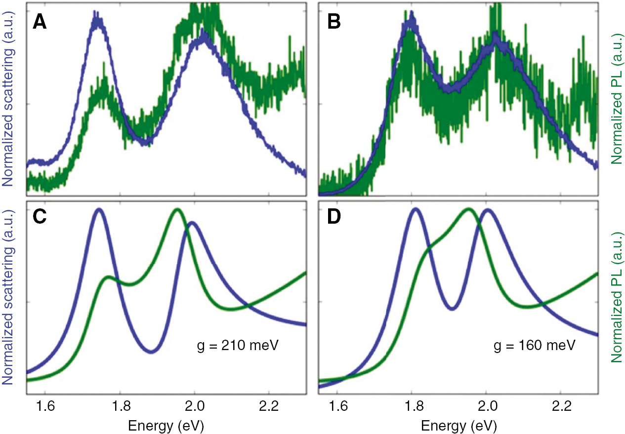
Scattering (blue) and photoluminescence (green) spectra of a single CdSe/CdS QD attached to an AuNP then deposited on a silver film.
Strong coupling is seen through the splitting of both scattering and photoluminescence. Measured spectra are shown for particles deposited directly on the silver film (A) and with a 5 nm silica spacer layer (B–D) show corresponding theoretically calculated spectra.
5 Applications
5.1 Sensors
Extensive work has been done using hybrid plasmonic and semiconductor nanoparticle assemblies as sensors [1], [44], [64]. These systems take advantage of energy transfer from QDs to PNPs, similar to conventional FRET assays. Such systems have been designed to detect the presence of BSA [103], Pb2+, trinitrotoluene [177], avidin [57], proteases, thrombin [99], [178], β-secretase [56], specific oligonucleotides [47], and gene mutations [48]. The concentration-sensitive detection of avidin is shown in Figure 23. PNPs are effective acceptors for FRET-style assays because of their efficient fluorescence quenching due to their large extinction coefficient and broad absorption [1], [57]. Semiconductor QDs make good donors due to their broad absorption and narrow emission spectra with tunable wavelength, photostability, and large quantum yield [1], [56]. As opposed to conventional FRET, which is limited to distances less than 10 nm, PNP-QD based systems have larger effective distances, with detection up to 20 nm [56], [64]. On the contrary, PNPs and QDs are large compared to conventional FRET donor/acceptor molecules and are thus suitable only as assays for sufficiently large molecules.
![Figure 23: Detection of avidin using biotin-AuNPs and streptavidin-QDs.(A) Increase in fluorescence intensity with increasing avidin concentration for a system consisting of streptavidin-functionalized QDs interacting with biotin-functionalized AuNPs. In the absence of avidin, the biotin and streptavidin interact, leading to the quenching of the QD. Avidin addition causes the displacement of the AuNPs and fluorescence is restored. (B) Fluorescence intensity vs. avidin concentration, showing the sensitivity and detection ability of the system. Reprinted with permission from Ref. [57]. Copyright 2005 American Chemical Society.](/document/doi/10.1515/nanoph-2018-0168/asset/graphic/j_nanoph-2018-0168_fig_023.jpg)
Detection of avidin using biotin-AuNPs and streptavidin-QDs.
(A) Increase in fluorescence intensity with increasing avidin concentration for a system consisting of streptavidin-functionalized QDs interacting with biotin-functionalized AuNPs. In the absence of avidin, the biotin and streptavidin interact, leading to the quenching of the QD. Avidin addition causes the displacement of the AuNPs and fluorescence is restored. (B) Fluorescence intensity vs. avidin concentration, showing the sensitivity and detection ability of the system. Reprinted with permission from Ref. [57]. Copyright 2005 American Chemical Society.
Photoelectrochemical sensors based on the transfer of excitons from QDs to PNPs have also been developed [59]. In this case, CdS QDs were tethered to an ITO electrode and functionalized with a target strand of DNA. AgNPs functionalized with complementary DNA stands were then mixed in. Hybridization led to a decrease in the measured photocurrent because excited electrons from the QDs were transferred to the bound AgNPs instead of to the electrode, and AgNPs were bound only if the target DNA was present. This system was sensitive to the presence of the target DNA at subpicomolar levels.
5.2 Light harvesting
Charge transfer between QDs and PNPs also offers the potential for increasing the efficiency of QD-based solar cells by increasing the rate of charge extraction from photoexcited QDs [176], [179]. However, most of the attention on coupled QD-PNP solar cells has focused on the potential for efficiency improvement through enhanced excitation of the QDs [179], [180], [181], [182], [183], [184], [185], [186], [187], [188], [189], [190], [191], [192], [193], [194]. QDs have been extensively investigated for light-harvesting applications, but efficiencies have remained lower than other next-generation solar cells [195]. The addition of PNPs has the potential to increase light absorption in QD solar cells in two ways: (1) through random scattering, which increases the optical path length in the solar cell, and (2) through enhanced excitation of the QDs in the local field of the PNPs [196]. Because optical absorption is a linear process, local field enhancement of absorption in a solar cell with a thick absorbing layer can occur only at the expense of reduced absorption elsewhere in the absorbing layer and cannot improve the total amount of light absorbed. It can, however, increase the absorption in very thin active layers, with thicknesses comparable to the sizes of the PNPs, as the local fields within the active layer can be increased at the expense of the local fields above and below, outside of the active layer. Thin active layers are attractive for QD solar cells, because they will reduce current losses in the disordered, low-mobility QD layers. However, reducing the thickness of the active layer reduced the amount of incident solar radiation that is absorbed, reducing the solar cell efficiency. Coupling PNPs to QDs thus has the potential to improve the power conversion efficiencies (PCEs) of these devices by enhancing absorption in thin active layers. The increase in absorption of one such photovoltaic device with the incorporation of PNPs, and the corresponding increase in PCE, is shown in Figure 24.
![Figure 24: Effect of gold nanoshells on the performance of PbS colloidal QD photovoltaic devices (QD PV).(A) Increase in absorption in a QD PV with incorporation of nanoshells. (B) Difference in absorption of (A) compared to absorption of free nanoshells. (C) Current-voltage characteristics and (D) external quantum efficiency for QD PV with and without plasmonic nanoshells present. Photocurrent efficiency enhancement of 11% was seen. Reprinted with permission from Ref. [191]. Copyright 2013 American Chemical Society.](/document/doi/10.1515/nanoph-2018-0168/asset/graphic/j_nanoph-2018-0168_fig_024.jpg)
Effect of gold nanoshells on the performance of PbS colloidal QD photovoltaic devices (QD PV).
(A) Increase in absorption in a QD PV with incorporation of nanoshells. (B) Difference in absorption of (A) compared to absorption of free nanoshells. (C) Current-voltage characteristics and (D) external quantum efficiency for QD PV with and without plasmonic nanoshells present. Photocurrent efficiency enhancement of 11% was seen. Reprinted with permission from Ref. [191]. Copyright 2013 American Chemical Society.
Particle size [180], [192], shape [183], concentration [179], and separation distance [186] are all known to play a role in the efficiency of plasmon enhanced solar cells. By incorporating PNPs into QD solar cells, increases in PCE ranging from 22% to nearly 100% have been observed, although most have tended toward the lower end of this range [184], [186], [187], [188], [189], [190], [191], [192], [193]. It has been theoretically predicted that using anisotropic PNPs would be the most effective at increasing absorption due to their greater local field enhancement and higher surface area-to-volume ratio, leading to a larger volume of enhancement [181], [182], [183]. This has led researchers to use shapes such as nanostars [185], bipyramids [187], hollow nanoshells [191], and bowtie arrays [194] to increase PCE.
However, a number of challenges face the implementation of PNPs into solar cells. The optimal shapes proposed are complex [182], [183], and synthesizing them remains a challenge. Moreover, the precise positioning of QDs relative to PNPs is needed for these devices to reach the theoretically possible PCE levels; this is likely to increase the fabrication cost of the solar cells, not to mention the increased materials cost associated with AuNPs or AgNPs. In addition, the high absorption of PNPs can reduce the amount of light available to be absorbed by the QDs, and the PNPs can act as charge traps [180]. It has been proposed that absorption by the PNPs could be reduced using aluminum nanoparticles while still maintaining enhanced absorption by the QDs [197], [198]. A more fundamental issue is that using plasmons to increase the absorptivity of QDs also increases the decay rate (i.e. reduces lifetime), leaving less time to extract the excited electrons from the QDs before they recombine [199]. This sets a limit, even in principle, for the maximum photocurrent enhancement that PNPs can provide [200]. All of these limit the usefulness of PNPs for enhanced light harvesting.
5.3 Photocatalysts
Using PNPs to increase the rate at which carriers in QDs are excited by incident light can also increase the rate at which excited electrons are available for catalytic reactions, thereby increasing the photocatalytic activity of the QDs [3], [70], [71], [81], [201], [202]. This has been shown for both the generation of hydrogen gas [3], [81] and the degradation of organic pollutants and dyes [70], [71], [201], leading to up to 10-fold increase in the reaction rate compared to semiconductor QDs without PNPs present [81]. As the increased catalytic activity is based on enhanced excitation, PNP size and PNP-QD separation distance both play a role in the extent of catalytic enhancement observed [3], [70]. For example, it was found that there exists an optimal distance where the enhancement will be largest, and this distance is longer for larger PNPs [3]. At closer distances, nonradiative energy transfer from the photoexcited QD to the surface plasmon dominates and prevents excited electrons from being used to catalyze reactions, similar to the effect that limits the potential of PNPs to enhance the efficiency of solar cells.
6 Future directions
A wide range of applications are theoretically possible by taking advantage of the unique properties that result from the coupling between PNPs and QDs and the formation of hybrid excitations. Because coupling is so sensitive to environmental factors, including temperature, refractive index, and field strength, strongly coupled PNP-QDs have the potential to serve as ultrasensitive, nanoscale sensors [167], [172].
It has been predicted that the coupling strength in PNP-QD systems that exhibit Fano interference depends on the strength of the applied field, leading to a nonlinear Fano effect [147], [149], [154], [157], [158]. A simpler nonlinearity, due to the saturation of the QD, has also been predicted, which has the potential to lead to fully nanoscale systems capable of single-photon modulation [156], [203]. Such a system would have widespread applications in the field of photonics for computing and communication, potentially including quantum information processing [152], [158], [159], [164]. Compared to conventional electronics, it would allow for the high-speed transmission of information with no interference and little loss [150]. Further, it could be used for the creation of nanoscale lasers, antennas, and lenses [204], [205], [206].
Work is still needed into the assembly of such systems and the study of their properties before they become practical in usable devices. However, progress is already under way, and new techniques to obtain a better control of the assembly of PNPs and QDs are continually emerging. Just recently, the first strong coupling of these systems has been demonstrated. Thus, with continued progress, hybrid plasmonic-excitonic nanoparticle assemblies should provide new breakthroughs in the fields of sensing, photonics, and information processing.
References
[1] Yang D, Xu S, Chen Q, Wang Y. One system with two fluorescence resonance energy transfer (FRET) assembles among quantum dots, gold nanoparticles and enzyme. Colloids Surf A Physicochem Eng Aspects 2008;329:38–43.10.1016/j.colsurfa.2008.06.048Suche in Google Scholar
[2] Daniel M-C, Aras O, Smith MF, Nan A, Fleiter T. Targeted in-vivo computed tomography (CT) imaging of tissue ACE using concentrated lisinopril-capped gold nanoparticle solutions. In: Proc. SPIE 7674, Smart Biomedical and Physiological Sensor Technologies VII, 76740J, 2010.10.1117/12.849841Suche in Google Scholar
[3] Torimoto T, Horibe H, Kameyama T, et al. Plasmon-enhanced photocatalytic activity of cadmium sulfide nanoparticle immobilized on silica-coated gold particles. J Phys Chem Lett 2011;2:2057–62.10.1021/jz2009049Suche in Google Scholar
[4] Yuan CT, Yu P, Ko HC, Huang J, Tang J. Antibunching single-photon emission and blinking suppression of CdSe/ZnS quantum dots. ACS Nano 2009;3:3051–6.10.1021/nn900760uSuche in Google Scholar PubMed
[5] Daniel M-C, Astruc D. Gold nanoparticles: assembly, supramolecular chemistry, quantum-size-related properties, and applications toward biology, catalysis, and nanotechnology. Chem Rev 2004;104:293–346.10.1021/cr030698+Suche in Google Scholar PubMed
[6] Alivisatos AP. Semiconductor clusters, nanocrystals, and quantum dots. Science 1996;271:933–7.10.1126/science.271.5251.933Suche in Google Scholar
[7] Lu AH, Salabas EeL, Schüth F. Magnetic nanoparticles: synthesis, protection, functionalization, and application. Angew Chem Int Ed 2007;46:1222–44.10.1002/anie.200602866Suche in Google Scholar PubMed
[8] Dong H, Du S-R, Zheng X-Y, et al. Lanthanide nanoparticles: from design toward bioimaging and therapy. Chem Rev 2015;115:10725–815.10.1021/acs.chemrev.5b00091Suche in Google Scholar PubMed
[9] Turkevich J, Stevenson PC, Hillier J. A study of the nucleation and growth processes in the synthesis of colloidal gold. Disc Faraday Soc 1951;11:55–75.10.1039/df9511100055Suche in Google Scholar
[10] Zabetakis K, Ghann W, Kumar S, Daniel M-C. Effect of high gold salt concentrations on the size and polydispersity of gold nanoparticles prepared by an extended Turkevich-Frens method. Gold Bull 2012;45:203–11.10.1007/s13404-012-0069-2Suche in Google Scholar
[11] Bastús NG, Comenge J, Puntes V. Kinetically controlled seeded growth synthesis of citrate-stabilized gold nanoparticles of up to 200 nm: size focusing versus Ostwald ripening. Langmuir 2011;27:11098.10.1021/la201938uSuche in Google Scholar PubMed
[12] Panácek A, Kvítek L, Prucek R, et al. Silver colloid nanoparticles: synthesis, characterization, and their antibacterial activity. J Phys Chem B 2006;110:16248–53.10.1021/jp063826hSuche in Google Scholar PubMed
[13] Ahmadi TS, Wang ZL, Green TC, Henglein A, El-Sayed MA. Shape-controlled synthesis of colloidal platinum nanoparticles. Science 1996;272:1924.10.1126/science.272.5270.1924Suche in Google Scholar PubMed
[14] Jana NR, Gearheart L, Murphy CJ. Wet chemical synthesis of high aspect ratio cylindrical gold nanorods. J Phys Chem B 2001;105:4065–7.10.1021/jp0107964Suche in Google Scholar
[15] Hao F, Nehl CL, Hafner JH, Nordlander P. Plasmon resonances of a gold nanostar. Nano Lett 2007;7:729–32.10.1021/nl062969cSuche in Google Scholar PubMed
[16] Grzelczak M, Pérez-Juste J, Mulvaney P, Liz-Marzán LM. Shape control in gold nanoparticle synthesis. Chem Soc Rev 2008;37:1783–91.10.1039/b711490gSuche in Google Scholar PubMed
[17] Nath N, Chilkoti A. A colorimetric gold nanoparticle sensor to interrogate biomolecular interactions in real time on a surface. Anal Chem 2001;74:504–9.10.1021/ac015657xSuche in Google Scholar PubMed
[18] Daniel M-C, Grow ME, Pan H, et al. Gold nanoparticle-cored poly (propyleneimine) dendrimers as a new platform for nultifunctional drug delivery systems. N J Chem 2011;35: 2366–74.10.1039/c1nj20206eSuche in Google Scholar
[19] Singh AK, Khan SA, Fan Z, et al. Development of a long-range surface-enhanced Raman spectroscopy ruler. J Am Chem Soc 2012;134:8662–9.10.1021/ja301921kSuche in Google Scholar PubMed
[20] Ratchford D, Shafiei F, Kim S, Gray SK, Li X. Manipulating coupling between a single semiconductor quantum dot and single gold nanoparticle. Nano Lett 2011;11:1049–54.10.1021/nl103906fSuche in Google Scholar PubMed
[21] Fedutik Y, Temnov V, Woggon U, Ustinovich E, Artemyev M. Exciton-plasmon interaction in a composite metal-insulator-semiconductor nanowire system. J Am Chem Soc 2007;129:14939–45.10.1021/ja074705dSuche in Google Scholar PubMed
[22] Naiki H, Masuo S, Machida S, Itaya A. Single-photon emission behavior of isolated CdSe/ZnS quantum dots interacting with the localized surface plasmon resonance of silver nanoparticles. J Phys Chem C 2011;115:23299–304.10.1021/jp207997jSuche in Google Scholar
[23] Munechika K, Chen Y, Tillack AF, et al. Spectral control of plasmonic emission enhancement from quantum dots near single silver nanoprisms. Nano Lett 2010;10:2598–603.10.1021/nl101281aSuche in Google Scholar PubMed
[24] Grzelczak M, Vermant J, Furst EM, Liz-Marzán LM. Directed self-assembly of nanoparticles. ACS Nano 2010;4:3591–605.10.1021/nn100869jSuche in Google Scholar PubMed
[25] Gwo S, Chen H-Y, Lin M-H, Sun L, Li X. Nanomanipulation and controlled self-assembly of metal nanoparticles and nanocrystals for plasmonics. Chem Soc Rev 2016;45:5672–716.10.1039/C6CS00450DSuche in Google Scholar PubMed
[26] Jiang R, Li B, Fang C, Wang J. Metal/semiconductor hybrid nanostructures for plasmon-enhanced applications. Adv Mater 2014;26:5274–309.10.1002/adma.201400203Suche in Google Scholar PubMed
[27] Costi R, Saunders AE, Banin U. Colloidal hybrid nanostructures: a new type of functional materials. Angew Chem Int Ed 2010;49:4878–97.10.1002/anie.200906010Suche in Google Scholar PubMed
[28] Schlather AE, Large N, Urban AS, Nordlander P, Halas NJ. Near-field mediated plexcitonic coupling and giant Rabi splitting in individual metallic dimers. Nano Lett 2013;13:3281–6.10.1021/nl4014887Suche in Google Scholar PubMed
[29] Bellessa J, Symonds C, Vynck K, et al. Giant Rabi splitting between localized mixed plasmon-exciton states in a two-dimensional array of nanosize metallic disks in an organic semiconductor. Phys Rev B 2009;80:033303.10.1103/PhysRevB.80.033303Suche in Google Scholar
[30] Nepal D, Drummy LF, Biswas S, Park K, Vaia RA. Large scale solution assembly of quantum dot-gold nanorod architectures with plasmon enhanced fluorescence. ACS Nano 2013;7:9064–74.10.1021/nn403671qSuche in Google Scholar PubMed
[31] Pons T, Medintz IL, Sapsford KE, et al. On the quenching of semiconductor quantum dot photoluminescence by proximal gold nanoparticles. Nano Lett 2007;7:3157–64.10.1021/nl071729+Suche in Google Scholar PubMed
[32] Sun D, Gang O. Binary heterogeneous superlattices assembled from quantum dots and gold nanoparticles with DNA. J Am Chem Soc 2011;133:5252–4.10.1021/ja111542tSuche in Google Scholar PubMed
[33] Gueroui Z, Libchaber A. Single-molecule measurements of gold-quenched quantum dots. Phys Rev Lett 2004;93:166108.10.1103/PhysRevLett.93.166108Suche in Google Scholar PubMed
[34] Hurst SJ, Lytton-Jean AKR, Mirkin CA. Maximizing DNA loading on a range of gold nanoparticle sizes. Anal Chem 2006;78:8313–8.10.1021/ac0613582Suche in Google Scholar PubMed PubMed Central
[35] Uddayasankar U, Zhang Z, Shergill RT, Gradinaru CC, Krull UJ. Isolation of monovalent quantum dot-nucleic acid conjugates using magnetic beads. Bioconjugate Chem 2014;25:1342–50.10.1021/bc5002032Suche in Google Scholar PubMed
[36] Kolny J, Kornowski A, Weller H. Self-organization of cadmium sulfide and gold nanoparticles by electrostatic interaction. Nano Lett 2002;2:361–4.10.1021/nl0156843Suche in Google Scholar
[37] Wargnier R, Baranov AV, Maslov VG, et al. Energy transfer in aqueous solutions of oppositely charged CdSe/ZnS core/shell quantum dots and in quantum dot-nanogold assemblies. Nano Lett 2004;4:451–7.10.1021/nl0350938Suche in Google Scholar
[38] Cumberland SL, Berrettini MG, Javier A, Strouse GF. Synthesis and characterization of a 1:6 Au-CdSe nanocomposite. Chem Mater 2003;15:1047–56.10.1021/cm010588oSuche in Google Scholar
[39] Strelow C, Theuerholz TS, Schmidtke C, et al. Metal-semiconductor nanoparticle hybrids formed by self-organization: a platform to address exciton-plasmon coupling. Nano Lett 2016;16:4811–8.10.1021/acs.nanolett.6b00982Suche in Google Scholar PubMed
[40] Liu N, Prall BS, Klimov VI. Hybrid gold/silica/nanocrystal-quantum-dot superstructures: synthesis and analysis of semiconductor-metal interactions. J Am Chem Soc 2006;128:15362–3.10.1021/ja0660296Suche in Google Scholar PubMed
[41] Aldeek F, Ji X, Mattoussi H. Quenching of quantum dot emission by fluorescent gold clusters: what it does and does not share with the Förster formalism. J Phys Chem C 2013;117:15429–37.10.1021/jp404952xSuche in Google Scholar
[42] Maneeprakorn W, Malik MA, O’Brien P. Developing chemical strategies for the assembly of nanoparticles into mesoscopic objects. J Am Chem Soc 2010;132:1780–1.10.1021/ja910022qSuche in Google Scholar PubMed
[43] Chang E, Miller JS, Sun J, et al. Protease-activated quantum dot probes. Biochem Biophys Res Commun 2005;334:1317–21.10.1016/j.bbrc.2005.07.028Suche in Google Scholar PubMed
[44] Quach AD, Crivat G, Tarr MA, Rosenzweig Z. Gold nanoparticle-quantum dot-polystyrene microspheres as fluorescence resonance energy transfer probes for bioassays. J Am Chem Soc 2011;133:2028–30.10.1021/ja109348dSuche in Google Scholar PubMed
[45] Li M, Cushing SK, Wang Q, et al. Size-dependent energy transfer between CdSe/ZnS quantum dots and gold nanoparticles. J Phys Chem Lett 2011;2:2125–9.10.1021/jz201002gSuche in Google Scholar
[46] Wang Q, Wang H, Lin C, Sharma J, Zou S, Liu Y. Photonic interaction between quantum dots and gold nanoparticles in discrete nanostructures through DNA directed self-assembly. Chem Commun 2010;46:240–2.10.1039/B915712CSuche in Google Scholar
[47] Uddayasankar U, Krull UJ. Energy transfer assays using quantum dot-gold nanoparticle complexes: optimizing oligonucleotide assay configuration using monovalently conjugated quantum dots. Langmuir 2015;31:8194–204.10.1021/acs.langmuir.5b01932Suche in Google Scholar PubMed
[48] Lee H, Kim A, Kang T, et al. Selective energy transfer between quantum dots and gold nanoparticles for detection of multiple mutations in epidermal growth factor receptor. Anal Lett 2012;45:2707–16.10.1080/00032719.2012.702177Suche in Google Scholar
[49] Yeh H-Y, Yates MV, Mulchandani A, Chen W. Molecular beacon-quantum dot-Au nanoparticle hybrid nanoprobes for visualizing virus replication in living cells. Chem Commun 2010;46:3914–6.10.1039/c001553aSuche in Google Scholar PubMed
[50] Medintz IL, Berti L, Pons T, et al. A reactive peptidic linker for self-assembling hybrid quantum dot-DNA bioconjugates. Nano Lett 2007;7:1741–8.10.1021/nl070782vSuche in Google Scholar PubMed
[51] Zanchet D, Micheel CM, Parak WJ, Gerion D, Williams SC, Alivisatos AP. Electrophoretic and structural studies of DNA-directed Au nanoparticle groupings. J Phys Chem B 2002;106:11758–63.10.1021/jp026144cSuche in Google Scholar
[52] Cohen-Hoshen E, Bryant GW, Pinkas I, Sperling J, Bar-Joseph I. Exciton-plasmon interactions in quantum dot-gold nanoparticle structures. Nano Lett 2012;12:4260–4.10.1021/nl301917dSuche in Google Scholar PubMed
[53] Schreiber R, Do J, Roller E-M, et al. Hierarchical assembly of metal nanoparticles, quantum dots and organic dyes using DNA origami scaffolds. Nat Nano 2014;9:74–8.10.1038/nnano.2013.253Suche in Google Scholar PubMed
[54] Samanta A, Zhou Y, Zou S, Yan H, Liu Y. Fluorescence quenching of quantum dots by gold nanoparticles: a potential long range spectroscopic ruler. Nano Lett 2014;14:5052–7.10.1021/nl501709sSuche in Google Scholar PubMed
[55] Ko SH, Du K, Liddle JA. Quantum-dot fluorescence lifetime engineering with DNA origami constructs. Angew Chem Int Ed 2012;52:1193–7.10.1002/anie.201206253Suche in Google Scholar PubMed
[56] Choi Y, Cho Y, Kim M, Grailhe R, Song R. Fluorogenic quantum dot-gold nanoparticle assembly for beta secretase inhibitor screening in live cell. Anal Chem 2012;84:8595–601.10.1021/ac301574bSuche in Google Scholar PubMed
[57] Oh E, Hong M-Y, Lee D, Nam S-H, Yoon HC, Kim H-S. Inhibition assay of biomolecules based on fluorescence resonance energy transfer (FRET) between quantum dots and gold nanoparticles. J Am Chem Soc 2005;127:3270–1.10.1021/ja0433323Suche in Google Scholar PubMed
[58] Fu Y, Zhang J, Lakowicz JR. Silver-enhanced fluorescence emission of single quantum dot nanocomposites. Chem Commun 2009:313–5.10.1039/B816736BSuche in Google Scholar PubMed PubMed Central
[59] Zhao W-W, Yu P-P, Shan Y, Wang J, Xu J-J, Chen H-Y. Exciton-plasmon interactions between CdS quantum dots and Ag nanoparticles in photoelectrochemical system and its biosensing application. Anal Chem 2012;84:5892–7.10.1021/ac300127sSuche in Google Scholar PubMed
[60] Lee J, Javed T, Skeini T, Govorov AO, Bryant GW, Kotov NA. Bioconjugated Ag nanoparticles and CdTe nanowires: metamaterials with field-enhanced light absorption. Angew Chem Int Ed 2006;45:4819–23.10.1002/anie.200600356Suche in Google Scholar PubMed
[61] Lee J, Govorov A, Dulka J, Kotov NA. Bioconjugates of CdTe nanowires and Au nanoparticles: plasmon-exciton interactions, luminescence enhancement, and collective effects. Nano Lett 2004;4:2323–30.10.1021/nl048669hSuche in Google Scholar
[62] Lee J, Hernandez P, Lee J, Govorov AO, Kotov NA. Exciton-plasmon interactions in molecular spring assemblies of nanowires and wavelength-based protein detection. Nat Mater 2007;6:291–5.10.1038/nmat1869Suche in Google Scholar PubMed
[63] Mandal G, Bardhan M, Ganguly T. Occurrence of Förster resonance energy transfer between quantum dots and gold nanoparticles in the presence of a biomolecule. J Phys Chem C 2011;115:20840–8.10.1021/jp204456kSuche in Google Scholar
[64] Haldar KK, Sen T, Patra A. Metal conjugated semiconductor hybrid nanoparticle-based fluorescence resonance energy transfer. J Phys Chem C 2010;114:4869–74.10.1021/jp911348nSuche in Google Scholar
[65] Focsan M, Gabudean AM, Vulpoi A, Astilean S. Controlling the luminescence of carboxyl-functionalized CdSe/ZnS core-shell quantum dots in solution by binding with gold nanorods. J Phys Chem C 2014;118:25190–9.10.1021/jp501281vSuche in Google Scholar
[66] Slocik JM, Govorov AO, Naik RR. Optical characterization of bio-assembled hybrid nanostructures. Supramol Chem 2006;18:415–21.10.1080/10615800600658925Suche in Google Scholar
[67] Slocik JM, Tam F, Halas NJ, Naik RR. Peptide-assembled optically responsive nanoparticle complexes. Nano Lett 2007;7:1054–8.10.1021/nl070267xSuche in Google Scholar PubMed
[68] Hu T, Isaacoff BP, Bahng JH, et al. Self-organization of plasmonic and excitonic nanoparticles into resonant chiral supraparticle assemblies. Nano Lett 2014;14:6799–810.10.1021/nl502237fSuche in Google Scholar PubMed
[69] Jiang K-Y, Weng Y-L, Guo S-Y, Yu Y, Xiao F-X. Self-assembly of metal/semiconductor heterostructures via ligand engineering: unravelling the synergistic dual roles of metal nanocrystals toward plasmonic photoredox catalysis. Nanoscale 2017;9:16922–36.10.1039/C7NR04802ESuche in Google Scholar PubMed
[70] Rahman DS, Ghosh SK. Manipulating electron transfer in hybrid ZnO-Au nanostructures: size of gold matters. J Phys Chem C 2016;120:14906–17.10.1021/acs.jpcc.6b03551Suche in Google Scholar
[71] Pan Y, Deng S, Polavarapu L, et al. Plasmon-enhanced photocatalytic properties of Cu2O nanowire-Au nanoparticle assemblies. Langmuir 2012;28:12304–10.10.1021/la301813vSuche in Google Scholar PubMed
[72] Kondon M, Kim J, Udawatte N, Lee D. Origin of size-dependent energy transfer from photoexcited CdSe quantum dots to gold nanoparticles. J Phys Chem C 2008;112:6695–9.10.1021/jp800766rSuche in Google Scholar
[73] Orendorff CJ, Hankins PL, Murphy CJ. pH-triggered assembly of gold nanorods. Langmuir 2005;21:2022–6.10.1021/la047595mSuche in Google Scholar PubMed
[74] Jain PK, Eustis S, El-Sayed MA. Plasmon coupling in nanorod assemblies: optical absorption, discrete dipole approximation simulation, and exciton-coupling model. J Phys Chem B 2006;110:18243–53.10.1021/jp063879zSuche in Google Scholar PubMed
[75] Schmidtke C, Kloust H, Bastús NG, et al. A general route towards well-defined magneto- or fluorescent-plasmonic nanohybrids. Nanoscale 2013;5:11783–94.10.1039/c3nr04155gSuche in Google Scholar PubMed
[76] Marcelo G, Burns F, Ribeiro T, et al. Versatile tetrablock copolymer scaffold for hierarchical colloidal nanoparticle assemblies: synthesis, characterization, and molecular dynamics simulation. Langmuir 2017;33:8201–12.10.1021/acs.langmuir.7b01687Suche in Google Scholar PubMed
[77] Ribeiro T, Prazeres TJV, Moffitt M, Farinha JPS. Enhanced photoluminescence from micellar assemblies of cadmium sulfide quantum dots and gold nanoparticles. J Phys Chem C 2013;117:3122–33.10.1021/jp311200rSuche in Google Scholar
[78] Harun NA, Benning MJ, Horrocks BR, Fulton DA. Gold nanoparticle-enhanced luminescence of silicon quantum dots co-encapsulated in polymer nanoparticles. Nanoscale 2013;5:3817–27.10.1039/c3nr00421jSuche in Google Scholar PubMed
[79] Kim B-S, Taton TA. Multicomponent nanoparticles via self-assembly with cross-linked block copolymer surfactants. Langmuir 2007;23:2198–202.10.1021/la062692wSuche in Google Scholar PubMed
[80] Miesch C, Kosif I, Lee E, et al. Nanoparticle-stabilized double emulsions and compressed droplets. Angew Chem Int Ed 2011;51:145–9.10.1002/anie.201106665Suche in Google Scholar PubMed
[81] Shi R, Cao Y, Bao Y, et al. Self-assembled Au/CdSe nanocrystal clusters for plasmon-mediated photocatalytic hydrogen evolution. Adv Mater 2017;29:1700803.10.1002/adma.201700803Suche in Google Scholar PubMed
[82] Lesnyak V, Wolf A, Dubavik A, et al. 3D assembly of semiconductor and metal nanocrystals: hybrid CdTe/Au structures with controlled content. J Am Chem Soc 2011;133:13413–20.10.1021/ja202068sSuche in Google Scholar PubMed
[83] Nahar L, Esteves RJA, Hafiz S, Özgür Ü, Arachchige IU. Metal-semiconductor hybrid aerogels: evolution of optoelectronic properties in a low-dimensional CdSe/Ag nanoparticle assembly. ACS Nano 2015;9:9810–21.10.1021/acsnano.5b02777Suche in Google Scholar PubMed
[84] Shevchenko EV, Talapin DV, Kotov NA, O’Brien S, Murray CB. Structural diversity in binary nanoparticle superlattices. Nature 2006;439:55–9.10.1038/nature04414Suche in Google Scholar PubMed
[85] Shevchenko EV, Talapin DV, Murray CB, O’Brien S. Structural characterization of self-assembled multifunctional binary nanoparticle superlattices. J Am Chem Soc 2006;128:3620–37.10.1021/ja0564261Suche in Google Scholar PubMed
[86] Lu C, Chen Z, O’Brien S. Optimized conditions for the self-organization of CdSe-Au and CdSe-CdSe binary nanoparticle superlattices. Chem Mater 2008;20:3594–600.10.1021/cm703117vSuche in Google Scholar
[87] Shevchenko EV, Ringler M, Schwemer A, et al. Self-assembled binary superlattices of CdSe and Au nanocrystals and their fluorescence properties. J Am Chem Soc 2008;130:3274–5.10.1021/ja710619sSuche in Google Scholar PubMed
[88] Haridas M, Basu JK. Controlled photoluminescence from self-assembled semiconductor-metal quantum dot hybrid array films. Nanotechnology 2010;21:415202.10.1088/0957-4484/21/41/415202Suche in Google Scholar PubMed
[89] Haridas M, Tripathi LN, Basu JK. Photoluminescence enhancement and quenching in metal-semiconductor quantum dot hybrid arrays. Appl Phys Lett 2011;98:063305.10.1063/1.3553766Suche in Google Scholar
[90] Tripathi LN, Haridas M, Basu JK. Exciton plasmon coupling in hybrid semiconductor-metal nanoparticle monolayers. AIP Conf Proc 2009;1147:415–20.10.1063/1.3183467Suche in Google Scholar
[91] Hosoki K, Tayagaki T, Yamamoto S, Matsuda K, Kanemitsu Y. Direct and stepwise energy transfer from excitons to plasmons in close-packed metal and semiconductor nanoparticle monolayer films. Phys Rev Lett 2008;100:207404.10.1103/PhysRevLett.100.207404Suche in Google Scholar PubMed
[92] Sun Z, Wang C, Yang J, Zhao B, Lombardi JR. Nanoparticle metal-semiconductor charge transfer in ZnO/PATP/Ag assemblies by surface-enhanced Raman spectroscopy. J Phys Chem C 2008;112:6093–8.10.1021/jp711240aSuche in Google Scholar
[93] Wu J, Lee S, Reddy VR, Manasreh MO, et al. Photoluminescence plasmonic enhancement in InAs quantum dots coupled to gold nanoparticles. Mater Lett 2011;65:3605–8.10.1016/j.matlet.2011.08.019Suche in Google Scholar
[94] Zayats M, Kharitonov AB, Pogorelova SP, Lioubashevski O, Katz E, Willner I. Probing photoelectrochemical processes in Au-CdS nanoparticle arrays by surface plasmon resonance: application for the detection of acetylcholine esterase inhibitors. J Am Chem Soc 2003;125:16006–14.10.1021/ja0379215Suche in Google Scholar PubMed
[95] Li Y, Chopra N. Gold nanoparticle integrated with nanostructured carbon and quantum dots: synthesis and optical properties. Gold Bull 2015;48:73–83.10.1007/s13404-015-0163-3Suche in Google Scholar
[96] Kulakovich O, Strekal N, Yaroshevich A, et al. Enhanced luminescence of CdSe quantum dots on gold colloids. Nano Lett 2002;2:1449–52.10.1021/nl025819kSuche in Google Scholar
[97] Ozel T, Hernandez-Martinez PL, Mutlugun E, et al. Observation of selective plasmon-exciton coupling in nonradiative energy transfer: donor-selective versus acceptor-selective plexcitons. Nano Lett 2013;13:3065–72.10.1021/nl4009106Suche in Google Scholar PubMed
[98] Komarala VK, Rakovich YP, Bradley AL, et al. Off-resonance surface plasmon enhanced spontaneous emission from CdTe quantum dots. Appl Phys Lett 2006;89:253118.10.1063/1.2422906Suche in Google Scholar
[99] Wang J, Shan Y, Zhao W-W, Xu J-J, Chen H-Y. Gold nanoparticle enhanced electrochemiluminescence of CdS thin films for ultrasensitive thrombin detection. Anal Chem 2011;83:4004–11.10.1021/ac200616gSuche in Google Scholar PubMed
[100] Fedutik Y, Temnov VV, Schöps O, Woggon U, Artemyev MV. Exciton-plasmon-photon conversion in plasmonic nanostructures. Phys Rev Lett 2007;99:136802.10.1103/PhysRevLett.99.136802Suche in Google Scholar PubMed
[101] Dai D, Dong Z, Jiyang F. Giant photoluminescence enhancement in SiC nanocrystals by resonant semiconductor exciton-metal surface plasmon coupling. Nanotechnology 2013;24:025201.10.1088/0957-4484/24/2/025201Suche in Google Scholar PubMed
[102] Kim K-S, Kim J-H, Kim H, et al. Switching off FRET in the hybrid assemblies of diblock copolymer micelles, quantum dots, and dyes by plasmonic nanoparticles. ACS Nano 2012;6:5051–9.10.1021/nn301893eSuche in Google Scholar PubMed
[103] Kurochkina M, Konshina E, Oseev A, Hirsch S. Hybrid structures based on gold nanoparticles and semiconductor quantum dots for biosensor applications. Nanotechnol Sci Appl 2018;11:15–21.10.2147/NSA.S155045Suche in Google Scholar PubMed PubMed Central
[104] Pfeiffer M, Lindfors K, Wolpert C, et al. Enhancing the optical excitation efficiency of a single self-assembled quantum dot with a plasmonic nanoantenna. Nano Lett 2010;10:4555–8.10.1021/nl102548tSuche in Google Scholar PubMed
[105] Graham PM, Gough JJ, Higgins LJ, et al. Ag colloids and arrays for plasmonic non-radiative energy transfer from quantum dots to a quantum well. Nanotechnology 2017;28:115401.10.1088/1361-6528/aa5b67Suche in Google Scholar PubMed
[106] Ma X, Tan H, Kipp T, Mews A. Fluorescence enhancement, blinking suppression, and gray states of individual semiconductor nanocrystals close to gold nanoparticles. Nano Lett 2010;10:4166–74.10.1021/nl102451cSuche in Google Scholar PubMed
[107] Wei H, Ratchford D, Li X, Xu H, Shih C-K. Propagating surface plasmon induced photon emission from quantum dots. Nano Lett 2009;9:4168–71.10.1021/nl9023897Suche in Google Scholar PubMed
[108] Biteen JS, Sweatlock LA, Mertens H, Lewis NS, Polman A, Atwater HA. Plasmon-enhanced photoluminescence of silicon quantum dots: simulation and experiment. J Phys Chem C 2007;111:13372–7.10.1021/jp074160+Suche in Google Scholar
[109] Chan Y-H, Chen J, Wark SE, Skiles SL, Son DH, Batteas JD. Using patterned arrays of metal nanoparticles to probe plasmon enhanced luminescence of CdSe quantum dots. ACS Nano 2009;3:1735–44.10.1021/nn900317nSuche in Google Scholar PubMed
[110] Song J-H, Atay T, Shi S, Urabe H, Nurmikko AV. Large enhancement of fluorescence efficiency from CdSe/ZnS quantum dots induced by resonant coupling to spatially controlled surface plasmons. Nano Lett 2005;5:1557–61.10.1021/nl050813rSuche in Google Scholar PubMed
[111] Viste P, Plain J, Jaffiol R, Vial A, Adam PM, Royer P. Enhancement and quenching regimes in metal-semiconductor hybrid optical nanosources. ACS Nano 2010;4:759–64.10.1021/nn901294dSuche in Google Scholar PubMed
[112] Wang Y, Yang T, Tuominen MT, Achermann M. Radiative rate enhancements in ensembles of hybrid metal-semiconductor nanostructures. Phys Rev Lett 2009;102:163001.10.1103/PhysRevLett.102.163001Suche in Google Scholar PubMed
[113] Gruber C, Trügler A, Hohenau A, Hohenester U, Krenn JR. Spectral modifications and polarization dependent coupling in tailored assemblies of quantum dots and plasmonic nanowires. Nano Lett 2013;13:4257–62.10.1021/nl4019947Suche in Google Scholar PubMed PubMed Central
[114] Najmaei S, Mlayah A, Arbouet A, Girard C, Léotin J, Lou J. Plasmonic pumping of excitonic photoluminescence in hybrid MoS2-Au nanostructures. ACS Nano 2014;8:12682–9.10.1021/nn5056942Suche in Google Scholar PubMed
[115] Mertens H, Biteen JS, Atwater HA, Polman A. Polarization-selective plasmon-enhanced silicon quantum-dot luminescence. Nano Lett 2006;6:2622–5.10.1021/nl061494mSuche in Google Scholar PubMed
[116] Pompa PP, Martiradonna L, Torre AD, et al. Metal-enhanced fluorescence of colloidal nanocrystals with nanoscale control. Nat Nanotechnol 2006;1:126.10.1038/nnano.2006.93Suche in Google Scholar PubMed
[117] Roller E-M, Argyropoulos C, Högele A, Liedl T, Pilo-Pais M. Plasmon-exciton coupling using DNA templates. Nano Lett 2016;16:5962–6.10.1021/acs.nanolett.6b03015Suche in Google Scholar PubMed
[118] Wu Y, Ren S, Xu X, Liu L, Wang H, Yu J. Engineered fluorescence of quantum dots via plasmonic nanostructures. Solar Energy Mater Solar Cells 2014;126:113–9.10.1016/j.solmat.2014.03.050Suche in Google Scholar
[119] Zhang Q, Shan X-Y, Feng X, et al. Modulating resonance modes and Q value of a CdS nanowire cavity by single Ag nanoparticles. Nano Lett 2011;11:4270–4.10.1021/nl2022674Suche in Google Scholar PubMed
[120] Yan Z, Manna U, Qin W, Camire A, Guyot-Sionnest P, Scherer NF. Hierarchical photonic synthesis of hybrid nanoparticle assemblies. J Phys Chem Lett 2013;4:2630–6.10.1021/jz401007tSuche in Google Scholar
[121] Nie K-Y, Tu X, Li J, et al. Tailored emission properties of ZnTe/ZnTe:O/ZnO core-shell nanowires coupled with an Al plasmonic bowtie antenna array. ACS Nano 2018;12:7327–34.10.1021/acsnano.8b03685Suche in Google Scholar PubMed
[122] Tang J, Xia J, Fang M, Bao F, et al. Selective far-field addressing of coupled quantum dots in a plasmonic nanocavity. Nat Commun 2018;9:Article number 1705.10.1038/s41467-018-04077-zSuche in Google Scholar PubMed PubMed Central
[123] Matsuzaki K, Vassant S, Liu H-W, et al. Strong plasmonic enhancement of biexciton emission: controlled coupling of a single quantum dot to a gold nanocone antenna. Sci Rep 2017;7:42307.10.1038/srep42307Suche in Google Scholar PubMed PubMed Central
[124] Groß H, Hamm JM, Tufarelli T, Hess O, Hecht B. Near-field strong coupling of single quantum dots. Sci Adv 2018;4:Article number eaar4906.10.1126/sciadv.aar4906Suche in Google Scholar PubMed PubMed Central
[125] Lee SY, Nakaya K, Hayashi T, Hara M. Quantitative study of the gold-enhanced fluorescence of CdSe/ZnS nanocrystals as a function of distance using an AFM probe. Phys Chem Chem Phys 2009;11:4403–9.10.1039/b819903eSuche in Google Scholar PubMed
[126] Masuo S, Kanetaka K, Sato R, Teranishi T. Direct observation of multiphoton emission enhancement from a single quantum dot using AFM manipulation of a cubic gold nanoparticle. ACS Photonics 2016;3:109–16.10.1021/acsphotonics.5b00496Suche in Google Scholar
[127] Shafran E, Mangum BD, Gerton JM. Using the near-field coupling of a sharp tip to tune fluorescence-emission fluctuations during quantum-dot blinking. Phys Rev Lett 2011;107:037403.10.1103/PhysRevLett.107.037403Suche in Google Scholar PubMed
[128] Farahani JN, Pohl DW, Eisler HJ, Hecht B. Single quantum dot coupled to a scanning optical antenna: a tunable superemitter. Phys Rev Lett 2005;95:017402.10.1103/PhysRevLett.95.017402Suche in Google Scholar PubMed
[129] Masuo S, Tanaka T, Machida S, Itaya A. Photon antibunching in enhanced photoluminescence of a single CdSe/ZnS nanocrystal by silver nanostructures. J Photochem Photobiol A Chem 2012;237:24–30.10.1016/j.jphotochem.2012.04.001Suche in Google Scholar
[130] Ureña EB, Kreuzer MP, Itzhakov S, et al. Excitation enhancement of a quantum dot coupled to a plasmonic antenna. Adv Mater 2012;24:OP314–20.10.1002/adma.201202783Suche in Google Scholar PubMed
[131] Ma X, Fletcher K, Kipp T, et al. Photoluminescence of individual Au/CdSe nanocrystal complexes with variable interparticle distances. J Phys Chem Lett 2011;2:2466–71.10.1021/jz201131uSuche in Google Scholar
[132] Akselrod GM, Weidman MC, Li Y, Argyropoulos C, Tisdale WA, Mikkelsen MH. Efficient nanosecond photoluminescence from infrared PbS quantum dots coupled to plasmonic nanoantennas. ACS Photonics 2016;3:1741–6.10.1021/acsphotonics.6b00357Suche in Google Scholar
[133] Pelton M. Modified spontaneous emission in nanophotonic structures. Nat Photonics 2015;9:427.10.1038/nphoton.2015.103Suche in Google Scholar
[134] Hoang TB, Akselrod GM, Mikkelsen MH. Ultrafast room-temperature single photon emission from quantum dots coupled to plasmonic nanocavities. Nano Lett 2016;16:270–5.10.1021/acs.nanolett.5b03724Suche in Google Scholar PubMed
[135] Govorov AO, Lee J, Kotov NA. Theory of plasmon-enhanced Forster energy transfer in optically excited semiconductor and metal nanoparticles. Phys Rev B 2007;76:125308.10.1103/PhysRevB.76.125308Suche in Google Scholar
[136] Sadeghi SM, West RG. Coherent control of Forster energy transfer in nanoparticle molecules: energy nanogates and plasmonic heat pulses. J Phys Condensed Matter 2011;23:425302.10.1088/0953-8984/23/42/425302Suche in Google Scholar PubMed
[137] Cushing SK, Li J, Meng F, et al. Photocatalytic activity enhanced by plasmonic resonant energy transfer from metal to semiconductor. J Am Chem Soc 2012;134:15033–41.10.1021/ja305603tSuche in Google Scholar PubMed
[138] Govorov AO, Bryant GW, Zhang W, et al. Exciton-plasmon interaction and hybrid excitons in semiconductor-metal nanoparticle assemblies. Nano Lett 2006;6:984–94.10.1021/nl0602140Suche in Google Scholar
[139] Biteen JS, Lewis NS, Atwater HA, Mertens H, Polman A. Spectral tuning of plasmon-enhanced silicon quantum dot luminescence. Appl Phys Lett 2006;88:131109.10.1063/1.2191411Suche in Google Scholar
[140] Nikoobakht B, Burda C, Braun M, Hun M, El-Sayed MA. The quenching of CdSe quantum dots photoluminescence by gold nanoparticles in solution. Photochem Photobiol 2002;75:591–7.10.1562/0031-8655(2002)075<0591:TQOCQD>2.0.CO;2Suche in Google Scholar PubMed
[141] Hoang TB, Akselrod GM, Argyropoulos C, Huang J, Smith DR, Mikkelsen MH. Ultrafast spontaneous emission source using plasmonic nanoantennas. Nat Commun 2015;6:7788.10.1038/ncomms8788Suche in Google Scholar PubMed PubMed Central
[142] Yuan CT, Wang YC, Cheng HW, et al. Modification of fluorescence properties in single colloidal quantum dots by coupling to plasmonic gap modes. J Phys Chem C 2013;117:12762–8.10.1021/jp401993rSuche in Google Scholar
[143] Ackerman PJ, Mundoor H, Smalyukh II, van de Lagemaat J. Plasmon-exciton interactions probed using spatial coentrapment of nanoparticles by topological singularities. ACS Nano 2015;9:12392–400.10.1021/acsnano.5b05715Suche in Google Scholar PubMed
[144] Masuo S, Naiki H, Machida S, Itaya A. Photon statistics in enhanced fluorescence from a single CdSe/ZnS quantum dot in the vicinity of silver nanoparticles. Appl Phys Lett 2009;95:193106.10.1063/1.3259792Suche in Google Scholar
[145] Dey S, Zhao J. Plasmonic effect on exciton and multiexciton emission of single quantum dots. J Phys Chem Lett 2016;7:2921–9.10.1021/acs.jpclett.6b01164Suche in Google Scholar PubMed
[146] Dey S, Zhou Y, Tian X, et al. An experimental and theoretical mechanistic study of biexciton quantum yield enhancement in single quantum dots near gold nanoparticles. Nanoscale 2015;7:6851–8.10.1039/C5NR00274ESuche in Google Scholar PubMed
[147] Park Y-S, Ghosh Y, Chen Y, et al. Super-Poissonian statistics of photon emission from single CdSe-CdS core-shell nanocrystals coupled to metal nanostructures. Phys Rev Lett 2013;110:117401.10.1103/PhysRevLett.110.117401Suche in Google Scholar PubMed
[148] Efros AL, Rosen M. Random telegraph signal in the photoluminescence intensity of a single quantum dot. Phys Rev Lett 1997;78:1110–3.10.1103/PhysRevLett.78.1110Suche in Google Scholar
[149] Zhang W, Govorov AO, Bryant GW. Semiconductor-metal nanoparticle molecules: hybrid excitons and the nonlinear Fano effect. Phys Rev Lett 2006;97:146804.10.1103/PhysRevLett.97.146804Suche in Google Scholar PubMed
[150] Lu Z, Ka-Di Z. Enhancing Kerr nonlinearity of a strongly coupled exciton-plasmon in hybrid nanocrystal molecules. J Phys B Atomic Mol Opt Phys 2008;41:185503.10.1088/0953-4075/41/18/185503Suche in Google Scholar
[151] Yan J-Y, Zhang W, Duan S, Zhao X-G, Govorov AO. Optical properties of coupled metal-semiconductor and metal-molecule nanocrystal complexes: role of multipole effects. Phys Rev B 2008;77:165301.10.1103/PhysRevB.77.165301Suche in Google Scholar
[152] Artuso RD, Bryant GW. Optical response of strongly coupled quantum dot-metal nanoparticle systems: double peaked Fano structure and bistability. Nano Lett 2008;8:2106–11.10.1021/nl800921zSuche in Google Scholar PubMed
[153] Ridolfo A, Di Stefano O, Fina N, Saija R, Savasta S. Quantum plasmonics with quantum dot-metal nanoparticle molecules: influence of the Fano effect on photon statistics. Phys Rev Lett 2010;105:263601.10.1103/PhysRevLett.105.263601Suche in Google Scholar PubMed
[154] Artuso RD, Bryant GW. Strongly coupled quantum dot-metal nanoparticle systems: exciton-induced transparency, discontinuous response, and suppression as driven quantum oscillator effects. Phys Rev B 2010;82:195419.10.1103/PhysRevB.82.195419Suche in Google Scholar
[155] Wu X, Gray SK, Pelton M. Quantum-dot-induced transparency in a nanoscale plasmonic resonator. Opt Express 2010;18:23633–45.10.1364/OE.18.023633Suche in Google Scholar PubMed
[156] Manjavacas A, García de Abajo FJ, Nordlander P. Quantum plexcitonics: strongly interacting plasmons and excitons. Nano Lett 2011;11:2318–23.10.1021/nl200579fSuche in Google Scholar PubMed
[157] Zhang W, Govorov AO. Quantum theory of the nonlinear Fano effect in hybrid metal-semiconductor nanostructures: the case of strong nonlinearity. Phys Rev B 2011;84:081405.10.1103/PhysRevB.84.081405Suche in Google Scholar
[158] Artuso RD, Bryant GW, Garcia-Etxarri A, Aizpurua J. Using local fields to tailor hybrid quantum-dot/metal nanoparticle systems. Phys Rev B 2011;83:235406.10.1103/PhysRevB.83.235406Suche in Google Scholar
[159] Cheng M-T, Song Y-Y. Fano resonance analysis in a pair of semiconductor quantum dots coupling to a metal nanowire. Opt Lett 2012;37:978–80.10.1364/OL.37.000978Suche in Google Scholar PubMed
[160] Hatef A, Sadeghi SM, Singh MR. Plasmonic electromagnetically induced transparency in metallic nanoparticle-quantum dot hybrid systems. Nanotechnology 2012;23:065701.10.1088/0957-4484/23/6/065701Suche in Google Scholar PubMed
[161] Paspalakis E, Evangelou S, Terzis AF. Control of excitonic population inversion in a coupled semiconductor quantum dot metal nanoparticle system. Phys Rev B 2013;87:235302.10.1103/PhysRevB.87.235302Suche in Google Scholar
[162] Sadeghi SM. Gain without inversion in hybrid quantum dot-metallic nanoparticle systems. Nanotechnology 2010;21:455401.10.1088/0957-4484/21/45/455401Suche in Google Scholar PubMed
[163] Kosionic SG, Terzis AF, Sadeghi SM, Paspalakis E. Optical response of a quantum dot-metal nanoparticle hybrid interacting with a weak probe field. J Phys Condensed Matter 2013;25:045304.10.1088/0953-8984/25/4/045304Suche in Google Scholar PubMed
[164] Savasta S, Saija R, Ridolfo A, Di Stefano O, Denti P, Borghese F. Nanopolaritons: vacuum Rabi splitting with a single quantum dot in the center of a dimer nanoantenna. ACS Nano 2010;4:6369–76.10.1021/nn100585hSuche in Google Scholar PubMed
[165] Bryant GW, Artuso RD, Garcia-Etxarri A, Aizpurua J. Using local fields to tailor hybrid quantum dot-metal nanoparticle systems: connecting the dots. In: CLEO: 2011 – Laser Applications to Photonic Applications, OSA Technical Digest (CD) (Baltimore, MD, Optical Society of America, May 1–6, 2011). Paper QThL3.10.1364/QELS.2011.QThL3Suche in Google Scholar
[166] Sadeghi SM, Deng L, Li X, Huang WP. Plasmonic (thermal) electromagnetically induced transparency in metallic nanoparticle-quantum dot hybrid systems. Nanotechnology 2009;20:365401.10.1088/0957-4484/20/36/365401Suche in Google Scholar PubMed
[167] Sadeghi SM. Tunable nanoswitches based on nanoparticle meta-molecules. Nanotechnology 2010;21:355501.10.1088/0957-4484/21/35/355501Suche in Google Scholar PubMed
[168] Li J-B, He M-D, Wang X-J, Peng X-F, Chen L-Q. Switching and Fano resonance via exciton-plasmon interaction. Chin Phys B 2014;23:067302.10.1088/1674-1056/23/6/067302Suche in Google Scholar
[169] Chen W, Chen G-Y, Chen Y-N. Controlling Fano resonance of nanowire surface plasmons. Opt Lett 2011;36:3602–4.10.1364/OL.36.003602Suche in Google Scholar PubMed
[170] Yannopapas V, Paspalakis E, Vitanov NV. Plasmon-induced enhancement of quantum interference near metallic nanostructures. Phys Rev Lett 2009;103:063602.10.1103/PhysRevLett.103.063602Suche in Google Scholar PubMed
[171] Cheng M-T, Liu S-D, Zhou H-J, Hao Z-H, Wang Q-Q. Coherent exciton-plasmon interaction in the hybrid semiconductor quantum dot and metal nanoparticle complex. Opt Lett 2007;32:2125–7.10.1364/OL.32.002125Suche in Google Scholar PubMed
[172] Sadeghi SM. Plasmonic metaresonances: molecular resonances in quantum dot-metallic nanoparticle conjugates. Phys Rev B 2009;79:233309.10.1103/PhysRevB.79.233309Suche in Google Scholar
[173] Hartsfield T, Chang W-S, Yang S-C, et al. Single quantum dot controls a plasmonic cavity’s scattering and anisotropy. Proc Natl Acad Sci 2015;112:12288.10.1073/pnas.1508642112Suche in Google Scholar PubMed PubMed Central
[174] Santhosh K, Bitton O, Chuntonov L, Haran G. Vacuum Rabi splitting in a plasmonic cavity at the single quantum emitter limit. Nat Commun 2016;7:ncomms11823.10.1038/ncomms11823Suche in Google Scholar PubMed PubMed Central
[175] Zhou N, Yuan M, Gao Y, Li D, Yang D. Silver nanoshell plasmonically controlled emission of semiconductor quantum dots in the strong coupling regime. ACS Nano 2016;10:4154–63.10.1021/acsnano.5b07400Suche in Google Scholar PubMed
[176] Leng H, Szychowski B, Daniel M-C, Pelton M. Strong coupling and induced transparency at room temperature with single quantum dots and gap plasmons. Nat Commun [online] 2018;9:Article number 4012.10.1038/s41467-018-06450-4Suche in Google Scholar PubMed PubMed Central
[177] Chen H, Xia Y. Compact hybrid (gold nanodendrite-quantum dots) assembly: plasmon enhanced fluorescence-based platform for small molecule sensing in solution. Anal Chem 2014;86:11062–9.10.1021/ac5031804Suche in Google Scholar PubMed
[178] Rezaei Z, Ranjbar B. Ultra-sensitive, rapid gold nanoparticle-quantum dot plexcitonic self-assembled aptamer-based nanobiosensor for the detection of human cardiac troponin I. Eng Life Sci 2016;17:165–74.10.1002/elsc.201500188Suche in Google Scholar PubMed PubMed Central
[179] Chandra S, Doran J, McCormack SJ, Kennedy M, Chatten AJ. Enhanced quantum dot emission for luminescent solar concentrators using plasmonic interaction. Solar Energy Mater Solar Cells 2012;98:385–90.10.1016/j.solmat.2011.11.030Suche in Google Scholar
[180] Mendes M. J, Luque A, Tobías I, Martí A. Plasmonic light enhancement in the near-field of metallic nanospheroids for application in intermediate band solar cells. Appl Phys Lett 2009;95:071105.10.1063/1.3205470Suche in Google Scholar
[181] Luque A, Martí A, Mendes MJ, Tobías I. Light absorption in the near field around surface plasmon polaritons. J Appl Phys 2008;104:113118.10.1063/1.3014035Suche in Google Scholar
[182] Catchpole KR, Polman A. Design principles for particle plasmon enhanced solar cells. Appl Phys Lett 2008;93:191113.10.1063/1.3021072Suche in Google Scholar
[183] Aubry A, Lei DY, Fernández-Domínguez AI, Sonnefraud Y, Maier SA, Pendry JB. Plasmonic light-harvesting devices over the whole visible spectrum. Nano Lett 2010;10:2574–9.10.1021/nl101235dSuche in Google Scholar PubMed
[184] Kawawaki T, Wang H, Kubo T, et al. Efficiency enhancement of PbS quantum dot/ZnO nanowire bulk-heterojunction solar cells by plasmonic silver nanocubes. ACS Nano 2015;9:4165–72.10.1021/acsnano.5b00321Suche in Google Scholar PubMed
[185] Wu J, Yu P, Susha AS, et al. Broadband efficiency enhancement in quantum dot solar cells coupled with multispiked plasmonic nanostars. Nano Energy 2015;13:827–35.10.1016/j.nanoen.2015.02.012Suche in Google Scholar
[186] Zhao H, Huang F, Hou J, et al. Efficiency enhancement of quantum dot sensitized TiO2/ZnO nanorod arrays solar cells by plasmonic Ag nanoparticles. ACS Appl Mater Interfaces 2016;8:26675–82.10.1021/acsami.6b06386Suche in Google Scholar PubMed
[187] Chen S, Wang Yj, Liu Q, et al. Broadband enhancement of PbS quantum dot solar cells by the synergistic effect of plasmonic gold nanobipyramids and nanospheres. Adv Energy Mater 2017;8:1701194.10.1002/aenm.201701194Suche in Google Scholar
[188] Wang Y, Zhang Q, Huang F, et al. In situ assembly of well-defined Au nanoparticles in TiO2 films for plasmon-enhanced quantum dot sensitized solar cells. Nano Energy 2018;44:135–43.10.1016/j.nanoen.2017.11.078Suche in Google Scholar
[189] Eskandari M, Ahmadi V, Yousefirad M, Kohnehpoushi S. Plasmon enhanced CdS-quantum dot sensitized solar cell using ZnO nanorods array deposited with Ag nanoparticles as photoanode. Phys E Low Dimens Syst Nanostruc 2015;68:202–9.10.1016/j.physe.2014.12.007Suche in Google Scholar
[190] Bhardwaj S, Pal A, Chatterjee K, et al. Enhanced efficiency of PbS quantum dot-sensitized solar cells using plasmonic photoanode. J Nanoparticle Res 2018;20:198.10.1007/s11051-018-4301-8Suche in Google Scholar
[191] Paz-Soldan D, Lee A, Thon SM, et al. Jointly tuned plasmonic-excitonic photovoltaics using nanoshells. Nano Lett 2013;13:1502–8.10.1021/nl304604ySuche in Google Scholar PubMed
[192] Kholmicheva N, Moroz P, Rijal U, et al. Plasmonic nanocrystal solar cells utilizing strongly confined radiation. ACS Nano 2014;8:12549–59.10.1021/nn505375nSuche in Google Scholar PubMed
[193] Wu J, Mangham SC, Reddy VR, Manasreh MO, Weaver BD. Surface plasmon enhanced intermediate band based quantum dots solar cell. Solar Energy Mater Solar Cells 2012;102:44–9.10.1016/j.solmat.2012.03.032Suche in Google Scholar
[194] Nie K-Y, Li J, Chen X, et al. Extreme absorption enhancement in ZnTe:O/ZnO intermediate band core-shell nanowires by interplay of dielectric resonance and plasmonic bowtie nanoantennas. Sci Rep 2017;7:7503.10.1038/s41598-017-07970-7Suche in Google Scholar PubMed PubMed Central
[195] Rauf IA, Rezai P. A review of materials selection for optimized efficiency in quantum dot sensitized solar cells: a simplified approach to reviewing literature data. Renew Sustain Energy Rev 2017;73:408–22.10.1016/j.rser.2017.01.137Suche in Google Scholar
[196] Atwater HA, Polman A. Plasmonics for improved photovoltaic devices. Nat Mater 2010;9:205–13.10.1038/nmat2629Suche in Google Scholar PubMed
[197] Akimov YA, Koh WS. Resonant and nonresonant plasmonic nanoparticle enhancement for thin-film silicon solar cells. Nanotechnology 2010;21:235201.10.1088/0957-4484/21/23/235201Suche in Google Scholar PubMed
[198] Green MA, Pillai S. Harnessing plasmonics for solar cells. Nat Photonics 2012;6:130.10.1038/nphoton.2012.30Suche in Google Scholar
[199] Jin S, DeMarco E, Pellin MJ, Farha OK, Wiederrecht GP, Hupp JT. Distance-engineered plasmon-enhanced light harvesting in CdSe quantum dots. J Phys Chem Lett 2013;4:3527–33.10.1021/jz401801vSuche in Google Scholar
[200] Ramakrishna S, Pelton M, Gray SK, Seideman T. Plasmon-enhanced electron injection in dye-sensitized solar cells. J Phys Chem C 2015;119:22640–5.10.1021/acs.jpcc.5b07660Suche in Google Scholar
[201] Paramasivam I, Macak JM, Schmuki P. Photocatalytic activity of TiO2 nanotube layers loaded with Ag and Au nanoparticles. Electrochem Commun 2008;10:71–5.10.1016/j.elecom.2007.11.001Suche in Google Scholar
[202] Ong WL, Natarajan S, Kloostra B, Ho GW. Metal nanoparticle-loaded hierarchically assembled ZnO nanoflakes for enhanced photocatalytic performance. Nanoscale 2013;5:5568–75.10.1039/c3nr00043eSuche in Google Scholar PubMed
[203] She C, Bryant GW, Demortière A, Shevchenko EV, Pelton M. Controlling the spatial location of photoexcited electrons in semiconductor CdSe/CdS core/shell nanorods. Phys Rev B 2013;87:155427.10.1103/PhysRevB.87.155427Suche in Google Scholar
[204] Antón MA, Carreño F, Melle S, et al. Plasmonic effects in excitonic population transfer in a driven semiconductor metal nanoparticle hybrid system. Phys Rev B 2012;86:155305.10.1103/PhysRevB.86.155305Suche in Google Scholar
[205] Sadeghi SM, Wing WJ, Gutha RR. Undamped ultrafast pulsation of plasmonic fields via coherent exciton-plasmon coupling. Nanotechnology 2015;26:085202.10.1088/0957-4484/26/8/085202Suche in Google Scholar PubMed
[206] Mahi RS. Enhancement of the second-harmonic generation in a quantum dot-metallic nanoparticle hybrid system. Nanotechnology 2013;24:125701.10.1088/0957-4484/24/12/125701Suche in Google Scholar PubMed
©2019 Marie-Christine Daniel et al., published by De Gruyter, Berlin/Boston
This work is licensed under the Creative Commons Attribution-NonCommercial-NoDerivatives 4.0 License.
Artikel in diesem Heft
- Editorial
- Plasmon-exciton coupling
- Special Issue Articles
- Preparation and properties of plasmonic-excitonic nanoparticle assemblies
- High optical magnetism of dodecahedral plasmonic meta-atoms
- Quantum dot plasmonics: from weak to strong coupling
- Enhancing functionalities of atomically thin semiconductors with plasmonic nanostructures
- Six-fold plasmonic enhancement of thermal scavenging via CsPbBr3 anti-Stokes photoluminescence
- Phase-matched nonlinear second-harmonic generation in plasmonic metasurfaces
- Prospects and applications of plasmon-exciton interactions in the near-field regime
- Pliable polaritons: Wannier exciton-plasmon coupling in metal-semiconductor structures
- Polaritonics: from microcavities to sub-wavelength confinement