Interfacing optical fibers with plasmonic nanoconcentrators
-
Alessandro Tuniz

 and
Markus A. Schmidt
and
Markus A. Schmidt

Abstract
The concentration of light to deep-subwavelength dimensions plays a key role in nanophotonics and has the potential to bring major breakthroughs in fields demanding to understand and initiate interaction on nanoscale dimensions, including molecular disease diagnostics, DNA sequencing, single nanoparticle manipulation and characterization, and semiconductor inspection. Although planar metallic nanostructures provide a pathway to nanoconcentration of electromagnetic fields, the delivery/collection of light to/from such plasmonic nanostructures is often inefficient, narrow-band, and requires complicated excitations schemes, limiting widespread applications. Moreover, planar photonic devices reveal a reduced flexibility in terms of bringing the probe light to the sample. An ideal photonic-plasmonic device should combine (i) a high spatial resolution at the nanometre level beyond to what is state-of-the-art in near-field microscopy with (ii) flexible optical fibers to promote a straightforward integration into current near-field scanning microscopes. Here, we review the recent development and main achievements of nanoconcentrators interfacing optical fibers at their end-faces that reach entirely monolithic designs, including campanile probes, gold-coated fiber-taper nanotips, and fiber-integrated gold nanowires.
1 Introduction
Optical fibers are the most widely used light-guiding device, forming the backbone of modern telecommunications and providing an extremely effective tool for broadband light delivery. As a result of their universal presence in both industry and fundamental research, recent years have been marked by an interest in expanding the functionality of optical fibers toward previously inaccessible areas. Two approaches are typically followed. The first involves tailoring the light guidance by modifying the core and cladding either via an appropriate microstructuring or nanostructuring (such as in photonic crystal fibers [1]) or by composited materials (such as in hybrid multimaterial fibers [2], [3], [4]), both of which have led to important developments in multifunctional fiber-based devices, e.g. for nonlinear light generation [5], [6], sensing [7], [8], and optoelectronics [9], to name a few. The second approach involves modifying the end-face or “tip” of an optical fiber – typically formed by a cleaved fiber end-faces – thus using the flexible light guidance to enhance and tailor the interaction of light and analytes of interest surrounding the tip, with one vision being the implementation of a fiber-based “lab-on-a-tip” for remote photonic sensing [10].
Here, we will discuss the second approach, which is of broad interest in nanophotonics, where the efficient delivery and collection of light to the nanoscale is especially significant. Fibers that have sophisticated structures at their tips for nanoconcentration can be used for remote optical sensing [11], biomedicine [12], endoscopy [13], beam shaping [14], filtering [15], and pressure sensing [16] and are particular relevant for near-field microscopy [17] simply by adapting established lithographic techniques to the end-faces of optical fibers. However, many of these fiber-tip devices show a comparable large interaction area limited by diffraction, which for visible light is several hundreds of nanometers. To obtain subdiffraction light confinement, either high-index dielectrics [18] or metals [19] must be incorporated into fiber. High-index dielectrics can increase the resolution simply by reducing the wavelength of propagating light inside the material; metals, on the contrary, allow for nanoscale light confinement through various physical mechanisms. The simplest route to achieving spatial resolution below the diffraction limit is using simple apertures to block out the unwanted light [20], although this produces low throughputs at subwavelength spatial dimensions, because in such regimes the transmitted amplitude scales with b3 (where b is aperture diameter) [21]. A more practical approach involves using metal tips [22], particles [23], or antennas [24], which concentrate electromagnetic fields to the nanoscale and yield a localized intensity enhancement, due to either propagating surface plasmon polaritons (SPPs) or localized surface plasmon resonances (LSPRs) [25], which both rely on collective oscillations of electrons near metal/dielectric interfaces. However, such plasmonic modes are most commonly excited from free space, e.g. via end-fire coupling [26] or via phase matching schemes such as prism [27] or grating [28] coupling; efficiently interfacing such schemes to optical fibers is experimentally challenging. Some examples of plasmonic structures that have been patterned on the core of an optical fiber include metasurfaces [29] forming so-called “fiber meta-tips” [30], and nanoparticle antennas [31], [32], [33], which can enhance light-matter interaction on the remote fiber tip, e.g. for surface-enhanced Raman scattering (SERS) [34], [35] or particle trapping [36]. These devices achieve subdiffraction confinement of light and local intensity enhancement, but due to the different modal overlap between the large fiber mode and the individual nanoscale plasmonic mode, the entire fiber must be covered with nanoparticles to achieve the desired functionality.
The ability to efficiently and controllably confine light down to single-nanometer spatial dimensions has the potential to revolutionize photonic technologies, providing a pathway for monolithic integrated optical nanoscale circuits, single-molecule sensing, particle trapping, and nanoimaging (scanning near-field optical microscopy, SNOM). However, widespread applications have been limited by high losses and low coupling efficiencies. These problems can be addressed using short enough devices and designing optimal couplers, which is in general complicated. Several approaches have targeted high coupling efficiencies to nanoconcentrators, e.g. via gratings [37], annular inscriptions [38], or transmission lines [39]. However, these plasmonic nanoconcentrators are still interrogated from free space. A monolithic and robust fiber-connectorized plasmonic nanoconcentrator directly located on the fiber end-faces would be more practical for most applications, for which various design and technological challenges must first be addressed.
This paper reviews the research progress in the design, fabrication, and characterization of fiber-compatible nanoconcentration techniques to achieve efficient simultaneous confinement and concentration of light to nanoscale dimensions via plasmonic mechanisms, as summarized in the concept schematic of Figure 1. These devices form the current state-of-the art in terms of subwavelength confinement, collection/delivery efficiency, and ease of integration into fully connectorized optical fibers.

Nanoconcentration of light using flexible optical fibers interfacing with plasmonic nanoconcentrators at a fiber tip for the efficient delivery and collection of light to/from deep nanoscale dimensions.
The various plasmonic nanoconcentrators discussed in this review (represented by the four schematics in the figure) include conical nanotips, campanile probes, LSPRs, and BNAs.
1.1 Conventional fiber tips: properties and limitations
One of the first approaches for achieving confinement of light at fiber tips involves using silica fiber tapers with subwavelength diameters [40], which has found widespread applications in photonics, including sensing [11], nonlinear light generation [41], telecommunications [42], imaging [17], and particle trapping [43]. Chemical etching [44], [45] and heating-and-pulling techniques [46] can produce fiber-based deep-subwavelength tips with extremely smooth surfaces. Although silica tapers support a single mode at visible wavelengths down to a waist diameters of ~100 nm (Figure 2A), shrinking them further causes the effective index of the mode to approach unity, indicating leakage of light into free space and preventing subwavelength light concentration below the diffraction limit (Figure 2B). Such “nanospikes” are often used as high-efficiency fiber couplers, e.g. in high-index contrast hybrid fibers for nonlinear applications [47], and also self-align when placed inside large-area hollow-core photonic crystal fibers [48], [49]. This is due to the two to three times enhancement of the intensity in a region close to the fiber tip (~λ/2 spatial confinement), making them suitable for other optomechanical applications such as optical tweezing and particle trapping [43]. For imaging applications, it has been shown that such tips allows spatial resolution in the order of ~70 nm by passing light to the fiber twice [17].
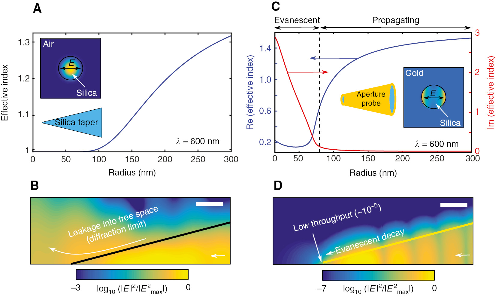
Inherent limits of conventional subwavelength fiber-based nanotips.
(A) Calculated effective index of the fundamental linearly polarized mode a silica nanofiber (inset) as a function of its local radius. For small radii, light leaks into free space (effective index=1) and cannot be confined. (B) Finite element calculations of the intensity (log scale) for a mode propagating toward the apex of a tapered silica nanotip. Black line: edge of the taper. (C) Calculated real (blue) and imaginary (red) parts of the effective index of the fundamental linearly polarized mode a silica nanofiber that is embedded in gold (inset) as a function of its local radius, corresponding to a typical aperture probe. For small radii, the mode cuts off and becomes evanescent, leading to low throughput (1.3×10⁻⁵) through the aperture (diameter: 10 nm). (D) Finite element calculations of the intensity (log scale) of the mode propagating down a tapered aperture probe. Yellow line: edge of the metal-coated taper. Scale bar (B and D), 200 nm. The radius of the fiber at the tip/aperture in B or D is 10 nm. All calculations are performed at λ=600 nm.
One obvious pathway to prevent the leakage of radiation into free space relies on coating the fiber with metal and leaving a nanoaperture at the end-face of the fiber, forming the so-called aperture probe. The diameter of the aperture in fact defines the spatial resolution achievable, so that raster scanning an illuminated sample close to the surface enables imaging with subwavelength resolution. To date, this type of approach is the most widely used method for near-field scanning optical microscopy, owing to its simplicity and ease of integration into most setups, and is readily commercially available (http://www.nanonics.co.il/our-products/nsom-snom-probes). However, one major drawback of this device is its comparably low performance in both collection and delivery operation. This can be understood by considering the properties of the aperture mode as the hole diameter is reduced (Figure 2B): for taper diameters down to ~100 nm, a propagating mode is still supported. However, for smaller diameters, the modes cut off at a significant distance before reaching the end of the fiber and only its evanescent tail reaches the actual aperture at the fiber end, leading to low optical throughput, typically in the order of 10−5 [20]. Although this can be improved by two orders of magnitude by designing the aperture probe such that its mode resonantly couples to the evanescent mode in the tapered region [50] or by placing a monopole antenna close to the aperture [51], better strategies are required to achieve nanoscale spatial confinement accompanied by large-field enhancements and percentage conversion efficiency.
1.2 New strategies for fiber-compatible nanoconcentration
1.2.1 Conical tips
Stockman addressed a fundamental challenge in nano-optics, namely the efficient delivery of optical energy to the nanoscale, orders of magnitude below the diffraction limit in free space [52]. This is achieved via SPPs propagating on a tapered metallic nanowire (i.e. nanocone) with apex size of <10 nm. When travelling toward the apex, the propagating SPPs are adiabatically slowed down and show an increasing localization to the nanotip in all three dimensions, with modal areas of (λ/10)2. Note that although for a cylindrical metal waveguide several modes are supported, only the radially polarized (RP) modes (in terms of the transverse electric field) possess this property of increasing field localization, with all other modes either cutting off or transversely dissipating energy for small lateral tip dimensions [53], [54], similar to tapered dielectric waveguides. RP SPPs are also often referred to as the short-range (SR) surface plasmons and are analogous to the asymmetric plasmonic modes (in terms of the magnetic field) in planar metallic films. They are fundamentally different from long-range (LR) surface plasmons, which are lower-loss symmetric modes. In case of metal films, modal splitting between the SR and LR SPPs emerges for film thicknesses below 100 nm, above which only single-interface plasmon modes exist [54]. In cylindrical wires, this splitting occurs at diameters approximately 10 times larger than the mentioned film thickness, significantly relaxing fabrication and material constrains.
The SR-SPP behavior can be understood in terms of its phase velocity vp=c/neff as a function of wire diameter. Figure 3A shows the phase velocity for a gold wire (εAu=−8.4398+1.4108i [55]) in air (εAir=1), at 600 nm, which asymptotically tends to zero when travelling toward the apex of the nanotip. The subwavelength nature of the plasmonic mode can be regarded as a reduction in the diffraction limit, which is associated with a large effective index of the SPP, Δx ~ λ/2neff, with the spatial confinement being limited only by the size of the tip itself. The corresponding losses are shown in Figure 3A (red) and are between 3 and 20 dB/μm. Although large, they are typically not particularly detrimental due to large intensity enhancements and comparably short sample lengths (Figure 3C), so that large conversion efficiencies to/from the tip can be achieved; for example, Chen et al. [56] reported a 70% collection efficiency at 780 nm for a 6 nm diameter tip using a single emitter embedded in a substrate placed 5 nm from the tip apex.

Fiber-compatible schemes for plasmonic nanoconcentration at the end-faces of optical fibers.
(A) Phase velocity normalized to the speed of light in vacuum (blue) and modal loss (red) of the RP plasmonic mode (inset) for a gold nanowire surrounded by air as a function of local radius. (B) Calculated electric field amplitude of the RP electric mode as a function of the tip radius, showing plasmonic enhancement. (C) Finite element simulations of the intensity for a mode propagating toward the apex of a gold nanocone (apex radius: 2.5 nm). (D) Phase velocity normalized to the speed of light in silica (n=refractive index of silica; blue) and modal loss (red) of the linearly polarized mode supported by a metal-dielectric-metal structure as function of the silica slab width w. The structure consists of a silica slab surrounded two gold nanolayers (gold thickness: 100 nm). (E) Calculated electric field amplitude as a function of the waveguide width w and constant gold thickness through the central slice of the tapered MIM structure (dotted line), showing plasmonic enhancement. (F) Finite element calculations of the spatial distribution of the intensity for a mode propagating down the tapered MIM waveguide in the dotted plane in (E). Scale bar (C and D), 200 nm. All calculations are performed at λ=600 nm.
1.2.2 Metal-insulator-metal (MIM) tips
Another relevant geometry for nanofocusing, which possesses a similar modal behavior – cutoff-free increase modal effective index, decrease in phase velocity, and intensity enhancement – is the so-called metal-insulator-metal (MIM) geometry formed by a central dielectric waveguide surrounded by two metal layers [57]. The effective index and loss as a function of the gap width for 1D layers are shown in Figure 3D. In fiber form, the central dielectric is composed of silica and is coated by gold on two sides. This forms the basis of the so-called “campanile” fiber probe [58], which will be discussed in Section 3. The field enhancement of a typical campanile taper can be as large as a factor of several hundreds (Figure 3E); although less than the conical taper for this particular case, this can be improved by fine tuning the tapered region and the gap width [59]. The 3D finite element simulation of the campanile probe in Figure 3E and F shows that, in contrast to the conical structure, some leakage/reflections occur in the tapered section as for other tapered fiber structures. However, compared to a simple aperture probe, the MIM tapered fiber possesses both tight spatial confinement in case of a 5 nm gap and high delivery efficiency (8% for the structure in Figure 3F as opposed to 0.0013% for the aperture probe in Figure 2D).
2 Coupling to conical plasmonic nanotips
We now review fiber-based geometries that are composed of conical plasmonic tips and support deep-subwavelength nanofocused fields at the tip apex. The discussion of this type of nanoconcentration device addresses two key issues: the first is how to effectively excite the SPP itself on the large side of the taper and the second is how to actually achieve a sharp tip. Fabricating tips is particularly challenging, as it often requires going beyond conventional planar fabrication technologies, given that these geometries are inherently 3D and only partially compatible with planar nanostructuring technology.
2.1 End-fire coupling and mode matching: toward efficient nanowire plasmon excitation
The most common ways to couple fiber and nanocone modes rely on end-fire coupling, adiabatic modal conversion, and phase matching. The most practical and direct way of exciting SPPs, particularly in the context of fiber optics, is via end-fire coupling. However, as a result of the inherently different modal characteristics of SPPs (which can have modal areas of ~100 nm2) and fiber modes (typical modal areas are 10–100 μm2), associated coupling efficiencies are typically low. An example fiber-plasmonic end-fire interface is shown in Figure 4A: a step-index fiber is aligned with the symmetry axis of a silver nanowire. Using typical fiber parameters (silica cladding, 4 μm diameter, doped core Δn=8×10⁻³), the modal overlap [60] between the radially fiber polarized mode (Figure 4B, left) and the SR-SPP of a silver nanowire with 1 μm diameter (Figure 4B, right) is ~17% at λ=633 nm. This results in an overall poor conversion of light from the photonic to the plasmonic mode with most of the energy being lost, as shown in the 3D simulations of Figure 4C. This comparably simple structure is quite challenging to fabricate even using splice-and-pressure-assisted melt filling of gold, whereas the issues of core/nanocone alignment and air gaps at the splice point introduce additional losses and scattering at the fiber/nanowire junction.
![Figure 4: Schematics of typical structures that use end-fire coupling to excite the plasmonic modes.(A) State-of-the-art few-mode fiber (core radius: 2 μm, index difference: 8×10⁻³) that interfaces a plasmonic nanowire (radius: 1 μm). (B) Calculated mode profiles for the RP modes of fiber (left) and SPP (right). (C) Propagation simulations, showing that the incoming field is partially reflected and scattered, with only a small portion being coupled to the nanowire mode. (D) Schematic of the geometry proposed in Ref. [56], which showed improving end-fire coupling. Here, a thin silica dielectric fiber (radius: 342 nm) located in air interfaces with a gold nanowire (radius: 164 nm). (E) Calculated mode profiles for the corresponding RP modes of fiber (left) and SPP (right). (F) Propagation simulations showing that most of the light is coupled to the plasmon mode (up to 99% [56]).](/document/doi/10.1515/nanoph-2018-0015/asset/graphic/j_nanoph-2018-0015_fig_004.jpg)
Schematics of typical structures that use end-fire coupling to excite the plasmonic modes.
(A) State-of-the-art few-mode fiber (core radius: 2 μm, index difference: 8×10⁻³) that interfaces a plasmonic nanowire (radius: 1 μm). (B) Calculated mode profiles for the RP modes of fiber (left) and SPP (right). (C) Propagation simulations, showing that the incoming field is partially reflected and scattered, with only a small portion being coupled to the nanowire mode. (D) Schematic of the geometry proposed in Ref. [56], which showed improving end-fire coupling. Here, a thin silica dielectric fiber (radius: 342 nm) located in air interfaces with a gold nanowire (radius: 164 nm). (E) Calculated mode profiles for the corresponding RP modes of fiber (left) and SPP (right). (F) Propagation simulations showing that most of the light is coupled to the plasmon mode (up to 99% [56]).
Chen et al. [56] showed in simulations that this can be significantly improved using a silica nanofiber in air that interfaces a silver nanowire (schematic in Figure 4D). Here, simple modal overlap integration between the dielectric mode (Figure 4E, left) and the SPP mode (Figure 4E, right) is not sufficient to predict the coupling efficiency, as a result of the nontrivial modal interaction at the boundary. Indeed, finite element simulations show almost 100% conversion efficiency from the fiber mode to the SPP (Figure 4F). It was also found that “rounding the edges” of the nanowire at the silica/gold boundary improved the coupling efficiency significantly. This kind of interface thus provides the first pathway to efficiently couple light to nanoscale dimensions and vice versa; it was also predicted that the tapered silver nanowire potentially allows to collect 70% of the light from a point source placed 5 nm below the nanowire. Note, however, that fabricating this particular structure is extremely challenging in terms of obtaining large aspect ratio tapers and precisely producing the required dielectric fiber and nanowire diameters with nanometer precision (including rounded edges). Also placing the nanowire at the center of the dielectric cylinder with such small diameter is crucial, as small deviations from the optimal position would reduce the coupling efficiency significantly.
2.2 Adiabatic modal conversion of SPPs on metal-coated fiber tapers
Metal-coated fibers shaped into a cone terminating into a sharp apex can also be used to convert the RP mode propagating “inside” the fiber taper to the RP plasmons on the “outer” film that are superfocused at the sharp apex (Figure 5A, inset). This was shown theoretically by several groups [62], [63], [64], [65] and later demonstrated experimentally [61], [66]. In essence, it relies on adiabatically transferring the RP dielectric mode into the plasmonic mode. Figure 5A shows the effective indices of the RP modes for a metal-coated tapered fiber. As the radius of a silica nanofiber decreases, the effective index asymptotically would tend to unity (Figure 2A). In this case, however, the dielectric-like mode anticrosses with the (external) SR-SPP mode, which has the same properties as an SR-SPP of a solid gold wire (green dashed line). The two modes couple strongly and split at the anticrossing point, so that the dielectric mode (Figure 5B) transitions into the external SPP mode (Figure 5C). Thus, the “internal” RP fiber mode (Figure 5B) transitions to a guided “external” SPP (Figure 5C) outside the metal film (metal/air interface; Figure 5A, red line; Figure 5D shows full 3D FE simulations of this transition). This coupling process can also be interpreted as a nanofiber equivalent of the planar Kretschmann configuration [27], where phase matching has been achieved between the radial SPP and the fiber core mode [61].
![Figure 5: Superfocusing of SPPs on a metal-coated optical fiber tip.(A) Real part of the effective index for the relevant modes supported in a typical experimental configuration [61]. The red curve represents the RP dielectric (internal) mode (intensity distribution at R=1 μm shown in B) of the fiber that anticrosses with the (external) RP plasmonic mode (shown in C at R=0.3 μm; dashed green line), enabling plasmonic adiabatic tapering. (D) 3D finite element simulation illustrating the evolution of the intensity (|Ez|2) of the mode that incidence from the right into the fiber tip. Inset: field enhancement at the plasmonic tip due to the axially polarized mode. (E) Example of a gold-coated fiber tip (gold thickness: 30 nm, plasmonic tip radius: 100 nm) excited by an RP mode (λ=780 nm). Top: SEM image of the fiber structure. Also shown are polarization resolved optical microscope images of the light emitted from the tip. Middle/bottom: horizontally/vertical oriented polarizer between tip and camera (adapted from Ref. [61]). Reprinted with permission from Ref. [61]. Copyright 2015 American Chemical Society.](/document/doi/10.1515/nanoph-2018-0015/asset/graphic/j_nanoph-2018-0015_fig_005.jpg)
Superfocusing of SPPs on a metal-coated optical fiber tip.
(A) Real part of the effective index for the relevant modes supported in a typical experimental configuration [61]. The red curve represents the RP dielectric (internal) mode (intensity distribution at R=1 μm shown in B) of the fiber that anticrosses with the (external) RP plasmonic mode (shown in C at R=0.3 μm; dashed green line), enabling plasmonic adiabatic tapering. (D) 3D finite element simulation illustrating the evolution of the intensity (|Ez|2) of the mode that incidence from the right into the fiber tip. Inset: field enhancement at the plasmonic tip due to the axially polarized mode. (E) Example of a gold-coated fiber tip (gold thickness: 30 nm, plasmonic tip radius: 100 nm) excited by an RP mode (λ=780 nm). Top: SEM image of the fiber structure. Also shown are polarization resolved optical microscope images of the light emitted from the tip. Middle/bottom: horizontally/vertical oriented polarizer between tip and camera (adapted from Ref. [61]). Reprinted with permission from Ref. [61]. Copyright 2015 American Chemical Society.
Energy transfer is expected to be more efficient in the infrared with a reduced confinement and slightly less efficient in the visible but with tighter localization [65]. The full coupling process subtly depends on shape of the tip, taper angle, modal transition length, and metal film thickness: up to 40% tip transmission can be reached in the visible. These results warrant a comprehensive study of the tradeoff between the long taper lengths and by the adiabatic condition [67] and the short taper lengths required to reduce plasmonic losses to acceptable levels.
Figure 5E (top) shows a typical tapered fiber tip coated by gold. In delivery mode, it was shown that light coupled into the fiber is localized at the tip and polarized along the fiber axis, confirming the excitation of the SPP mode (Figure 5E, middle: polarizer between sample and camera is along the fiber axis; bottom: polarizer between sample and camera is perpendicular the fiber axis). In collection mode, the light polarized along the taper tip axis was collected and converted into an RP mode in the fiber, which was applied to detecting the transversal fields of scattered modes.
This scheme is flexible in terms of design and highly compatible with fiber technology; however, tips with radii smaller than ~125 nm are difficult to achieve as a result of the granular nature of gold, a limitation that should be addressed for it to be competitive with commercial systems in terms of resolution. Finally, it should be noted that, for efficient operation in delivery mode, an isolated TM01 is required in the fiber; this being a higher-order mode, long lengths of fiber result in random mode scrambling to other modes that do not excite the SR-SPP, resulting in a decrease in performance.
2.3 Gold-filled nanobore optical fiber
The issue of precisely aligning metal nanowires with the core of a dielectric fiber (see Figure 4) can be addressed using pressure-assisted melt filling (PAMF) [68]. With this technique, it is possible to interface metal nanowires (e.g. gold) with diameters of a few hundred nanometers and lengths of several centimeters within a glass capillary or fiber containing one or more nanochannels in its core and/or cladding. The ductility of gold enables the immediate generation of nanotips at fiber end-faces, which possess an apex size of ~10 nm, via a straightforward fiber cleave [69]. In this approach, the tip is formed naturally and uses a quasi-bottom-up strategy, which does not require complex top-down nanofabrication technologies, which struggle to reach dimensions of 10 nm or below.
This technique was recently applied to an microstructured optical fiber including a central gold filled nanochannel (or nanobore) [70], [71], leading to a perfect and monolithic alignment between fiber core and gold nanowire. Based on this geometry, it was recently proposed and experimentally verified that a fully integrated fiber-based near-field nanoprobe can deliver light to nanoscale dimensions (apex size of <10 nm) even after propagating hundreds of micrometers. Such lengths are normally prohibitive for SR-SPP propagation as a result of losses. However, using the dielectric-like hybrid mode, it is possible to couple to the SR-SPP, albeit with a lower efficiency, using the so-called “hybrid mode-assisted” SPP excitation scheme. The device is shown in Figure 6A: a cylindrical silica step-index fiber that incorporates a central nanochannel is partially filled with gold and cleaved at an appropriate location to produce a nanotip, on which the light is propagating and focused. Figure 6A (inset) shows an example tip apex (<10 nm). The device functions by exciting the two RP modes in the gold-filled section – the first being dielectric (most of the energy in the dielectric) and the other plasmonic (most energy near the gold surface). As the plasmonic-type mode fully decays after a few micrometers, only the dielectric-like mode “survives” and via its tails in the metal excites the SR plasmonic mode at the fiber end-face, which then gets focused on the tip. The hybrid nature of the dielectric mode thus relaxes the fabrication constrains, allowing functional devices with nanowire lengths between tens and hundreds of micrometers. However, as only a small portion of the energy is near the gold surface for this mode, the conversion efficiency is in the order of 0.1% [70].
![Figure 6: Nanobore fiber-based near-field probe consisting of a gold nanowire inside the fiber core with protruding gold nanotip.(A) Schematic of the monolithic near-field nanoprobe excited by either RP or AP mode. The magenta dot at the front of the tip indicates the intensity enhancement. The inset shows an SEM of a typical gold nanotip, with the sub-10 nm tip region highlighted in green. (B) Illustration of the operating principle: the input core mode (dark green) excites two hybrid EMs (dual-mode region) that propagate in the gold-filled region. The SR-SPP mode has high loss and rapidly decays, so that the TM01 is the dominant mode at the fiber end-face. The RP field on the gold surface is focused at the apex via the SR-SPP travelling down the tip; the field in the dielectric core diffracts into free space. (C) Microscopic image of side scattered light for an RP input state for a short (left) and long (right) nanowire inside the fiber. Highlighted are the empty (blue) and nanowire (orange) regions. The scattered light originating from the nanotip is indicated by magenta arrows. (D) Detailed view of the measured scattered light when the input is RP (top) or AP (bottom). (E) Also shown is the scattered light with a polarizer inserted between sample and camera that is either axially (top) or transversely oriented (bottom). The orientation of the polarizer with respect to the nanotip axis is indicated by white double-headed arrows. All data are for λ=650 nm. Adapted from Ref. [69]. Reprinted with permission from Ref. [70]. Copyright 2017 American Chemical Society.](/document/doi/10.1515/nanoph-2018-0015/asset/graphic/j_nanoph-2018-0015_fig_006.jpg)
Nanobore fiber-based near-field probe consisting of a gold nanowire inside the fiber core with protruding gold nanotip.
(A) Schematic of the monolithic near-field nanoprobe excited by either RP or AP mode. The magenta dot at the front of the tip indicates the intensity enhancement. The inset shows an SEM of a typical gold nanotip, with the sub-10 nm tip region highlighted in green. (B) Illustration of the operating principle: the input core mode (dark green) excites two hybrid EMs (dual-mode region) that propagate in the gold-filled region. The SR-SPP mode has high loss and rapidly decays, so that the TM01 is the dominant mode at the fiber end-face. The RP field on the gold surface is focused at the apex via the SR-SPP travelling down the tip; the field in the dielectric core diffracts into free space. (C) Microscopic image of side scattered light for an RP input state for a short (left) and long (right) nanowire inside the fiber. Highlighted are the empty (blue) and nanowire (orange) regions. The scattered light originating from the nanotip is indicated by magenta arrows. (D) Detailed view of the measured scattered light when the input is RP (top) or AP (bottom). (E) Also shown is the scattered light with a polarizer inserted between sample and camera that is either axially (top) or transversely oriented (bottom). The orientation of the polarizer with respect to the nanotip axis is indicated by white double-headed arrows. All data are for λ=650 nm. Adapted from Ref. [69]. Reprinted with permission from Ref. [70]. Copyright 2017 American Chemical Society.
For an RP input, the side-scattered light showed a bright spot at the fiber end-face, which is unaffected by the length of the nanowire (Figure 6C), in support of the hybrid mode-assisted excitation scheme. Additionally, the fiber scatters the most when the input is RP (Figure 6D) and the least when it is azimuthally polarized (AP), in agreement with expectations. Finally, it was shown that the light at the apex is axially polarized (Figure 6E), as expected for SPP focusing. This indicates that the scattered light originates from the SPP mode and reaches nanotips with apex dimensions below 10 nm.
The hybrid mode-assisted technique, although practical in terms of fabrication and monolithicity, is limited in coupling efficiency due to the large mode mismatch between dielectric and plasmonic modes as a result of the small dimensions of the nanowire compared to the fiber core. Additionally, end-fire coupling does not allow for the selective excitation of a desired mode and requires the appropriate input polarization state to be prepared. As we now show, this issue can be overcome in a directional coupling scheme.
2.4 Optical fiber with wire satellite next to the core
An alternate technique for the efficient excitation of SPPs is plasmonic directional coupling, which requires phase matching between neighboring waveguides. Inspired by previous planar plasmonic directional coupling designs [72], [73], it was suggested to design a hybrid fiber plasmonic focusing device that is compatible with standard optical fibers and can be fabricated using PAMF [74] (Figure 7A). The hybrid device is formed by two parallel running waveguides, whose modes have the same effective index when their separation is infinitely large (phase-matching condition); when the waveguides are brought together, their separation determines the strength of the hybridization (i.e. the difference between the two supermode effective indices Δneff) and thus the plasmonic coupling length Lc, which equals half the beat length of the two eigenmodes (EMs), Lc=λ/2Δneff. The modal evolution along the coupler is well described by an EM analysis, whereby the total electric and magnetic fields in the dual mode region (Figure 7A) are expressed as a superposition of the two supported hybrid EMs. This EM analysis confirmed that the excitation of the plasmon mode is typically quite efficient (in the order of 40%) and broadband (λ=1.4–2 μm) over a short coupling length of only a few micrometers.
![Figure 7: Simulated characteristics of the fiber-based hybrid plasmonic directional coupler.(A) 2D scheme of the couplers including all relevant modes. The dielectric core mode excites two hybrid EMs in the dual waveguide region, which propagate and beat to excite an SR-SPP after a defined propagation length at the end of the device that is nanofocused using the tip. (B) Real part of the effective indices of the hybrid modes of a fiber-based plasmonic directional mode coupler for the excitation of the RP plasmonic mode on the nanowire (core diameter: 1 μm, wire diameter: 0.5 μm, edge-to-edge separation: 0.5 μm, light blue: core index=1.67, dark blue: silica cladding, yellow: gold satellite). (C) SEM image of a two-hole capillary to be filled with a high-index dielectric (core) and gold (wire). Scale bar, 1 μm. (D–G). Spatial distributions of the Poynting vector of the hybrid plasmonic directional coupler that includes a nanotip at characteristic spatial positions (λ=1.55 μm) [74]. (D) Distribution around the coupling region (central xz-plane) calculated using approach discussed in Ref. [74]. The dashed line indicates the coupling length. Finite element simulations at the end of the fiber (E) and at the end of the apex (F: xz-plane and G: xy-plane; both 1 nm away from the apex). Adapted with permission from Ref. [74].](/document/doi/10.1515/nanoph-2018-0015/asset/graphic/j_nanoph-2018-0015_fig_007.jpg)
Simulated characteristics of the fiber-based hybrid plasmonic directional coupler.
(A) 2D scheme of the couplers including all relevant modes. The dielectric core mode excites two hybrid EMs in the dual waveguide region, which propagate and beat to excite an SR-SPP after a defined propagation length at the end of the device that is nanofocused using the tip. (B) Real part of the effective indices of the hybrid modes of a fiber-based plasmonic directional mode coupler for the excitation of the RP plasmonic mode on the nanowire (core diameter: 1 μm, wire diameter: 0.5 μm, edge-to-edge separation: 0.5 μm, light blue: core index=1.67, dark blue: silica cladding, yellow: gold satellite). (C) SEM image of a two-hole capillary to be filled with a high-index dielectric (core) and gold (wire). Scale bar, 1 μm. (D–G). Spatial distributions of the Poynting vector of the hybrid plasmonic directional coupler that includes a nanotip at characteristic spatial positions (λ=1.55 μm) [74]. (D) Distribution around the coupling region (central xz-plane) calculated using approach discussed in Ref. [74]. The dashed line indicates the coupling length. Finite element simulations at the end of the fiber (E) and at the end of the apex (F: xz-plane and G: xy-plane; both 1 nm away from the apex). Adapted with permission from Ref. [74].
The example of interest is a realistic equivalent fiber-like superfocusing device consisting of two parallel cylindrical wires (one dielectric and one gold) embedded in silica, where the gold nanotip forms naturally during the fiber cleave. To provide a sense of the geometric parameters required, at λ=1.55 μm, the SR-SPP mode of a 500-nm-diameter gold nanowire phase matches with the fundamental core mode of a step-index fiber waveguide of 1 μm diameter and refractive index ncore=1.67, which is compatible with current fabrication techniques of hybrid optical fibers [2]. As an example, Figure 7C shows a two-hole capillary to be selectively filled with a high-index dielectric material and gold. Mode evolution simulations (Figure 7D) predict a remarkable power transfer of ~53% after a coupling length of Lc=22 μm. By cleaving at this location to form a conical tip – so that the first part of the wire is embedded in silica and the second part tapers in down a nanoapex in air – such a mode then undergoes plasmonic concentration (5 nm tip radius) over a length of 0.5 μm (Figure 7E–G) with spot sizes of ~10 nm (Figure 7E and F).
3 Coupling to MIM: the campanile structure
An alternative fiber-based near-field plasmonic probe design based on the MIM gap structure [57] was recently proposed and experimentally verified [58]. This tip was termed the “campanile” probe due to its bell tower-like profile and relies on the increasing effective index of the fundamental (symmetric) linearly polarized surface plasmon mode of the MIM as the dielectric gap decreases (Figure 3D–F). As with conical metallic nanotips, the subwavelength plasmonic mode is adiabatically compressed to sub-10 nm dimensions over an extremely large spectral bandwidth (reported wavelengths range between 500 and 1000 nm [58] and can also reach near-infrared [59]). One notable difference compared to the conical tip is that the input is linearly and not RP, considerably simplifying the input mode conditions. Recent progress has shown that this structure can even be 3D printed onto fibers using nanoimprint lithography [75], with 70 nm feature sizes, promising an industrially scalable pathway for low-cost mass production of near-field tips that can be easily integrated into existing commercial systems.
The first fiber-integrated campanile probe was reported in 2012 [58] and is shown in Figure 8A. A tapered silica fiber end-face (~3 μm diameter, corresponding to a commercially available optical fiber with an exposed core at its tip) possesses a protruding campanile (~1 μm base) and terminates with a pyramid that is enclosed on two sides by gold nanolayers. The combination of etching, focused ion beam (FIB) milling, and thin-film technology allows for the production of nanoscale gap sizes down to a few tens of nanometers (in this case, ~40 nm as shown in Figure 8A, inset). Note that although the gold layers are only present on two of four sides of the campanile, the electromagnetic energy is compressed in all three dimensions.
![Figure 8: Campanile nanoconcentrator at the end of an optical fiber.(A) Campanile geometry that is composed of a tapered MIM waveguide fabricated at the end of a tapered glass fiber by FIB milling. From Ref. [58]. Reprinted with permission from AAAS. (B) More recent fabrication approach that uses nanoimprint lithography for mass production. Adapted from Ref. [75] under a Creative Commons CC BY. (C) Demonstration of nano-optical hyperspectral mapping of an InP nanowire using the campanile device (SEM image shown in the top image), showing that the campanile system provides much higher spatial resolution (middle plot) than it can achieved using confocal microscopy (bottom plot). From Ref. [58]. Reprinted with permission from AAAS.](/document/doi/10.1515/nanoph-2018-0015/asset/graphic/j_nanoph-2018-0015_fig_008.jpg)
Campanile nanoconcentrator at the end of an optical fiber.
(A) Campanile geometry that is composed of a tapered MIM waveguide fabricated at the end of a tapered glass fiber by FIB milling. From Ref. [58]. Reprinted with permission from AAAS. (B) More recent fabrication approach that uses nanoimprint lithography for mass production. Adapted from Ref. [75] under a Creative Commons CC BY. (C) Demonstration of nano-optical hyperspectral mapping of an InP nanowire using the campanile device (SEM image shown in the top image), showing that the campanile system provides much higher spatial resolution (middle plot) than it can achieved using confocal microscopy (bottom plot). From Ref. [58]. Reprinted with permission from AAAS.
A comprehensive numerical study [59] showed that the field enhancements of an apertureless tip and the campanile geometry are comparable when both possess 2 nm feature sizes at the apex, with the apertureless tip providing one order of magnitude larger enhancement for 10 nm feature sizes. In collection mode, the energy reaching the optical fiber is between 10% and 60% in the range of 650–1000 nm and drops off for shorter wavelengths. It was recently shown that this enhancement can be significantly improved by a diffractive optical element placed between the fiber and the campanile probe [76], which can also potentially be 3D printed.
The high performance of this device as a practical fiber-connected near-field probe was used to map radiative recombination of InP nanowires [59], which crucially require both near-field excitation and collection over a broad band. The results are shown in Figure 8D: the scanning electron microscopy (SEM) image (top) reveals a 95 nm width, which is imaged using the campanile probe (middle), with significant loss in resolution when using a confocal microscope (bottom). Furthermore, the deep-subwavelength spectral characteristics of the nanowires (not shown) could be mapped, which was not possible using a confocal microscope due to a lack in resolution.
4 Other strategies
4.1 Fiber-based photonic-plasmonic circuits
Another avenue for coupling fiber modes to SPPs was demonstrated by Li et al., who integrated a silver nanowire directly onto the end-face of a tapered optical fiber [77]. They adapted existing techniques [78] for coupling to plasmonic nanowires and nanocircuits via optical fibers, which relied on the nanowire resting on a substrate, to produce nanowires that are monolithically attached to the fiber in free space. The individual silver nanowires were fabricated by chemically reducing silver nitrate with ethylene glycol and polyvinyl pyrrolidone using a self-seeding process [79]. This produces nanowires of nominally 200 nm diameter and several tens of micrometers in length. The fiber tapers were made with a regular standard flame-heated technique down to a 300 nm waist. When a silver nanowire was brought in contact with the tapered fiber using tip micromanipulation, it remained attached to fiber due to van der Waal forces, possessing sufficient mechanical strength for many applications. Figure 9A shows a typical SEM of the resulting hybrid fiber plasmonic device.
![Figure 9: Silver nanowire integrated onto the end-face of a tapered optical.(A) SEM image of the fabricated structure [77]. (B) Microscope side image in the situation light at a wavelength of 785 nm is coupled into the device. (C) 3D finite element simulations showing the Poynting vector magnitude distribution in the vicinity of the nanowire. Here, a linearly polarized input mode is capable of exciting an LR plasmonic mode on the nanowire. The color bar is clipped to 25% of the maximum value. (A and B) Adapted with permission from Ref. [77].](/document/doi/10.1515/nanoph-2018-0015/asset/graphic/j_nanoph-2018-0015_fig_009.jpg)
Silver nanowire integrated onto the end-face of a tapered optical.
(A) SEM image of the fabricated structure [77]. (B) Microscope side image in the situation light at a wavelength of 785 nm is coupled into the device. (C) 3D finite element simulations showing the Poynting vector magnitude distribution in the vicinity of the nanowire. Here, a linearly polarized input mode is capable of exciting an LR plasmonic mode on the nanowire. The color bar is clipped to 25% of the maximum value. (A and B) Adapted with permission from Ref. [77].
Figure 9B shows experimental side images of the light scattered by the silver nanowire (right) when light (λ=785 nm) is coupled into the fiber (left) with fiber/plasmon coupling efficiency and propagation losses of 92% and 0.41 dB/μm (corresponding to the expected loss of LR plasmons for such nanowire thickness and wavelength). The high efficiency of the coupling mechanism can be understood as follows: as the linearly polarized mode of the optical fiber taper cuts off (Figure 2), the light can efficiently couple into the linearly polarized LR plasmon of the attached silver nanowire, establishing a nearly adiabatic transition from the dielectric optical fiber mode into the plasmonic mode of the silver nanowire.
Although the authors suggest that this might be useful for near-field imaging, optical sensing, and nanoscale endoscopy, the achievable confinement is not better than the diffraction limit, due to the excitation of the linearly polarized SPP mode, possessing an effective index that approaches unity in air. As a result, the nanoconcentration that can be achieved is limited. However, the proposed fiber-integrated nanowire platform is undoubtedly attractive for fiber-compatible ultra-compact photonic interconnects and devices, with Mach-Zender interferometers [77], photonic-plasmonic nanocircuits [80], and quantum-dot emitters [81] already reported. Most recently, it was shown that this type of hybrid nanoscale plasmonic waveguide can be used as a quantum probe that maintains the quantum polarization entanglement state [82] and has the potential for highly sensitive measurements on the subwavelength scale, thus bridging free space quantum optics with conventional fiber-based nanophotonics [83].
4.2 LSPRs on a fiber end-face
Another approach for collection mode operation relies on another kind of plasmonic mode being excited on the nanowire tip, namely the LSPR. LSPRs are “nonpropagating” collective oscillations of the surface electrons of metals around sharp (subwavelength) features in metallic nanostructures that are excited by external fields and show strong local field enhancements. Typically, their scattering properties are determined by shape and the (negative) permittivity of the metal and the (positive) dielectric; for deep-subwavelength particles, the resonance peaks occur at the wavelength where the real parts of the permittivity of the materials involved have the same magnitude, which for silver and gold occurs at visible wavelengths. The large field intensities and the strong dependence of the resonance on the surrounding medium make them an excellent candidate for nanoconcentration.
A number of examples of fibers with gold nanospheres and nanoparticles have been reported [31], [32], [34], [35]. However, although these provide high-performance sensing functionality for large areas, they do not provide high spatial resolution. An alternative approach relies on a slight modification of the geometry considered in Section 2.3 (Figure 10A): a few-mode step-index fiber interfaces a tapered silica capillary that incorporates a gold nanowire. The tapered portion is obtained by PAMF, a silica capillary, splicing it to the multimode fiber, and wet etching the capillary to achieve a taper, and finally cleaving 1 cm away from the splice point. Remarkably, when this procedure is used, a nanoscale “tip-on-a-tip” (Figure 10C and D) emerges where the gold nanowires terminate, forming an ellipsoid that possesses sub-50 nm radius [69]. The nanoscale confinement of the LSPR formed at the small tip then enables probing the near field with deep-subwavelength resolution. As a proof-of-principle, an experiment was conducted to probe an evanescent field from a prism (Figure 10E): when the tip approached the prism, the LSPR was excited, which scattered part of its energy into the capillary, from which the light was coupled into the multimode fiber. Note that the tip supports several LSPRs at visible wavelengths (example simulations are shown in Figure 7B) due to elongated shape of the tip, allowing the SPPs to propagate between the base and the apex of the tip. This motion effectively forms a standing wave pattern, similar to the modes of a Fabry-Perot and thus the LSPR. As a result, the LSPRs depend on subtle features of the nanoscale tip, making the prediction of the resonance peak to some extent unpredictable. However, because fabrication is simple, many LSPRs can be fabricated on very short timescale, making sample-to-sample variance less critical, as the tip resonances are always located in the visible part of the electromagnetic spectrum (Figure 10F), making such a device particularly interesting for tip-enhanced Raman spectroscopy and near-field microscopy.
![Figure 10: Fiber-based nanoprobe relying on an LSPR at the end of an integrated gold nanowire.(A) Schematic of the fiber-based near-field nanoprobe (yellow: gold nanowire; red: core of multimode fiber). (B) Microscope image of the scattered light of the plasmonic resonance when the nanoscale resonator is probing an evanescent field (right: end section of the nanoprobes; yellow dashed line: boundary of fiber; white dashed line: prism-air interface; left: close-up of the excited plasmonic resonance). (C) SEM image of the gold nanowire protruding from the end of the fiber probe. The dashed green square highlights the nanoscale plasmonic resonator at the nanowire’s end. (D) Close-up of the plasmonic resonator showing the tip-on-the-tip section. The actual resonator is overlaid with a semitransparent blue area for better visibility. The edge of the resonator is highlighted by the dashed green line. (E) Normalized spectral distribution of the light collected at the end of the fiber device in case it probes an evanescent field that is composed of white light. Adapted from Ref. [69]. Reproduced from Ref. [69], with the permission of AIP Publishing.](/document/doi/10.1515/nanoph-2018-0015/asset/graphic/j_nanoph-2018-0015_fig_010.jpg)
Fiber-based nanoprobe relying on an LSPR at the end of an integrated gold nanowire.
(A) Schematic of the fiber-based near-field nanoprobe (yellow: gold nanowire; red: core of multimode fiber). (B) Microscope image of the scattered light of the plasmonic resonance when the nanoscale resonator is probing an evanescent field (right: end section of the nanoprobes; yellow dashed line: boundary of fiber; white dashed line: prism-air interface; left: close-up of the excited plasmonic resonance). (C) SEM image of the gold nanowire protruding from the end of the fiber probe. The dashed green square highlights the nanoscale plasmonic resonator at the nanowire’s end. (D) Close-up of the plasmonic resonator showing the tip-on-the-tip section. The actual resonator is overlaid with a semitransparent blue area for better visibility. The edge of the resonator is highlighted by the dashed green line. (E) Normalized spectral distribution of the light collected at the end of the fiber device in case it probes an evanescent field that is composed of white light. Adapted from Ref. [69]. Reproduced from Ref. [69], with the permission of AIP Publishing.
4.3 Bowtie nanoantennas on a fiber end-face
Although deep-subwavelength nanoapertures suffer from low transmission, it is possible to improve their efficiency significantly [24] by slightly modifying its shape into a bowtie (Figure 11A, inset), formed by partially closing the aperture on two of its sides to form a nanogap. Such a “bowtie nanoaperture” (BNA) structure essentially forms a local resonant antenna, which thus supports an intense mode in the gap region from the visible to the infrared when the exciting electric field polarization is parallel along the small gap (Figure 11B), leading to nanoconcentration of light and enhanced transmission.
![Figure 11: Integrated bowtie nanoantenna aperture at the end of an optical fiber.(A) SEM side image of the tip section formed by a single-mode fiber interfacing with an aluminum-coated polymer tip that possesses a BNA at its end. Inset: top view of the apex with the BNA. Also shown are far-field images of the aperture output in delivery mode at a wavelength of 1.55 μm, with the polarization exciting the fiber-polarized (B) parallel and (C) perpendicular to the gap of the BNA, revealing that the transmitted field is enhanced when the BNA mode is excited. (D) Images obtained by the probe in collection mode when scanning a dielectric grating (periodicity: 700 nm; line width: 200 nm) Adapted with permission from Ref. [84].](/document/doi/10.1515/nanoph-2018-0015/asset/graphic/j_nanoph-2018-0015_fig_011.jpg)
Integrated bowtie nanoantenna aperture at the end of an optical fiber.
(A) SEM side image of the tip section formed by a single-mode fiber interfacing with an aluminum-coated polymer tip that possesses a BNA at its end. Inset: top view of the apex with the BNA. Also shown are far-field images of the aperture output in delivery mode at a wavelength of 1.55 μm, with the polarization exciting the fiber-polarized (B) parallel and (C) perpendicular to the gap of the BNA, revealing that the transmitted field is enhanced when the BNA mode is excited. (D) Images obtained by the probe in collection mode when scanning a dielectric grating (periodicity: 700 nm; line width: 200 nm) Adapted with permission from Ref. [84].
Mivelle et al. [84] patterned a BNA on the apex of a metal-coated tapered single-mode optical fiber tip (Figure 1), thus interfacing single-mode optical fibers with near field with improved performance compared to conventional aperture probes. Fabrication relied on growing polymer tips on the cleaved end-face of a single-mode fiber [85], which are coated with aluminum (100 nm thick), the tip of which is subsequently patterned by FIB milling. Using a rounded radius of curvature (500 nm) at the tip, the propagating mode is always guided to/from the BNA (preventing the evanescent regime of Figure 2C), improving the mode matching between the deep-subwavelength BNA mode and the larger fiber mode, leading to improved transmission/collection efficiency. Calculations showed an intensity enhancement of up to 350 in the 45 nm antenna gap at λ=1.55 μm, and a collection efficiency of 20% for a dipole source oriented parallel to the gap placed in close proximity to the BNA is obtained. For a dipole perpendicular to the gap, collection efficiency drops by ~170 times. Transmission experiments confirm this strong polarization discrimination (Figure 9B and C); collection experiments were used to image a grating with subwavelength periodicity (Figure 9D).
Subsequent experiments at the BNA fiber tips showed that the high-field intensity of the gaps allow for nanoparticle trapping inside the BNA gap [86]. An alternative approach relied on fabricating a bowtie structure, formed by two adjacent touching metal apertures, directly onto a silica fiber core [87]. The authors identified the domain of the core by first high-field etching the cleaved fiber end-face, as the doped section etches faster than the silica cladding. The end-face was then coated with a 80 nm gold film, and two apertures were subsequently milled, which possess a 40 nm gap. The authors were able to trap both 40 and 20 nm polystyrene spheres in the vicinity of the gap. Note that as the nanotip is placed at the end of an untreated single mode fiber with comparably large outer diameter (125 μm), using this tip for scanning microscopy of flat surfaces can be challenging. This issue can be circumvented by first etching or tapering: indeed, a similar BNA design on a tapered fiber (final taper diameter ~1 μm) enabled trapping and manipulation of 50 nm particles using low optical powers [88], allowing to envision applications including noninvasive manipulation of individual nano-objects (e.g. viruses and proteins and nanocrystals) [7].
4.4 Dielectric hemisphere covered in tapered metal film
Another fiber-compatible nanofocusing geometry was suggested by Mason et al. [89]. The structure is formed by a silica fiber with a large spherical tip (sphere radius of 500 nm, which could be produced by adapting existing techniques [90]), as shown in Figure 12A. The subwavelength plasmonic confinement and enhancement in this case is provided by a metal film coating the fiber tip, with a film thickness that gradually reduces toward the apex of the sphere, requiring a few-nanometer film thickness at the tip of the hemisphere.
![Figure 12: Hemispherical fiber-based nanoprobe that consists of a spherical fiber end-face coated by a tapered metal gold film.The two plots show 2D simulation of the spatial distribution of the electric field in the vicinity of the hemisphere (λ=632.8 nm). The thickness of the gold film changes from 200 to 5 nm toward the center of the hemisphere. An antisymmetric mode (with respect to the transverse electric field) that incident from the left-handed side excites a plasmonic mode that leads to energy concentration at the location of smallest gold film thickness. (A) Distribution of the transverse electric field (Ex). Scale bar, 200 nm. (B) Distributions of the longitudinal electric field component Ez at the end of the hemisphere. Scale bar, 100 nm. Calculations performed by the author, after Ref. [89].](/document/doi/10.1515/nanoph-2018-0015/asset/graphic/j_nanoph-2018-0015_fig_012.jpg)
Hemispherical fiber-based nanoprobe that consists of a spherical fiber end-face coated by a tapered metal gold film.
The two plots show 2D simulation of the spatial distribution of the electric field in the vicinity of the hemisphere (λ=632.8 nm). The thickness of the gold film changes from 200 to 5 nm toward the center of the hemisphere. An antisymmetric mode (with respect to the transverse electric field) that incident from the left-handed side excites a plasmonic mode that leads to energy concentration at the location of smallest gold film thickness. (A) Distribution of the transverse electric field (Ex). Scale bar, 200 nm. (B) Distributions of the longitudinal electric field component Ez at the end of the hemisphere. Scale bar, 100 nm. Calculations performed by the author, after Ref. [89].
Examples of finite element simulation of the proposed structure and of the actual device operation in the simple 2D case are shown in Figure 12B. The antisymmetric mode (with respect to the transverse electric field Ex) of the uncoated optical fiber excites the inner surface plasmons of the thick gold film for λ=632.8 nm. These propagate toward the fiber tip and constructively interfere at the apex as the gold film tapers, becoming polarized along the z-direction (Figure 12B). Because the gold film thickness is reduced to below skin depth, the electric field can penetrate outside the fiber hemisphere and can probe the surrounding environment. The antisymmetric transverse electric field pattern (Figure 12B) of the nanofilm at the tip indicates that this excitation scheme excites an SR surface plasmon in the thin-film region at the tip. The authors claim that, by engineering the metallic film thickness distribution appropriately, they can achieve energy confinement down to (i.e. ~λ/30) at 633 nm and an intensity enhancement of ~150 with respect to the input.
In principle, this scheme provides a means of using large fiber tip radii (several hundreds of nanometers) and in the absence of protruding metallic tips would thus provide a mechanically robust superfocusing platform, shifting the fabrication challenge to the realization of the tapered metallic nanofilm, which effectively provides the focusing and energy concentration. Although 5 nm gold films are challenging to produce as a result of the emergence of nanoislands below 30 nm, similar 5 nm gold films have been reported [91], [92] and other metals such as niobium yield films of uniform film thicknesses down to 10 nm [93]. Although possessing large losses in the visible, this might provide a viable platform at near-infrared wavelengths. Another issue to be considered is the integration into a near-field microscope, as such devices typically operated using the tuning fork principle (“shaking tip”), whereas the discussed tip might show an unfeasibly high resonance frequency.
5 Conclusion and future perspectives
There has been great theoretical and experimental progress in fiber-compatible nanoconcentrators, which go beyond conventional fiber tapers or aperture probes to achieve extreme strong spatial confinement, high conversion efficiency, and large intensity enhancements of more than three orders of magnitude. Several proof-of-concept devices have been experimentally demonstrated (a performance comparison summary of the concepts presented in this review is shown in Table 1), and recent developments in fabrication will reveal if these structures can be transferred from the physics laboratories into commercially available plug-and-play fiber-based devices, e.g. for scanning near-field microscopy and manipulation of objects at subwavelength dimensions. Delivering light to the nanoscale using a flexible and straightforward-to-use fiber platform will open new opportunities in various fields of quantum science and bioscience, e.g. via the excitation of individual quantum dots and the manipulation of single nano-objects such as viruses and proteins. To achieve this, all the structures discussed in this review use the beneficial aspects of plasmonic excitations in a regime where high losses play a minor role, thanks to efficient light conversion from the photonic to the plasmonic modes.
Summary of the important properties of the various fiber-compatible nanoconcentrators discussed in this review.
| Figure no. | Structure | Apex or feature size | Excitation/concentration scheme | Fabrication technique(s) | Conversion efficiency/throughput | Typical intensity enhancement at tip | Intrinsic reproducibility | Delivery/collection | Comments |
|---|---|---|---|---|---|---|---|---|---|
| 2A and B | Dielectric fiber tip | Apex radius 50–150 nm [44], [94] | End-fire coupling/adiabatic tapering | High-field etching [44] and mechanical tapering [44], [94] | High (95%) for adiabatic tapers [95] | ×3–6 [11], [43] | Yes | Delivery and collection | Diffraction-limited spatial focusing, 70 nm resolution achieved [17] |
| 2C and D | Aperture probe | 20 nm [20] | End-fire coupling/evanescently decaying propagation | Evaporation, FIB milling [20] | Low 10−7–10−3% [20] | ×0.01 | Yes | Delivery and collection | Throughput strongly dependent on aperture size |
| 3A–C and 4 | High-index fiber + noble metal nanowire [56] | 3 nm | End-fire coupling, nanoconcentration of propagating SR-SPPs | Not applicable (only simulations reported) | 90–100% | ×100–1000 | NA, only simulation reported | Delivery and collection | Experimentally challenging, numerical calculations only |
| 5 and 3A–C | Metal-coated fiber taper [61], [66] | Apex radius 85–125 nm | End-fire coupling, adiabatic tapering and phase matching, nanoconcentration of propagating SR-SPPs | Fiber tapering via pulling and gold sputtering | Up to 46% [63] | ×1000–10,000 with appropriate tip shapes [63] | Yes | Delivery and collection | Achieving sharper tips is experimentally challenging due to granular nature of gold during sputtering |
| 6 and 3A–C | Nanobore fiber + gold nanowire [70] | <10 nm | End-fire coupling, directional coupling, hybrid mode propagation, nanoconcentration of propagating SR-SPPs | PAMF [68] and mechanical cleaving | 0.15% | ×200 | Sample-to-sample variations in tip sharpness during cleave, sub-100 nm tips routinely achieved | Delivery only; collection possible for short nanowires | A large portion of light is forward scattered by the fiber core |
| 7 and 3A–C | Plasmonic directional coupler [74] | <10 nm | Directional coupling, nanoconcentration of propagating SR-SPPs | Selective PAMF of multihole capillary, followed by mechanical cleaving (suggested) | ~53% | Experimentally challenging | Sample-to-sample variations in tip sharpness during cleave | Delivery and collection possible | ×100–1000 (comparable to other conical tips); numerical calculations only |
| 8 and 3D–F | Campanile probe [58], [75] | 30–70 nm | End-fire coupling, nanoconcentration of propagating MIM mode | FIB milling of fiber tip followed by evaporation [58] or nanoimprint lithography (3D printing) [75] | <3 dB [58] | ×100–1000 [59] | FIB milling step required | Delivery and collection | Works with linearly polarized light |
| 9 | Tapered fiber tip attached to silver nanowire [77] | 210 nm | End-fire coupling and adiabatic tapering | Mechanical fiber drawing of the optical fiber, manually attached to silver nanowire produced via AgNO3 reduction | 50% [96] | ×20 (calculations performed by the author) | Yes | Delivery and collection | LR surface plasmon preferentially excited on nanowire |
| 10 | LSPR on gold fiber tip apex [69] | 25–50 nm | Evanescent excitation of LSPR, scattering collected by multimode fiber | PAMF [68] etching and mechanical cleaving | Not measured | ×100 | Peak LSPR differs slightly with each cleave | Collection only | Device operates in collection mode only |
| 11 | BNA on fiber tip [84], [88] | 30–45 nm | End-fire coupling into fiber which tapers to excite/detect nanoantenna | Polymer growth on fiber core [84] or thermal tapering [88], metal coating, FIB milling | 20% collection efficiency [84] | ×350 [58] | Requires delicate FIB step | Delivery and collection | Peak performance occurs at the resonant wavelength of the nanoparture antenna |
| 12 | Metal-coated spherical fiber tip [89] | ~20 nm | End-fire coupling followed by plasmonic nanofocusing on tapered metal film coating fiber | Not applicable | Calculations performed by the authors show ~30% | ×50–150 | Not applicable | Delivery and collection possible | Experimentally challenging, numerical calculations only |
The geometries for which only numerical calculations have been presented (no experimental realization) are highlighted in grey.
Generally speaking, efficient fiber-based nanoconcentrators face three fundamental challenges:
The use of specific plasmonic modes that achieve deep-subwavelength confinement. The most common examples are variants of the SR surface plasmon, the gap plasmon, the localized surface plasmon, and the resonance mode of a bowtie nanoantenna.
The efficient delivery/collection of light to/from such a nanoconcentrating mode using a fiber mode at acceptable loss levels.
The fast, cost-effective, and reproducible fabrication of nanoconcentration structures on the end-face of an optical fibers, which typically use fabrication strategies that are different compared to those used in planar nanostructuring technology.
All three challenges have been addressed and great progress has been made in recent years: nano-objects with spatial features sizes of <40 nm have been resolved at conversion efficiencies of >10% and power levels of <1 mW.
However, all structures discussed here require three or more fabrication steps, with significant sample-to-sample variations in tip sharpness (e.g. due to mechanical cleaving or inherent variances during FIB milling at the sub-30 nm level). Furthermore, many of the structures shown have thus far have only been investigated in simulations and will require further advancements in fabrication and design to push fiber-compatible probes to the limit of efficiency and spatial confinement. Improvements might arise from using a high-index dielectric to support the incoming mode, which either reduces the spatial profile via a better modal confinement (thus allowing for higher efficiencies in end-fire coupling schemes) or leads to plasmonic phase matching. These developments may stem from the use of photonic crystal fibers or microstructured multimaterial hybrid optical fibers to access better coupling regimes and to increase the available parameter space. Recent developments such as 3D nanoprinting and PAMF already indicate that small feature sizes without requiring expensive and time-consuming FIB milling techniques can be achieved. We anticipate that the ease with which optical fibers can be integrated into various types of devices, and the multidisciplinary applications that they enable, will see them be used more widely outside of research laboratories and real-world applications – especially for nanoimaging, spectroscopy, and nanomanipulation – while continuing to be an active research topic in fundamental science, e.g. in quantum [82] and nonlinear nanophotonics [97].
Acknowledgments
The authors acknowledge financial support from the Leibniz Association’s Open Access Publishing Fund.
References
[1] Russell PSJ. Photonic crystal fibers. Science 2003;299:358–62.10.1126/science.1079280Search in Google Scholar PubMed
[2] Schmidt MA, Argyros A, Sorin F. Hybrid optical fibers – an innovative platform for in-fiber photonic devices. Adv Opt Mater 2016;4:13–36.10.1002/adom.201500319Search in Google Scholar
[3] Markos C, Travers JC, Abdolvand A, Eggleton BJ, Bang O. Hybrid photonic-crystal fiber. Rev Mod Phys 2017;89:045003.10.1103/RevModPhys.89.045003Search in Google Scholar
[4] Abouraddy A, Bayindir M, Benoit G, et al. Towards multimaterial multifunctional fibres that see, hear, sense and communicate. Nat Mater 2007;6:336–47.10.1038/nmat1889Search in Google Scholar PubMed
[5] Granzow N, Stark SP, Schmidt MA, Tverjanovich A, Wondraczek L, Russell PSJ. Supercontinuum generation in chalcogenide-silica step-index fibers. Opt Express 2011;19:21003–10.10.1364/OE.19.021003Search in Google Scholar PubMed
[6] Chemnitz M, Gebhardt M, Gaida C, et al. Hybrid soliton dynamics in liquid-core fibres. Nat Commun 2017;8:42.10.1038/s41467-017-00033-5Search in Google Scholar PubMed PubMed Central
[7] Gumennik A, Stolyarov AM, Schell BR, et al. All-in-fiber chemical sensing. Adv Mater 2012;24:6005–9.10.1002/adma.201203053Search in Google Scholar PubMed
[8] Sorin F, Abouraddy AF, Orf N, et al. Multimaterial photodetecting fibers: a geometric and structural study. Adv Mater 2007;19:3872–7.10.1002/adma.200700177Search in Google Scholar
[9] Bayindir M, Sorin F, Abouraddy AF, et al. Metal-insulator-semiconductor optoelectronic fibres. Nature 2004;431:826–9.10.1038/nature02937Search in Google Scholar PubMed
[10] Kostovski G, Stoddart PR, Mitchell A. The optical fiber tip: an inherently light-coupled microscopic platform for micro- and nanotechnologies. Adv Mater 2014;26:3798–820.10.1002/adma.201304605Search in Google Scholar PubMed
[11] Tai Y-H, Wei P-K. Sensitive liquid refractive index sensors using tapered optical fiber tips. Opt Lett 2010;35:944–6.10.1364/OL.35.000944Search in Google Scholar PubMed
[12] Ma N, Ashok P, Stevenson D, Gunn-Moore F, Dholakia K. Integrated optical transfection system using a microlens fiber combined with microfluidic gene delivery. Biomed Opt Express 2010;1:694–705.10.1364/BOE.1.000694Search in Google Scholar PubMed PubMed Central
[13] Gissibl T, Thiele S, Herkommer A, Giessen H. Two-photon direct laser writing of ultracompact multi-lens objectives. Nat Photon 2016;10:554–60.10.1038/nphoton.2016.121Search in Google Scholar
[14] Gissibl T, Schmid M, Giessen H. Spatial beam intensity shaping using phase masks on single-mode optical fibers fabricated by femtosecond direct laser writing. Optica 2016;3:448–51.10.1364/OPTICA.3.000448Search in Google Scholar
[15] Feng S, Zhang X, Wang H, Xin M, Lu Z. Fiber coupled waveguide grating structures. Appl Phys Lett 2010;96:133101.10.1063/1.3373422Search in Google Scholar
[16] Totsu K, Haga Y, Esashi M. Ultra-miniature fiber-optic pressure sensor using white light interferometry. J Micromech Microeng 2004;15:71.10.1088/0960-1317/15/1/011Search in Google Scholar
[17] Krausch G, Wegscheider S, Kirsch A, Bielefeldt H, Meiners J, Mlynek J. Near field microscopy and lithography with uncoated fiber tips: a comparison. Opt Commun 1995;119:283–8.10.1016/0030-4018(95)00280-LSearch in Google Scholar
[18] Fan W, Yan B, Wang Z, Wu L. Three-dimensional all-dielectric metamaterial solid immersion lens for subwavelength imaging at visible frequencies. Sci Adv 2016;2:e1600901.10.1126/sciadv.1600901Search in Google Scholar PubMed PubMed Central
[19] Fang N, Lee H, Sun C, Zhang X. Sub-diffraction-limited optical imaging with a silver superlens. Science 2005;308:534–7.10.1126/science.1108759Search in Google Scholar PubMed
[20] Veerman J, Otter A, Kuipers L, Van Hulst N. High definition aperture probes for near-field optical microscopy fabricated by focused ion beam milling. Appl Phys Lett 1998;72:3115–7.10.1063/1.121564Search in Google Scholar
[21] Bethe H. Theory of diffraction by small holes. Phys Rev 1944;66:163.10.1103/PhysRev.66.163Search in Google Scholar
[22] Kawata S, Inouye Y. Scanning probe optical microscopy using a metallic probe tip. Ultramicroscopy 1995;57:313–7.10.1016/0304-3991(94)00159-KSearch in Google Scholar
[23] Anker JN, Hall WP, Lyandres O, Shah NC, Zhao J, Van Duyne RP. Biosensing with plasmonic nanosensors. Nat Mater 2008;7:442–53.10.1038/nmat2162Search in Google Scholar PubMed
[24] Wang L, Xu X. High transmission nanoscale bowtie-shaped aperture probe for near-field optical imaging. Appl Phys Lett 2007;90:261105.10.1063/1.2752542Search in Google Scholar
[25] Novotny L, Hecht B. Principles of nano-optics. New York, Cambridge University Press, 2012.10.1017/CBO9780511794193Search in Google Scholar
[26] Charbonneau R, Berini P, Berolo E, Lisicka-Shrzek E. Experimental observation of plasmon–polariton waves supported by a thin metal film of finite width. Opt Lett 2000;25:844–6.10.1364/OL.25.000844Search in Google Scholar PubMed
[27] Kretschmann E, Raether H. Radiative decay of non radiative surface plasmons excited by light. Z Naturforsch A 1968;23:2135–6.10.1515/zna-1968-1247Search in Google Scholar
[28] Devaux E, Ebbesen TW, Weeber J-C, Dereux A. Launching and decoupling surface plasmons via micro-gratings. Appl Phys Lett 2003;83:4936–8.10.1063/1.1634379Search in Google Scholar
[29] Yu N, Capasso F. Optical metasurfaces and prospect of their applications including fiber optics. J Lightwave Technol 2015;33:2344–58.10.1109/JLT.2015.2404860Search in Google Scholar
[30] Principe M, Consales M, Micco A, et al. Optical fiber meta-tips. Light Sci Appl 2017;6:e16226.10.1038/lsa.2016.226Search in Google Scholar PubMed PubMed Central
[31] Sciacca B, Monro TM. Dip biosensor based on localized surface plasmon resonance at the tip of an optical fiber. Langmuir 2014;30:946–54.10.1021/la403667qSearch in Google Scholar PubMed
[32] Wakao M, Watanabe S, Kurahashi Y, et al. Optical fiber-type sugar chip using localized surface plasmon resonance. Anal Chem 2017;89:1086–91.10.1021/acs.analchem.6b02380Search in Google Scholar PubMed
[33] Lin Y, Zou Y, Mo Y, Guo J, Lindquist RG. E-beam patterned gold nanodot arrays on optical fiber tips for localized surface plasmon resonance biochemical sensing. Sensors 2010;10:9397–406.10.3390/s101009397Search in Google Scholar PubMed PubMed Central
[34] Smythe EJ, Dickey MD, Bao J, Whitesides GM, Capasso F. Optical antenna arrays on a fiber facet for in situ surface-enhanced Raman scattering detection. Nano Lett 2009;9:1132–8.10.1021/nl803668uSearch in Google Scholar PubMed PubMed Central
[35] Viets C, Hill W. Comparison of fibre-optic SERS sensors with differently prepared tips. Sensors Actuat B Chem 1998;51:92–9.10.1016/S0925-4005(98)00170-1Search in Google Scholar
[36] Chen J, Kang Z, Kong SK, Ho H-P. Plasmonic random nanostructures on fiber tip for trapping live cells and colloidal particles. Opt Lett 2015;40:3926–9.10.1364/OL.40.003926Search in Google Scholar PubMed
[37] Neacsu CC, Berweger S, Olmon RL, Saraf LV, Ropers C, Raschke MB. Near-field localization in plasmonic superfocusing: a nanoemitter on a tip. Nano Lett 2010;10:592–6.10.1021/nl903574aSearch in Google Scholar PubMed
[38] Jiang RH, Yen T-J, Chen C, Lin D-Z, Chou HC, Chu J-Y. Near-field plasmonic probe with super resolution and high throughput and signal-to-noise ratio. Nano Lett 2017;18:881–5.10.1021/acs.nanolett.7b04142Search in Google Scholar PubMed
[39] Schnell M, Alonso-Gonzalez P, Arzubiaga L, et al. Nanofocusing of mid-infrared energy with tapered transmission lines. Nat Photon 2011;5:283–7.10.1038/nphoton.2011.33Search in Google Scholar
[40] Tong L, Gattass RR, Ashcom JB, et al. Subwavelength-diameter silica wires for low-loss optical wave guiding. Nature 2003;426:816–9.10.1038/nature02193Search in Google Scholar PubMed
[41] Leon-Saval S, Birks T, Wadsworth W, Russell PSJ, Mason M. Supercontinuum generation in submicron fibre waveguides. Opt Express 2004;12:2864–9.10.1364/OPEX.12.002864Search in Google Scholar PubMed
[42] Foster MA, Gaeta AL, Cao Q, Trebino R. Soliton-effect compression of supercontinuum to few-cycle durations in photonic nanowires. Opt Express 2005;13:6848–55.10.1364/OPEX.13.006848Search in Google Scholar PubMed
[43] Liu Z, Guo C, Yang J, Yuan L. Tapered fiber optical tweezers for microscopic particle trapping: fabrication and application. Opt Express 2006;14:12510–6.10.1364/OE.14.012510Search in Google Scholar PubMed
[44] Stöckle R, Fokas C, Deckert V, et al. High-quality near-field optical probes by tube etching. Appl Phys Lett 1999;75:160–2.10.1063/1.124305Search in Google Scholar
[45] Lazarev A, Fang N, Luo Q, Zhang X. Formation of fine near-field scanning optical microscopy tips. Part I. By static and dynamic chemical etching. Rev Sci Instrum 2003;74:3679–83.10.1063/1.1589583Search in Google Scholar
[46] Lazarev A, Fang N, Luo Q, Zhang X. Formation of fine near-field scanning optical microscopy tips. Part II. By laser-heated pulling and bending. Rev Sci Instrum 2003;74:3684–8.10.1063/1.1589584Search in Google Scholar
[47] Granzow N, Schmidt M, Chang W, et al. Mid-infrared supercontinuum generation in As2S3-silica “nano-spike” step-index waveguide. Opt Express 2013;21:10969–77.10.1364/OE.21.010969Search in Google Scholar PubMed
[48] Xie S, Pennetta R, Russell PSJ. Self-alignment of glass fiber nanospike by optomechanical back-action in hollow-core photonic crystal fiber. Optica 2016;3:277–82.10.1364/OPTICA.3.000277Search in Google Scholar
[49] Pennetta R, Xie S, Lenahan F, Mridha M, Novoa D, Russell PSJ. Fresnel-reflection-free self-aligning nanospike interface between a step-index fiber and a hollow-core photonic-crystal-fiber gas cell. Phys Rev Appl 2017;8:014014.10.1103/PhysRevApplied.8.014014Search in Google Scholar
[50] Neumann L, Pang Y, Houyou A, Juan ML, Gordon R, Van Hulst NF. Extraordinary optical transmission bleftens near-field fiber probe. Nano Lett 2010;11:355–60.10.1021/nl102657mSearch in Google Scholar PubMed
[51] Taminiau TH, Moerland RJ, Segerink FB, Kuipers L, van Hulst NF. λ/4 resonance of an optical monopole antenna probed by single molecule fluorescence. Nano Lett 2007;7:28–33.10.1021/nl061726hSearch in Google Scholar PubMed
[52] Stockman MI. Nanofocusing of optical energy in tapered plasmonic waveguides. Phys Rev Lett 2004;93:137404.10.1103/PhysRevLett.93.137404Search in Google Scholar PubMed
[53] Novotny L, Hafner C. Light propagation in a cylindrical waveguide with a complex, metallic, dielectric function. Phys Rev E 1994;50:4094.10.1103/PhysRevE.50.4094Search in Google Scholar
[54] Schmidt M, Russell PSJ. Long-range spiralling surface plasmon modes on metallic nanowires. Opt Express 2008;16:13617–23.10.1364/OE.16.013617Search in Google Scholar PubMed
[55] Rakić AD, Djurišić AB, Elazar JM, Majewski ML. Optical properties of metallic films for vertical-cavity optoelectronic devices. Appl Opt 1998;37:5271–83.10.1364/AO.37.005271Search in Google Scholar PubMed
[56] Chen X-W, Sandoghdar V, Agio M. Highly efficient interfacing of guided plasmons and photons in nanowires. Nano Lett 2009;9:3756–61.10.1021/nl9019424Search in Google Scholar PubMed
[57] Dionne J, Sweatlock L, Atwater H, Polman A. Plasmon slot waveguides: towards chip-scale propagation with subwavelength-scale localization. Phys Rev B 2006;73:035407.10.1103/PhysRevB.73.035407Search in Google Scholar
[58] Bao W, Melli M, Caselli N, et al. Mapping local charge recombination heterogeneity by multidimensional nanospectroscopic imaging. Science 2012;338:1317–21.10.1126/science.1227977Search in Google Scholar PubMed
[59] Bao W, Staffaroni M, Bokor J, et al. Plasmonic near-field probes: a comparison of the campanile geometry with other sharp tips. Opt Express 2013;21:8166–76.10.1364/OE.21.008166Search in Google Scholar PubMed
[60] Palamaru M, Lalanne P. Photonic crystal waveguides: out-of-plane losses and adiabatic modal conversion. Appl Phys Lett 2001;78:1466–8.10.1063/1.1354666Search in Google Scholar
[61] Tugchin BN, Janunts N, Klein AE, et al. Plasmonic tip based on excitation of radially polarized conical surface plasmon polariton for detecting longitudinal and transversal fields. ACS Photonics 2015;2:1468–75.10.1021/acsphotonics.5b00339Search in Google Scholar
[62] Bouhelier A, Renger J, Beversluis M, Novotny L. Plasmon-coupled tip-enhanced near-field optical microscopy. J Microsc 2003;210:220–4.10.1046/j.1365-2818.2003.01108.xSearch in Google Scholar PubMed
[63] Janunts N, Baghdasaryan K, Nerkararyan KV, Hecht B. Excitation and superfocusing of surface plasmon polaritons on a silver-coated optical fiber tip. Opt Commun 2005;253:118–24.10.1016/j.optcom.2005.04.076Search in Google Scholar
[64] Ding W, Andrews S, Maier S. Internal excitation and superfocusing of surface plasmon polaritons on a silver-coated optical fiber tip. Phys Rev A 2007;75:063822.10.1103/PhysRevA.75.063822Search in Google Scholar
[65] Barthes J, des Francs GC, Bouhelier A, Dereux A. A coupled lossy local-mode theory description of a plasmonic tip. N J Phys 2012;14:083041.10.1088/1367-2630/14/8/083041Search in Google Scholar
[66] Auwärter D, Mihaljevic J, Meixner AJ, Zimmermann C, Slama S. Coupling of optical far fields into apertureless plasmonic nanofiber tips. Phys Rev A 2013;88:063830.10.1103/PhysRevA.88.063830Search in Google Scholar
[67] Love J, Henry W, Stewart W, Black R, Lacroix S, Gonthier F. Tapered single-mode fibres and devices. Part 1: adiabaticity criteria. IEE Proc J Optoelectron 1991;138:343–54.10.1049/ip-j.1991.0060Search in Google Scholar
[68] Lee H, Schmidt M, Russell R, et al. Pressure-assisted melt-filling and optical characterization of Au nano-wires in microstructured fibers. Opt Express 2011;19:12180–9.10.1364/OE.19.012180Search in Google Scholar PubMed
[69] Uebel P, Bauerschmidt ST, Schmidt MA, St.J. Russell P. A gold-nanotip optical fiber for plasmon-enhanced near-field detection. Appl Phys Lett 2013;103:021101.10.1063/1.4813115Search in Google Scholar
[70] Tuniz A, Chemnitz M, Dellith J, Weidlich S, Schmidt MA. Hybrid-mode-assisted long-distance excitation of short-range surface plasmons in a nanotip-enhanced step-index fiber. Nano Lett 2017;17:631–7.10.1021/acs.nanolett.6b03373Search in Google Scholar PubMed
[71] Tuniz A, Jain C, Weidlich S, Schmidt MA. Broadband azimuthal polarization conversion using gold nanowire enhanced step-index fiber. Opt Lett 2016;41:448–51.10.1364/OL.41.000448Search in Google Scholar PubMed
[72] Wan R, Liu F, Tang X, Huang Y, Peng J. Vertical coupling between short range surface plasmon polariton mode and dielectric waveguide mode. Appl Phys Lett 2009;94:141104.10.1063/1.3111001Search in Google Scholar
[73] Degiron A, Cho S-Y, Tyler T, Jokerst NM, Smith DR. Directional coupling between dielectric and long-range plasmon waveguides. N J Phys 2009;11:015002.10.1088/1367-2630/11/1/015002Search in Google Scholar
[74] Tuniz A, Schmidt MA. Broadband efficient directional coupling to short-range plasmons: towards hybrid fiber nanotips. Opt Express 2016;24:7507–24.10.1364/OE.24.007507Search in Google Scholar PubMed
[75] Calafiore G, Koshelev A, Darlington TP, et al. Campanile near-field probes fabricated by nanoimprint lithography on the facet of an optical fiber. Sci Rep 2017;7:1651.10.1038/s41598-017-01871-5Search in Google Scholar PubMed PubMed Central
[76] Koshelev A, Munechika K, Cabrini S. Hybrid photonic-plasmonic near-field probe for efficient light conversion into the nanoscale hot spot. Opt Lett 2017;42:4339–42.10.1364/OL.42.004339Search in Google Scholar PubMed
[77] Li X, Li W, Guo X, Lou J, Tong L. All-fiber hybrid photon-plasmon circuits: Integrating nanowire plasmonics with fiber optics. Opt Express 2013;21:15698–705.10.1364/OE.21.015698Search in Google Scholar PubMed
[78] Guo X, Ma Y, Wang Y, Tong L. Nanowire plasmonic waveguides, circuits and devices. Laser Photonics Rev 2013;7:855–81.10.1002/lpor.201200067Search in Google Scholar
[79] Sun Y, Yin Y, Mayers BT, Herricks T, Xia Y. Uniform silver nanowires synthesis by reducing AgNO3 with ethylene glycol in the presence of seeds and poly (vinyl pyrrolidone). Chem Mater 2002;14:4736–45.10.1021/cm020587bSearch in Google Scholar
[80] Guo X, Qiu M, Bao J, et al. Direct coupling of plasmonic and photonic nanowires for hybrid nanophotonic components and circuits. Nano Lett 2009;9:4515–9.10.1021/nl902860dSearch in Google Scholar PubMed
[81] Wei H, Ratchford D, Li X, Xu H, Shih C-K. Propagating surface plasmon induced photon emission from quantum dots. Nano Lett 2009;9:4168–71.10.1021/nl9023897Search in Google Scholar PubMed
[82] Li M, Zou C-L, Ren X-F, et al. Transmission of photonic quantum polarization entanglement in a nanoscale hybrid plasmonic waveguide. Nano Lett 2015;15:2380–4.10.1021/nl504636xSearch in Google Scholar PubMed
[83] Li M, Ren X-F. Experimental investigation of quantum plasmonics in subwavelength waveguide. In: Conference on Lasers and Electro-Optics: CLEO: Applications and Technology 2017, San Jose, California, United States, 14–19 May 2017. Paper number: JTu5A.25. https://doi.org/10.1364/CLEO_AT.2017.JTu5A.25.10.1364/CLEO_AT.2017.JTu5A.25Search in Google Scholar
[84] Mivelle M, Ibrahim IA, Baida F, et al. Bowtie nano-aperture as interface between near-fields and a single-mode fiber. Opt Express 2010;18:15964–74.10.1364/OE.18.015964Search in Google Scholar PubMed
[85] Bachelot R, Ecoffet C, Deloeil D, Royer P, Lougnot D-J. Integration of micrometer-sized polymer elements at the end of optical fibers by free-radical photopolymerization. Appl Opt 2001;40:5860–71.10.1364/AO.40.005860Search in Google Scholar PubMed
[86] El Eter A, Hameed NM, Baida FI, et al. Fiber-integrated optical nano-tweezer based on a bowtie-aperture nano-antenna at the apex of a SNOM tip. Opt Express 2014;22:10072–80.10.1364/OE.22.010072Search in Google Scholar PubMed
[87] Gelfand RM, Wheaton S, Gordon R. Cleaved fiber optic double nanohole optical tweezers for trapping nanoparticles. Opt Lett 2014;39:6415–7.10.1364/OL.39.006415Search in Google Scholar PubMed
[88] Berthelot J, Aćimović S, Juan M, Kreuzer M, Renger J, Quidant R. Three-dimensional manipulation with scanning near-field optical nanotweezers. Nat Nanotech 2014;9:295–9.10.1038/nnano.2014.24Search in Google Scholar PubMed
[89] Mason DR, Gramotnev DK, Kim KS. Plasmon nanofocusing in a dielectric hemisphere covered in tapered metal film. Opt Express 2012;20:12866–76.10.1364/OE.20.012866Search in Google Scholar PubMed
[90] Fan K-C, Hsu H-Y, Hung P-Y, Wang W. Experimental study of fabricating a microball tip on an optical fibre. J Opt A Pure Appl Opt 2006;8:782.10.1088/1464-4258/8/9/012Search in Google Scholar
[91] Qian H, Xiao Y, Liu Z. Giant Kerr response of ultrathin gold films from quantum size effect. Nat Commun 2016;7. Article number: 13153.10.1038/ncomms13153Search in Google Scholar PubMed PubMed Central
[92] Kossoy A, Merk V, Simakov D, Leosson K, Kéna-Cohen S, Maier SA. Optical and structural properties of ultra-thin gold films. Adv Opt Mater 2015;3:71–7.10.1002/adom.201400345Search in Google Scholar
[93] Wieduwilt T, Tuniz A, Linzen S, et al. Ultrathin niobium nanofilms on fiber optical tapers – a new route towards low-loss hybrid plasmonic modes. Sci Rep 2015;5. Article number: 17060.10.1038/srep17060Search in Google Scholar PubMed PubMed Central
[94] Hoffmann P, Dutoit B, Salathé R-P. Comparison of mechanically drawn and protection layer chemically etched optical fiber tips. Ultramicroscopy 1995;61:165–70.10.1016/0304-3991(95)00122-0Search in Google Scholar
[95] Birks T, Wadsworth W, Russell PSJ. Supercontinuum generation in tapered fibers. Opt Lett 2000;25:1415–7.10.1364/OL.25.001415Search in Google Scholar PubMed
[96] Dong C-H, Ren X-F, Yang R, et al. Coupling of light from an optical fiber taper into silver nanowires. Appl Phys Lett 2009;95:221109.10.1063/1.3270530Search in Google Scholar
[97] Kravtsov V, Ulbricht R, Atkin JM, Raschke MB. Plasmonic nanofocused four-wave mixing for femtosecond near-field imaging. Nat Nanotech 2016;11:459–64.10.1038/nnano.2015.336Search in Google Scholar PubMed
©2018 Alessandro Tuniz, Markus A. Schmidt, published by De Gruyter, Berlin/Boston
This work is licensed under the Creative Commons Attribution-NonCommercial-NoDerivatives 4.0 License.
Articles in the same Issue
- Review articles
- From photoinduced electron transfer to 3D metal microstructures via direct laser writing
- Interfacing optical fibers with plasmonic nanoconcentrators
- Semiconductor nanostructures for flying q-bits and green photonics
- Research articles
- Waveguide excitation and collection of surface-enhanced Raman scattering from a single plasmonic antenna
- Optofluidic laser based on a hollow-core negative-curvature fiber
- Single particle dark-field spectroscopy of spherical dimers with down to sub-10 nm gaps fabricated by the annealing of nano-pillars
- Directional surface plasmon-coupled emission of tilted-tip enhanced spectroscopy
- The transition from incoherent to coherent random laser in defect waveguide based on organic/inorganic hybrid laser dye
- Electrically tuned whispering gallery modes microresonator based on microstructured optical fibers infiltrated with dual-frequency liquid crystals