
Specialized directional beaming through a metalens and a typical application
-
Kangyi Zhao
 and
Shaoli Zhu
and
Shaoli Zhu

Abstract
The anomalous beaming effect of the periodic metallic corrugations functioning as a special case of kSP=2π/Λ is discussed and verified by means of both theoretical calculation and experimental probing. A metalens is designed on the basis of the special case. Unlike the conventional beaming of convergence or divergence, the metalens can realize beam collimating, which is useful for practical applications. As a typical application example of the metalens, we integrate the metalens together with a vertical cavity surface emission laser (VCSEL) on the top surface of the aperture area. Our experimental results demonstrate that the integrated metalens is capable of suppressing the divergence angle of the VCSEL for collimation use.
1 Introduction
Since Ritchie’s pioneering work was reported in the 1950s [1], with rapid development of nanotechnology, surface plasmon polaritons (SPPs) propagating along a metal/dielectric interface became a hot research topic. Extraordinary enhanced transmission through subwavelength metallic structures such as slits and holes have been reported by numerous researchers in the last decade [2], [3], [4], [5], [6], [7], [8], [9], [10], [11], [12], [13], [14], [15]. One of the typical works is the presentation regarding the control of beaming through the subwavelength metallic slits reported by Yu et al. in Ref. [16], [17], [18]. In their discussion, they confirmed that convergence and divergence of the beaming after the slits are determined by the relationship between the wave vector kSP and item of 2π/Λ, where Λ is the period of the corrugated structure on metal film, as shown in Figure 1A–C. The former can be realized in the case of kSP>2π/Λ and the latter for the reverse case, kSP<2π/Λ. However, the authors did not mention the special case of kSP=2π/Λ. How about the beaming effect in the special case? Can it realize beam collimation or not? It is a question of much concern for relevant researchers. In order to answer this question, we put forth the research topic of the metallic slit-based structures for the special case of kSP=2π/Λ under this background. First, we perform theoretical study on the basis of numerical calculation. To experimentally verify the beaming effect, we report an application example: apply the designed plasmonic structure (for simplification, we called it “metalens” hereinafter) onto a vertical cavity surface emission laser (VCSEL). The metallic structure is directly fabricated on the emission aperture of the VCSEL so as to compress the divergence angle of the laser beam and realize integration between the VCSEL and metallic structure as well. Our experimental results demonstrate that the divergent laser beam can be directly compressed to be a nearly collimated beam through the caped metalens.
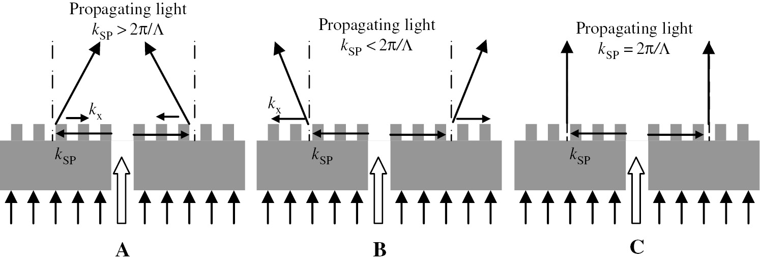
Schematic diagram of beaming effect through subwavelength metallic slits for the three cases of (A) kSP>2π/Λ, (B) kSP<2π/Λ, and (C) kSP=2π/Λ.
Different beam control such as divergence and convergence can be realized in the different cases.
2 Theoretical background and design of metalens
It is well known that the following condition needs to be satisfied for the purpose of exciting SPP waves through a subwavelength corrugated periodic metallic structure.
where, n0 is the refractive index of the incident medium, normally, air; k0 is the wave vector of the incident beam; θ is the incident angle; and m is an integer (m=0, 1, 2, 3…). For the special case of kSP=2π/Λ, it is only applicable when the incident angle θ=0° and m=1. Our metalens is designed based on this consideration.
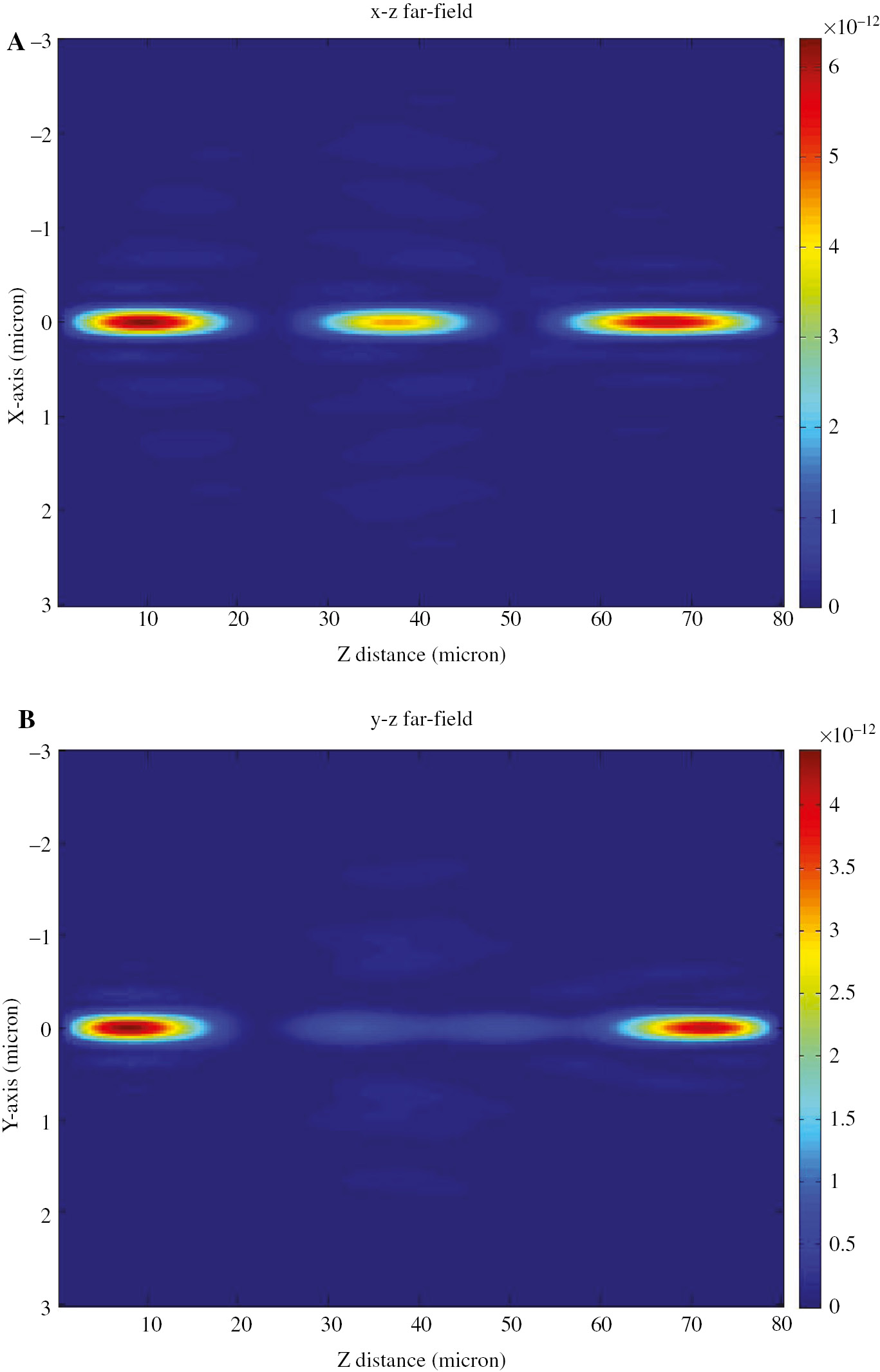
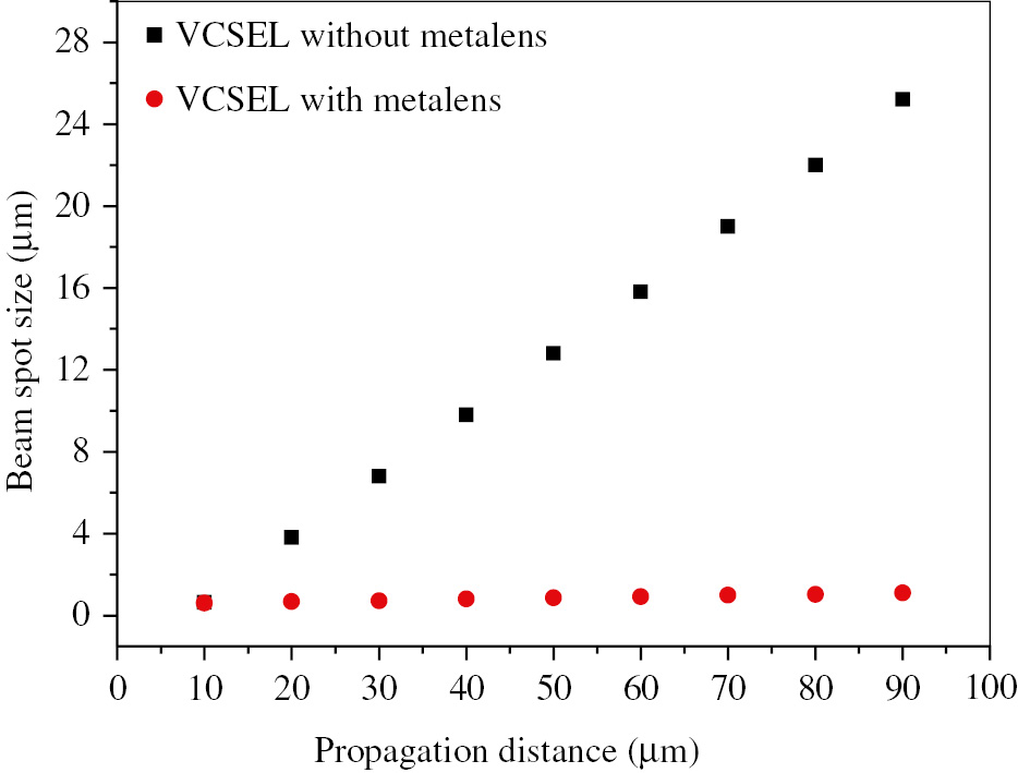
The beaming structure discussed here is composed of a subwavelength aperture (300 nm in diameter) in a gold thin film of 200 nm in thickness with surface gratings on the exiting plane (see Figure 1). The corrugation period used for the design is 980 nm with a duty cycle of 1:1. Considering the application issue, the working wavelength of 980 nm is set in the finite domain and time difference (FDTD) (FDTD Solution software: Lumerical Solutions Inc., Vancouver, Canada) algorithm-based simulation. The PML boundary condition is applied in the FDTD simulation with meshing size of 2 nm in the x-, y-, and z-directions. Figure 2 is the beaming effect of the designed metalens at near field for the special case of kSP=2π/Λ in vertical planes of x-z and y-z, respectively. It can be seen that neither beam divergence nor convergence is observed in the near-field intensity distribution. To further check the beaming effect, we calculated the corresponding intensity distribution in the far-field region, as shown in Figure 3. As can be seen, the beam spot size is nearly the same along the propagation distance of several microns, which is close to emitting surface, to as far as the distance of z=80 μm (they are also quantitatively evidenced in Figure 4 below). In order to compare the beaming size, we calculated the two-dimensional intensity profiles along the x- and y-axis in both the near- and far-field regions, as shown in Figure 4A and B. It can be seen that the beam sitting at full width half maximum (FWHM) is unchanged in the far field along the propagation distance ranging from z=5 μm to z=75 μm. However, FWHM is slightly large along the y-axis in the near field (see Figure 4B) compared to that of the far field due to the excited SPPs wave (linear y-polarization of the incident beam), which mixes together with the propagation beam in free space. The energy portion of the SPPs wave, ISPP/ISPP+Ifree≈40% for the wavelength of 980 nm (see Figure 17 in Ref. [19]). However, FWHM is apparently larger than that of the y-axis along the x-axis because of no SPP confinement along this direction. Therefore, we can answer the previous question now on the basis of the calculation results. A collimation beam can be obtained in the special case of kSP=2π/Λ. The discovery is quite useful for a lot of practical applications such as MOEMS, endoscopy, micro-total analyzing systems (μTAS), and light detection and ranging (LIDAR) systems.
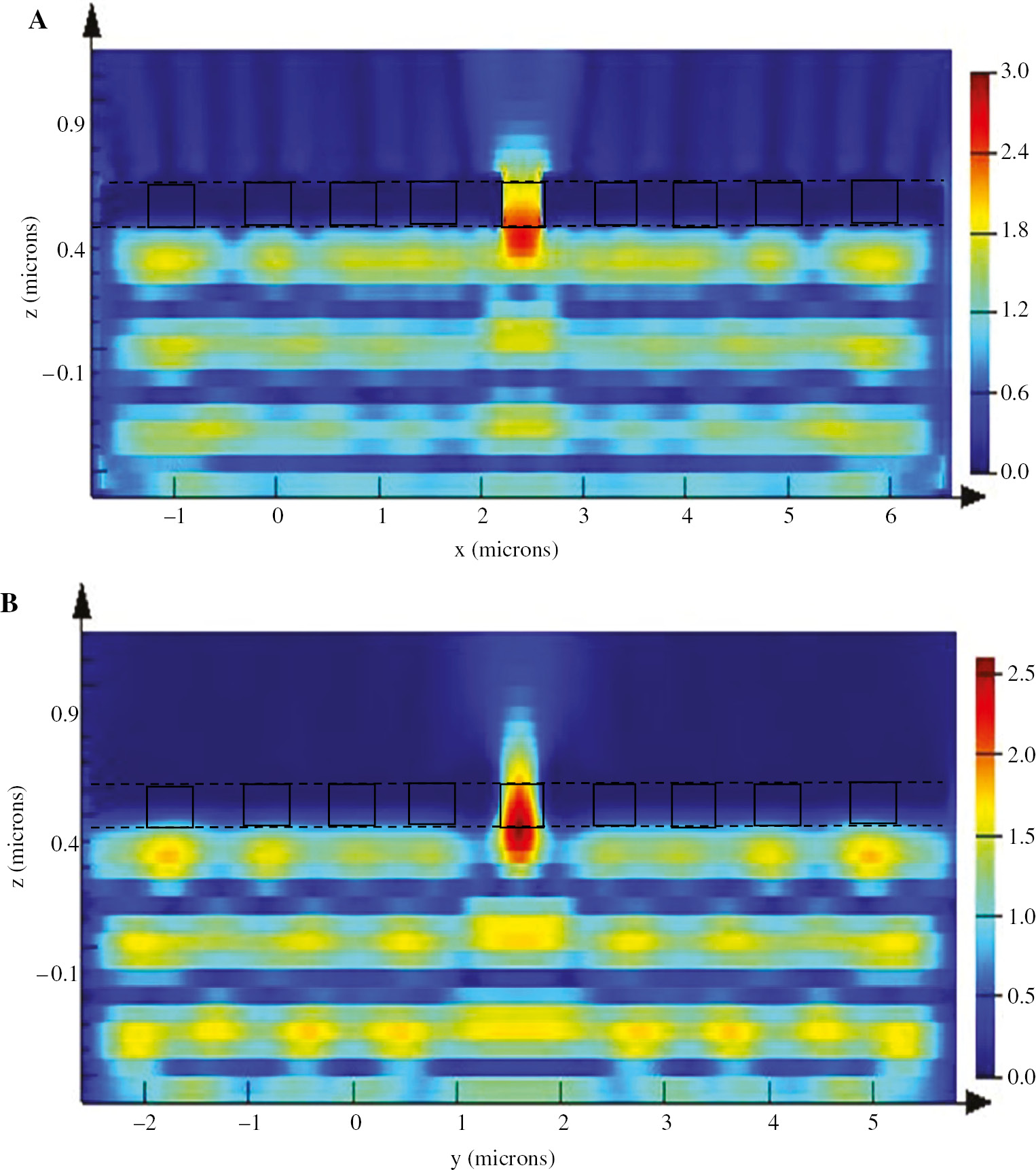
E-field intensity distribution of the metalens in free space.
It shows beaming effect of the designed metallic structure at near field for the special case of kSP=2π/Λ at vertical planes of x-z and y-z, respectively.
E-field intensity distribution of the metalens in free space.
It shows beaming effect of the designed metallic structure at far field for the special case of kSP=2π/Λ at vertical planes of x-z and y-z, respectively. Interference between the collimated emitting beam and SPP waves occurs in free space. This is the reason why some focusing spots are observed at some intervals instead of a conventional continuously distributed collimated beam in the far-field of micron scale distance. The interference will disappear in the region of millimeter scale because intensity of the SPP wave decays to be zero already in this region.
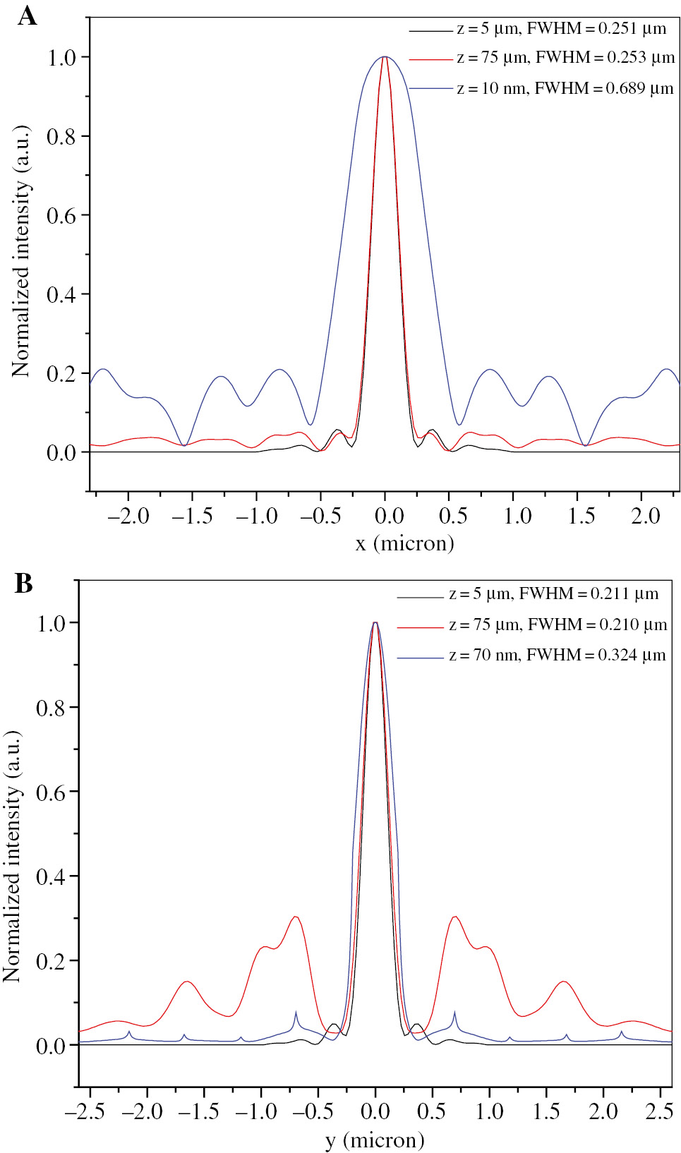
Two-dimensional E-field intensity profiles of the metalens along different propagation distances of z=10 nm, 5 μm and 75 μm in both (A) x-axis and (B) y-axis.
3 Experimental setup and typical application
The VCSEL chip was fabricated outside the company using the standard process. VCSEL is a type of important semiconductor laser with unique features of circular output beam and testing on wafer level due to the surface emission. Therefore, integration together with a VCSEL on wafer level is more convenient, which is important for miniaturization of the micro-optical systems, for example, integration of photonic crystals [20], micro-diffraction lens [21], and radial slits integrated with a VCSEL for polarization modulation [22]. Fabrication of VCSEL is mature in the industry. The detailed fabrication procedures are reported in Ref. [23]. The dimension of the metalens matches the aperture size of the VCSEL. This feature makes the metalens a good candidate for the purpose of integration and beam correction. Considering this, we put forth a scheme of an integration between the metalens and VCSEL.
To experimentally verify the beaming effect, as an application example, we apply the designed metalens onto a VCSEL, as shown in Figure 5. Theoretically, the divergent VCSEL beam can be compressed greatly by the metalens. The working wavelength of the VCSEL is 980 nm. Before focused ion beam (FIB) machining, the apertures of the VCSEL are coated with an Au thin film of 200 nm in thickness using photolithographic technique, as shown in Figure 6A and B. Then, the metalens is directly fabricated using FIB direct milling on the Au film, as shown in Figure 6C. An experimental setup is built for the purpose of testing the performance of the integrated VCSEL and beaming effect after passing through the metalens, as shown in Figure 7A. In this figure, the 3D stage 2 functions as precisely controlling the working distance between the scan head detector and the metalens for the purpose of calculating the divergence angle of the emitting beam. The system can collect the data from the free space of the metalens. A MATLAB (Mathworks Inc., USA) program is written so as to directly plot the I-V curve using the collected data in the computer. Beam profile and FWHM can be known from the beam profiler (PicoScope oscilloscope: Pico Technology, Cambridgeshire, UK). The current is injected through the two metal probes, as shown in Figure 7B.
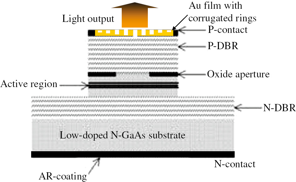
Schematic diagram of integration of VCSEL and the metallic structure, which is directly caped onto the emitting aperture of VCSEL.
Working wavelength of the VCSEL is 980 nm.
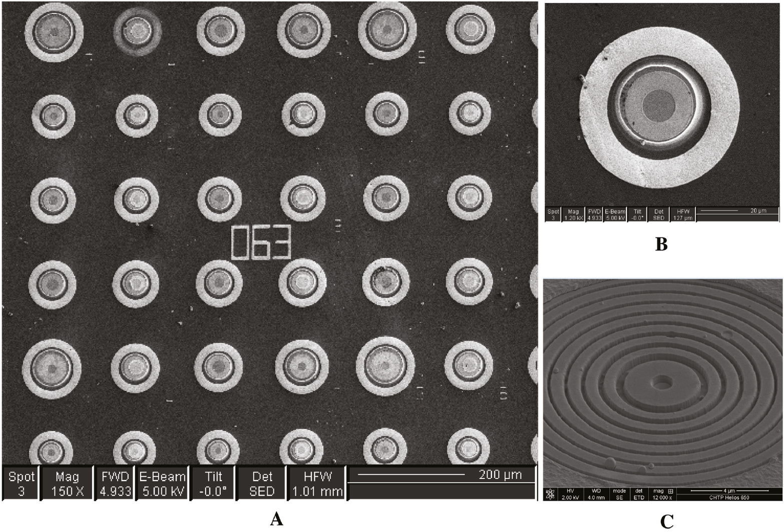
FIB Fabrication results of (A) SEM micrograph of the VCSEL array on wafer before integration, (B) zoom-in picture of a single VCSEL before integration, (C) after integration of the metalens through FIB milling.
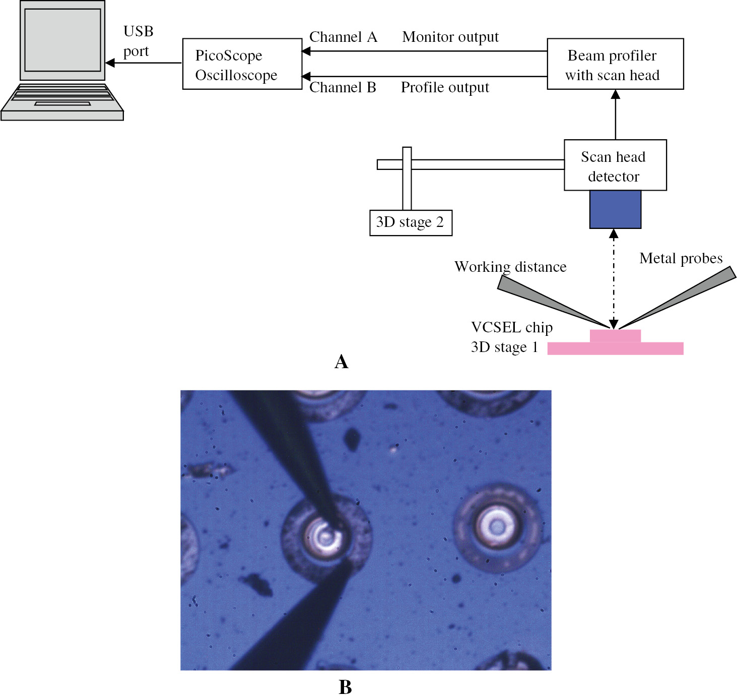
Experimental setup for (A) beam profile measurement of the metalensed VCSEL; (B) probing the lens.
To evaluate the performance of the integrated VCSEL, we measured the beam spot size in the far field first, as shown in Figure 8. It can be seen that the far-field angle (half divergence angle) measured by a PicoScope oscilloscope beam scanner is calculated in terms of the beam spot size and the corresponding interval distances are 0.2° and 9° with and without the integrated metalens, respectively. To further evaluate the VCSEL performance, we tested the P-I and I-V curves before and after the integration, as shown in Figure 9A and B. As can be seen, the power of the metalensed VCSEL linearly increases with increasing injection current. For the I-V curve, it is approximately linearly increasing when the injection current is larger than 1 mA. The calculated Q factor of the integrated VCSEL is 5780. The results demonstrate that the metalensed VCSEL is capable of emitting a collimation beam in the far-field region. It is promising for the miniaturization of some optical systems such as LIDAR system and endoscopy.
Probing results with injection current of 3 mA, far-field angle (half divergence angle) measured by a PicoScope oscilloscope beam scanner, the angles calculated in terms of incline angle of the lines are 0.4° and 18° with and without the integrated metalens, respectively.
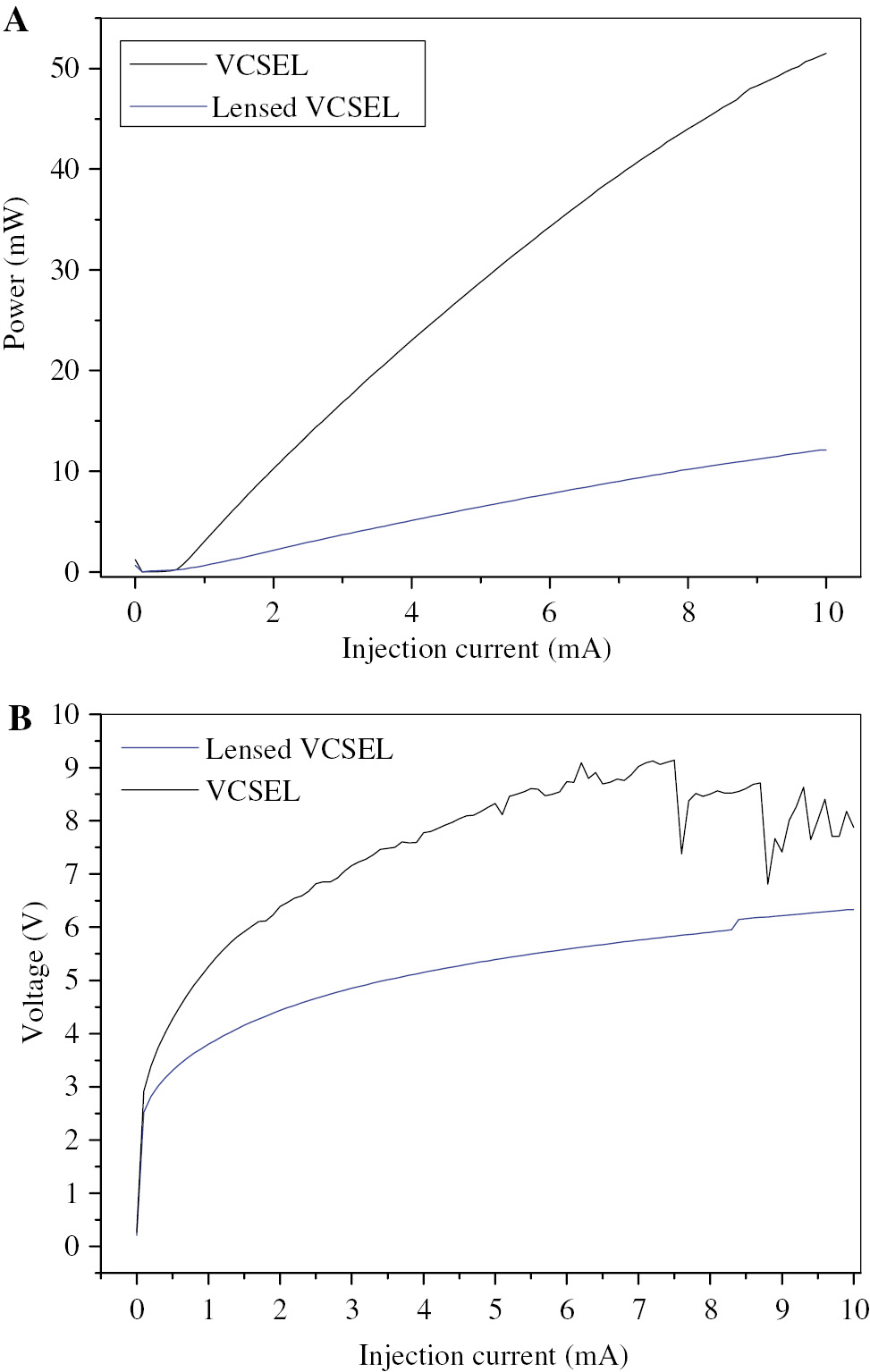
Comparison of characteristics of the VCSELs with and without the metalenses.
(A) P-I curves before and after the integration. (B) I-V curves before and after the integration.
4 Summary
In summary, an anomalous beaming effect of the periodic metallic corrugations for a special case of kSP=2π/Λ is analyzed and verified by means of both theoretical calculation and experimental probing. The design results show that the metalens can realize the beaming of collimation in a far-field region. As a typical application example, the designed metalens is integrated together with a VCSEL on the top surface of the emitting aperture. The full beaming angles calculated on the basis of the beam spot sizes measured in the far-field region are 0.4° and 18° with and without the integrated metalens, respectively. Further performance testing results of the P-I and I-V curves demonstrate that the metalensed VCSEL is applicable for practical use.
Acknowledgment
This work is supported by the National Scientific Foundation of China with approved number of U1532133.
References
[1] Ritchie RH. Plasma losses by fast electrons in thin films. Phys Rev 1957;106:874–81.10.1103/PhysRev.106.874Search in Google Scholar
[2] Martin-Moreno L, García-Vidal FJ, Lezec HJ, Degiron A, Ebbesen TW. Theory of highly directional emission from a single subwavelength aperture surrounded by surface corrugations. Phys Rev Lett 2003;90:167401.10.1103/PhysRevLett.90.167401Search in Google Scholar PubMed
[3] Ebbesen TW, Lezec HJ, Ghaemi HF, Thio T, Wolff PA. Extraordinary optical transmission through subwavelength hole arrays. Nature 1998;39:667–9.10.1038/35570Search in Google Scholar
[4] Zakharian AR, Moloney JV, Mansuripur M. Surface plasmon polaritons on metallic surfaces. Opt Express 2006;15:183–97.10.1364/OE.15.000183Search in Google Scholar
[5] Fu Y, Zhou W, Lennie LEN, Du C. Plasmonic microzone plate: superfocusing at visible regime. Appl Phys Lett 2007;91:061124.10.1063/1.2769942Search in Google Scholar
[6] Lockyear MJ, Hibbins AP, Sambles JR. Surface-topography-induced enhanced transmission and directivity of microwave radiation through a subwavelength circular metal aperture. Appl Phys Lett 2004;84:2040.10.1063/1.1688001Search in Google Scholar
[7] Xie Y, Zakharian AR, Moloney JV, Mansuripur M. Transmission of light through periodic arrays of sub-wavelength slits in metallic hosts. Opt Express 2006;14:6400–13.10.1364/OE.14.006400Search in Google Scholar PubMed
[8] Treacy MMJ. Dynamical diffraction explanation of the anomalous transmission of light through metallic gratings. Phys Rev B 2002;66:195105.10.1103/PhysRevB.66.195105Search in Google Scholar
[9] Lerman GM, Yanai A, Levy U. Demonstration of nanofocusing by the use of plasmonic structures illuminated with radially polarized light. Nano Lett 2009;9:2139–43.10.1021/nl900694rSearch in Google Scholar PubMed
[10] Zhang H, Zhu J, Zhu Z, Li Q, Jin G. Surface-plasmon-enhanced GaN-LED based on the quasi-symmetrical planar waveguide structure. Opt Commun 2013;311:311–6.10.1016/j.optcom.2013.08.078Search in Google Scholar
[11] Zhang H, Zhu J, Zhu Z, Jin Y, Li Q, Jin G. Surface-plasmon-enhanced GaN-LED based on a multilayered M-shaped nano-grating. Opt Express 2013;21:13492–501.10.1364/OE.21.013492Search in Google Scholar PubMed
[12] Caldwell JD, Lindsay L, Giannini V, et al. Low-loss, infrared and terahertz nanophotonics using surface phonon polaritons. Nanophotonics 2015;4:44–68.10.1515/nanoph-2014-0003Search in Google Scholar
[13] Pacheco-Pena V, Minin IV, Minin OV, Beruete M. Comprehensive analysis of photonic nanojets in 3D dielectric cuboids excited by surface plasmons. Ann Phys (Berlin) 2016;528:684–92.10.1002/andp.201600098Search in Google Scholar
[14] Minin IV, Minin OV. Diffractive Optics and Nanophotonics: Resolution Below the Diffraction Limit. Berlin, Springer, 2016.10.1007/978-3-319-24253-8Search in Google Scholar
[15] Pacifici D, Lezec HJ, Atwate HA. Quantitative determination of optical transmission through subwavelength slit arrays in Ag films: role of surface wave interference and local coupling between adjacent slits. Phys Rev B 2008;77:115411.10.1103/PhysRevB.77.115411Search in Google Scholar
[16] Yu L-B, Lin D-Z, Chen Y-C, et al. Physical origin of directional beaming emitted from a subwavelength slit. Phys Rev B 2005;71:041405.10.1103/PhysRevB.71.041405Search in Google Scholar
[17] Kim YE. Preparation of piezoresistive nano smart hybrid material based on grapheme. Appl Phys Lett 2008;92:013103.10.1063/1.2828716Search in Google Scholar
[18] Yu N, Fan J, Wang QJ, et al. Small-divergence semiconductor lasers by plasmonic collimation. Nat Photonics 2008;2: 564–70.10.1038/nphoton.2008.152Search in Google Scholar
[19] García de Abajo FJ. Colloquium: light scattering by particle and hole. Rev Mod Phys 2007;79:1267–90.10.1103/RevModPhys.79.1267Search in Google Scholar
[20] Samakkulam K, Sulkin J, Giannopoulos A, Choquette KD. Micro-fluidic photonic crystal vertical cavity surface emitting laser. Electron Lett 2006;42:6–7.10.1109/LEOSST.2006.1693984Search in Google Scholar
[21] Fu Y, Bryan NKA. Investigation of micro-diffractive lens with continuous relief with vertical-cavity surface emitting lasers using focused ion beam direct milling. IEEE Photonics Technol Lett 2001;13:424–6.10.1109/68.920738Search in Google Scholar
[22] Bin-Zong X, Jie-Tao L, Li-Kang C, et al. The generation of a compact azimuthally polarized vertical-cavity surface emitting laser beam with radial slits. Chin Phys Lett 2013;30:034206.10.1088/0256-307X/30/3/034206Search in Google Scholar
[23] Das NC, Hsen H, Newman P, Lara MT, Chang W. Design and Fabrication of 850 and 980 nm Vertical Cavity Surface Emitting Laser. Adelphi, MD 20783-1197: Sensors and Electron Devices Directorate, ARL, 2004.10.21236/ADA423231Search in Google Scholar
©2017 Yongqi Fu et al., published by De Gruyter, Berlin/Boston
This work is licensed under the Creative Commons Attribution-NonCommercial-NoDerivatives 4.0 License.
Articles in the same Issue
- Review articles
- Advances in optoplasmonic sensors – combining optical nano/microcavities and photonic crystals with plasmonic nanostructures and nanoparticles
- Periodic array-based substrates for surface-enhanced infrared spectroscopy
- From isolated light-harvesting complexes to the thylakoid membrane: a single-molecule perspective
- Theory and applications of toroidal moments in electrodynamics: their emergence, characteristics, and technological relevance
- Multiple exciton generation in quantum dot-based solar cells
- All-integrated terahertz modulators
- Exciton-plasmon coupling interactions: from principle to applications
- Emerging technologies for high performance infrared detectors
- Research articles
- Magneto-optical response in bimetallic metamaterials
- Saturated evanescent-wave absorption of few-layer graphene-covered side-polished single-mode fiber for all-optical switching
- Reversible thermochromic response based on photonic crystal structure in butterfly wing
- Selection rule engineering of forbidden transitions of a hydrogen atom near a nanogap
- Heterogeneous terahertz quantum cascade lasers exceeding 1.9 THz spectral bandwidth and featuring dual comb operation
- Effect of temperature on the structural, linear, and nonlinear optical properties of MgO-doped graphene oxide nanocomposites
- Engineering light emission of two-dimensional materials in both the weak and strong coupling regimes
- Anisotropic excitation of surface plasmon polaritons on a metal film by a scattering-type scanning near-field microscope with a non-rotationally-symmetric probe tip
- Achieving pattern uniformity in plasmonic lithography by spatial frequency selection
- Controllable all-fiber generation/conversion of circularly polarized orbital angular momentum beams using long period fiber gratings
- High-efficiency/CRI/color stability warm white organic light-emitting diodes by incorporating ultrathin phosphorescence layers in a blue fluorescence layer
- Relative merits of phononics vs. plasmonics: the energy balance approach
- Efficiency enhancement of InGaN amber MQWs using nanopillar structures
- Color display and encryption with a plasmonic polarizing metamirror
- Experimental demonstration of an optical Feynman gate for reversible logic operation using silicon micro-ring resonators
- Specialized directional beaming through a metalens and a typical application
- Anomalous extinction in index-matched terahertz nanogaps