The Dublin lens: a Cc = 1.0 mm objective lens intended for CryoEM at 100 keV
-
Germano Motta Alves
 ,
Theo Andrews
,
Patrick McBean
,
Torquil Wells
,
Mohamed M. El-Gomati
,
Stephan Burkhalter
,
Clemens Schulze-Briese
,
Pietro Zambon
,
Greg McMullan
,
Theo Andrews
,
Patrick McBean
,
Torquil Wells
,
Mohamed M. El-Gomati
,
Stephan Burkhalter
,
Clemens Schulze-Briese
,
Pietro Zambon
,
Greg McMullan
 ,
Richard Henderson
,
Christopher J. Russo
and
Lewys Jones
,
Richard Henderson
,
Christopher J. Russo
and
Lewys Jones

Abstract
We have designed, fabricated and tested a lens with a chromatic aberration coefficient (Cc) of 1.0 mm, a 4.0 mm pole-gap and 2.0 mm bore that is wide enough to accommodate an anti-contamination system and an objective aperture. This lens extends the temporal-coherence envelope of the electron microscope beyond 2 Å, using a low-cost Schottky FEG. We hope that this lens design can be used to improve all 100 keV electron microscopes designed for single-particle electron cryomicroscopy (cryoEM).
1 Introduction
The primary method for determining the structure of biological molecules has recently become single-particle cryoEM [1]. Previous work has shown that 100 keV electrons have the potential to improve structure determination by cryoEM since there is more information in the images at 100 keV per unit damage than at higher energies [2], [3]. Recent work has demonstrated that structure determination by cryoEM at 100 keV is both possible and practical [4], [5], [6], [7]. Furthermore, two hardware modifications were identified in [4] that can offer improvement in microscope performance with minimal increases in cost:
Modification of the objective lens to reduce the effects of chromatic aberration, which increases the signal at high resolution.
Modification of the detector to increase the number of pixels, such that the detective quantum efficiency at a particular resolution can be increased using magnification.
In this work, we address the first of these. Given the growth of cryoEM and the ever-increasing cost of high-end microscopes, there is still a desperate need for affordable microscopes capable of structure determination and walk-up assessment of specimens. Interestingly, improving the objective lens performance does not increase the complexity of the microscope and so has the potential to enable higher performance without increasing their cost.
Transmission electron microscope (TEM) objective lenses consist of a (typically) copper coil which produces the excitation, a ‘yoke’ which guides the flux to complete the magnetic circuit, and a pole-piece with a fixed bore and gap that dictate the shaping of the magnetic field in the focussing region. A simplified illustration of such a lens is shown in Figure 1.
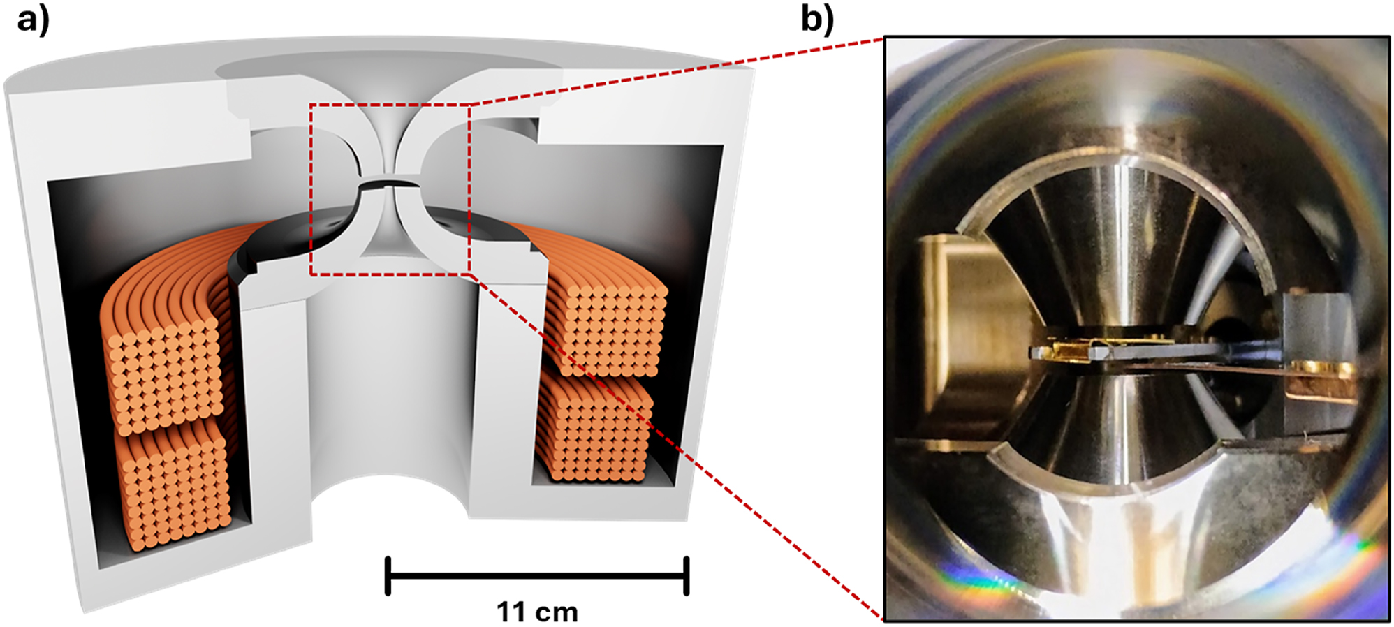
(a) Illustration of a transmission electron microscope objective-lens; showing the copper wire coils, outer magnetic circuit, and pole-piece with pole-gap. (b) Photograph of the Dublin lens installed in a JEOL 1400/HR at the MRC-LMB. The specimen rod is visible extending from the rear on the right. The objective aperture strip extends from the front on the right.
Such TEM objective lenses are normally designed to minimise Cs [8], [9]. Minimisation of Cs tends concurrently to minimise Cc as the two are coupled to the geometry of the pole piece [10], [11], [12], [13]. Notable exceptions include lenses designed for aberration-corrected systems [14], [15], which are normally operated with room-temperature specimens. Cc values for previous lenses range from 0.6 mm to 4.0 mm [16]. Designs with Cc less than 2 mm are rare and inevitably are designed for room temperature or ultra-high-vacuum columns [14]. Microscopes designed for cryoEM have Cc in the range 2–3 mm (e.g. Krios, CRYO-ARM, Polara), often to accommodate the wide gaps needed for a tight cryobox around the specimen while retaining the ability to tilt the grids as much as possible. Here, by eliminating the requirement for tilting the specimen, optimising specifically for Cc only and maintaining as wide a gap as possible, we have a new set of design constraints that are specific for improving single particle cryoEM.
2 Methods
2.1 Approach
Here we sought to design a lens suitable for accommodating a liquid nitrogen cooled anti-contaminator system and standard cryo-specimen holders without touching the pole-piece which is kept at room temperature.
2.2 Design
To evaluate the performance of many lens geometries in parallel, a genetic algorithm (GA) tailored specifically for bespoke pole-piece design was written [17]. The GA is a metaheuristic that relies on the theory of natural selection, wherein the members of a population with the most favourable traits are the most likely to survive and reproduce. The algorithm emulates this by preserving the best-performing geometries, creating mutants and crossovers of high- and mid-ranked geometries, and discarding the worst candidates [18]. Performance was evaluated with a fitness function, specified by the user in accordance with the desired lens properties. Such a GA approach has previously been successfully implemented in magnetic and electrostatic lens design for objectives, electron guns and even MRI machines [19], [20], [21], [22], [23], [24].
Beginning with a Python-defined vectorised description of a stylised pole-piece geometry, various randomised mutations of the geometry were performed to create a population of candidates. Each candidate was used as the input for a magnetic flux simulation using COMSOL Multiphysics®. The resulting magnetic flux profile along the optic axis was used as the input to a Julia script to determine values of the chromatic aberration coefficient (Cc) as well as spherical aberration (Cs) and focal length. These values were substituted into a fitness function, in our case prioritising Cc, and the candidates were then ranked from best to worst. This ranking was used to create a new generation of geometries, say by eliminating the worst-ranked half, followed by crossover and mutation of the remainder. The calculations continued in this iterative manner until the specified number of generations was reached.
Simulated aberration coefficients were calculated at a particular value of coil excitation just below magnetic saturation. This was obtained by evaluating the paraxial magnetic flux profile at two boundary excitation values to find the position of the image plane, which was above and below zero for the respective boundary values. Using these values as a starting point, paraxial flux analysis was performed iteratively at halfway points between boundary image plane positions until the coil excitation, for which the image plane lies at zero, i.e. the saturation excitation, was obtained. This value was used to calculate the final aberration coefficients utilised in the GA’s fitness function.
For this work, the GA was driven by a fitness function which prioritised the minimisation of Cc over Cs or focal length. The fabrication-ready design resulted from the evaluation of 250 generations, each comprised of 250 candidates, with minor adjustments made to the curvature of the pole-pieces for machining feasibility. The simulated physical and aberration properties of the lens are displayed in Table 1, alongside the values measured and described later in this paper. Some further examples of various calculated aberrations for different geometries are given in the Supplementary material.
Design parameters and simulated properties (left) and the measured values (right).
| Property (mm) | Specification/simulation | Measured |
|---|---|---|
| Bore | 2.00 mm | 1.993 mm (±0.003) |
| Pole gap | 4.00 mm | 4.017 mm (±0.003) |
| Cc | 1.015 mm | 0.97 mm (±0.02) |
| Cs | 0.76 mm | 0.62 mm (±0.05) |
| Focal length | 2.43 mm | – |
2.3 Fabrication
Pole-pieces were fabricated in Ireland with assistance from Irish Manufacturing Research, a national centre of excellence and training in advanced manufacturing. Upper and lower poles were fabricated from an iron-cobalt alloy and a non-magnetic spacer placed between each pole. The complete pole-piece was heat-treated to obtain optimal magnetic properties before dimensional analysis was performed using a coordinate measuring machine (CMM).
Before installation, the pole-piece was cleaned using an ultrasonic bath with sequential rinses of CMOS-grade acetone (x1) and isopropyl alcohol (x3) followed by air drying in a laminar flow clean hood. The original JEOL pole-piece was removed through the TEM’s pole-piece access port, and the new design was lowered in its place using a bespoke installation tool. The original goniometer and aperture strip were replaced, and the column pumped.
2.4 Testing
The lens was installed on a standard JEOL 1400/HR microscope, which was equipped with two important modifications, namely a prototype hybrid pixel detector from DECTRIS and a Schottky FEG electron source from York Probe Sources.
The hybrid pixel detector was an experimental prototype that uses a gallium arsenide (GaAs) wafer as its sensitive layer with sub-50 μm pixels bump-bonded to the ASIC event counting architecture below, which consists of juxtaposed ASICs. The ion-pairs created by the electron track are collected by a voltage bias and converted into electron events that are read out at kHz frame rate. This gives the detector superb performance for its megapixel field-of-view, but a full description of its performance and properties are beyond the scope of this paper.
The field emission gun (FEG) from YPS is also a prototype. It represents a further improvement in terms of stability and reliability of the earlier design [25], used previously to demonstrate the promise of structure determination by cryoEM at 100 keV [4]. The most recent improvement involves the use of an improved high-voltage ceramic material and improved mechanical alignment designs in the FEG.
After installation of the lens, the illumination system was realigned by adjustment of the beam tilt to minimise the image motion by observing the rotation centre using the objective lens current wobbler. A Zemlin tableau would be useful to provide further characterisation and is planned soon [26].
Cc measurement was made by recording a series of images at a nominal magnification of 300 kX corresponding to a pixel size of 0.74 Å at the specimen, which was calibrated from the (111) fringes of the gold nanoparticles at 2.35 Å. The accelerating voltage was changed to be 30 V above and 30 V below the 100,000 V operating value in 30 V steps in both directions to eliminate any possibility of hysteresis. As in the earlier work [4], the voltage calibration was checked. The slope of defocus versus accelerating voltage gives Cc directly (Figure 2a), using the formula Cc = (ΔF/ΔE)*E, where (ΔF/ΔE) is the slope and E is the accelerating voltage, and was found to be 0.97 mm.

(a) Measurement of Cc from change in underfocus as a function of electron energy; error bars on defocus are small. (b) Measurement of Cs by least-squares fitting of three CTF parameters shown in the box. The specimen was a carbon/gold/carbon sandwich.
Cs was estimated from a 300 kX magnification image (pixel size of 0.74 Å) of gold on carbon using the same C/Au/C sandwich specimen as used for Figure 3b, but with an exposure time of 40 s, corresponding to 256,000 frames. Multiple sub-frame (2048) summations were then aligned by cross-correlation to compensate for slight specimen drift during the full exposure to give a final image that showed good resolution in all directions. Small amounts of differential magnification or astigmatism were then eliminated computationally to give the radial power spectrum shown in Figure 2b. The values of defocus, Cs and amplitude contrast were then minimised computationally to produce the best agreement between the observed and fitted radii of the contrast transfer function (CTF) zeroes.

(a) Young’s fringes FFT of the sum of a pair of PtIr images extending well beyond 2 Å. The images added together were 2025_03_06–21_31_03 and 2025_03_06–21_31_42. (b) FFT of gold in a carbon sandwich showing the 2.3, 2.0, 1.4 and 1.2 Å lattice fringes from Au (111), (200), (220), and (311) spacings in image 2025_03_19-17_55_02. Images were recorded at a nominal magnification of 400 kX using a DECTRIS prototype detector, with a calibrated pixel size of 0.55 Å at the specimen. The resolution at the edge of the image is 1.1 Å and the dashed circle is at 1.5 Å.
The two images shown in Figure 3 were recorded with slightly higher magnifications (nominally 400 kX, with a calibrated pixel size of 0.55 Å at the specimen). Figure 3a was made by adding together two images of amorphous platinum/iridium (Agar Scientific) recorded 40 s apart during which the specimen had drifted by about 35 Å, creating an electron imaging equivalent of the Young’s fringe experiment [27]. The fringes show good resolution beyond 2 Å. Figure 3b shows the FFT of an image of a specimen of gold nanoparticles sandwiched between thin films of amorphous carbon. This was made by floating carbon off mica, then evaporating gold followed by a final coating of carbon to create a C/Au/C sandwich in which the gold domain orientations were more stable than on a single layer. The real-space image is shown in Supplementary material Figure S1.
3 Results
We determined Cc at 100 keV by measuring the slope of defocus versus accelerating voltage (Figure 2a). Cc was 1.01 mm with the stage at a height of Z = 350 μm (Obj current 3.35 A). Cc was 0.97 mm (±0.02) with the stage at the lower height of Z = 150 μm (Obj current 4.02 A). The JEOL 1400 lens power supply did not allow enough current to obtain an in-focus image with the stage height lower than Z = 150 μm (Objective lens current 4.10 A is the current maximum), but this could be easily fixed with simple changes to the lens power supply.
Cs was estimated by fitting the CTF to the Fourier transform of an image of sputtered gold sandwiched between two thin films of amorphous carbon. Cs was found to be 0.61 mm, as shown in Figure 2b. The agreement between the observed and calculated CTF zeroes was not perfect but there were two mitigating factors, one experimental and one theoretical, that could explain the deviation. Experimentally, the C/Au/C specimen was made by floating the first layer of carbon off mica so it should be very flat. Gold nanoparticles were then sputtered onto the carbon film before coating with a second layer of carbon. Thus, the gold may have a slightly different height (possibly by ∼50 Å) than the carbon. A defocus change from 823 Å to 800 Å would cause a shift of the CTF zeroes by the small amount observed. Theoretically, it is also known that the amplitude contrast for elastic scattering from gold is much higher than for carbon. For example, Erickson and Klug showed [28] that uranyl acetate had 35 % amplitude contrast, whereas carbon has only about 10 %. Such a variation would also cause a shift in the CTF zero positions for the gold fringes. A similar value for Cs of 0.62 (±0.05) mm was obtained using images of a pure carbon film (see Supplementary material), with a closer fit but over a smaller range because the Thon rings from the carbon film extended only to about 2.5 Å.
The performance of the lens was demonstrated by recording images of amorphous PtIr displayed using the Young’s fringe approach (Figure 3a, see legend) and gold sputtered on a thin film of amorphous carbon (Figure 3b), showing the lattice spacings expected from the gold nanoparticles.
4 Discussion
Most previous objective lens designs have given priority to reducing Cs. Here, we prioritised reducing Cc, since in cryoEM Cs is already fully included in CTF correction for the defocused bright-field images that are essential to produce enough contrast. CryoEM also needs a wide enough pole-gap to allow space for an anti-contaminator. The lens described here with a 2 mm bore and 4 mm gap fulfils these goals.
The thickness (height) of some currently available specimen rods for the JEOL 1400/HR microscope, including their retractable cryo-shields, from Gatan, Simple Origin and Fischione, are 1.4–2.6 mm. These will easily fit into the 4 mm pole gap, allowing at least 0.5 mm above and below for a new anti-ice cryobox.
The cryobox on the original JEOL 1400/HR has a gap of ≈5 mm, which allows some specimen tilting. With our proposed smaller gap, there would be the possibility of limited specimen tilts (a few degrees). However, in our previous work on 11 different specimens [4], no specimen tilt was required, suggesting specimen tilting is an unnecessary compromise for single-particle cryoEM, and the lens design should instead be driven by aberration optimisation. Alongside optical developments, it remains important to have a stable cold stage and rapid cryo-transfer, which are features that are beyond the scope of this paper.
5 Conclusions
We have shown that it is possible to design, fabricate and test an objective lens for 100 keV microscopy that has a wide pole-piece gap, a reasonable bore, performance that agrees with expectations from simulations, and a resulting improvement of the signal at 2 Å resolution. We hope that this approach to designing a lens for cryoEM where minimum Cc is the key parameter while keeping costs down, will be adopted for all single-particle electron cryomicroscopes going forward.
Funding source: Medical Research Council
Award Identifier / Grant number: MC_UP_120117
Funding source: Irish Research Council
Award Identifier / Grant number: EPSPG/2024/1994
Funding source: Wellcome Trust
Award Identifier / Grant number: 220526/B/20/Z
Funding source: Science Foundation Ireland
Award Identifier / Grant number: 12/RC/2278 P2
Award Identifier / Grant number: URF/RI/191637
Funding source: Innovate UK
Award Identifier / Grant number: 103806
Acknowledgments
The authors would like to thank Maixent Cassagne for help testing the GA code during his internship, and Dr. Tomáš Radlička of the Czech Academy of Sciences for developing the Julia package with which the simulated aberration coefficients were calculated. The Trinity authors would like to thank Irish Manufacturing Research for their assistance in developing the high-precision manufacturing and dimensional metrology. We would like to thank Karl Gaff for the illustration of the objective lens, P. Nellist and N. Unwin for helpful discussions.
-
Research ethics: Not applicable.
-
Informed consent: Not applicable.
-
Author contributions: All authors have accepted responsibility for the entire content of this manuscript and approved its submission.
-
Use of Large Language Models, AI and Machine Learning Tools: None declared.
-
Conflict of interest: The authors declare the following interests: LJ is the CEO and co-founder of turboTEM Ltd. who, amongst other activities, manufacture bespoke TEM pole-pieces. GMA is a former Trinity College researcher now employed by turboTEM Ltd. TA is a PhD student jointly funded by Research Ireland and turboTEM Ltd.
-
Research funding: GMA and LJ acknowledge Research Ireland grant 12/RC/2278 P2 (AMBER 2), TA acknowledges Research Ireland grant EPSPG/2024/1994, and LJ acknowledges Research Ireland grant URF/RI/191637. CJR, GM and RH thank the Wellcome Trust for award of grant No. 220526/B/20/Z, together with valuable financial support from Astex and AstraZeneca. This work has also been supported by the Medical Research Council under Grant No. MC_UP_120117 (C.J.R.). We acknowledge early support for development of the FEG from Innovate UK Grant No. 103806.
-
Data availability: Not applicable.
References
[1] A. Patwardhan, R. Henderson, and C. J. Russo, “Extending the reach of single-particle cryoEM,” Curr. Opin. Struct. Biol., vol. 92, p. 103005, 2025.10.1016/j.sbi.2025.103005Search in Google Scholar PubMed
[2] M. J. Peet, R. Henderson, and C. J. Russo, “The energy dependence of contrast and damage in electron cryomicroscopy of biological molecules,” Ultramicroscopy, vol. 203, pp. 125–131, 2019. https://doi.org/10.1016/j.ultramic.2019.02.007.Search in Google Scholar PubMed PubMed Central
[3] K. Naydenova, et al.., “CryoEM at 100 keV: a demonstration and prospects,” IUCrJ, vol. 6, pp. 1086–1098, 2019. https://doi.org/10.1107/s2052252519012612.Search in Google Scholar PubMed PubMed Central
[4] G. McMullan, et al.., “Structure determination by cryoEM at 100 keV,” Proc. Natl. Acad. Sci. U. S. A., vol. 120, no. 49, Art. no. e2312905120, 2023.10.1073/pnas.2312905120Search in Google Scholar PubMed PubMed Central
[5] L. M. Chan, et al.., “High-resolution single-particle imaging at 100-200 keV with the Gatan Alpine direct electron detector,” J. Struct. Biol., vol. 216, no. 3, Art. no. 108108, 2024.10.1016/j.jsb.2024.108108Search in Google Scholar PubMed PubMed Central
[6] D. Karia, et al.., “Sub-3 Å resolution protein structure determination by single-particle cryo-EM at 100 keV,” bioRxiv preprint, 2024, https://doi.org/10.1101/2024.09.05.611417.Search in Google Scholar
[7] H. Venugopal, et al.., “High-resolution cryo-EM structures using a common LaB6 120-keV electron microscope equipped with a sub-200-keV direct electron detector,” Sci. Adv., vol. 11, no. 1, Art. no. eadr0438, 2025.10.1126/sciadv.adr0438Search in Google Scholar PubMed PubMed Central
[8] K. Tsuno and Y. Harada, “Design procedure for a high resolution electron microscope objective lens,” J. Electron Microsc., vol. 32, no. 4, pp. 289–298, 1983.Search in Google Scholar
[9] K. Tsuno, “Resolution limit of a transmission electron microscopy with an uncorrected conventional magnetic objective lens,” Ultramicroscopy, vol. 50, no. 3, pp. 245–253, 1993.10.1016/0304-3991(93)90193-2Search in Google Scholar
[10] G. Liebmann, “The magnetic electron microscope objective lens of lowest chromatic aberration,” Proc. Phys. Soc., Sect. B, vol. 65, no. 3, pp. 188–192, 1952.10.1088/0370-1301/65/3/303Search in Google Scholar
[11] P. W. Hawkes, Electron Optics and Electron Microscopy, London, Taylor & Francis Ltd., 1972, pp. 68–75.Search in Google Scholar
[12] K. Tsuno and D. A. Jefferson, “Design of an objective lens with a minimum chromatic aberration coefficient,” in Electron Microscopy and Analysis 1997, Proc. Inst. Phys. Conf. Ser. No. 153, Boca Raton, FL, USA, CRC Press, 1997, pp. 73–76.10.1201/9781003063056-17Search in Google Scholar
[13] K. Tsuno and D. A. Jefferson, “Design of an objective lens pole piece for a transmission electron microscope with a resolution less than 0.1 nm at 200 kV,” Ultramicroscopy, vol. 72, pp. 31–39, 1998.10.1016/S0304-3991(97)00125-3Search in Google Scholar
[14] O. L. Krivanek, P. D. Nellist, N. Dellby, M. F. Murfitt, and Z. Szilagyi, “Towards sub-0.5 Å electron beams,” Ultramicroscopy, vol. 96, pp. 229–237, 2003.10.1016/S0304-3991(03)00090-1Search in Google Scholar PubMed
[15] B. Kabius, et al.., “First application of Cc-corrected imaging for high-resolution and energy-filtered TEM,” J. Electron Microsc., vol. 58, no. 3, pp. 147–155, 2009.10.1093/jmicro/dfp021Search in Google Scholar PubMed
[16] M. A. O’Keefe, ““Resolution” in high-resolution electron microscopy,” Ultramicroscopy, vol. 47, pp. 282–297, 1992.10.1016/0304-3991(92)90203-VSearch in Google Scholar
[17] M. Cassagne, “Pole-piece design using genetic algorithm,” M.Sc. dissertation, Toulouse, France, Dept. Gen. Phys., Institut National des Sciences Appliquées Toulouse, 2024.Search in Google Scholar
[18] S. Katoch, S. S. Chauhan, and V. Kumar, “A review on genetic algorithm: Past, present, and future,” Multimed. Tools Appl., vol. 80, pp. 8091–8126, 2021.10.1007/s11042-020-10139-6Search in Google Scholar PubMed PubMed Central
[19] K. Höschel and V. Lakshminarayanan, “Genetic algorithms for lens design: A review,” J. Opt., vol. 48, pp. 134–144, 2019. https://doi.org/10.1007/s12596-018-0497-3.Search in Google Scholar
[20] N. H. M. Nezhad, M. Ghaffarian Niasar, A. Mohammadi Gheidari, C. W. Hagen, and P. Kruit, “Multi-electrode lens optimization using genetic algorithms,” Int. J. Mod. Phys. A, vol. 34, no. 36, Art. no. 1942020, 2019. https://doi.org/10.1142/s0217751x1942020x.Search in Google Scholar
[21] N. H. M. Nezhad, N. Ghaffarian, H. Mohamad, C. W. Hagen, and P. Kruit, “Tuning parameters in the genetic algorithm optimization of electrostatic electron lenses,” in Proc. 2023 IEEE MTT-S Int. Conf. Num. Elec. Multiphys. Model. Opt., Winnipeg, MB, Canada, IEEE, 2023, pp. 170–173.10.1109/NEMO56117.2023.10202293Search in Google Scholar
[22] A. Sabouri and C. S. Perez-Martinez, “Design of electrostatic lenses through genetic algorithm and particle swarm optimisation methods integrated with differential algebra,” Ultramicroscopy, vol. 266, Art. no. 114024, 2024. https://doi.org/10.1016/j.ultramic.2024.114024.Search in Google Scholar PubMed
[23] C. N. Ribton, “Development of an electron gun design optimisation methodology,” Ph.D. dissertation, London, UK, Dept. Elec. Comp. Eng, Brunel Univ., 2017.Search in Google Scholar
[24] J. S. Ryu, Y. Yao, C. S. Koh, and Y. J. Shin, “3-D optimal shape design of pole piece in permanent magnet MRI using parameterized nonlinear design sensitivity analysis,” IEEE Trans. Magn., vol. 42, no. 4, pp. 1351–1354, 2006. https://doi.org/10.1109/tmag.2006.871563.Search in Google Scholar
[25] M. M. El-Gomati, et al.., “100 keV vacuum sealed field emission gun for high resolution electron microscopy,” J. Vac. Sci. Technol., B:Microelectron. Process. Phenom., vol. 39, no. 6, Art. no. 062804, 2021, https://doi.org/10.1116/6.0001275.Search in Google Scholar
[26] F. Zemlin, K. Weiss, P. Schiske, W. Kunath, and K. H. Herrmann, “Coma-free alignment of high-resolution electron-microscopes with aid of optical diffractograms,” Ultramicroscopy, vol. 3, no. 1, pp. 49–60, 1978.10.1016/S0304-3991(78)80006-0Search in Google Scholar
[27] J. Frank, “Determination of source size and energy spread from electron micrographs using the method of Young’s fringes,” Optik, vol. 44, pp. 379–391, 1976.Search in Google Scholar
[28] H. P. Erickson and A. Klug, “Measurement and compensation of defocusing and aberrations by Fourier processing of electron micrographs,” Philos. Trans. R. Soc., B, vol. 261, no. 837, pp. 105–118, 1971.10.1098/rstb.1971.0040Search in Google Scholar
Supplementary Material
This article contains supplementary material (https://doi.org/10.1515/mim-2025-0019).
© 2025 the author(s), published by De Gruyter on behalf of Thoss Media
This work is licensed under the Creative Commons Attribution 4.0 International License.