
Elemental Two-Dimensional Materials Beyond Graphene
-
Udo Schwingenschlögl
 ,
Jiajie Zhu
,
Jiajie Zhu

Abstract
This review article summarizes a few of the papers presented during Symposium II of the International Conference of Pure and Applied Chemistry in July 2016. Properties of monolayers of silicene are first addressed, followed by multilayer silicene and, at the end, a discussion on germanene.
1 Silicene on substrates
As freestanding silicene has stability issues, understanding the effects of substrates becomes a critical task. Although the material (hexagonal structure) has been deposited successfully on various metallic substrates, including Ag [1], Ir [2], and ZrB2 [3], strong interaction perturbs the Dirac states and therefore must be avoided. Many semiconducting substrates, such as MgBr2 [4], WSe2 [5], MoS2 [6], and solid Ar [7], have been explored theoretically, predicting that the Dirac cone is preserved due to weak van der Waals interlayer interaction.
The lattice mismatches of MgBr2, WSe2, and MoS2, all having hexagonal structures, with silicene turn out to be small, see Table 1. Ar crystallizes in a cubic structure below 84 K so that the (111) surface is hexagonal and can support silicene. Configurations with different lateral shifts, as shown in Figure 1, have similar energies, the maximal differences amounting to 14 meV, 2 meV, 3 meV (high-buckled), and 32 meV (low-buckled) for MgBr2, WSe2, MoS2, and solid Ar, respectively, due to flat surface potentials. The interlayer distance is calculated to be more than 3.1 Å (Table 1), which reflects weak interaction and corresponds to the fact that the Si buckling height is slightly larger than in the case of freestanding silicene (0.47 Å). It has been reported for MoS2 that the structure relaxation depends critically on the van der Waals correction method [6, 8]. Both the DFT-D3 and optB86b-vdW methods can reproduce the experimental interlayer distance of 3.0 Å for high-buckled silicene, see Table 2. The corresponding values for low-buckled silicene are predicted to be 3.10 Å and 3.15 Å. The vdW-DF1, vdW-DF2, optPBE-vdW, and optB88-vdW methods, on the other hand, underestimate the interlayer interaction.
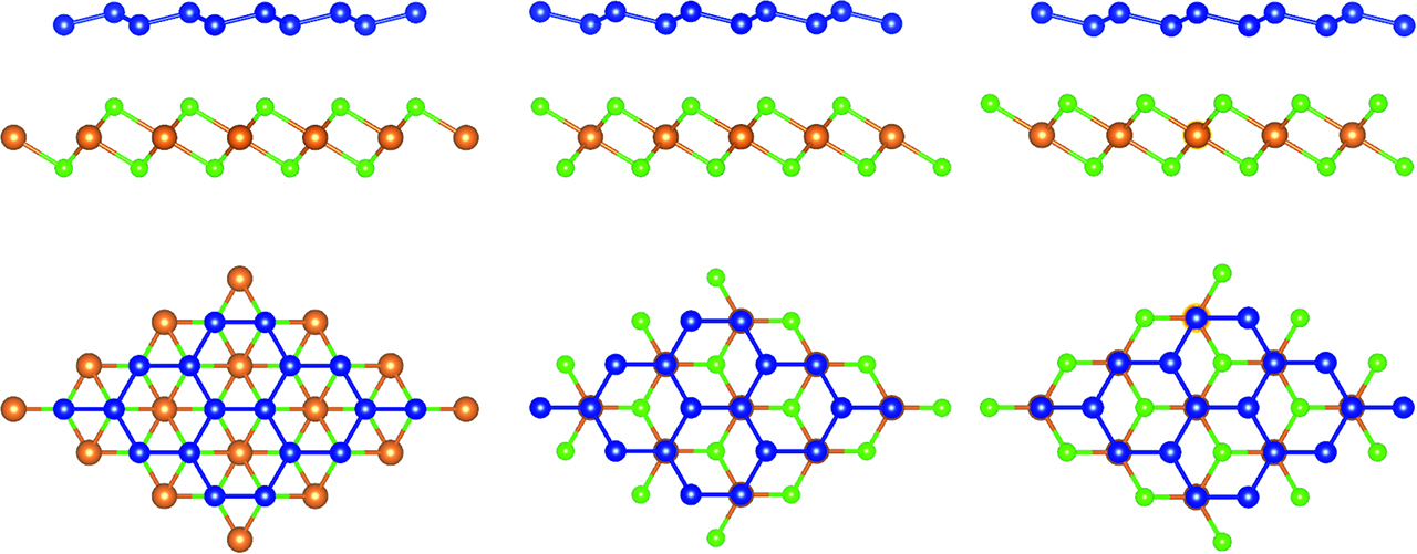
Top and side views of silicene on MgBr2 in different configurations. Mg, Br, and Si atoms are shown in brown, green, and blue color, respectively. Reprinted with permission from Zhu, J.; Schwingenschlögl, U. ACS Appl. Mater. Interfaces2014, 6, 11675-11681. Copyright 2014 American Chemical Society.
Structural and electronic parameters of silicene supported by MgBr2, WSe2, MoS2, and solid Ar, as calculated by the DFT-D3 method.
| MgBr2 [4] | WSe2 [5] | MoS2 [6] | solid Ar [7] | |
|---|---|---|---|---|
| Lattice mismatch (%) | 0.3 | 0.6 | 3 | 2 |
| Si buckling height (Å) | 0.49 | 0.51 | 0.46 | 0.53 |
| Interlayer distance (Å) | 3.23 | 3.20 | 3.10 | 3.10 |
| Band gap (meV) | 13 | 320 | 20 | 0 |
Structural and electronic properties of silicene on MoS2, calculated by different van der Waals correction methods.
| DFT-D3 | vdW-DF1 | vdW-DF2 | optPBE-vdW | optB88-vdW | optB86b-vdW | |
|---|---|---|---|---|---|---|
| High-buckled | ||||||
| Si buckling height (Å) | 1.91 | 1.96 | 2.03 | 1.94 | 1.95 | 1.92 |
| Interlayer distance (Å) | 3.01 | 3.60 | 3.51 | 3.31 | 3.17 | 3.01 |
| Low-buckled | ||||||
| Si buckling height (Å) | 0.46 | 0.46 | 0.48 | 0.45 | 0.51 | 0.48 |
| Interlayer distance (Å) | 3.10 | 3.62 | 3.52 | 3.35 | 3.20 | 3.15 |
MgBr2, MoS2, and solid Ar have been predicted to result in almost gapless Dirac cones (Table 1), with the van der Waals correction method influencing the size of the band gap (Table 2) [4, 6, 7]. In the case of solid Ar the spin-orbit coupling opens a band gap of 2 meV. In the case of MgBr2 it has been shown that the band gap can be tuned by substitution and intercalation of Li and Na, since at the interface an electric field is induced by charge transfer, which breaks the symmetry of the two silicene sublattices [9]. The band gap is also sensitive to lateral shifts between silicene and substrate, as demonstrated on WSe2 in Ref. [5], ranging from 0 to 320 meV. Te and Se doping can make the system semiconducting and metallic, respectively. The possibility to achieve large band gaps is promising for ultra-high speed (THz frequency range) field-effect transistors with high on/off current ratio.
2 Microscopic mechanism of the oxidation of silicene on Ag(111)
Silicene has the great advantage of easy integration into existing circuitry that is already based on Si technology. The application of silicene to nanoscale devices is, however, currently hindered by the existence of unsaturated (dangling) bonds on its surface, which makes it highly reactive under atmospheric conditions. It is, however, crucial to be able to control the stability of silicene under atmospheric conditions in order to fabricate silicene-based nanodevices. In particular, elucidating the reaction process of silicene with oxygen is urgently required. We here review recent ab initio molecular-dynamics (AIMD) simulations to uncover the atomistic mechanism of the oxidation process of the silicene overlayer on the Ag(111) surface [10].
The AIMD simulations were performed for the 3×3 honeycomb silicene lattice on the 4×4 Ag(111) surface within the framework of density functional theory as implemented in the Vienna Ab Initio Simulation Package. The exchange-correlation functional in the Perdew–Burke–Ernzerhof form was used and the ion-electron interaction was described by the projector augmented wave method. The electronic wave functions were expanded in a plane-wave basis set with an energy cutoff of 400 eV. The Ag substrate consists of five atomic layers with the bottom layer fixed.
It was found that there exist barrier-less oxygen chemisorption pathways around the outer Si atoms of the silicene overlayer, indicating that oxygen can easily react with a Si atom to form an Si-O-Si configuration, once the molecule finds an entrance to the pathway on the rugged energy landscape provided by the silicene overlayer. The Si-O bond formed in the reaction of oxygen is not covalent but rather ionic, which results from the charge transfer from the Si atom to the O atom. It was found that about 0.8|e| is transferred from Si to O atoms. As a result, the nature of the intermediate sp2/sp3 bonding in the silicene overlayer is substantially degraded upon oxidation.
In the reaction process involving multiple O2 molecules, a synergistic effect between the molecular dissociation and subsequent structural rearrangements was found to accelerate the oxidation process, especially at a high oxygen dose. This effect enhances self-organized formation of sp3-like tetrahedral configurations (consisting of Si and O atoms), which results in collapse of the two-dimensional silicene structure and its exfoliation from the substrate (see Figure 2) [10].
![Figure 2: Decomposed electronic DOS for (a) a threefold-coordinated Si atom and (b) a fourfold-coordinated Si atom in the oxidized silicene (as indicated by the bold arrows and white circles). The zero of energy in the DOS plots is aligned to the Fermi energy. The red, yellow, and pink balls indicate O, Si, and Ag atoms, respectively [10].](/document/doi/10.1515/psr-2016-0111/asset/graphic/j_psr-2016-0111_fig_002.jpg)
Decomposed electronic DOS for (a) a threefold-coordinated Si atom and (b) a fourfold-coordinated Si atom in the oxidized silicene (as indicated by the bold arrows and white circles). The zero of energy in the DOS plots is aligned to the Fermi energy. The red, yellow, and pink balls indicate O, Si, and Ag atoms, respectively [10].
It was also found that the electronic properties of silicene can be significantly altered by oxidation. Figure 2 shows the atom-resolved density of states (DOS) for a Si atom having three neighboring Si atoms, as in the silicene honeycomb lattice. It is clear that the electronic bands near the Fermi energy have a high intensity and are dominated by the pz electrons from the dangling bond on the Si atom, showing a metallic nature. In contrast, the atom-resolved DOS for a four-coordinated Si atom (with two O atoms and two Si atoms), having a highly tetrahedral configuration [Figure 2], shows completely different characteristics with the electronic bands near the Fermi energy being substantially reduced, especially those from the pz electrons, due to capping of the dangling bonds with O atoms. We thus conclude that the metallic nature of silicene is reduced as oxidation proceeds. This tendency has also been observed in a recent experimental study [11].
3 Multilayer silicene
Recent work on multilayer silicene using an energy-dispersive grazing incidence x-ray diffraction (ED-GIXRD) study is now summarized [12]. The growth of multilayer silicene has been realized at a temperature of about 200 °C on top of the initial archetype 3×3 monolayer silicene phase on a single crystal Ag(111) surface. It proceeds in successive flat terraces separated by 0.3 nm. These terraces show a unique √3×√3 reconstruction whose cell size was found to be 6.477 ± 0.015 Å by ED-GIXRD, in agreement with scanning tunneling microscopy measurements. Figure 3 displays the ED-GIXRD pattern from 10 monolayer (ML) thick multilayer silicene.
![Figure 3: ED-GIXRD pattern collected from a √3×√3 multilayer film (10 MLs) grown on Ag(111) at ~200 °C and Gaussian fit (red line) of each reflection. First-order in-plane qxy = 0.970 Å–1 (FWHMxy = 0.0467 Å–1) and out-of-plane qz = 2.033 Å–1 (FWHMz = 0.2090 Å–1) reflections; second-order in-plane reflection qxy = 1.939 Å–1 (FWHMxy = 0.0790 Å–1) (blue line). The inset displays the ED-GIXRD pattern around 3.27 Å–1; neither a Si(220) peak nor its relaxation are observed. The positions of the peaks are the centroid of the Gaussians. Adapted from Figure 3 of Ref. [12].](/document/doi/10.1515/psr-2016-0111/asset/graphic/j_psr-2016-0111_fig_003.jpg)
ED-GIXRD pattern collected from a √3×√3 multilayer film (10 MLs) grown on Ag(111) at ~200 °C and Gaussian fit (red line) of each reflection. First-order in-plane qxy = 0.970 Å–1 (FWHMxy = 0.0467 Å–1) and out-of-plane qz = 2.033 Å–1 (FWHMz = 0.2090 Å–1) reflections; second-order in-plane reflection qxy = 1.939 Å–1 (FWHMxy = 0.0790 Å–1) (blue line). The inset displays the ED-GIXRD pattern around 3.27 Å–1; neither a Si(220) peak nor its relaxation are observed. The positions of the peaks are the centroid of the Gaussians. Adapted from Figure 3 of Ref. [12].
The first- and second-order in-plane reflections at qxy = 0.970 ± 0.005 Å–1 and qxy = 1.939 ± 0.005 Å–1, corresponding to the √3×√3 cell size of multilayer silicene, aML = 6.477 ± 0.015 Å, and, in addition, the out-of-plane reflection at qz = 2.033 ± 0.005 Å–1, corresponding to dzML = 3.090 ± 0.010 Å, as previously reported, are clearly recorded. Particularly noteworthy is that absolutely no Si(220) reflection was detected (see inset on the right side of Figure 3). This proves that the whole body of the multilayer silicene film possesses the aML = 6.477 ± 0.015 Å in-plane lattice parameter, totally different from: i) a bulk-like Si(111) arrangement terminated by a √3×√3-Ag reconstruction (aSi(111)√3 = 6.655 ± 0.015 Å), ii) a tetragonally strained bulk-like Si(111) arrangement terminated by a Si(111)-√3×√3-Ag reconstruction; and finally iii) a bulk-like Si(111) arrangement terminated by a Si(111)-√3×√3 intrinsic reconstruction. These measurements [12] have demonstrated the existence of multilayer silicene in the low temperature growth regime.
4 Germanene
Germanene, the germanium analogue of graphene, has been successfully synthesized in 2014 by three different groups: in July 2014 by the Gao group [13] and in September 2014 by the Le Lay [14] and Zandvliet [15] groups.
The structural and electronic properties of germanene and silicene are predicted to be very similar to graphene [16, 17]. However, there are also a few distinct differences, such as the honeycomb lattice, which is fully planar for graphene, but buckled for silicene and germanene [18]. Despite this buckling, tight binding and density functional theory calculations have revealed that the Dirac properties of silicene and germanene are not destroyed. Near the K and K′ points of the Brillouin zone the energy bands of silicene and germanene are predicted to be linear in k. Besides this buckling of the honeycomb lattice, there is another very salient difference between graphene and silicene/germanene, namely the size of the spin-orbit gap. The spin-orbit gap in graphene, silicene, and germanene makes that these materials are not true semimetals but rather two-dimensional topological insulators. The spin-orbit gap in graphene is only 24 μeV [19], whereas the spin-orbit gaps in silicene and germanene are substantially larger, namely 1.55 meV and 23.9 meV [20], respectively. Silicene and particularly germanene are thus ideal candidates to exhibit the quantum spin Hall effect at experimentally accessible temperatures.
In Figure 4 a scanning tunneling microscopy image of germanene recorded by Bampoulis et al. [15] is shown. The germanene layer was synthesized on a Ge2Pt crystal. Bampoulis et al. [15] managed to resolve the atomic structure of the unit cell of germanene. As can be seen in Figure 4, the honeycomb cell of germanene is buckled, i. e., half of the atoms reside in a ‘high’ position, whereas the other half of the atoms reside in a ‘low’ position. The buckling is only 0.2 Å, i. e., substantially smaller than the buckling predicted for freestanding germanene (0.65 Å) [17].
![Figure 4: Scanning tunneling microscopy image recorded at a sample bias of 0.5 V and a tunnel current of 0.2 nA. The image size is 4.5 nm × 4.5 nm. The nearest neighbor distance between the Ge atoms is 2.5 ± 0.1 Å and the buckling is 0.2 Å. Data taken from Ref. [15].](/document/doi/10.1515/psr-2016-0111/asset/graphic/j_psr-2016-0111_fig_004.jpg)
Scanning tunneling microscopy image recorded at a sample bias of 0.5 V and a tunnel current of 0.2 nA. The image size is 4.5 nm × 4.5 nm. The nearest neighbor distance between the Ge atoms is 2.5 ± 0.1 Å and the buckling is 0.2 Å. Data taken from Ref. [15].
So far germanene has been grown only on metallic substrates [13, 14, 15, 18, 21, 22, 23, 24]. Unfortunately, metallic substrates are often detrimental for the Dirac nature of the two-dimensional materials, because the relevant electronic states near the Fermi level can hybridize with the electronic states of the metallic substrate. In 2016, Zhang et al. [23] succeeded to grow germanene on molybdenum disulfide, a band gap material. They performed scanning tunneling spectroscopy measurements and showed that the DOS of germanene exhibits a well-defined V-shape, which is one of the hallmarks of a two-dimensional Dirac system (see Figure 5). The Dirac point is located very close to the Fermi level, but the DOS does not completely vanish at the Dirac point.
![Figure 5: Differential conductivities of a germanene layer synthesized on a molybdenum disulfide substrate (solid line) and of bare molybdenum disulfide (dashed line). The set points are –1.4 V and 0.6 nA. Data from Ref. [23].](/document/doi/10.1515/psr-2016-0111/asset/graphic/j_psr-2016-0111_fig_005.jpg)
Differential conductivities of a germanene layer synthesized on a molybdenum disulfide substrate (solid line) and of bare molybdenum disulfide (dashed line). The set points are –1.4 V and 0.6 nA. Data from Ref. [23].
Density functional theory calculations showed that this non-zero DOS at the Fermi level is due to the fact that the buckling of the germanene layer is somewhat larger than the buckling of freestanding germanene. For a buckling larger than about 0.8 Å two electronic states, that originate from two parabolic bands of germanene, cross the Fermi level at the Γ point of the surface Brillouin zone. The exact effect of this non-zero DOS on the Dirac properties remains to be investigated. In any case density functional theory calculations by Amlaki et al. [24] have revealed that the topological insulator character of germanene remains intact upon the interaction with molybdenum disulfide.
5 Summary
We have elaborated on a few properties of monolayer silicene, multilayer silicene, and germanene. It has been shown that the Dirac cone of silicene is preserved on some substrates, whereas on other substrates energy gaps are created. Silicene oxidation studies show that this process can lead to exfoliation and significant changes of the electronic properties of silicene. Energy-dispersive grazing incidence x-ray diffraction has been used to confirm the growth of multilayer silicene in the low temperature regime. Finally, recent work on the synthesis of germanene on metallic as well as semiconducting substrates has been briefly discussed. High-resolution scanning tunneling microscopy data reveal that germanene exhibits a buckled honeycomb lattice. The DOS of germanene synthesized on various substrates has a V-shape, which strongly hints to a two-dimensional Dirac material.
Acknowledgments
This article is also available in: Ramasami, Computational Sciences. De Gruyter (2017), isbn 978-3-11-046536-5.
The research by Udo Schwingenschlögl and Jiajie Zhu was supported by funding from King Abdullah University of Science and Technology (KAUST). The computations on the oxidation of silicene were carried out at the National Computational Infrastructure (NCI) Facility at ANU, Australia, and at the Research Center for Computational Science, National Institute of Natural Sciences, Japan. Paola De Padova wishes to thank Aix-Marseille University, IMéRA, with the support of Labex RFIEA+ and ANR - Investissements d’Avenir, for the fellowship supporting her work from September 2015 to July 2016.
References
[1] Vogt P, De Padova P, Quaresima C, Avila J, Frantzeskakis E, Asensio MC, et al. Silicene: Compelling experimental evidence for graphenelike two-dimensional silicon. Phys Rev Lett. 2012;108:155501.10.1103/PhysRevLett.108.155501Search in Google Scholar PubMed
[2] Meng L, Wang Y, Zhang L, Du S, Wu R, Li L, et al. Buckled silicene formation on Ir(111). Nano Lett. 2013;13:685–690.10.1021/nl304347wSearch in Google Scholar PubMed
[3] Fleurence A, Friedlein R, Ozaki T, Kawai H, Wang Y, Yamada-Takamura Y. Experimental evidence for epitaxial silicene on diboride thin films. Phys Rev Lett. 2012;108:245501.10.1103/PhysRevLett.108.245501Search in Google Scholar PubMed
[4] Zhu J, Schwingenschlögl U. Structural and electronic properties of silicene on MgX2 (X = Cl, Br, and I). ACS Appl Mater Interfaces. 2014;6:11675–11681.10.1021/am502469mSearch in Google Scholar PubMed
[5] Zhu J, Schwingenschlögl U. Stability and electronic properties of silicene on WSe2. Mater Chem C. 2015;3:3946–3953.10.1039/C5TC00435GSearch in Google Scholar
[6] Zhu J, Schwingenschlögl U. Silicene on MoS2: Role of the van der Waals interaction. 2D Mater. 2015;2:045004.10.1088/2053-1583/2/4/045004Search in Google Scholar
[7] Sattar S, Hoffmann R, Schwingenschlögl U. Solid argon as a possible substrate for quasi-freestanding silicene. New J Phys. 2014;16:065001.10.1088/1367-2630/16/6/065001Search in Google Scholar
[8] Chiappe D, Scalise E, Cinquanta E, Grazianetti C, Van Den Broek B, Fanciulli M, et al. Two-dimensional Si nanosheets with local hexagonal structure on a MoS2 surface. Adv Mater. 2014;26:2096–2101.10.1002/adma.201304783Search in Google Scholar PubMed
[9] Zhu J, Schwingenschlögl U. Band gap opening in silicene on MgBr2(0001) induced by Li and Na. ACS Appl Mater Interfaces. 2014;6:19242–19245.10.1021/am5052697Search in Google Scholar PubMed
[10] Morishita T, Spencer MJ. How silicene on Ag(111) oxidizes: Microscopic mechanism of the reaction of O2 with silicene. Sci Rep. 2015;5:17570.10.1038/srep17570Search in Google Scholar PubMed PubMed Central
[11] Du Y, Zhuang J, Liu H, Xu X, Eilers S, Wu K, et al. Tuning the band gap in silicene by oxidation. ACS Nano. 2014;8:10019–10025.10.1021/nn504451tSearch in Google Scholar PubMed
[12] De Padova P, Generosi A, Paci B, Ottaviani C, Quaresima C, Olivieri B, et al. Multilayer silicene: Clear evidence. 2D Mater. 2016;3:031011.10.1088/2053-1583/3/3/031011Search in Google Scholar
[13] Li L, Lu S-Z, Pan J, Qin Z, Wang Y-Q, Wang Y, et al. Buckled germanene formation on Pt(111). Adv Mat. 2014;26:4820–4824.10.1002/adma.201400909Search in Google Scholar PubMed
[14] Dávila ME, Xian L, Cahangirov S, Rubio A, Le Lay G. Germanene: A novel two-dimensional germanium allotrope akin to graphene and silicene. New J Phys. 2014;16:095002.10.1088/1367-2630/16/9/095002Search in Google Scholar
[15] Bampoulis P, Zhang L, Safaei A, Van Gastel R, Poelsema B, Zandvliet HJW. Germanene termination of Ge2Pt crystals on Ge(110). J Phys Cond Mat. 2014;26:442001.10.1088/0953-8984/26/44/442001Search in Google Scholar PubMed
[16] Guzmán-Verri GG, Lew Yan Voon LC. Electronic structure of silicon-based nanostructures. Phys Rev B. 2007;76:075131.10.1103/PhysRevB.76.075131Search in Google Scholar
[17] Cahangirov S, Topsakal M, Aktürk E, Şahin H, Ciraci S. Two- and one-dimensional honeycomb structures of silicon and germanium. Phys Rev Lett. 2009;102:236804.10.1103/PhysRevLett.102.236804Search in Google Scholar PubMed
[18] Acun A, Zhang L, Bampoulis P, Farmanbar M, Van Houselt A, Rudenko AN, et al. Germanene: The germanium analogue of graphene. J Phys Cond Matt. 2015;27:443002.10.1088/0953-8984/27/44/443002Search in Google Scholar PubMed
[19] Yao Y, Ye F, Qi X-L, Zhang S-C, Fang Z. Spin-orbit gap of graphene: First-principles calculations. Phys Rev B. 2007;75:041401.10.1103/PhysRevB.75.041401Search in Google Scholar
[20] Liu CC, Feng W, Yao Y. Quantum spin hall effect in silicene and two-dimensional germanium. Phys Rev Lett. 2011;107:076802.10.1103/PhysRevLett.107.076802Search in Google Scholar PubMed
[21] Zhang L, Bampoulis P, Van Houselt A, Zandvliet HJW. Two-dimensional Dirac signature of germanene. Appl Phys Lett. 2015;107:111605.10.1063/1.4931102Search in Google Scholar
[22] Dávila ME, Le Lay G. Few layer epitaxial germanene: A novel two-dimensional Dirac material. Sci Rep. 2016;6:20714.10.1038/srep20714Search in Google Scholar PubMed PubMed Central
[23] Zhang L, Bampoulis P, Rudenko AN, Yao Q, Van Houselt A, Poelsema B, et al. Structural and electronic properties of germanene on MoS2. Phys Rev Lett. 2016;116:256804.10.1103/PhysRevLett.116.256804Search in Google Scholar PubMed
[24] Amlaki T, Bokdam M, Kelly PJ. Z2 invariance of germanene on MoS2 from first principles. Phys Rev Lett. 2016;116:256805.10.1103/PhysRevLett.116.256805Search in Google Scholar PubMed
© 2017 Walter de Gruyter GmbH, Berlin/Boston
Articles in the same Issue
- Applications of silver nanoparticles stabilized and/or immobilized by polymer matrixes
- Addressing the challenges of standalone multi-core simulations in molecular dynamics
- Virtually going green: The role of quantum computational chemistry in reducing pollution and toxicity in chemistry
- BioArtificial polymers
- Green analytical chemistry – the use of surfactants as a replacement of organic solvents in spectroscopy
- Membrane contactors for CO2 capture processes – critical review
- Elemental Two-Dimensional Materials Beyond Graphene