
Experimental demonstration of an optical Feynman gate for reversible logic operation using silicon micro-ring resonators
-
Yonghui Tian

 ,
Zilong Liu
,
Zilong Liu

Abstract
Currently, the reversible logic circuit is a popular research topic in the field of information processing as it is a most effective approach to minimize power consumption, which can achieve the one-to-one mapping function to identify the input signals from its corresponding output signals. In this letter, we propose and experimentally demonstrate an optical Feynman gate for reversible logic operation using silicon micro-ring resonators (MRRs). Two electrical input signals (logic operands) are applied across the micro-heaters above MRRs to determine the switching states of MRRs, and the reversible logic operation results are directed to the output ports in the form of light, respectively. For proof of concept, the thermo-optic modulation scheme is used to achieve MRR’s optical switching function. At last, a Feynman gate for reversible logic operation with the speed of 10 kbps is demonstrated successfully.
1 Introduction
Nowadays, traditional Boolean computers composed of field-effect transistors (FETs) are based on irreversible logic operations. Generally, these computers achieve a very large-scale integration of 109 transistors per chip with the further improvement of their performances, which will induce the heat-dissipation problem. Landauer [1] ever elaborated that each bit of information loss generates kTln2 joules of heat energy for traditional irreversible logic computation, where k is the Boltzmann constant, and T is the absolute temperature. The amount of heat dissipation for the loss of each bit of information is small (~2.9×10⁻²¹ J), but not negligible as the total amount of heat dissipation is very considerable when the great amount of information data is needed to process. The reversible logic scheme can achieve a one-to-one mapping function to identify the input signals from its corresponding output signals, which means each input signal determines a unique output signal, and each output signal can also trace a unique input signal. The one-to-one mapping function makes it possible to restore the inputs from the outputs without energy consumption and information loss. Therefore, the reversible logic does not wipe any information while avoiding the dissipating heat, which is very important for the future high-speed information processing.
Currently, various reversible logic circuits have been proposed and demonstrated based on different schemes in order to solve the heat-dissipation problem induced by the loss of a bit of information, such as spatial light scheme [2], fiber-based scheme [3], photon quantum scheme [4], [5], [6], [7], [8], [9], [10], and chemistry and biology scheme [11], [12], [13]. However, all these schemes are not compatible with the commercial complementary metal-oxide-semiconductor (CMOS) in fabrication process, and they are also inconvenient in achieving large-scale integration, which can induce high fabrication cost and limit their applications in the field of on-chip information processing. Therefore, it is necessary for us to find a novel scheme to achieve reversible logic operations with low fabrication cost, high operation speed, and mature fabrication process using the new media and technology.
Recently, silicon photonics, in which laser, optical modulator, photon detector, optical switch, etc., are integrated on a small silicon chip to achieve the functions of information processing, has attracted more and more attention from academic communities due to its nature such as parallelism, high operation speed, high bandwidth, large-scale integration, CMOS-compatible fabrication process, and low cost [14], [15]. Therefore, it is a most promising scheme for us to achieve optical reversible logic operations using silicon photonics technology. In fact, diversified silicon-based optical logic devices have been proposed and experimentally demonstrated during the past years [16], [17], [18], [19], [20]; however, most of them still belong to traditional irreversible logic schemes in which the heat dissipating is inevitable [1]. In this letter, we propose and demonstrate an optical Feynman gate for reversible logic operation based on silicon micro-ring resonators (MRRs) using the commercial CMOS fabrication process. As we know, silicon MRR is a most promising building block for silicon-based integrated photonic devices due to its compact size, low power consumption, and high response speed [21], [22]. Therefore, compared with Refs. [5] and [6], the proposed Feynman gate based on MRRs has many advantages such as compact size, high operation speed, large scale integration, and low fabrication cost, etc.
2 Results and discussion
The Feynman gate has two inputs (X, Y) and two outputs (A, B), which can achieve reversible logic operations. The output signals are determined by the function A=X and B=X⊕Y. The schematic of the Feynman gate composed of two cascaded MRR switches and a 1×2 MMI coupler is shown in Figure 1A. The five ports of the device are defined as Input, Control port, Target port, Through1, and Through2 based on their specific functions. The two-input Feynman gate is also called the Controlled-NOT gate (CNOT), and its truth table is shown in Table 1, from which we can easily identify any input or output based on its assigned counterpart. In other words, the output signals achieved by the proposed device are corresponding to the input signals by one-to-one.
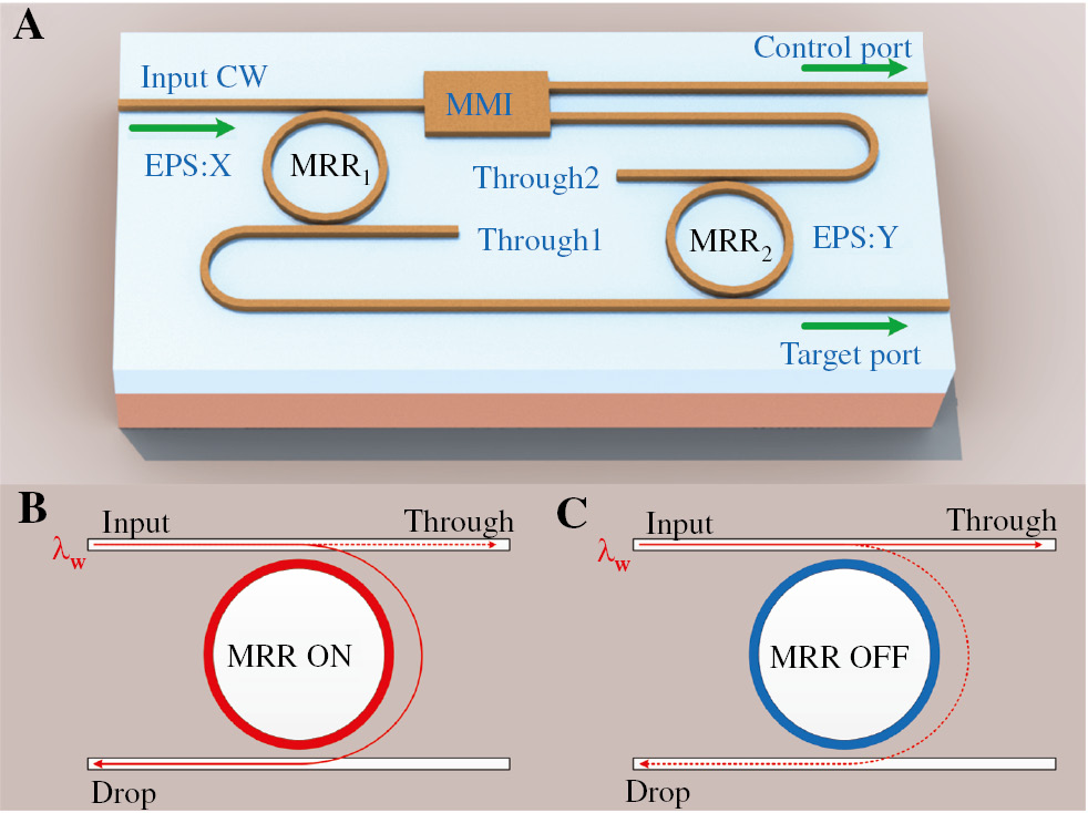
Schematic of the proposed device and switching element. (A) Schematic of the proposed optical Feynman gate (CW, continuous wave; MRR, micro-ring resonator; EPS, electrical pulse sequences; MMI, multimode interference coupler), the control port can implement the function A=X and the target port can implement the function B=X⊕Y. Configurations of MRR-based switching element at (B) ON state and (C) OFF state.
The truth table achieved by the proposed device.
| X | Y | Control port | Target port |
|---|---|---|---|
| 0 | 0 | 0 | 0 |
| 0 | 1 | 0 | 1 |
| 1 | 0 | 1 | 1 |
| 1 | 1 | 1 | 0 |
The working principle of the proposed device can be summarized as follows: a monochromatic continuous optical wave with a working wavelength of λw is coupled into the input port of the device, and the propagation path of the optical wave is controlled by two independent electrical pulse sequences (EPS) X and Y applied on the micro-heaters above MRR1 and MRR2, respectively. The low and high levels of the electrical pulse sequences are defined as logic 0 and 1 in the electrical domain. Meanwhile, the low and high levels of the optical power detected at the Control port and Target port represent logic 0 and logic 1 in the optical domain. We define that each MRR is ON-resonance at λw when the applied voltage is at low level (logic 0), and then the light can be downloaded to the drop port of MRR (Figure 1B). On the contrary, MRR is OFF-resonance when the applied voltage is at high level (logic 1), and then the light is directed to the through port without disturbances (Figure 1C). Based on the working mode definition of MRR, when the voltages applied to MRR1 and MRR2 are both at the low level (X=0, Y=0), the light with the working wavelength of λw coupled into the device is downloaded by MRR1 and MRR2, successively, and the light is directed to the Through2 port at last (Figure 1A). Therefore, the optical power at the Control and Target ports are both at the low level (Control port=0, Target port=0). When the voltages applied to MRR1 and MRR2 are at the low and high levels (X=0, Y=1), respectively, the optical wave is downloaded by MRR1 first, and then bypasses MRR2 directly. The light is directed to the Target port at last. It is obvious that the optical power is at low level at the Control port and high level at the Target port (Control port=0, Target port=1). When the voltages applied to MRR1 and MRR2 are at high and low levels (X=1, Y=0), respectively, the optical wave bypasses MRR1 directly, and then, it is divided into two parts by the MMI coupler. Subsequently, half of the optical wave is directed to the Target port by MRR2, and the remaining optical wave is directed to the Control port simultaneously. Thus, the optical powers are both at the high level at the Control and Target ports (Control port=1, Target port=1). When the voltages applied to MRR1 and MRR2 are both at high levels (X=1, Y=1), the optical wave bypasses MRR1 first, and then, it is divided into two parts by the MMI coupler; after that, half of the optical wave bypasses the MRR2 and propagates to Through2. In the remaining optical wave, half of the light is directed to the Control port simultaneously. The optical power exhibits a low level at the Control port and a high level at the Target port (Control port=1, Target port=0). Based on the above elaboration, the truth table shown in Table 1 can be achieved by the proposed device. From the above discussion, it is clear that the proposed logic circuit can perform the reversible logic operations of two bits, and there is a one-to-one function to identify input signals from their corresponding output signals.
The device is fabricated on a silicon-on-insulator (SOI) wafer with a 220-nm-thick top silicon layer and 2-μm-thick buried SiO2 layer using the commercial CMOS fabrication process. The optical waveguide with 400 nm in width, 220 nm in height, and 90 nm in slab thickness is used to construct the circuit, which only supports the quasi-TE fundamental mode. The radii of MRRs are both 10 μm, all the gaps between ring waveguides and straight waveguides are 400 nm (Figure 2B and C). Spot size converters (SSCs) are integrated on the terminals of the circuit in order to improve the coupling efficiency between the device and input/output lensed fiber (Figure 2A). Two Ω-shaped TiN micro-heaters with widths of 2 μm are fabricated on the top of ring waveguides in order to tune MRRs by thermo-optic effect (Figure 2D). Finally, the aluminum trances are sputtering to connect the TiN micro-heaters and the 80×80 μm2 pads. The microscope image of the fabricated device is shown in Figure 2E.
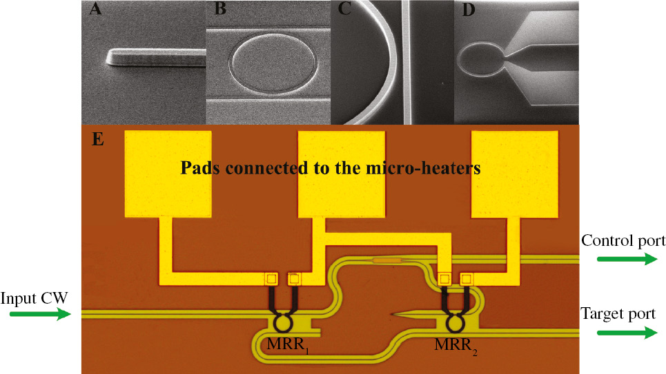
Scanning electronic micrograph (SEM) of (A) the spot size converters (SSC), (B) the parallel MRR, (C) the gap between ring waveguide and straight waveguide, and (D) Ω-shaped TiN micro-heater. (E) Micrograph of the fabricated optical Feynman gate.
An amplified spontaneous emission source (ASE), two tunable voltage sources (TVS), and optical spectrum analyzer (OSA) are first employed to characterize the static response of the device. Meanwhile, the working wavelength and voltages of each electrical pulse sequence are determined by the device’s static characterization. Broadband light generated by ASE is coupled into the input port of the device through a lensed fiber, and the output light is fed into the OSA through another lensed fiber. Two TVSs are employed to tune two TiN micro-heaters above the corresponding MRRs, respectively. The static response spectra at the Control port are shown in Figure 3A–D, and the static response spectra at the Target port are shown in Figure 4A–D.
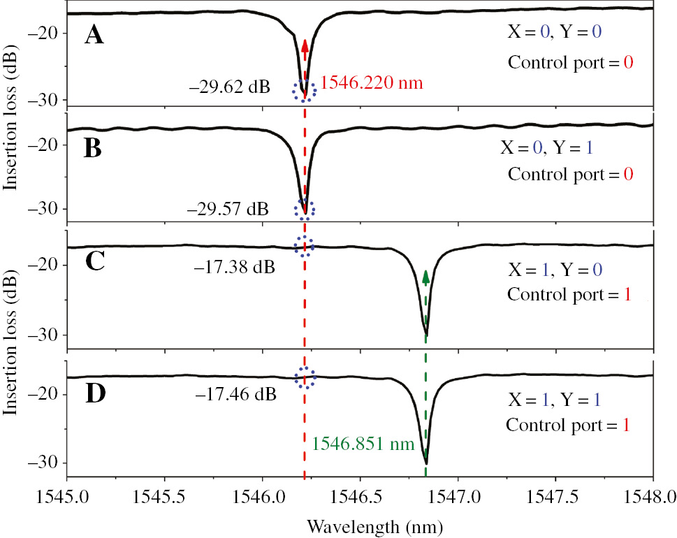
Response spectra of the device at the Control port with the applied voltages to the micro-heaters over MRR1, MRR2, being (A) 0 V and 0.55 V, (B) 0 V and 1.71 V, (C) 1.93 V and 0.55 V, (D) 1.93 V and 1.71 V.
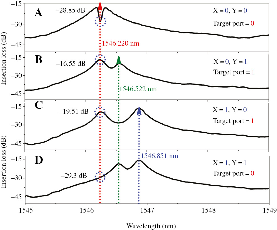
Response spectra of the device at the Target port with the applied voltages to the micro-heaters over MRR1, MRR2, being (A) 0 V and 0.55 V, (B) 0 V and 1.71 V, (C) 1.93 V and 0.55 V, (D) 1.93 V and 1.71 V.
The resonant wavelength of MRR2 is shorter than that of MRR1 due to the limited fabrication accuracy. At first, a pre-bias of 0.55 V is applied to MRR2 to compensate the fabrication error and guarantee that two MRRs have the same resonant wavelength at the original state (X=0, Y=0) (Figure 3A). The wavelength of 1546.22 nm is chosen as the working wavelength.
When the voltages applied to MRR1 and MRR2 through the TiN heaters are 0 V and 0.55 V, respectively (X=0, Y=0), there is a dip at 1546.22 nm due to the identical resonant wavelength of two MRRs. The optical wave is downloaded by MRR1 and MRR2, successively, and directed to the Through2 port at last; therefore, the optical powers at the Control port and Target port are both at a low level (Control port result=0, Target port result=0; Figures 3A and 4A). When the voltages applied to MRR1 and MRR2 are 0 V and 1.71 V (X=0, Y=1), respectively, the MRR2’s resonant wavelength shifts from its original location of 1546.22 nm to 1546.52 nm due to the thermo-optic effect. The optical wave is first downloaded by the MRR1, and then bypassed MRR2, and it is directed to the Target port at last. The optical power is at low level at the Control port and high level at the Target port (Control port result=0, Target port result=1; Figures 3B and 4B). When the voltages applied to MRR1 and MRR2 are 1.93 V and 0.55 V (X=1, Y=0), respectively, the MRR1’s resonant wavelength red-shifts which shift from its original location of 1546.220 nm to 1546.851 nm, due to the thermo-optic effect. The optical wave bypasses MRR1 directly, and then, it is divided into two equal beams by the MMI coupler; afterward, half of the optical wave is downloaded to the Target port by MRR2 and the remaining optical wave is directed to the Control port. Note that logical “1” has two different levels (the high level is about twice the secondary high level) for the device. Comparing Figure 4B with C, the corresponding phenomena also can be observed in the static response spectra (the insertion loss at the working wavelength of 1546.22 nm for Figure 4B is 3 dB higher than that for Figure 4C), but it does not influence the performance of the device as we can define the secondary high level as logical “1”. According to the above discussion, the optical powers at the Control and Target ports are both at a high level in this working status (Control port result=1, Target port result=1; Figures 3C and 4C). When the voltages applied to MRR1 and MRR2 are 1.93 V and 1.71 V (X=1, Y=1), respectively, the optical wave bypasses MRR1 first, and then, it is divided into two equal beams by the MMI coupler; after that, half of the optical wave bypasses MRR2 and propagates to Through2. The remaining optical wave is directed to the Control port simultaneously. The optical power is at high level at the Control port and low level at the Target port (Control port result=1, Target port result=0, Figures 3D and 4D).
The dynamic response results of the device are shown in Figure 5. A continuous monochromatic optical wave at 1546.22 nm from a tunable laser is coupled into the Input port of the device through a lensed fiber. Two independent electrical pulse sequences at 10 kbps are applied to MRR1 and MRR2, respectively (the low levels are 0 V and 0.55 V; the high voltage levels are 1.93 V and 1.71 V for MRR1 and MRR2, respectively). The output optical wave is converted into an electrical signal by a photo-detector (PD). All the two input and output electrical signals are fed into a two-channel oscilloscope for waveform observation. From Figure 5, we can obviously see that the 2-bit reversible logic operation of two electrical signals is achieved at the Control and Target ports, respectively. In addition, the function of the MMI coupler is as a power splitter; therefore, the optical power at the Target port in the working status (“01”) is twice about that at the same port in the working status (“10”). However, it does not influence the performance of the device, and the detailed discussions are given in Ref. [18].
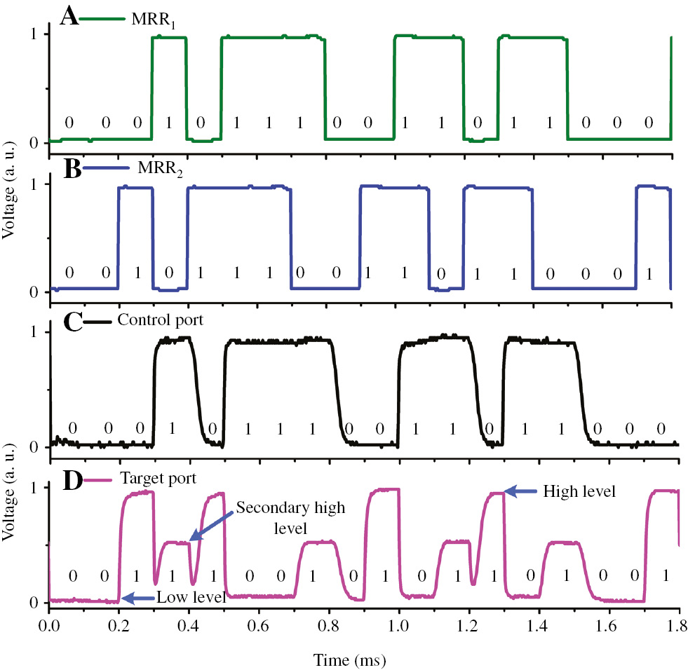
Dynamic experiment results of this device.
(A) Signals applied to MRR1, (B) signals applied to MRR2, (C) operation result of Control port, (D) operation result of Target port.
3 Conclusion
In conclusion, we propose and experimentally demonstrate an optical Feynman gate based on micro-ring resonators for a logically reversible operation with a speed of 10 kbps. There is a one-to-one function to identify inputs from the corresponding outputs, which will be beneficial to construct the “cool” computing. Next, the other advanced modulation schemes, such as the plasma-dispersion effect or the electric field effect can be also employed to tune the MRR-based switch in order to further improve the operation speed of the device [18], [21], [22].
Acknowledgments
This work was supported by the National Science Foundation of China (NSFC) (61405082) and the Fundamental Research Funds for the Central Universities (lzujbky-2016-k05).
Competing interest: The authors declare no competing financial interest.
References
[1] Landauer R. Irreversibility and heat generation in the computing process. IBM J Res Dev 1961;5:183–91.10.1147/rd.53.0183Suche in Google Scholar
[2] Souza CER, Khoury AZ. A Michelson controlled-not gate with a single-lens astigmatic mode converter. Opt Express 2010;18:9207–12.10.1364/OE.18.009207Suche in Google Scholar PubMed
[3] Kostinski N, Fok MP, Prucnal PR. Experimental demonstration of an all-optical fiber-based Fredkin gate. Opt Lett 2009;34:2766–8.10.1364/OL.34.002766Suche in Google Scholar PubMed
[4] Peres A. Reversible logic and quantum computers. Phys Rev A 1985;32:3266.10.1103/PhysRevA.32.3266Suche in Google Scholar PubMed
[5] O’Brien JL, Pryde GJ, White AG, Ralph TC, Branning D. Demonstration of an all-optical quantum controlled-NOT gate. Nature 2003;426:264–7.10.1038/nature02054Suche in Google Scholar PubMed
[6] Nemoto K, Munro WJ. Nearly deterministic linear optical controlled-NOT gate. Phys Rev Lett 2004;93:250502.10.1103/PhysRevLett.93.250502Suche in Google Scholar PubMed
[7] Gao W-B, Xu P, Yao X-C, et al. Experimental realization of a controlled-NOT gate with four-photon six-qubit cluster states. Phys Rev Lett 2010;104:020501.10.1103/PhysRevLett.104.020501Suche in Google Scholar PubMed
[8] Gasparoni S, Pan JW, Walther P, Rudolph T, Zeilinger A. Realization of a photonic controlled-NOT gate sufficient for quantum computation. Phys Rev Lett 2004;93:020504.10.1103/PhysRevLett.93.020504Suche in Google Scholar PubMed
[9] Plantenberg J-H, De Groot PC, Harmans CJPM, Mooij JE. Demonstration of controlled-NOT quantum gates on a pair of superconducting quantum bits. Nature 2007;447:836–9.10.1038/nature05896Suche in Google Scholar PubMed
[10] O’Brien JL, Pryde GJ, Gilchrist A, et al. Quantum process tomography of a controlled-NOT gate. Phys Rev Lett 2004;93:080502.10.1103/PhysRevLett.93.080502Suche in Google Scholar PubMed
[11] Remón P, Ferreira R, Montenegro J-M, Suau R, Pérez-Inestrosa E, Pischel U. Reversible molecular logic: a photophysical example of a Feynman gate. ChemPhysChem 2009;10:2004–7.10.1002/cphc.200900375Suche in Google Scholar PubMed
[12] Zhou C, Wang K, Fan D, et al. An enzyme-free and DNA-based Feynman gate for logically reversible operation. Chem Commun 2015;51:10284–6.10.1039/C5CC02865ESuche in Google Scholar PubMed
[13] Moseley F, Halámek J, Kramer F, Poghossian A, Schöning MJ, Katz E. An enzyme-based reversible CNOT logic gate realized in a flow system. Analyst 2014;139:1839–42.10.1039/c4an00133hSuche in Google Scholar PubMed
[14] Caulfield HJ, Dolev S. Why future supercomputing requires optics. Nat Photo 2010;4:261–3.10.1038/nphoton.2010.94Suche in Google Scholar
[15] Dong P, Chen YK, Duan GH, Neilson DT. Silicon photonic devices and integrated circuits. Nanophotonics 2014;3:215–28.10.1515/nanoph-2013-0023Suche in Google Scholar
[16] Xu Q, Lipson M. All-optical logic based on silicon micro-ring resonators. Opt Express 2007;15:924–9.10.1364/OE.15.000924Suche in Google Scholar PubMed
[17] Qiu C, Ye X, Soref R, Yang L, Xu QF. Demonstration of reconfigurable electro-optical logic with silicon photonic integrated circuits. Opt Lett 2012;37:3942–4.10.1364/OL.37.003942Suche in Google Scholar PubMed
[18] Yang L, Zhang L, Guo C, Ding J. XOR and XNOR operations at 12.5 Gb/s using cascaded carrier-depletion microring resonators. Opt Express 2014;22:2996–3012.10.1364/OE.22.002996Suche in Google Scholar PubMed
[19] Tian Y, Zhang L, Ji R, Yang L, Xu Q. Demonstration of a directed optical encoder using microring-resonator-based optical switches. Opt Lett 2011;36:3795–7.10.1364/OL.36.003795Suche in Google Scholar PubMed
[20] Yang X, Hu X, Yang H, Gong Q. Ultracompact all-optical logic gates based on nonlinear plasmonic nanocavities. Nanophotonics 2017;6:365–76.10.1515/nanoph-2016-0118Suche in Google Scholar
[21] Xu Q, Schmidt B, Pradhan S, Lipson M. Micrometre-scale silicon electro-optic modulator. Nature 2005;435:325–7.10.1038/nature03569Suche in Google Scholar PubMed
[22] Dong P, Liao S, Feng D, et al. Low Vpp, ultralow-energy, compact, high-speed silicon electro-optic modulator. Opt Express 2009;17:22484–90.10.1364/OE.17.022484Suche in Google Scholar PubMed
©2017 Yonghui Tian, Jianhong Yang, et al., published by De Gruyter
This work is licensed under the Creative Commons Attribution-NonCommercial-NoDerivatives 3.0 License.
Artikel in diesem Heft
- Review articles
- Advances in optoplasmonic sensors – combining optical nano/microcavities and photonic crystals with plasmonic nanostructures and nanoparticles
- Periodic array-based substrates for surface-enhanced infrared spectroscopy
- From isolated light-harvesting complexes to the thylakoid membrane: a single-molecule perspective
- Theory and applications of toroidal moments in electrodynamics: their emergence, characteristics, and technological relevance
- Multiple exciton generation in quantum dot-based solar cells
- All-integrated terahertz modulators
- Exciton-plasmon coupling interactions: from principle to applications
- Emerging technologies for high performance infrared detectors
- Research articles
- Magneto-optical response in bimetallic metamaterials
- Saturated evanescent-wave absorption of few-layer graphene-covered side-polished single-mode fiber for all-optical switching
- Reversible thermochromic response based on photonic crystal structure in butterfly wing
- Selection rule engineering of forbidden transitions of a hydrogen atom near a nanogap
- Heterogeneous terahertz quantum cascade lasers exceeding 1.9 THz spectral bandwidth and featuring dual comb operation
- Effect of temperature on the structural, linear, and nonlinear optical properties of MgO-doped graphene oxide nanocomposites
- Engineering light emission of two-dimensional materials in both the weak and strong coupling regimes
- Anisotropic excitation of surface plasmon polaritons on a metal film by a scattering-type scanning near-field microscope with a non-rotationally-symmetric probe tip
- Achieving pattern uniformity in plasmonic lithography by spatial frequency selection
- Controllable all-fiber generation/conversion of circularly polarized orbital angular momentum beams using long period fiber gratings
- High-efficiency/CRI/color stability warm white organic light-emitting diodes by incorporating ultrathin phosphorescence layers in a blue fluorescence layer
- Relative merits of phononics vs. plasmonics: the energy balance approach
- Efficiency enhancement of InGaN amber MQWs using nanopillar structures
- Color display and encryption with a plasmonic polarizing metamirror
- Experimental demonstration of an optical Feynman gate for reversible logic operation using silicon micro-ring resonators
- Specialized directional beaming through a metalens and a typical application
- Anomalous extinction in index-matched terahertz nanogaps