
High-efficiency/CRI/color stability warm white organic light-emitting diodes by incorporating ultrathin phosphorescence layers in a blue fluorescence layer
-
Yanqin Miao
 ,
Kexiang Wang
,
Kexiang Wang

Abstract
By incorporating ultrathin (<0.1 nm) green, yellow, and red phosphorescence layers with different sequence arrangements in a blue fluorescence layer, four unique and simplified fluorescence/phosphorescence (F/P) hybrid, white organic light-emitting diodes (WOLEDs) were obtained. All four devices realize good warm white light emission, with high color rending index (CRI) of >80, low correlated color temperature of <3600 K, and high color stability at a wide voltage range of 5 V–9 V. These hybrid WOLEDs also reveal high forward-viewing external quantum efficiencies (EQE) of 17.82%–19.34%, which are close to the theoretical value of 20%, indicating an almost complete exciton harvesting. In addition, the electroluminescence spectra of the hybrid WOLEDs can be easily improved by only changing the incorporating sequence of the ultrathin phosphorescence layers without device efficiency loss. For example, the hybrid WOLED with an incorporation sequence of ultrathin red/yellow/green phosphorescence layers exhibits an ultra-high CRI of 96 and a high EQE of 19.34%. To the best of our knowledge, this is the first WOLED with good tradeoff among device efficiency, CRI, and color stability. The introduction of ultrathin (<0.1 nm) phosphorescence layers can also greatly reduce the consumption of phosphorescent emitters as well as simplify device structures and fabrication process, thus leading to low cost. Such a finding is very meaningful for the potential commercialization of hybrid WOLEDs.
1 Introduction
White organic light-emitting diodes (WOLEDs) have been widely studied in the past decades for their potential utilization in flat-panel displays and solid-state lighting, mainly due to their advantages, such as their high efficiency, transparency, flexibility, and exceptional light-weight, ultra-thin characteristics, to name a few [1], [2], [3], [4]. In order to achieve high device efficiency, phosphorescent materials have been widely used to fabricate such devices because they allow manufacturers to harvest 25% singlet excitons and 75% triplet excitons, thus achieving internal quantum efficiency of 100%, compared with the 25% theoretical value for fluorescent materials [3], [4], [5], [6], [7], [8]. However, the all-phosphorescent WOLEDs are limited by i) the absence of efficient blue phosphors with long operational lifetimes that are suitable for commercial applications [9], [10], and ii) the difficulty of conducting carrier injection from an adjacent carrier transporting layer to the large-bandgap host material with higher triplet state energy [11]. Thus, one promising approach to achieve WOLEDs with high efficiency and long lifetime is to combine emissions from blue fluorophores and long wavelength phosphors, also called fluorescence/phosphorescence (F/P)-based hybrid WOLEDs. They are ideal options because of their unique advantage of combining the excellent stability of blue fluorophores and the high efficiency of long wavelength phosphors [1], [11], [12], [13], [14].
In the past years, enormous efforts have been exerted to simultaneously harvest both the singlet and triplet excitons and obtain high-performance hybrid WOLEDs. Towards this end, a series of novel device structures for hybrid WOLEDs have been reported. For hybrid WOLEDs, two types of dominant device architectures have been proposed: the single-emissive layer (single-EML) structure [11], [13], [15], [16], [17], [18] and the multi-emissive layer (multi-EML) structure [1], [10], [11], [14], [19], [20]. In order to obtain ideal white emission in single-EML hybrid WOLEDs, the doping concentration of phosphors in the blue fluorophore host must be precisely controlled. This must be done in order to suppress the transfer of singlet excitons from the blue fluorophore to the phosphors via Förster energy transfer [10], [11], [12], [15], thus inducing a complicated device preparation process. In the multi-EML hybrid WOLEDs, for harvesting complete electrically generated excitons, a commonly used configuration is to incorporate an interlayer between the fluorescent and the phosphorescent dopant layers, which separates the singlet and triplet excitons to their individual emitting zones [1], [11], [15], [21], [22]. However, this can create a complicated device structure that involves a complicated device preparation process; in turn, this leads to high fabrication cost and poor reproducibility for devices, which is not conducive to industrial mass production.
To ensure the success of WOLED technology as a major industry capable of competing with conventional lighting and display technologies, there exists a need to develop novel hybrid WOLEDs with simplified device structures and fabrication processes while achieving low cost and high productivity. By doping a blue fluorophore into mixed hosts containing hole- and electron-transporting materials, Ma et al. [21] developed a series of novel hybrid WOLEDs without using an interlayer, showing external quantum efficiencies (EQE) ranging from 16.5%–19.0%. The device structure of hybrid WOLEDs is effectively simplified, but these hybrid WOLEDs still involve a complicated device preparation process for a precise control of doping concentration. In another study, Ma et al. [23] inserted an ultra-thin red phosphorescent EML into a blue-emitting electron transport layer (ETL) and an ultra-thin green phosphorescent EML into the hole transport layer (HTL) to develop a doping-free hybrid WOLED. The device structure of the hybrid WOLEDs is very simple, but they achieved a relatively low device efficiency (23.2 cd/A at 1000 cd/m2). Recently, Cao et al. [24] reported simplified but high-performance hybrid WOLEDs with ultrathin (<1 nm) emitting nanolayers, which were also fabricated by using a doping-free process. The simplified device structure and doping-free process can help shorten the fabrication process and improve the reproducibility; moreover, the use of ultrathin (<1 nm) emitting nanolayers can effectively reduce cost. However, an ultra-high color rending index (CRI) of 91.3 was obtained only at a low luminance of 10 cd/m2, and device efficiency for proposed hybrid WOLED was relatively low (with a power efficiency of 14.6 lm/W). Furthermore, several interlayers were still required during device fabrication. In fact, the excellent device stability and high CRI for WOLEDs are also key factors that are as important as other parameters, such as high efficiency, high brightness, and low cost [3], [8], [12], [18], [25], [26]. Although some reported hybrid WOLEDs have realized high efficiency, problems still exist, including poor color stability and low CRI [10], [15]. Especially, for a simplified hybrid WOLED, simultaneously realizing high efficiency, ultra-high CRI, and good color stability remains a big challenge.
In the current work, bis[2-(2-hydroxyphenyl)-pyridine]beryllium(Bepp2), possessing a high fluorescent quantum yield of >0.80 [27] and a high triplet energy level (2.6 eV) [28], was selected as an efficient blue fluorophor. By incorporating a set of different sequentially arranged ultrathin (<0.1 nm) green, yellow, and red phosphorescence layers into a Bepp2 layer, the four unique hybrid WOLEDs were demonstrated. The four hybrid WOLEDs all achieve high CRI of >80, low correlated color temperature (CCT) of <3600 K, and high color stability at a wide voltage range of 5 V–9 V. Moreover, all hybrid WOLEDs reveal high forward-viewing EQEs of 17.82%–19.34%. Especially, the hybrid WOLED with ultrathin red/yellow/green sequence incorporation exhibits an ultra-high CRI of 96 and a high EQE of 19.34%.
2 Materials and methods
2.1 Materials information
In this work, phosphor (bis(2-(3-trifluoromethyl-4-fluorophenyl)-4-methylquinolyl) (acetylacetonate)iridium(III) (Ir(ffpmq)2(acac)) was synthesized in our laboratory. Other active materials used for device fabrication were obtained from Nichem Fine Technology Co. Ltd, Taiwan and used without further purification. The chemical structures of all organic materials involved in blue and white devices in this work are shown in Figure S1.
2.2 Device fabrication
The devices were fabricated on pre-patterned indium tin oxide (ITO) glass substrates with a sheet resistance of 15 Ω/square. The ITO glass substrates were cleaned sequentially by using detergent, acetone, isopropyl alcohol, and deionized water before use. Prior to the thin-film deposition, the substrates were treated with UV ozone to improve the work function. Afterwards, the ITO glass substrates were loaded into a vacuum chamber for organic layer deposition by thermal evaporation under a base pressure of 5×10⁻⁴ Pa. The film thickness and deposition rates of the function materials were monitored by a calibrated crystal quartz sensor. Deposition rates for organic layers, LiF, and Al, were controlled at about 1 Å/s, 0.1 Å/s, and 3 Å/s–6 Å/s, respectively. The overlap between ITO anode and Al cathode was 3 mm ×3 mm, as the active emissive area of the devices.
2.3 Device characterization
The electroluminescence (EL) spectra, Commission Internationale de L’Eclairage (CIE) coordinates, CRI, and CCT of OLEDs were measured by using a computer-controlled PR-655 (Photo Research) spectra scan spectrometer. The current-voltage-luminance (J-V-L) characteristics were measured by a computer-controlled Keithley 2400 source meter integrated with a BM-7A luminance meter test system purchased from Fstar Scientific Instrument, China. Current efficiency (CE) and power efficiency (PE) were calculated from the plot of J-V-L. The EQE is calculated by using the formula [29]
where L (cd/m2) is the total luminance of device, J (mA/cm2) is the density of the current flowing into the EL device, λ (nm) is the EL wavelength, I(λ) is the relative EL intensity at each wavelength and obtained by measuring the EL spectrum, K(λ) is the CIE standard photopic efficiency function, e is the charge of an electron, h is Planck’s constant, and c is the velocity of light. Here, the EL spectrum data, used to calculate EQE, were measured at an operating voltage of 6 V.
All samples were characterized immediately after thin-film deposition without encapsulation.
3 Results and discussion
3.1 A suitable blue fluorophor and blu-based device
To develop efficient, high-quality hybrid WOLEDs, a suitable blue fluorophor with pure blue emission and high fluorescent quantum yield is a prerequisite. In addition, if the blue fluorophor possesses a high triplet energy level, this is beneficial for simplifying device structure, and realizing high device efficiency as they facilitate the complete harvesting electrically generated excitons [13], [30]. Here, Bepp2, showing a high fluorescent quantum yield of 80% and a high triplet energy of 2.6 eV [27], [28], was selected as a candidate of such ideal blue fluorophors.
To demonstrate the viability of Bepp2 for high-performance hybrid WOLEDs, a series of Bepp2-based blue OLEDs with different Bepp2 layer thicknesses were fabricated. The structure of the blue OLEDs is as follows: ITO/MoO3 (3 nm)/ TCTA (40 nm)/Bepp2 (x nm)/TPBi (50 nm)/LiF (1 nm)/Al (200 nm), where, x can be 5, 7, 10, and 12, corresponding to the B1, B2, B3, and B4 devices, respectively. In these devices, Bepp2 served as blue fluorescent emitter, 4,4′,4′′-tris(N-carbazolyl)triphenylamine (TCTA) served as the HTL and electron-blocking layer (EBL), and 1,3,5-tris(phenyl-2-benzimidazolyl)benzene (TPBi) served as the ETL and hole-blocking layer (HBL). MoO3, LiF, and Al were used as the hole injection layer (HIL), electron injection layer (EIL), and cathode, respectively. The chemical structures of all organic materials involved in the blue devices and latter white devices are shown in Figure S1.
Figure 1A shows the luminance-voltage (L-V) characteristic curves of Bepp2-based blue OLEDs. As can be seen, when the thickness of the Bepp2 layer increase from 5 nm, 7 nm, to 10 nm, the maximum luminance for the corresponding devices B1, B2, and B3 improve rapidly, from 3463 cd/m2, 4380 cd/m2, to 5565 cd/m2, respectively. However, when the thickness of the Bepp2 layer further increases from 10 nm to 12 nm, the corresponding device B4 only shows a slightly improved maximum luminance, reaching 5838 cd/m2. Thus, the optimum thickness for Bepp2 layer for developing efficient high-quality white OLEDs is confirmed to be 10 nm. Figure 1B exhibits the normalized EL spectra of device B3 with 10 nm-thick Bepp2 layer at different voltages, and the inset is a picture for device B3 at 6 V. As can be seen, the device B3 exhibits a pure deepblue emission with a peak at 440 nm and CIE values (0.158, 0.110) at 6 V. The EL spectra show high stability with an insignificant change when the voltage increases from 5 V to 10 V, suggesting that large gaps and high triplet energy levels of TCTA (3.4 eV and 2.8 eV) [31] and TPBi (4.0 eV and 2.7 eV) [12], [32] can strictly confine the generated excitons in the EML, which is helpful in fabricating high-performance WOLEDs.
(A) L–V characteristic curves of Bepp2-based blue devices; (B) Normalized EL spectra of device B3 at different voltages, Inset: A picture for device B3 at 6 V.
3.2 Complementary phosphors for developing white devices
Further, for demonstrating high-quality WOLEDs, adequate complementary emitters are essential [3]. Here, phosphorescent tris(2-phenylpyridine)iridium(III)) (Ir(ppy)3), Ir(ffpmq)2(acac), and bis(1-phenylisoquinoline)(acetylacetonate)iridium(III) (Ir(piq)2(acac)) were employed for green, yellow, and red emissions, respectively. The EL spectra of the three emitters were investigated from a common device with the structure of ITO/ N,N′-bis(naphthalen-1-yl) -N,N′-bis(phenyl)-benzidine (NPB)(40 nm)/ 4,4′-N,N′-dicarbazolylbiphenyl (CBP): 6 wt% emitter (30 nm)/ TPBi(35 nm)/ LiF(1 nm)/ Al(200 nm), in which the emitters were Ir(ppy)3, Ir(ffpmq)2(acac), and Ir(piq)2(acac), respectively. Along with the EL spectrum for device B3 at 6 V, the normalized EL spectra of the four emitters are displayed in Figure 2. As can be seen, the monochromatic EL spectra of the four emitters cover most of the visible region, suggesting the probability of employing all four emitters to obtain high-quality WOLEDs.
Normalized monochromatic EL spectra of four emitters Bepp2, Ir(ppy)3, Ir(ffpmq)2(acac), and Ir(piq)2(acac).
3.3 Proposed WOLEDs and the basic principle
On the basis of the above conclusions, by combining fluorescent Bepp2 with phosphorescent Ir(ppy)3, Ir(ffpmq)2(acac), and Ir(piq)2(acac), four unique simplified four-color hybrid WOLEDs were fabricated by incorporating ultrathin Ir(ppy)3, Ir(ffpmq)2(acac), and Ir(piq)2(acac) layers (<0.1 nm) with different sequential arrangements into a Bepp2 layer, as shown in Figure 3. These devices were named as device W1 for the incorporation with red/yellow/green sequence, device W2 for the incorporation with green/yellow/red sequence, device W3 for the incorporation with green/red/yellow sequence, and device W4 for the incorporation with yellow/red/green sequence. The detailed device structures are listed below:
Device structure diagram of the proposed hybrid white devices W1, W2, W3, and W4.
Device W1: ITO/MoO3 (3 nm)/TCTA (40 nm)/Bepp2 (3 nm)/Ir(piq)2(acac) (0.08 nm)/Bepp2 (2 nm)/Ir(ffpmq)2(acac) (0.06 nm)/Bepp2 (2 nm)/Ir(ppy)3 (0.03 nm)/Bepp2 (3 nm)/TPBi (50 nm)/LiF (1 nm)/Al (200 nm)
Device W2: ITO/MoO3 (3 nm)/TCTA (40 nm)/Bepp2 (3 nm)/Ir(ppy)3 (0.03 nm)/Bepp2 (2 nm)/Ir(ffpmq)2(acac) (0.06 nm)/Bepp2 (2 nm)/Ir(piq)2(acac) (0.08 nm)/Bepp2 (3 nm)/TPBi (50 nm)/LiF (1 nm)/Al (200 nm)
Device W3: ITO/MoO3 (3 nm)/TCTA (40 nm)/Bepp2 (3 nm)/Ir(ppy)3 (0.03 nm)/Bepp2 (2 nm)/Ir(piq)2(acac) (0.08 nm)/Bepp2 (2 nm)/Ir(ffpmq)2(acac) (0.06 nm)/Bepp2 (3 nm)/TPBi (50 nm)/LiF (1 nm)/Al (200 nm)
Device W4: ITO/MoO3 (3 nm)/TCTA (40 nm)/Bepp2 (3 nm)/Ir(ffpmq)2(acac) (0.06 nm)/Bepp2 (2 nm)/Ir(piq)2(acac) (0.08 nm)/Bepp2 (2 nm)/Ir(ppy)3 (0.03 nm)/Bepp2 (3 nm)/TPBi (50 nm)/LiF (1 nm)/A l(200 nm)
Here, ultrathin sheets of phosphors with a thickness of <0.1 nm do not form a neat layer but partially penetrate into the adjacent Bepp2 [33], [34]; hence, they serve as dopants in adjacent Bepp2. In addition, in these white devices, different-color ultrathin phosphorescence layers are incorporated away from HTL/EML and EML/ETL interfaces for 3 nm, and they are also separated by a 2 nm-thick Bepp2 layer. This is because the carrier recombination zone in these WOLEDs should be mainlylocated at the TCTA/EML interface and partially at the EML/ETL interface and whole EML due to the following reasons: i) TCTA and TPBi mostly conduct holes and electrons, respectively; ii) the high energy barriers of 0.3 eV and 0.6 eV at the TCTA/Bepp2 and Bepp2/TPBi interfaces (see Figure 5); and iii) a high electron mobility of ~10−4 cm2/Vs for Bepp2 [28], [30], respectively. The generated singlet excitons at the HTL/EML and EML/ETL interfaces can be directly recombined on Bepp2 for blue emission because of a short Förster energy transfer radius of about 3 nm [1], [13], [15], [24], which does not allow singlet excitons to transfer energy to ultrathin phosphorescent layers for phosphorescent emission. Furthermore, the generated triplet excitons at the HTL/EML and EML/ETL interfaces can migrate to ultrathin phosphorescent layers at the middle of EML for different color phosphorescent emissions owing to a long diffusion distance of >10 nm for triplet excitons [3], [13]. For balancing emission intensity of different color, a 2 nm-thick Bepp2 layer between two different-color ultrathin phosphorescent layers is used to partially block energy transfer from high triplet excitons to low triplet excitons. This is because of a higher triplet level (2.6 eV) for Bepp2 [28] than those (<2.4 eV) for phosphorescent emitters (see Figure 5). Thus, in theory, all the electrically generated singlet and triplet excitons in these devices can be effectively utilized for radiative decay, realizing 100% exciton utilization efficiency. Moreover, the emission intensity for different colors can bewell balanced by the management of singlet and triplet excitons, and as such, they are expected to realize efficient and high-quality white emission.
Figure 4 shows the EL spectra of four white devices W1, W2, W3, W4 at different driving voltages, as well as the corresponding CIE coordinates, CCT, and CRI. As expected, all hybrid WOLEDs realize good warm white emission and the EL spectra for four devices all contain four main emission peaks at about 452 nm, 508 nm, 552 nm, and 620 nm, which come from Bepp2, Ir(ppy)3, Ir(ffpmq)2(acac), and Ir(piq)2(acac), respectively. These values indicate that the generated singlet and triplet excitons are managed well for the emission of individual color. Furthermore, all hybrid WOLEDs reveal high CRI of >80 with relatively low CCT of <3600 K at a wide voltage range of 5 V–9 V due to a dominant red light emission peak in EL spectra. However, a big distinction exists in EL spectra for four hybrid WOLEDs, which can be attributed to the different sequential arrangements of incorporating ultrathin Ir(ppy)3 (0.03 nm), Ir(ffpmq)2(acac) (0.06 nm), and Ir(piq)2(acac) (0.08 nm) layers into a Bepp2 layer.
EL spectra, CIE coordinates, CCT, and CRI of all four white devices at different driving voltages.
Note: the luminances for four white devices are listed at different driving voltages, (A) for device W1, (B) for device W2, (C) for device W3, (D) for device W4.
Figure 5 displays the schematic diagrams of the emission mechanisms of four white devices, (A) for device W1, (B) for device W2, (C) for device W3, and (D) for device W4. For device W1, because the ultrathin layer of Ir(piq)2(acac) with lowest triplet level is close to the main carrier recombination zone (TCTA/Bepp2 interface), the triplet excitons generated at the TCTA/Bepp2 interface can migrate easily to the ultrathin Ir(piq)2(acac) layer and transfer energy to Ir(piq)2(acac) for red emission. In addition, although the triplet level of Bepp2 (2.6 eV) is higher than those of Ir(ppy)3 (2.4 eV) and Ir(ffpmq)2(acac) (2.2 eV), a portion of triplet excitons in ultrathin Ir(ppy)3 and Ir(ffpmq)2(acac) layers can still penetrate the 2 nm-thick Bepp2 layer and diffuse to the ultrathin Ir(piq)2(acac) layer for red emission because i) the 2 nm Bepp2 layer is relatively thin, and ii) due to the lowest triplet level for Ir(piq)2(acac)(2.0 eV), which contributes to a warm white emission with a highcolor quality. For example, the EL spectra of device W1 exhibits a stepincreasing emission intensity from blue, green, yellow, to red, which is similar to the spectra of light emitted by incandescent light bulbs. Accordingly, device W1 achieved an ultra-high CRI of 95–96 and a low CCT of 2353 K–2559 K at a wide voltage range of 5 V–9 V. To the best of our knowledge, this is the first study to introduce a hybrid WOLED with ultrathin EMLs showing such a high CRI of 96 [24], [35]. On the contrary, in device W2, the location of ultrathin Ir(piq)2(acac) layer is away from the TCTA/Bepp2 interface by about 7 nm. In this case, the triplet excitons generated at TCTA/Bepp2 interface will be first consumed by Ir(ppy)3 for green emission, then transfer energy to Ir(ffpmq)2(acac) for yellow emission, while the remaining triplet excitons migrate to the Ir(piq)2(acac) layer for red emission, leading to an increased green and yellow emissions compared with those in device W1. As a consequence, device W2 shows a reduced CRI of 83–85 and a relatively high CCT of 3335 K–3579 K at a wide voltage range of 5 V–9 V.
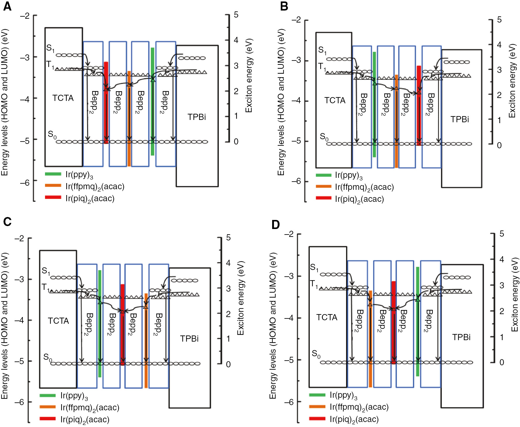
Schematic diagrams of the emission mechanisms of four white devices.
(A) For device W1, (B) for device W2, (C) for device W3, (D) for device W4. The circles and triangles are the exciton energies (S1, S0, and T1).
In devices W3 and W4, the ultrathin Ir(piq)2(acac) layer is located at thein between middle of the ultrathin Ir(ppy)2 and Ir(ffpmq)2(acac) layers. A portion of the triplet excitons generated at the TCTA/Bepp2 and Bepp2/TPBi interfaces can be firstly utilized by the ultrathin green and yellow layers, and the remaining triplet excitons also willcan also penetrate 2 nm-thick Bepp2 layer to transfer energy to the ultrathin Ir(piq)2(acac) layer, thus realizing white emission. The different green and yellow intensitiesy in the EL spectra for devices W3 and W4 should be ascribed to the perversion of position for the ultrathin Ir(ppy)2 and Ir(ffpmq)2(acac) layers incorporated into a blue fluorescence layer. The difference in EL spectra also leads to different color qualities. For example, as a result of a reduced green emission intensity in EL spectra, device W3 reveals a high CRI of 86–90 and a low CCT of 2505 K–2789 K at a wide voltage range of 5 V–9 V, whereas device W4 shows a relatively low CRI of 81–85 and a lowest CCT of 2094 K–2190 K at a wide voltage range of 5 V–9 V.
In addition, all hybrid WOLEDs also reveal high color stability with a slight EL spectra change at a wide voltage range from 5 V–9 V, which can be attributed to i) a strictly limited carrier recombination zone due to a high energy barriers of 0.3 eV and 0.6 eV at TCTA/Bepp2 and Bepp2/TPBi interfaces, respectively, and ii) the energy transfer rate from the high-energy level triplet excitons to the low-energy level triplet excitons remain constant at a wide voltage range due to a thicker red phosphorescence ultrathin layer.
Meanwhile, Figure 6 shows the current efficiency–luminance–EQE (CE–L–EQE) curves of the four hybrid WOLEDs, and the insert is the J–V–L curves of the individual white devices. Some EL performance parameters are summarized in Figure 4 and Table 1. As we can see, all these devices show the same turn on voltage of 3.3 V due to the approximately similar device structures of the four hybrid WOLEDs. The maximum luminance related to EL spectra of the white devices, reaches 47,470 cd/m2 for device W1, 52,870 cd/m2 for device W2, 51,780 cd/m2 for device W3, and 42,070 cd/m2 for device W4, dependent on the different radiation intensities for four different color emitters. The maximum CE and PE are 32.19 cd/A and 30.65 lm/W for device W1, 40.65 cd/A and 34.25 lm/W for device W2, 30.21 cd/A and 25.34 lm/W for device W3, and 31.01 cd/A and 28.27 lm/W for device W4, respectively. Although the CE and PE for the four white devices show big differences, the maximum EQEs of these devices are similar, ranging from 17.82%–19.34% (19.34% for device W1, 18.40% for device W2, 18.82% for device W3, and 17.82% for device W4). These results indicate that, despite the different sequence incorporations for ultrathin green, yellow, and red phosphorescence layers in a blue fluorescence layer, all hybrid WOLEDs allow almost complete electrically generated exciton harvesting for light emission. Meanwhile, some slight differences in EQEs, such as higher EQE for device W1, is ascribed to the ultrathin Ir(piq)2(acac) layer of the lowest triplet level close to the main carrier recombination zone (TCTA/Bepp2 interface), but there exists a slight energy loss for triplet excitons from energy transfer from the high triplet level emitter to the low triplet level emitter in the three other hybrid WOLEDs.
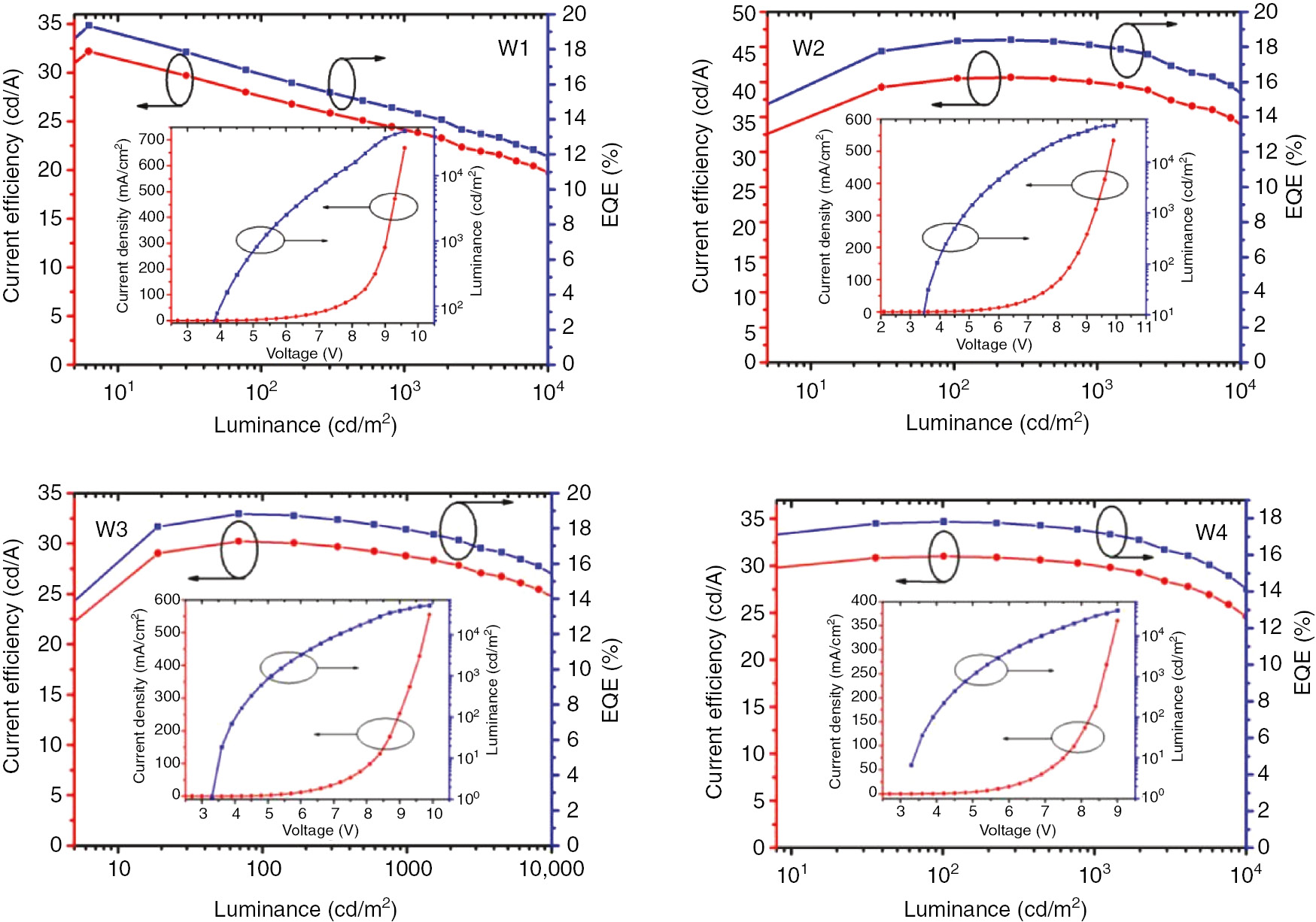
CE–L–EQE characteristic curves for four white devices, Inset: J-V-L characteristic curve for the corresponding white device.
Summary of the performances of the four WOLEDs.
| Devices | Von (V)a | Maximum | CIE (x, y) @5 V–9 V | CCT (K) @5 V–9 V | CRI @5/6/7/8/9 V | ||
|---|---|---|---|---|---|---|---|
| EQE (%) | CE (cd/A) | PE (lm/W) | |||||
| W1 | 3.3 | 19.34 | 32.19 | 30.65 | (0.504, 0.436)–(0.482, 0.430) | 2353–2559 | 95/96/96/96/96 |
| W2 | 3.3 | 18.40 | 40.65 | 34.25 | (0.448, 0.476)–(0.427, 0.462) | 3335–3579 | 84/83/83/84/85 |
| W3 | 3.3 | 18.82 | 30.21 | 25.34 | (0.490, 0.435)–(0.464, 0.430) | 25052789 | 86/86/86/88/90 |
| W4 | 3.3 | 17.82 | 31.01 | 28.27 | (0.525, 0.427)–(0.505, 0.412) | 20942190 | 81/80/81/82/85 |
aTurn-on voltage estimated at a brightness of >1 cd/m2.
The proposed hybrid WOLEDs show unique and simplified device structures, which are beneficial for reducing fabrication cost and improving the reproducibility of the devices. Moreover, the hybrid WOLEDs with ultrathin phosphorescence layers (<0.1 nm) can largely reduce the use of phosphorescent emitters, further reducing the cost of WOLEDs. It is worth noting that the EL spectra of hybrid WOLEDs can be easily improved by simply changing the incorporation sequence of the ultrathin phosphorescence layers into a blue fluorescence layer for obtaining ideal white emission. For example, the hybrid WOLEDs with ultrathin red/yellow/green sequence incorporations show ultra-high CRI values of 95–96. Combining a high EQE of 19.34% and color stability, to our knowledge, this is also the first WOLED with good tradeoff among device efficiency, CRI, and color stability [1], [13], [14], [17], [18], [21], [22], [23], [24], [35], [36], [37], [38], [39], [40]. Such findings can provide an effective way to achieve low-cost, high-efficiency/CRI/color stability WOLEDs with unique and simplified structures for a wide range of next-generation lighting applications.
4 Conclusion
In this work, Bepp2, possessing a high fluorescent quantum yield of >0.80 and a high triplet energy level (2.6 eV), was selected as an efficient blue fluorophor. By incorporating ultrathin (<0.1 nm) green, yellow, and red phosphorescence layers with different sequential arrangements into a Bepp2 layer, four unique simplified hybrid WOLEDs were achieved. All four hybrid WOLEDs all realize good warm white emission, showing high CRI of >80 and high color stability under a wide voltage range from 5 V–9 V. These hybrid WOLEDs also reveal high forward-viewing EQE of 17.82%–19.34%, indicating an almost complete harvesting of electrically generated excitons. Specifically, the hybrid WOLED with ultrathin red/yellow/green sequence incorporation exhibits an ultra-high CRI of 96 and a high EQE of 19.34% simultaneously. To the best of our knowledge, this is the first WOLED with good tradeoff among device efficiency, CRI, and color stability. These results indicate that the proposed novel architecture would be an effective way to develop low-cost, high-efficiency/CRI/color stability WOLEDs with unique and simplified structures for a wide range of next-generation lighting applications.
5 Supplementary material
The supporting data/information will be available online on the journal’s website
Acknowledgment
This work was supported by K.C. Wong Education Foundation – Hong Kong Baptist University (HKBU) Fellowship Programme for Mainland Visiting Scholars 2016-17, Program for New Century Excellent Talents of the University of Ministry of Education of China (NCET-13-0927), National Natural Science Foundation of China (Grant Nos. 61307030 and 61307029), Shanxi Provincial Key Innovative Research Team in Science and Technology (Grant Nos. 201513002-10 and 201605D131045-10), Natural Science Foundation for Shanxi Province (Grant Nos. 201601D021018, 2015021070, 2015021028, and 201601D011031), Shanxi University Scientific and Technical Innovation Project (Grant Nos. 2016135 and 2015177), HKBU Inter-institutional Collaborative Research Scheme (ICRS) (Project No. RC-ICRS/15-16/04) and Shenzhen Peacock Plan (KQTD20140630110339343).
References
[1] Sun Y, Giebink NC, Kanno H, Ma B, Thompson ME, Forrest SR. Management of singlet and triplet excitons for efficient white organic light-emitting devices. Nature 2006;440: 908–12.10.1038/nature04645Suche in Google Scholar PubMed
[2] Wang JX, Chen JS, Qiao XF, Alshehri SM, Ahamad T, Ma DG. Simple-structured phosphorescent warm white organic light-emitting diodes with high power efficiency and low efficiency roll off. ACS Appl Mater Interfaces 2016;8:10093–7.10.1021/acsami.6b00861Suche in Google Scholar PubMed
[3] Miao YQ, Gao ZX, Wang H, et al. Extremely high chromatic-stability white organic light-emitting device with symmetrical cascade emissive layer. Org Electron 2015;23:199–207.10.1016/j.orgel.2015.05.006Suche in Google Scholar
[4] Chang YL, Song Y, Wang ZB, et al. Highly efficient warm white organic light-emitting diodes by triplet exciton conversion. Adv Funct Mater 2013;23:705–12.10.1002/adfm.201201858Suche in Google Scholar
[5] Zhu LP, Wu ZB, Chen JS, Ma DG. Reduced efficiency roll-off in all-phosphorescent white organic light-emitting diodes with an external quantum efficiency of over 20%. J Mater Chem C 2015;3:3304–10.10.1039/C5TC00205BSuche in Google Scholar
[6] Udagawa K, Sasabe H, Cai C, Kido J. Low-driving-voltage blue phosphorescent organic light-emitting devices with external quantum efficiency of 30%. Adv Mater 2014;26:5062–6.10.1002/adma.201401621Suche in Google Scholar PubMed
[7] Seo JH, Lee SJ, Seo BM, et al. White organic light-emitting diodes showing nearly 100% internal quantum efficiency. Org Electron 2010;11:1759–66.10.1016/j.orgel.2010.07.015Suche in Google Scholar
[8] Miao YQ, Gao ZX, Li YH, et al. Multiple emissive layers white organic light emitting device with nanoplatforms patterning structure for improved current efficiency and color balance. Synth Met 2015;203:59–67.10.1016/j.synthmet.2015.02.017Suche in Google Scholar
[9] Su SJ, Gonmori E, Sasabe H, Kido J. Highly efficient organic blue-and white-light -emitting devices having a carrier- and exciton-confining structure for reduced efficiency roll-Off. Adv Mater 2008;20:41–4194.10.1002/adma.200801375Suche in Google Scholar
[10] Wu ZB, Luo JJ, Sun N, et al. High-performance hybrid white organic light-emitting diodes with superior efficiency/color rendering index/color stability and low efficiency roll-off based on a blue thermally activated delayed fluorescent emitter. Adv Funct Mater 2016;26:3306–13.10.1002/adfm.201505602Suche in Google Scholar
[11] Ye J, Zheng CJ, Ou XM, Zhang XH, Fung MK, Lee CS. Management of singlet and triplet excitons in a single emission layer: a simple approach for a high-efficiency fluorescence/phosphorescence hybrid white organic light-emitting device. Adv Mater 2012;24:3410–4.10.1002/adma.201201124Suche in Google Scholar PubMed
[12] Miao YQ, Zhao B, Gao ZX, et al. A novel intramolecular charge transfer blue fluorophor for high color stability hybrid di-chromatic white organic light-emitting diodes. Org Electron 2017;42:1–7.10.1016/j.orgel.2016.12.016Suche in Google Scholar
[13] Schwartz G, Reineke S, Rosenow TC, Walzer K, Leo K. Triplet harvesting in hybrid white organic light-emitting diodes. Adv Funct Mater 2009;19:1319–33.10.1002/adfm.200801503Suche in Google Scholar
[14] Sun N, Wang Q, Zhao YB, et al. A hybrid white organic light-emitting diode with above 20% external quantum efficiency and extremely low efficiency roll-off. J Mater Chem C 2014;2:7494–504.10.1039/C4TC01149JSuche in Google Scholar
[15] Wu ZB, Ma DG. Recent advances in white organic light-emitting diodes. Mat Sci Eng R 2016;107:1–42.10.1016/j.mser.2016.06.001Suche in Google Scholar
[16] Kido J. Hongawa K, Okuyama K, Nagai K. White light-emitting organic electroluminescent devices using the poly(N-vinylcarbazole) emitter layer doped with three fluorescent dyes. Appt Phys Lett 1994;7:815–7.10.1063/1.111023Suche in Google Scholar
[17] Chen YH, Zhao FC, Zhao YB, Chen JS, Ma DG. Ultra-simple hybrid white organic light-emitting diodes with high efficiency and CRI trade-off: Fabrication and emission-mechanism analysis. Org Electron 2012;13:2807–15.10.1016/j.orgel.2012.08.031Suche in Google Scholar
[18] Du XY, Tao SL, Huang Y, Yang XX, Ding XL, Zhang XH. Efficient fluorescence/phosphorescence white organic light-emitting diodes with ultra high color stability and mild efficiency roll-off. Appl Phys Lett 2015;107:183304.10.1063/1.4935457Suche in Google Scholar
[19] Zhao FC, Sun N, Zhang HM, Chen JS, Ma DG. Hybrid white organic light-emitting diodes with a double light-emitting layer structure for high color-rendering index. J Appl Phys 2012;112:084504.10.1063/1.4759045Suche in Google Scholar
[20] Yang XH, Zheng SJ, Bottger R, et al. Efficient fluorescent deep-blue and hybrid white emitting devices based on carbazole/benzimidazole compound. J Phys Chem C 2011;115:14347–52.10.1021/jp203115cSuche in Google Scholar
[21] Sun N, Wang Q, Zhao YB, et al. High-performance hybrid white organic light-emitting devices without interlayer between fluorescent and phosphorescent emissive regions. Adv Mater 2014;26:1617–21.10.1002/adma.201304779Suche in Google Scholar PubMed
[22] LiuBQ, Luo DX, Zou JH, et al. A host–guest system comprising high guest concentration to achieve simplified and high-performance hybrid white organic light-emitting diodes. J Mater Chem C 2015;3:6359–66.10.1039/C5TC00970GSuche in Google Scholar
[23] Zhao FC, Zhu LP, Liu YP, Wang Y, Ma DG. Doping-free hybrid white organic light-emitting diodes with fluorescent blue, phosphorescent green and red emission layers. Org Electron 2015;27:207–11.10.1016/j.orgel.2015.09.025Suche in Google Scholar
[24] Liu BQ, Tao H, Wang L, et al. High-performance doping-free hybrid white organic light-emitting diodes: The exploitation of ultrathin emitting nanolayers(<1 nm). Nano Energy 2016;26:26–36.10.1016/j.nanoen.2016.04.054Suche in Google Scholar
[25] Wang Q, Oswald IWH, Yang XL, et al. A non-doped phosphorescent organic light-emitting device with above 31% external quantum efficiency. Adv Mater 2014;26:8107–13.10.1002/adma.201402947Suche in Google Scholar PubMed
[26] Hsiao CH, Lan YH, Lee PY, Chiu TL, Lee JH. White organic light-emitting devices with ultra-high color stability over wide luminance range. Org Electron 2011;12:547–55.10.1016/j.orgel.2010.12.019Suche in Google Scholar
[27] Li YQ, Liu Y, Bu WM, Lu D, Wu Y, Wang Y. Hydroxyphenyl-pyridine beryllium complex (Bepp2) as a blue electroluminescent material. Chem Mater 2000;12:2672–5.10.1021/cm000237uSuche in Google Scholar
[28] Zhao FC, Zhang ZQ, Liu YP, Dai YF, Chen JS, Ma DG. A hybrid white organic light-emitting diode with stable color and reduced efficiency roll-off by using a bipolar charge carrier switch. Org Electron 2012;13:1049–55.10.1016/j.orgel.2012.03.005Suche in Google Scholar
[29] Liu HC, Bai Q, Yao L, et al. Highly efficient near ultraviolet organic light-emitting diode based on a meta-linked donor–acceptor molecule. Chem Sci 2015;6:3797–3804.10.1039/C5SC01131KSuche in Google Scholar
[30] Zheng CJ, Wang J, Ye J, et al. Novel efficient blue fluorophors with small singlet-triplet splitting: hosts for highly efficient fluorescence and phosphorescence hybrid WOLEDs with simplified structure. Adv Mater 2013;25:2205–11.10.1002/adma.201204724Suche in Google Scholar PubMed
[31] Xiao LX, Chen ZJ, Qu B, et al. Recent progresses on materials for electrophosphorescent organic light-emitting devices. Adv Mater 2011;23:926–52.10.1002/adma.201003128Suche in Google Scholar PubMed
[32] Seino Y, Inomata S, Sasabe H, Pu YJ, Kido J. High-performance green OLEDs using thermally activated delayed fluorescence with a power efficiency of over 100 lm/W. Adv Mater 2016;28:2638–43.10.1002/adma.201503782Suche in Google Scholar PubMed
[33] Liu J, Shi XD, Wu XK, et al. Achieving above 30% external quantum efficiency for inverted phosphorescence organic light-emitting diodes based on ultrathin emitting layer. Org Electron 2014;15:2492–8.10.1016/j.orgel.2014.07.027Suche in Google Scholar
[34] Wu SF, Li SH, Sun Q, Huang CC, Fung M-K. Highly efficient white organic light-emitting diodes with ultrathin emissive layers and a spacer-free structure. Sci Rep 2016:6:25821.10.1038/srep25821Suche in Google Scholar PubMed PubMed Central
[35] Zhao YB, Chen JS, Ma DG. Ultrathin Nondoped Emissive Layers for Efficient and Simple Monochrome and White Organic Light-Emitting Diodes. ACS Appl Mater Interfaces 2013:5: 965–71.10.1021/am3026097Suche in Google Scholar PubMed
[36] Li WL, Sun C, Yang LQ, et al. Extremely low color-temperature white organic electroluminescence devices based on the control of exciton recombination zone. Phys Status Solidi A 2016:213:1–6.10.1002/pssa.201600040Suche in Google Scholar
[37] Li XL, Xie GZ, Liu M, et al. High-Efficiency WOLEDs with High Color-Rendering Index based on a Chromaticity-Adjustable Yellow Thermally Activated Delayed Fluorescence Emitter. Adv Mater 2016:28:4614–9.10.1002/adma.201505963Suche in Google Scholar PubMed
[38] Yu JN, Lin H, Wang FF, et al. Sunlight-like, color-temperature tunable white organic light-emitting diode with high color rendering index for solid-state lighting application. J Mater Chem 2012:22:22097–101.10.1039/c2jm34763fSuche in Google Scholar
[39] Jou J-H, Hsieh C-Y, Tseng J-R, et al. Candle light-style organic light-emitting diodes. Adv Funct Mater 2013:23:2750–7.10.1002/adfm.201203209Suche in Google Scholar
[40] Jou J-H, Tang M-C, Chen P-C, et al. Organic light-emitting diode-based plausibly physiologically-friendly low color-temperature night light. Org Electron 2013:13:1349–55.10.1016/j.orgel.2012.03.035Suche in Google Scholar
Supplemental Material:
The online version of this article (DOI: https://doi.org/10.1515/nanoph-2017-0021) offers supplementary material, available to authorized users.
©2017, Yanqin Miao, Hua Wang, Furong Zhu et al., published by De Gruyter.
This work is licensed under the Creative Commons Attribution-NonCommercial-NoDerivatives 3.0 License.
Artikel in diesem Heft
- Review articles
- Advances in optoplasmonic sensors – combining optical nano/microcavities and photonic crystals with plasmonic nanostructures and nanoparticles
- Periodic array-based substrates for surface-enhanced infrared spectroscopy
- From isolated light-harvesting complexes to the thylakoid membrane: a single-molecule perspective
- Theory and applications of toroidal moments in electrodynamics: their emergence, characteristics, and technological relevance
- Multiple exciton generation in quantum dot-based solar cells
- All-integrated terahertz modulators
- Exciton-plasmon coupling interactions: from principle to applications
- Emerging technologies for high performance infrared detectors
- Research articles
- Magneto-optical response in bimetallic metamaterials
- Saturated evanescent-wave absorption of few-layer graphene-covered side-polished single-mode fiber for all-optical switching
- Reversible thermochromic response based on photonic crystal structure in butterfly wing
- Selection rule engineering of forbidden transitions of a hydrogen atom near a nanogap
- Heterogeneous terahertz quantum cascade lasers exceeding 1.9 THz spectral bandwidth and featuring dual comb operation
- Effect of temperature on the structural, linear, and nonlinear optical properties of MgO-doped graphene oxide nanocomposites
- Engineering light emission of two-dimensional materials in both the weak and strong coupling regimes
- Anisotropic excitation of surface plasmon polaritons on a metal film by a scattering-type scanning near-field microscope with a non-rotationally-symmetric probe tip
- Achieving pattern uniformity in plasmonic lithography by spatial frequency selection
- Controllable all-fiber generation/conversion of circularly polarized orbital angular momentum beams using long period fiber gratings
- High-efficiency/CRI/color stability warm white organic light-emitting diodes by incorporating ultrathin phosphorescence layers in a blue fluorescence layer
- Relative merits of phononics vs. plasmonics: the energy balance approach
- Efficiency enhancement of InGaN amber MQWs using nanopillar structures
- Color display and encryption with a plasmonic polarizing metamirror
- Experimental demonstration of an optical Feynman gate for reversible logic operation using silicon micro-ring resonators
- Specialized directional beaming through a metalens and a typical application
- Anomalous extinction in index-matched terahertz nanogaps